JP2020003838A - Memory system - Google Patents
Memory system Download PDFInfo
- Publication number
- JP2020003838A JP2020003838A JP2018119548A JP2018119548A JP2020003838A JP 2020003838 A JP2020003838 A JP 2020003838A JP 2018119548 A JP2018119548 A JP 2018119548A JP 2018119548 A JP2018119548 A JP 2018119548A JP 2020003838 A JP2020003838 A JP 2020003838A
- Authority
- JP
- Japan
- Prior art keywords
- memory
- block
- controller
- refresh
- clusters
- Prior art date
- Legal status (The legal status is an assumption and is not a legal conclusion. Google has not performed a legal analysis and makes no representation as to the accuracy of the status listed.)
- Pending
Links
Images


Classifications
-
- G—PHYSICS
- G06—COMPUTING; CALCULATING OR COUNTING
- G06F—ELECTRIC DIGITAL DATA PROCESSING
- G06F3/00—Input arrangements for transferring data to be processed into a form capable of being handled by the computer; Output arrangements for transferring data from processing unit to output unit, e.g. interface arrangements
- G06F3/06—Digital input from, or digital output to, record carriers, e.g. RAID, emulated record carriers or networked record carriers
- G06F3/0601—Interfaces specially adapted for storage systems
- G06F3/0628—Interfaces specially adapted for storage systems making use of a particular technique
- G06F3/0655—Vertical data movement, i.e. input-output transfer; data movement between one or more hosts and one or more storage devices
- G06F3/0659—Command handling arrangements, e.g. command buffers, queues, command scheduling
-
- G—PHYSICS
- G06—COMPUTING; CALCULATING OR COUNTING
- G06F—ELECTRIC DIGITAL DATA PROCESSING
- G06F3/00—Input arrangements for transferring data to be processed into a form capable of being handled by the computer; Output arrangements for transferring data from processing unit to output unit, e.g. interface arrangements
- G06F3/06—Digital input from, or digital output to, record carriers, e.g. RAID, emulated record carriers or networked record carriers
- G06F3/0601—Interfaces specially adapted for storage systems
- G06F3/0668—Interfaces specially adapted for storage systems adopting a particular infrastructure
- G06F3/0671—In-line storage system
- G06F3/0673—Single storage device
- G06F3/0679—Non-volatile semiconductor memory device, e.g. flash memory, one time programmable memory [OTP]
-
- G—PHYSICS
- G06—COMPUTING; CALCULATING OR COUNTING
- G06F—ELECTRIC DIGITAL DATA PROCESSING
- G06F12/00—Accessing, addressing or allocating within memory systems or architectures
- G06F12/02—Addressing or allocation; Relocation
- G06F12/0223—User address space allocation, e.g. contiguous or non contiguous base addressing
- G06F12/023—Free address space management
- G06F12/0238—Memory management in non-volatile memory, e.g. resistive RAM or ferroelectric memory
- G06F12/0246—Memory management in non-volatile memory, e.g. resistive RAM or ferroelectric memory in block erasable memory, e.g. flash memory
-
- G—PHYSICS
- G06—COMPUTING; CALCULATING OR COUNTING
- G06F—ELECTRIC DIGITAL DATA PROCESSING
- G06F3/00—Input arrangements for transferring data to be processed into a form capable of being handled by the computer; Output arrangements for transferring data from processing unit to output unit, e.g. interface arrangements
- G06F3/06—Digital input from, or digital output to, record carriers, e.g. RAID, emulated record carriers or networked record carriers
- G06F3/0601—Interfaces specially adapted for storage systems
- G06F3/0602—Interfaces specially adapted for storage systems specifically adapted to achieve a particular effect
- G06F3/0604—Improving or facilitating administration, e.g. storage management
-
- G—PHYSICS
- G06—COMPUTING; CALCULATING OR COUNTING
- G06F—ELECTRIC DIGITAL DATA PROCESSING
- G06F3/00—Input arrangements for transferring data to be processed into a form capable of being handled by the computer; Output arrangements for transferring data from processing unit to output unit, e.g. interface arrangements
- G06F3/06—Digital input from, or digital output to, record carriers, e.g. RAID, emulated record carriers or networked record carriers
- G06F3/0601—Interfaces specially adapted for storage systems
- G06F3/0602—Interfaces specially adapted for storage systems specifically adapted to achieve a particular effect
- G06F3/061—Improving I/O performance
- G06F3/0611—Improving I/O performance in relation to response time
-
- G—PHYSICS
- G06—COMPUTING; CALCULATING OR COUNTING
- G06F—ELECTRIC DIGITAL DATA PROCESSING
- G06F3/00—Input arrangements for transferring data to be processed into a form capable of being handled by the computer; Output arrangements for transferring data from processing unit to output unit, e.g. interface arrangements
- G06F3/06—Digital input from, or digital output to, record carriers, e.g. RAID, emulated record carriers or networked record carriers
- G06F3/0601—Interfaces specially adapted for storage systems
- G06F3/0628—Interfaces specially adapted for storage systems making use of a particular technique
- G06F3/0638—Organizing or formatting or addressing of data
- G06F3/064—Management of blocks
-
- G—PHYSICS
- G06—COMPUTING; CALCULATING OR COUNTING
- G06F—ELECTRIC DIGITAL DATA PROCESSING
- G06F3/00—Input arrangements for transferring data to be processed into a form capable of being handled by the computer; Output arrangements for transferring data from processing unit to output unit, e.g. interface arrangements
- G06F3/06—Digital input from, or digital output to, record carriers, e.g. RAID, emulated record carriers or networked record carriers
- G06F3/0601—Interfaces specially adapted for storage systems
- G06F3/0668—Interfaces specially adapted for storage systems adopting a particular infrastructure
- G06F3/0671—In-line storage system
- G06F3/0673—Single storage device
- G06F3/068—Hybrid storage device
-
- G—PHYSICS
- G06—COMPUTING; CALCULATING OR COUNTING
- G06F—ELECTRIC DIGITAL DATA PROCESSING
- G06F2212/00—Indexing scheme relating to accessing, addressing or allocation within memory systems or architectures
- G06F2212/72—Details relating to flash memory management
- G06F2212/7201—Logical to physical mapping or translation of blocks or pages
-
- G—PHYSICS
- G06—COMPUTING; CALCULATING OR COUNTING
- G06F—ELECTRIC DIGITAL DATA PROCESSING
- G06F2212/00—Indexing scheme relating to accessing, addressing or allocation within memory systems or architectures
- G06F2212/72—Details relating to flash memory management
- G06F2212/7203—Temporary buffering, e.g. using volatile buffer or dedicated buffer blocks
-
- G—PHYSICS
- G06—COMPUTING; CALCULATING OR COUNTING
- G06F—ELECTRIC DIGITAL DATA PROCESSING
- G06F2212/00—Indexing scheme relating to accessing, addressing or allocation within memory systems or architectures
- G06F2212/72—Details relating to flash memory management
- G06F2212/7205—Cleaning, compaction, garbage collection, erase control
-
- G—PHYSICS
- G06—COMPUTING; CALCULATING OR COUNTING
- G06F—ELECTRIC DIGITAL DATA PROCESSING
- G06F2212/00—Indexing scheme relating to accessing, addressing or allocation within memory systems or architectures
- G06F2212/72—Details relating to flash memory management
- G06F2212/7208—Multiple device management, e.g. distributing data over multiple flash devices
Landscapes
- Engineering & Computer Science (AREA)
- Theoretical Computer Science (AREA)
- Physics & Mathematics (AREA)
- General Engineering & Computer Science (AREA)
- General Physics & Mathematics (AREA)
- Human Computer Interaction (AREA)
- Techniques For Improving Reliability Of Storages (AREA)
- Memory System (AREA)
Abstract
Description
本実施形態は、メモリシステムに関する。 This embodiment relates to a memory system.
SSD(Solid State Drive)などのメモリシステムは、NAND型フラッシュメモリなどの不揮発性半導体メモリをストレージ領域として有する。不揮発性半導体メモリは、複数のブロックを有し、各ブロックは、複数のクラスタを含む。メモリシステムでは、不揮発性半導体メモリへのデータの書き換えが進むと、無効なクラスタによって利用効率の低下するブロックが発生する。そのため、各ブロックの有効クラスタ数の管理情報を参照し、複数のブロックのうち有効クラスタ数が閾値より低いブロックから有効クラスタのデータを集めてフリーブロックに書き直し、元のブロックのデータを消去するガーベージコレクションが行われる。このとき、各ブロックの有効クラスタ数を効率的に管理することが望まれる。 A memory system such as an SSD (Solid State Drive) has a nonvolatile semiconductor memory such as a NAND flash memory as a storage area. A non-volatile semiconductor memory has a plurality of blocks, and each block includes a plurality of clusters. In a memory system, as data is rewritten to a nonvolatile semiconductor memory, blocks whose use efficiency is reduced due to invalid clusters are generated. Therefore, referring to the management information of the number of valid clusters of each block, garbage collecting data of valid clusters from blocks of which the number of valid clusters is lower than the threshold, rewriting the data into free blocks, and erasing data of the original block. Collection is performed. At this time, it is desired to efficiently manage the number of effective clusters of each block.
一つの実施形態は、各ブロックの有効クラスタ数を効率的に管理できるメモリシステムを提供することを目的とする。 An object of one embodiment is to provide a memory system that can efficiently manage the number of effective clusters of each block.
一つの実施形態によれば、第1の半導体メモリと第2の半導体メモリとコントローラとを有するメモリシステムが提供される。第1の半導体メモリは、揮発性の半導体メモリである。第2の半導体メモリは、不揮発性の半導体メモリである。第2の半導体メモリは、複数のブロックを有する。複数のブロックのそれぞれは、複数のクラスタを含む。コントローラは、管理情報を第1の半導体メモリに格納する。管理情報は、ブロックの識別情報と有効クラスタ数とが複数のブロックについてそれぞれ対応付けられた情報である。コントローラは、ブロック管理部と第1のメモリコントローラとを有する。ブロック管理部は、ホストから受けたライト要求に応じて、データがライトされるブロックに対応した有効クラスタ数の更新指示を生成する。第1のメモリコントローラは、第1の半導体メモリから更新指示に応じた有効クラスタ数を読み出す。第1のメモリコントローラは、読み出された有効クラスタ数を更新指示に応じた更新量で更新する。第1のメモリコントローラは、更新された有効クラスタ数を第1の半導体メモリへ書き戻す。 According to one embodiment, a memory system including a first semiconductor memory, a second semiconductor memory, and a controller is provided. The first semiconductor memory is a volatile semiconductor memory. The second semiconductor memory is a nonvolatile semiconductor memory. The second semiconductor memory has a plurality of blocks. Each of the plurality of blocks includes a plurality of clusters. The controller stores the management information in the first semiconductor memory. The management information is information in which block identification information and the number of valid clusters are associated with each other for a plurality of blocks. The controller has a block management unit and a first memory controller. The block management unit generates an instruction to update the number of valid clusters corresponding to the block to which data is written, in response to a write request received from the host. The first memory controller reads the number of valid clusters according to the update instruction from the first semiconductor memory. The first memory controller updates the read valid number of clusters with an update amount according to the update instruction. The first memory controller writes the updated number of valid clusters back to the first semiconductor memory.
以下に添付図面を参照して、実施形態にかかるメモリシステムを詳細に説明する。なお、この実施形態により本発明が限定されるものではない。 Hereinafter, a memory system according to an embodiment will be described in detail with reference to the accompanying drawings. The present invention is not limited by the embodiment.
(実施形態)
SSD(Solid State Drive)などのメモリシステムは、NAND型フラッシュメモリなどの不揮発性半導体メモリをストレージ領域として有する。不揮発性半導体メモリは、そのデータの管理単位として、複数のブロックを有し、各ブロックは、複数のクラスタを含む。メモリシステムでは、不揮発性半導体メモリへのデータの書き換えが進むと、それに応じてアドレス変換情報が更新され、無効クラスタによって利用効率の低下するブロックが発生する。有効クラスタとは、最新のデータを記憶しているクラスタとしてアドレス変換情報上に論理アドレスとの変換情報が存在しているクラスタであり、無効クラスタとは、同一LBAのデータが他の場所に書きこまれるとともにアドレス変換情報から削除され参照されることがなくなったクラスタである。そのため、各ブロックの有効クラスタ数の管理情報を参照し、複数のブロックのうち有効クラスタ数が閾値より低いブロックをソースブロックとし、フリーブロックをデスティネーションブロックとして、ソースブロックから有効クラスタのデータを集めてデスティネーションブロックに書き直し、有効クラスタ数が閾値より低いブロックのデータを消去するガーベージコレクションが行われる。
(Embodiment)
A memory system such as an SSD (Solid State Drive) has a nonvolatile semiconductor memory such as a NAND flash memory as a storage area. The non-volatile semiconductor memory has a plurality of blocks as a data management unit, and each block includes a plurality of clusters. In the memory system, as the rewriting of data in the nonvolatile semiconductor memory progresses, the address conversion information is updated accordingly, and blocks whose use efficiency is reduced due to invalid clusters are generated. The valid cluster is a cluster in which the conversion information with the logical address exists on the address conversion information as the cluster storing the latest data. The invalid cluster is the data in which the data of the same LBA is written in another location. This is a cluster that has been broken down and deleted from the address translation information and is no longer referenced. Therefore, by referring to the management information of the number of valid clusters of each block, data of valid clusters is collected from the source block, with a block having a valid cluster number lower than a threshold value as a source block and a free block as a destination block among a plurality of blocks. Garbage collection is performed to rewrite the data in the destination block and erase the data of the block in which the number of effective clusters is lower than the threshold.
このとき、有効クラスタ数が多いブロックをソースブロックとするよりも、有効クラスタ数が少ないブロックをソースブロックとする方が、ガーベージコレクションの実行に必要なライト動作の回数をメモリシステム全体として少なく抑えることができる。このような考えに基づき、メモリシステムは、ガーベージコレクションを効率的に実行するために各ブロックの有効クラスタ数を数え、ブロックの識別情報と有効クラスタ数とが複数のブロックについて対応付けられたブロック管理情報を保持する。このブロック管理情報は、有効クラスタカウンタ(VCC:Valid Cluster Counter)と呼ばれることもある。なお、本実施形態では、ブロック管理情報の管理単位が論理ブロックである場合について例示するが、ブロック管理情報の管理単位は物理ブロックであってもよい。論理ブロックの構成については、後述する。また、以下において、単なる「ブロック」の表記は、ブロック管理情報の管理単位が論理ブロックである場合に「論理ブロック」を意味するが、ブロック管理情報の管理単位が物理ブロックである場合には「物理ブロック」を意味するものと読み替えることもできる。メモリシステムでは、ホストからホストライト要求を受ける毎に、ブロック管理情報における有効クラスタ数を増減させる更新処理が行われ得る。 At this time, a block having a small number of effective clusters is set as a source block, and the number of write operations required for executing garbage collection is reduced as a whole memory system, as compared with a block having a large number of effective clusters as a source block. Can be. Based on this idea, the memory system counts the number of effective clusters of each block in order to efficiently execute garbage collection, and manages blocks in which the block identification information and the number of effective clusters are associated with a plurality of blocks. Holds information. This block management information may be referred to as a valid cluster counter (VCC: Valid Cluster Counter). In the present embodiment, a case is described in which the management unit of the block management information is a logical block, but the management unit of the block management information may be a physical block. The configuration of the logical block will be described later. Also, in the following, the notation of a simple “block” means “logical block” when the management unit of the block management information is a logical block, but when the management unit of the block management information is a physical block, It can also be read as meaning "physical block". In the memory system, every time a host write request is received from the host, an update process for increasing or decreasing the number of valid clusters in the block management information may be performed.
この更新処理を効率的に行うため、メモリシステムでは、コントローラ内にブロック管理部とSRAMなどの揮発性メモリとを設け、ブロック管理情報をコントローラ内の揮発性メモリに一時記憶させつつ必要に応じて読み出してブロック管理部で更新することが考えられる。メモリシステムにおける不揮発性半導体メモリの容量が増加すると、ブロックの個数および1ブロックあたりのクラスタ数がともに増加する。そのため、大容量のメモリシステムでは、ブロック管理情報がビット数・ワード数ともに増大しそのデータ量がコントローラ内の揮発性メモリの記憶容量を上回る傾向にある。メモリシステムの大容量化に応じて、コントローラ内の揮発性メモリを大容量化すると、メモリシステムのコストが高くなりやすい。 In order to efficiently perform this updating process, the memory system includes a block management unit and a volatile memory such as an SRAM in the controller, and temporarily stores the block management information in the volatile memory in the controller as needed. It is conceivable that the data is read and updated by the block management unit. As the capacity of the nonvolatile semiconductor memory in the memory system increases, both the number of blocks and the number of clusters per block increase. Therefore, in a large-capacity memory system, the block management information increases in both the number of bits and the number of words, and the data amount tends to exceed the storage capacity of the volatile memory in the controller. If the capacity of the volatile memory in the controller is increased in accordance with the increase in the capacity of the memory system, the cost of the memory system tends to increase.
一方、コントローラ内の揮発性メモリの大容量化を避けながらブロック管理情報の格納領域を確保するために、メモリシステムでは、コントローラ外にDRAMなどの揮発性メモリを設け、ブロック管理情報をコントローラ外の揮発性メモリに格納することが考えられる。例えば、ホストライト要求を受けると、ブロック管理情報における有効クラスタ数が、コントローラ外の揮発性メモリからメモリコントローラへ読み出され、メモリコントローラからブロック管理部に転送された後に、ブロック管理部で更新される。更新後の有効クラスタ数は、ブロック管理部からメモリコントローラへ転送され、メモリコントローラからコントローラ外の揮発性メモリへ書き戻される。この場合、ブロック管理情報をコントローラ内の揮発性メモリに格納する場合に比べて、有効クラスタ数の更新処理に要する時間が長くなる可能性がある。 On the other hand, in order to secure a storage area for the block management information while avoiding the increase in the capacity of the volatile memory in the controller, the memory system provides a volatile memory such as a DRAM outside the controller and stores the block management information outside the controller. It is conceivable to store it in volatile memory. For example, when a host write request is received, the number of valid clusters in the block management information is read from the volatile memory outside the controller to the memory controller, transferred from the memory controller to the block management unit, and then updated by the block management unit. You. The updated valid cluster number is transferred from the block management unit to the memory controller, and is written back from the memory controller to the volatile memory outside the controller. In this case, the time required for updating the number of valid clusters may be longer than when the block management information is stored in the volatile memory in the controller.
そこで、本実施形態では、メモリシステムにおいて、コントローラにおける有効クラスタ数の更新動作をブロック管理部に代えて、コントローラ外の揮発性メモリに対するI/Fとなるメモリコントローラで行えるようにすることで、有効クラスタ数の更新処理に要する時間の短縮化を図る。 Therefore, in the present embodiment, in the memory system, the operation of updating the number of valid clusters in the controller can be performed by a memory controller serving as an I / F for volatile memory outside the controller instead of the block management unit. The time required for updating the number of clusters is reduced.
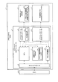
具体的には、メモリシステム1は、図1に示すように構成され得る。図1は、メモリシステム1の構成を示す図である。
Specifically, the
メモリシステム1は、通信バスを介してホストHAの外部に接続され、ホストHAに対する外部記憶装置として機能する。ホストHAは、例えば、パーソナルコンピュータ又はCPUコアを含む。メモリシステム1は、例えば、SSD(Solid State Drive)を含む。
The
メモリシステム1は、コントローラ2、揮発性メモリ3、及び不揮発性メモリ4を有する。メモリシステム1がSSDである場合、コントローラ2は、SSDコントローラとすることができる。コントローラ2は、例えばSoC(System−on−a−Chip)を含むコントローラパッケージとして実装され得る。コントローラ2は、データ等を一時記憶するためのキャッシュメモリとして揮発性メモリ7を含む。
The
揮発性メモリ3は、コントローラ2外に配され、揮発性メモリパッケージとして実装され得る。揮発性メモリ3は、コントローラ2内の揮発性メモリ7よりアクセススピードが遅いがビット当たりの単価が安い揮発性メモリであり、揮発性メモリ7より記憶容量が大きく構成され得る。揮発性メモリ3は、例えば、DRAM(Dynamic Random Access Memory)とすることができる。
The
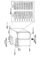
不揮発性メモリ4は、コントローラ2外に配され、不揮発性メモリパッケージとして実装され得る。不揮発性メモリ4は、例えばNAND型フラッシュメモリとすることができるがこれに限定されない。不揮発性メモリ4は、例えばReRAM(Resistance Random Access Memory)、PRAM(Phase change RAM)、MRAM(Magnetoresistive Random Access Memory)、又は、FeRAM(Ferroelectric Random Access Memory)であってもよい。不揮発性メモリ4は、複数の物理ブロックを有する。各物理ブロックは、データ消去の単位である。各物理ブロックは、複数のメモリセルを有する。各メモリセルは多値記憶が可能である。各物理ブロックにおける同一のワード線に接続されたメモリセル群は、各メモリセルがシングルレベルセルである場合に1つの物理ページとして扱われ、各メモリセルがマルチレベルセルである場合に2つの物理ページとして扱われ、各メモリセルがトリプルレベルセルである場合に3つの物理ページとして扱われる。不揮発性メモリ4におけるデータ管理単位は、図2に示すように構成され得る。図2は、不揮発性メモリ4のデータの管理単位を示す図である。
The
不揮発性メモリ4は、複数のメモリチップで構成され得る。各メモリチップ内部において、一括してデータの書き込みおよび読み出しのアクセスが可能な単位が物理ページである。複数の物理ページから構成され、独立してデータの消去が可能な最小のアクセス単位が物理ブロックである。また、図2に示す例では、8つのチャネルch0〜ch7にメモリチップが接続されている場合が例示されている。コントローラ2は、各チャネルch0〜ch7を互いに並列して制御することが可能である。また、コントローラ2は、各チャネルch0〜ch7についてさらにバンクインタリーブにより複数の並列動作を行うことが可能である。これにより、並列にほぼ一括して書き込み/読み出しが可能な16個の物理ページでデータ記録領域となる1論理ページを構成でき、並列にほぼ一括して消去可能な16個の物理ブロックでデータブロックである1論理ブロックを構成することができる。ガーベージコレクションは、この1論理ブロックの単位で行われ得る。
The
また、1物理ページよりも小さい単位のデータ管理単位であるクラスタで、CPU6により、不揮発性メモリ4内でのデータが管理されるものとする。クラスタサイズは、ホストHAからの最小アクセス単位であるセクタのサイズ以上であり、クラスタサイズの自然数倍が物理ページサイズとなるように定められる。例えば、1物理ページは4クラスタで構成され、1論理ページは64クラスタで構成され得る。なお、各チャネルで並列に一括してデータ書き込みを行うため、この実施形態では、データはクラスタ番号順に格納されることになる。
It is also assumed that the
図1に戻って、コントローラ2は、メモリシステム1における各部を統括的に制御する。コントローラ2は、揮発性メモリ7に加えて、ホストコントローラ5、プロセッサ(CPU:Central Processing Unit)6、ブロック管理部8、メモリコントローラ9、及びメモリコントローラ10を有する。
Returning to FIG. 1, the
CPU6は、ファームウェアを実行することにより、コントローラ2における各部を統括的に制御する。
The
ホストコントローラ5は、CPU6による制御のもと、ホストHAに対するインターフェース動作を行う。ホストコントローラ5は、ホストHAから受信したコマンド及び/又はデータをCPU6及び/又はブロック管理部8へ供給する。例えば、ホストコントローラ5は、ホストライト要求及びライトデータをホストHAから受信すると、ホストライト要求及びライトデータをCPU6へ転送するとともにホストライト要求をブロック管理部8へ転送する。また、ホストコントローラ5は、CPU6から供給された通知及び/又はデータをホストHAへ送信する。
The
メモリコントローラ9は、CPU6による制御のもと、揮発性メモリ3に対するインターフェース動作を行う。揮発性メモリ3がDRAMである場合、メモリコントローラ9は、DRAMコントローラとすることができる。また、メモリコントローラ9は、加減算回路11を有する。加減算回路11は、有効クラスタ数を更新するために用いられる。
The
メモリコントローラ10は、CPU6による制御のもと、不揮発性メモリ4に対するインターフェース動作を行う。不揮発性メモリ4がNAND型フラッシュメモリである場合、メモリコントローラ9は、NANDコントローラとすることができる。
The
揮発性メモリ7は、コントローラ2内に配され、コントローラ2内(コントローラパッケージ内)の回路として実装され得る。揮発性メモリ7は、揮発性メモリ3よりアクセススピードが速いがビット当たりの単価が高い揮発性メモリであり、揮発性メモリ3より記憶容量が小さく構成され得る。揮発性メモリ7は、例えば、SRAM(Static Random Access Memory)とすることができる。
The
揮発性メモリ7は、アドレス変換情報7aを格納する。アドレス変換情報7aは、不揮発性メモリ4へアクセスするための論理アドレス及び物理アドレス間の変換に用いられる情報であり、ルックアップテーブル(LUT:Look Up Table)とも呼ばれ得る。アドレス変換情報7aは、ホストHAからの不揮発性メモリ4へのアクセス(例えば、ホストライト、ホストリード)が行われる度に更新され得る。
The
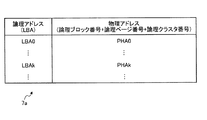
アドレス変換情報7aは、例えば、図3に示すようなデータ構造を有する。図3は、アドレス変換情報7aのデータ構造を示す図である。図3では、アドレス変換情報7aがテーブル形式で(論物変換テーブルとして)構成される場合が例示されている。アドレス変換情報7aでは、論理アドレスと物理アドレスとが対応付けされている。論理アドレスは、例えば、LBA(Logical Block Address)とすることができる。物理アドレスは、論理ブロックの識別情報(例えば、論理ブロック番号)と論理クラスタの識別情報(例えば、論理ページ番号+論理クラスタ番号)との組み合わせとすることができる。例えば、図3に示すアドレス変換情報7aを参照することで、論理アドレスLBA0と物理アドレスPHA0とが対応していることが分かり、論理アドレスLBAkと物理アドレスPHAkとが対応していることが分かる。
The
図1に示すブロック管理部8は、不揮発性メモリ4における各ブロックの管理を行う。例えば、メモリシステム1が起動されると、CPU6は、メモリコントローラ10及びメモリコントローラ9を制御して、不揮発性メモリ4における管理情報格納領域に格納されたブロック管理情報12を読み出して揮発性メモリ3に格納する。
The
ブロック管理情報12は、ブロックの識別情報と有効クラスタ数とが複数のブロックについて対応付けられた管理情報であり、有効クラスタカウンタとも呼ばれ得る。例えば、ブロック管理情報12は、図4に示すようなデータ構造を有する。図4は、ブロック管理情報12(有効クラスタカウンタ)のデータ構造を示す図である。図4では、ブロック管理情報12がテーブル形式で(すなわち、有効クラスタカウンタテーブルとして)構成される場合が例示されている。ブロック管理情報12では、論理ブロックの識別情報(例えば、論理ブロック番号)と有効クラスタ数とが対応付けされている。例えば、図4に示すブロック管理情報12を参照することで、論理ブロックBL0の有効クラスタ数が「CC0」であることが分かり、論理ブロックBLnの有効クラスタ数が「CCn」であることが分かる。
The
このブロック管理情報12は、図5及び図6に示すように更新され得る。図5は、メモリシステム1の動作を示すシーケンス図である。図6は、メモリシステム1の動作例を示す図である。
This
ブロック管理部8は、ホストライト要求を受けると(S1)、ホストライト要求に応じて、不揮発性メモリ4におけるライトが行われるブロックを特定する。ブロック管理部8は、揮発性メモリ7に格納されたアドレス変換情報7aを参照することなどにより、ホストライト要求に対応する論理ブロックを特定する(S2)。ブロック管理部8は、特定された論理ブロックに対する有効クラスタ数の更新指示を生成してメモリコントローラ9へ供給する(S3)。有効クラスタ数の更新指示は、ブロックの識別情報に対応付けられた更新量を含む。ブロックの識別情報は、有効クラスタ数を更新すべき論理ブロックの識別情報(例えば、論理ブロック番号)を含む。更新量は、有効クラスタ数を更新すべき量(例えば、インクリメント(+1)、又はディクリメント(−1))を含む。
Upon receiving the host write request (S1), the
これにより、メモリコントローラ9は、揮発性メモリ3にアクセスし(S4)、揮発性メモリ3から更新指示に応じた有効クラスタ数を読み出す(S5)。メモリコントローラ9は、加減算回路11を用いて、読み出された有効クラスタ数を更新指示に応じた更新量で更新する(S6)。更新指示に応じた更新量が「+1」である場合、加減算回路11は、有効クラスタ数をインクリメント(+1)する。更新指示に応じた更新量が「−1」である場合、加減算回路11は、有効クラスタ数をディクリメント(−1)する。メモリコントローラ9は、更新された有効クラスタ数を揮発性メモリ3へ書き戻す(S7)。これにより、揮発性メモリ3に格納されたブロック管理情報12が更新され得る。なお、コントローラ2は、メモリコントローラ10によるホストライトの実行が完了している場合、ホストライト要求に対応するライト完了通知を、S6の完了後にホストコントローラ5からホストHAへ行ってもよいし、S6を待たずにS3の完了後にホストコントローラ5からホストHAへ行ってもよい。
As a result, the
例えば、図6には、不揮発性メモリ4が4つの論理ブロックBL0〜BL3を有し、各論理ブロックBL0〜BL3が5つの論理クラスタCL0〜CL4を有する場合の動作例が例示されている。なお、以下の説明において、CPU6が実行すると説明されている機能は所定の専用回路で実行されてもよいし、所定の専用回路で実行されると説明されている機能は、CPU6で実行されてもよい。また、図6の右図において、×が記載された四角は無効クラスタを表し、空白の四角は消去済みで未書き込みのクラスタを表す。
For example, FIG. 6 illustrates an operation example in a case where the
タイミングt1の直前において、論理ブロックBL0における論理クラスタCL2〜CL4、論理ブロックBL1における論理クラスタCL1,CL2,CL4、論理ブロックBL2における論理クラスタCL1,CL4がそれぞれ無効クラスタであり、論理ブロックBL3がフリーブロックとなっている。 Immediately before the timing t1, the logical clusters CL2 to CL4 in the logical block BL0, the logical clusters CL1, CL2, and CL4 in the logical block BL1, the logical clusters CL1 and CL4 in the logical block BL2 are invalid clusters, and the logical block BL3 is a free block. It has become.
ブロック管理情報12では、論理ブロックBL0,BL1,BL2,BL3の有効クラスタ数がそれぞれ、「0」、「0」、「0」、「0」となっている。
In the
タイミングt1において、論理アドレスAを含むホストライト要求とデータBを含むライトデータとがホストコントローラ5で受信される。
At timing t1, a host write request including the logical address A and write data including the data B are received by the
タイミングt2において、ホストライト要求とライトデータとが転送されると、CPU6は、「アドレスA」の論理アドレスに対して「BL0,CL0」の物理アドレスを割り当て、アドレス変換情報7aをそのように更新する。CPU6は、ホストライト要求とライトデータとをメモリコントローラ10へ転送する。メモリコントローラ10は、不揮発性メモリ4にアクセスし、論理ブロックBL0の論理クラスタCL0に対応する位置にデータBを書き込む。
When the host write request and the write data are transferred at the timing t2, the
また、ホストライト要求が転送されると、ブロック管理部8は、ホストライト要求に含まれた論理アドレス「アドレスA」に対応する論理ブロックの識別情報「BL0」を特定する。ブロック管理部8は、特定結果に応じて、論理ブロックBL0の有効クラスタ数をインクリメント(+1)すべきであると判断し、論理ブロックの識別情報「BL0」に対応付けられた更新量「+1」を含む更新指示を作成してメモリコントローラ9へ供給する。
When the host write request is transferred, the
タイミングt3において、更新指示を受けると、メモリコントローラ9は、揮発性メモリ3から更新指示に応じた論理ブロックBL0の有効クラスタ数「0」を読み出す。メモリコントローラ9は、読み出された有効クラスタ数「0」を更新指示に応じた更新量「+1」で更新する。メモリコントローラ9は、更新された有効クラスタ数「1」を揮発性メモリ3へ書き戻す。これにより、揮発性メモリ3に格納されたブロック管理情報12において、論理ブロックBL0の有効クラスタ数が「0」→「1」に更新される。
At time t3, when receiving the update instruction, the
タイミングt4において、論理アドレスCを含むホストライト要求とデータDを含むライトデータとがホストコントローラ5で受信される。
At timing t4, the
タイミングt5において、ホストライト要求とライトデータとが転送されると、CPU6は、「アドレスC」の論理アドレスに対して「BL0,CL1」の物理アドレスを割り当て、アドレス変換情報7aをそのように更新する。CPU6は、ホストライト要求とライトデータとをメモリコントローラ10へ転送する。メモリコントローラ10は、不揮発性メモリ4にアクセスし、論理ブロックBL0の論理クラスタCL1に対応する位置にデータDを書き込む。
At timing t5, when the host write request and the write data are transferred, the
また、ホストライト要求が転送されると、ブロック管理部8は、ホストライト要求に含まれた論理アドレス「論理アドレスC」に対応する論理ブロックの識別情報「BL0」を特定する。ブロック管理部8は、特定結果に応じて、論理ブロックBL0の有効クラスタ数をインクリメント(+1)すべきであると判断し、論理ブロックの識別情報「BL0」に対応付けられた更新量「+1」を含む更新指示を作成してメモリコントローラ9へ供給する。
When the host write request is transferred, the
タイミングt6において、更新指示を受けると、メモリコントローラ9は、揮発性メモリ3から更新指示に応じた論理ブロックBL0の有効クラスタ数「1」を読み出す。メモリコントローラ9は、読み出された有効クラスタ数「1」を更新指示に応じた更新量「+1」で更新する。メモリコントローラ9は、更新された有効クラスタ数「2」を揮発性メモリ3へ書き戻す。これにより、揮発性メモリ3に格納されたブロック管理情報12において、論理ブロックBL0の有効クラスタ数が「1」→「2」に更新される。
Upon receiving the update instruction at timing t6, the
タイミングt7において、論理アドレスAを含むホストライト要求とデータEを含むライトデータとがホストコントローラ5で受信される。
At timing t7, the
タイミングt8において、ホストライト要求とライトデータとが転送されると、CPU6は、「アドレスA」の論理アドレスに対して「BL0,CL0」に代えて「BL1,CL0」の物理アドレスを割り当て、アドレス変換情報7aをそのように更新する。すなわち、アドレス変換情報7aにおける「アドレスA」の論理アドレスに対応する古い対応情報を削除し、「アドレスA」の論理アドレスが「BL1,CL0」の物理アドレスに対応付けられた新しい対応情報を追加する。論理ブロックBL0の論理クラスタCL0は、アドレス変換情報7a中に対応する論理アドレスが存在しなくなり、無効化される。CPU6は、ホストライト要求とライトデータとをメモリコントローラ10へ転送する。メモリコントローラ10は、論理ブロックBL1の論理クラスタCL0にデータEを書き込む。
At timing t8, when the host write request and the write data are transferred, the
また、ホストライト要求が転送されると、ブロック管理部8は、ホストライト要求に含まれた論理アドレス「アドレスA」に対応する旧論理ブロックの識別情報「BL0」と新論理ブロックの識別情報「BL1」とを特定する。ブロック管理部8は、特定結果に応じて、論理ブロックBL0の有効クラスタ数をディクリメント(−1)し論理ブロックBL1の有効クラスタ数をインクリメント(+1)すべきであると判断し、論理ブロックの識別情報「BL0」に対応付けられた更新量「−1」と論理ブロックの識別情報「BL1」に対応付けられた更新量「+1」とを含む更新指示を作成してメモリコントローラ9へ供給する。
Further, when the host write request is transferred, the
タイミングt9において、更新指示を受けると、メモリコントローラ9は、揮発性メモリ3から更新指示に応じた論理ブロックBL0の有効クラスタ数「2」と論理ブロックBL1の有効クラスタ数「0」とを読み出す。メモリコントローラ9は、読み出された論理ブロックBL0の有効クラスタ数「2」を更新指示に応じた更新量「−1」で更新し、読み出された論理ブロックBL1の有効クラスタ数「0」を更新指示に応じた更新量「+1」で更新する。メモリコントローラ9は、論理ブロックBL0について更新された有効クラスタ数「1」と論理ブロックBL1について更新された有効クラスタ数「1」とを揮発性メモリ3へ書き戻す。これにより、揮発性メモリ3に格納されたブロック管理情報12において、論理ブロックBL0の有効クラスタ数が「2」→「1」に更新され、論理ブロックBL1の有効クラスタ数が「0」→「1」に更新される。
At timing t9, when receiving the update instruction, the
同様に、図示しないが、論理アドレス「F」、「H」、「J」、「L」と物理アドレス「BL1,CL3」、「BL2,CL0」、「BL2,CL2」、「BL2,CL3」との対応情報がアドレス変換情報7aに記録される。それとともに、不揮発性メモリ4における物理アドレス「BL1,CL3」、「BL2,CL0」、「BL2,CL2」、「BL2,CL3」に、それぞれ、データ「G」、「I」、「K」、「M」が書き込まれる。
Similarly, although not shown, the logical addresses “F”, “H”, “J”, “L” and the physical addresses “BL1, CL3”, “BL2, CL0”, “BL2, CL2”, “BL2, CL3” Is recorded in the
これに応じて、タイミングt10において、ブロック管理情報12では、論理ブロックBL0,BL1,BL2,BL3の有効クラスタ数がそれぞれ、「1」、「2」、「3」、「0」と更新されている。なお、図6では、図示の簡略化のため、アドレス変換情報7aにおける論理アドレス「F」、「H」、「J」、「L」と物理アドレス「BL1,CL3」、「BL2,CL0」、「BL2,CL2」、「BL2,CL3」との対応情報の図示が省略されている。
In response to this, at the timing t10, in the
図5に示すブロック管理部8は、ガーベージコレクション要求をCPU6から受けると(S8)、ブロック管理情報12の取得指示をメモリコントローラ9へ転送する(S9)。
When receiving the garbage collection request from the CPU 6 (S8), the
これにより、メモリコントローラ9は、揮発性メモリ3にアクセスし(S10)、揮発性メモリ3から取得指示に応じたブロック管理情報12を読み出す(S11)。メモリコントローラ9は、読み出されたブロック管理情報12をブロック管理部8へ転送する(S12)。
As a result, the
ブロック管理部8は、ブロック管理情報12を用いて、不揮発性メモリ4における複数のブロックのうちガーベージコレクションの対象となるブロックを決定する(S13)。ブロック管理部8は、ブロック管理情報12を参照し、複数のブロックのうち有効クラスタ数が閾値以下のブロックをソースブロックとして選択してもよいし、複数のブロックのうちフリーブロックを除き有効クラスタ数が少ない順にブロックを選択しソースブロックとしてもよい。ブロック管理部8は、ブロック管理情報12を参照し、フリーブロックを特定してデスティネーションブロックとしてもよい。ブロック管理部8は、ソースブロックとデスティネーションブロックとを指定してガーベージコレクションを行わせる実行指示を生成してメモリコントローラ10へ転送する(S14)。
The
これにより、メモリコントローラ10は、不揮発性メモリ4にアクセスし(S15)、ガーベージコレクションを行うように不揮発性メモリ4に指示する。不揮発性メモリ4は、その指示に応じて、ガーベージコレクションを行う(S16)。すなわち、不揮発性メモリ4は、ソースブロックから有効クラスタのデータを集めてデスティネーションブロックに書き直すデータの引っ越し処理を行い、データの引っ越し処理が完了すると、ソースブロックに対してデータの消去処理を行い、ソースブロックをフリーブロックとする。
As a result, the
例えば、図6に示すタイミングt11において、ガーベージコレクション要求をCPU6から受けると、ブロック管理部8は、タイミングt10に更新されたブロック管理情報12を参照し、複数のブロックBL0〜BL3のうち有効クラスタ数が閾値(例えば、2)以下のブロックBL0,BL1をソースブロックとして選択する。あるいは、ブロック管理部8は、ブロック管理情報12を参照し、複数のブロックBL0〜BL3のうちフリーブロックを除き有効クラスタ数が少ない順に所定数のブロック(例えば、2つのブロック)BL0,BL1を選択しソースブロックとする。ブロック管理部8は、ブロック管理情報12を参照し、有効クラスタ数がゼロであるブロックBL3をフリーブロックとして特定してデスティネーションブロックとする。ブロック管理部8は、ソースブロックBL0,BL1とデスティネーションブロックBL3とを指定してガーベージコレクションを行わせる実行指示を生成してメモリコントローラ10へ転送する。
For example, when a garbage collection request is received from the
タイミングt12において、実行指示を受けると、メモリコントローラ10は、不揮発性メモリ4にアクセスし、ガーベージコレクションを行うように指示するコマンドを発行して不揮発性メモリ4へ供給する。不揮発性メモリ4は、そのコマンドに応じて、ガーベージコレクションを行う。すなわち、不揮発性メモリ4は、ソースブロックBL0から有効クラスタCL1のデータを集め、ソースブロックBL1から有効クラスタCL0,CL3のデータを集めてデスティネーションブロックBL3に書き直すデータの引っ越し処理を行う。不揮発性メモリ4は、データの引っ越し処理が完了すると、ソースブロックBL0,BL1に対してデータの消去処理を行う。これにより、ソースブロックBL0,BL1をフリーブロックとすることができ、不揮発性メモリ4におけるストレージ領域を効率的に確保することができる。
At timing t12, when receiving the execution instruction, the
図5に示す不揮発性メモリ4は、ガーベージコレクションが完了すると、完了通知をメモリコントローラ10へ返す(S17)。これに応じて、メモリコントローラ10は、完了通知をブロック管理部8へ転送する(S18)。ブロック管理部8は、完了通知をCPU6へ転送する(S19)。これにより、CPU6は、ガーベージコレクションが完了したことを認識するとともにアドレス変換情報7aを更新する。また、ブロック管理部8は、完了通知に応じて、データの引っ越し処理が行われた論理ブロックと消去処理が行われた論理ブロックとをそれぞれ特定する(S20)。ブロック管理部8は、特定された論理ブロックに対する有効クラスタ数の更新指示を生成してメモリコントローラ9へ供給する(S21)。有効クラスタ数の更新指示は、ブロックの識別情報に対応付けられた更新量を含む。ブロックの識別情報は、有効クラスタ数を更新すべき論理ブロックの識別情報(例えば、論理ブロック番号)を含む。更新量は、有効クラスタ数を更新すべき量(例えば、インクリメント(+1)、又はディクリメント(−1))を含む。
When the garbage collection is completed, the
これにより、メモリコントローラ9は、揮発性メモリ3にアクセスし(S22)、揮発性メモリ3から更新指示に応じた有効クラスタ数を読み出す(S23)。メモリコントローラ9は、加減算回路11を用いて、読み出された有効クラスタ数を更新指示に応じた更新量で更新する(S24)。更新指示に応じた更新量が「+1」である場合、加減算回路11は、有効クラスタ数をインクリメント(+1)する。更新指示に応じた更新量が「−1」である場合、加減算回路11は、有効クラスタ数をディクリメント(−1)する。メモリコントローラ9は、更新された有効クラスタ数を揮発性メモリ3へ書き戻す(S25)。これにより、揮発性メモリ3に格納されたブロック管理情報12が更新され得る。
As a result, the
例えば、図6に示すタイミングt13において、完了通知が転送されると、CPU6は、データDの記憶位置が変更されたことに応じて、「アドレスC」の論理アドレスに対して「BL0,CL1」に代えて「BL3,CL1」の物理アドレスを割り当て、アドレス変換情報7aをそのように更新する。CPU6は、データEの記憶位置が変更されたことに応じて、「アドレスA」の論理アドレスに対して「BL1,CL0」に代えて「BL3,CL0」の物理アドレスを割り当て、アドレス変換情報7aをそのように更新する。CPU6は、データGの記憶位置の変更についても、図示しないが、アドレス変換情報7aを更新する。
For example, when the completion notification is transferred at the timing t13 shown in FIG. 6, the
また、完了通知が転送されると、ブロック管理部8は、完了通知に応じて、データの引っ越し処理が行われた論理ブロックBL0,BL1,BL3と消去処理が行われた論理ブロックBL0,BL1とをそれぞれ特定する。ブロック管理部8は、特定結果に応じて、論理ブロックBL0の有効クラスタ数を−1して0にし論理ブロックBL1の有効クラスタ数を−2して0にし論理ブロックBL1の有効クラスタ数を+3して3にすべきであると判断し、論理ブロックの識別情報「BL0」に対応付けられた更新量「−1」と論理ブロックの識別情報「BL1」に対応付けられた更新量「−2」と論理ブロックの識別情報「BL3」に対応付けられた更新量「+3」とを含む更新指示を作成してメモリコントローラ9へ供給する。
When the completion notification is transferred, the
タイミングt14において、更新指示を受けると、メモリコントローラ9は、揮発性メモリ3から更新指示に応じた論理ブロックBL0の有効クラスタ数「1」と論理ブロックBL1の有効クラスタ数「2」と論理ブロックBL3の有効クラスタ数「0」とを読み出す。メモリコントローラ9は、読み出された論理ブロックBL0の有効クラスタ数「1」を更新指示に応じた更新量「−1」で更新し、読み出された論理ブロックBL1の有効クラスタ数「2」を更新指示に応じた更新量「−2」で更新し、読み出された論理ブロックBL3の有効クラスタ数「0」を更新指示に応じた更新量「+3」で更新する。メモリコントローラ9は、論理ブロックBL0について更新された有効クラスタ数「0」と論理ブロックBL1について更新された有効クラスタ数「0」と論理ブロックBL3について更新された有効クラスタ数「3」とを揮発性メモリ3へ書き戻す。これにより、揮発性メモリ3に格納されたブロック管理情報12において、論理ブロックBL0の有効クラスタ数が「1」→「0」に更新され、論理ブロックBL1の有効クラスタ数が「2」→「0」に更新され、論理ブロックBL3の有効クラスタ数が「0」→「3」に更新される。
At timing t14, when receiving the update instruction, the
以上のように、実施形態では、メモリシステム1において、コントローラ2における有効クラスタ数の更新動作をブロック管理部8に代えてコントローラ外の揮発性メモリ3に対するI/Fとなるメモリコントローラ9で行えるようにする。これにより、不揮発性メモリ4が大容量化しブロック管理情報(有効クラスタカウンタ)12のデータ容量が増大した場合に、コントローラ2内の揮発性メモリ7を大容量化することなく(すなわち、メモリシステム1のコスト増加を抑制しながら)、有効クラスタ数の更新処理に要する時間を容易に短縮化できる。
As described above, in the embodiment, in the
例えば、図7に示すように、少なくとも、揮発性メモリ3から読み出された有効クラスタ数をメモリコントローラ9からブロック管理部8へ転送する際の転送遅延TP01と更新された有効クラスタ数をブロック管理部8からメモリコントローラ9へ転送する際の転送遅延TP02とを削減できる。この結果、ブロック管理部8で更新動作を行う場合の処理時間TP0に比較して、実施形態では、有効クラスタ数の更新処理をΔTP1短縮された処理時間TP1で実現できる。
For example, as shown in FIG. 7, at least the transfer delay TP01 when transferring the number of valid clusters read from the
なお、有効クラスタ数の複数回の更新動作を一括して行うことができれば、メモリコントローラ9による揮発性メモリ3への平均的なアクセス頻度を低減でき、有効クラスタ数の更新処理の平均的な処理時間をさらに低減できると期待できる。
If the update operation of the number of valid clusters can be performed collectively, the average frequency of access to the
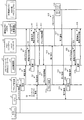
そのような考えに基づき、図8に示すように、メモリコントローラ9内にキャッシュ領域213を設けてもよい。図8は、実施形態の第1変形例に係るメモリシステム1の構成の一部及び動作を示すデータフロー図である。キャッシュ領域213は、例えばSRAMで実現され得る。
Based on such a concept, a cache area 213 may be provided in the
例えば、有効クラスタ数の3回の更新動作を一括して行う場合について説明する。ブロック管理部8は、1回目のホストライト要求(S1−1)に対応する論理ブロックを特定し(S2−1)、1回目の有効クラスタ数の更新指示を生成してメモリコントローラ9へ供給する(S3−1)。メモリコントローラ9は、更新指示に応じた更新量をブロックごとに識別情報に対応付けて集計し、識別情報に対応付けられた積算更新量をキャッシュ領域213に格納する(S201−1)。
For example, a case where three updating operations of the number of valid clusters are collectively performed will be described. The
ブロック管理部8は、2回目のホストライト要求(S1−2)に対応する論理ブロックを特定し(S2−2)、2回目の有効クラスタ数の更新指示を生成してメモリコントローラ9へ供給する(S3−2)。メモリコントローラ9は、更新指示に応じた更新量をブロックごとに識別情報に対応付けて集計し、識別情報に対応付けられた積算更新量をキャッシュ領域213に格納する(S201−2)。
The
ブロック管理部8は、3回目のホストライト要求(S1−3)に対応する論理ブロックを特定し(S2−3)、3回目の有効クラスタ数の更新指示を生成してメモリコントローラ9へ供給する(S3−3)。メモリコントローラ9は、更新指示に応じた更新量をブロックごとに識別情報に対応付けて集計し、識別情報に対応付けられた積算更新量をキャッシュ領域213に格納する(S201−3)。
The
そして、メモリコントローラ9は、揮発性メモリ3にアクセスし(S4)、揮発性メモリ3から更新指示に応じた有効クラスタ数を読み出す(S5)。メモリコントローラ9は、加減算回路11を用いて、読み出された有効クラスタ数を積算更新量で更新する(S6)。メモリコントローラ9は、更新された有効クラスタ数を揮発性メモリ3へ書き戻す(S7)。これにより、揮発性メモリ3に格納されたブロック管理情報12が更新され得る。
Then, the
例えば、図6に示す動作例では、タイミングt1のホストライト要求に応じて、タイミングt2において、論理ブロックの識別情報「BL0」に対応付けられた更新量「+1」を含む更新指示がメモリコントローラ9へ供給される。
For example, in the operation example shown in FIG. 6, in response to the host write request at timing t1, at timing t2, the
タイミングt3において、更新指示を受けると、メモリコントローラ9は、論理ブロックの識別情報「BL0」に対応付けられた積算更新量「+1」を生成してキャッシュ領域213に格納する。
At timing t3, when receiving the update instruction, the
タイミングt4のホストライト要求に応じて、タイミングt5において、論理ブロックの識別情報「BL0」に対応付けられた更新量「+1」を含む更新指示がメモリコントローラ9へ供給される。
In response to the host write request at timing t4, an update instruction including the update amount “+1” associated with the logical block identification information “BL0” is supplied to the
タイミングt6において、更新指示を受けると、メモリコントローラ9は、キャッシュ領域213から積算更新量を読み出し、論理ブロックの識別情報「BL0」に対応付けられた積算更新量「+1」に更新量「+1」を加算し、積算更新量「+2」を求める。メモリコントローラ9は、論理ブロックの識別情報「BL0」に対応付けられた積算更新量「+2」をキャッシュ領域213に格納する。
At time t6, when receiving the update instruction, the
タイミングt7のホストライト要求に応じて、タイミングt8において、論理ブロックの識別情報「BL0」に対応付けられた更新量「−1」と論理ブロックの識別情報「BL1」に対応付けられた更新量「+1」とを含む更新指示がメモリコントローラ9へ供給される。
In response to the host write request at timing t7, at timing t8, the update amount “−1” associated with the logical block identification information “BL0” and the update amount “1” associated with the logical block identification information “BL1” An update instruction including “+1” is supplied to the
タイミングt9において、更新指示を受けると、メモリコントローラ9は、キャッシュ領域213から積算更新量を読み出し、論理ブロックの識別情報「BL0」に対応付けられた積算更新量「+2」に更新量「−1」を加算し、積算更新量「+1」を求める。メモリコントローラ9は、論理ブロックの識別情報「BL0」に対応付けられた積算更新量「+1」をキャッシュ領域213に格納する。また、メモリコントローラ9は、論理ブロックの識別情報「BL1」に対応付けられた積算更新量「0」に更新量「+1」を加算し、積算更新量「+1」を求める。メモリコントローラ9は、論理ブロックの識別情報「BL1」に対応付けられた積算更新量「+1」をキャッシュ領域213に格納する。
At time t9, when receiving the update instruction, the
そして、メモリコントローラ9は、揮発性メモリ3から論理ブロックBL0の有効クラスタ数「0」と論理ブロックBL1の有効クラスタ数「0」とを読み出す。メモリコントローラ9は、読み出された論理ブロックBL0の有効クラスタ数「0」を1回目〜3回目の更新指示に応じた積算更新量「+1」で更新し、読み出された論理ブロックBL1の有効クラスタ数「1」を1回目〜3回目の更新指示に応じた積算更新量「+1」で更新する。メモリコントローラ9は、論理ブロックBL0について更新された有効クラスタ数「1」と論理ブロックBL1について更新された有効クラスタ数「2」とを揮発性メモリ3へ書き戻す。これにより、揮発性メモリ3に格納されたブロック管理情報12において、論理ブロックBL0の有効クラスタ数が「0」→「1」に更新され、論理ブロックBL1の有効クラスタ数が「0」→「1」に更新される。
Then, the
このように、有効クラスタ数の複数回の更新動作を一括して行うことができれば、メモリコントローラ9による揮発性メモリ3への平均的なアクセス頻度を低減でき、有効クラスタ数の更新処理の平均的な処理時間をさらに低減できる。
As described above, if the updating operation of the number of valid clusters can be performed collectively, the average frequency of access to the
例えば、図9に示すように、少なくとも、複数回のうち最終回を除く各回の更新処理時間TP1−1,TP1−2における更新後の有効クラスタ数を揮発性メモリ3へ書き込む時間TP111−1,TP111−2を削減できる。この結果、毎回更新動作を行う場合の処理時間TP11に比較して、実施形態の第1変形例では、有効クラスタ数の更新処理をΔTP12短縮された処理時間TP12で実現できる。
For example, as shown in FIG. 9, at least a time TP111-1 for writing the number of valid clusters after updating in the update processing times TP1-1 and TP1-2 in the
なお、有効クラスタ数の複数回の更新動作を一括して行うトリガー条件は、更新動作の回数が所定回数に達したことであってもよいし、積算更新量のデータ容量がキャッシュ領域213の記憶容量に達したことであってもよいし、ガーベージコレクション時であってもよい。 Note that the trigger condition for performing a plurality of update operations of the number of valid clusters collectively may be that the number of update operations reaches a predetermined number, or the data capacity of the integrated update amount is stored in the cache area 213. It may be that the capacity has been reached, or it may be at the time of garbage collection.
例えば有効クラスタ数の複数回の更新動作をガーベージコレクション時に行う場合、次の動作が行われてもよい。ガーベージコレクション時には、CPU6がブロック管理部8、メモリコントローラ9を通じて揮発性メモリ3にアクセスして有効カウンタ数を読み込んでおく。このときに、メモリコントローラ9は、キャッシュ領域213の中に読み込み先の論理ブロックに関するエントリがあるか確認し、必要に応じて加減算処理を行う。あるいは、キャッシュ領域213内で、ガーベージコレクションの結果に応じた積算値を保持し、これをアイドル時等の空き時間に揮発性メモリ3に書き戻してもよい。この構成により、揮発性メモリ(DRAM)3に対するアクセス頻度を少なくすることができる。
For example, when performing the updating operation of the number of valid clusters a plurality of times at the time of garbage collection, the following operation may be performed. At the time of garbage collection, the
あるいは、揮発性メモリ3が複数のリフレッシュ領域を有する場合、有効クラスタ数の更新のためのメモリアクセスを複数のリフレッシュ領域のうちリフレッシュされていないリフレッシュ領域に対して行えば、有効クラスタ数の更新処理を揮発性メモリ3のリフレッシュ処理との関係で効率化できると期待できる。
Alternatively, in the case where the
そのような考えに基づき、図10に示すように、揮発性メモリ3が複数のリフレッシュ領域14−1〜14−k(kは2以上の整数)を有することに対応して、メモリコントローラ9内にキャッシュ領域313−1〜313−kを設けてもよい。各リフレッシュ領域14は、揮発性メモリ3におけるリフレッシュ処理、すなわち定期的なメモリセルへの電荷の充電の処理を行う単位となる領域であり、例えば、DIMM領域(すなわち、電源の供給単位となる領域)であってもよいし、ランク領域(すなわち、1メモリチップとなる領域)であってもよいし、バンク領域(メモリコントローラ9が揮発性メモリ3を管理する単位となる領域)であってもよい。
Based on such an idea, as shown in FIG. 10, in response to the
例えば、CPU6は、不揮発性メモリ4におけるストレージ領域のアドレス空間を論理ブロックの単位でリフレッシュ領域の数(k個)に分割して、k個のリフレッシュ領域14−1〜14−kとk個のキャッシュ領域313−1〜313−kとにそれぞれ割り当てる。
For example, the
メモリシステム1が起動されると、CPU6は、メモリコントローラ10及びメモリコントローラ9を制御して、不揮発性メモリ4における管理情報格納領域に格納されたブロック管理情報12を読み出して揮発性メモリ3に格納する。このとき、CPU6は、ブロック管理情報12における各論理ブロックのレコード(論理ブロック番号と有効クラスタ数との対応情報)がその論理ブロックに割り当てられたリフレッシュ領域14に格納されるように制御する。図10では、ブロック管理情報12は、k個のリフレッシュ領域14−1〜14−kに跨って揮発性メモリ3内に格納される場合が例示されている。
When the
メモリコントローラ9は、CPU6による制御のもと、不揮発性メモリ4における複数の論理ブロックとk個のキャッシュ領域313−1〜313−kとの対応関係に応じて、各論理ブロックの有効クラスタ数に対する積算更新量をその論理ブロックに対応するキャッシュ領域313に格納する。メモリコントローラ9は、一括更新のタイミングになると、そのキャッシュ領域313に対応するリフレッシュ領域14から有効クラスタ数を読み出し、そのキャッシュ領域313に格納された積算更新量で更新し、更新された有効クラスタ数をそのリフレッシュ領域14へ書き戻す。この更新された有効クラスタ数をそのリフレッシュ領域14へ書き戻す処理を、CPU6は、他のリフレッシュ領域14に対するリフレッシュ処理と並行して行うように制御することができる。
The
例えば、k=2である場合、図11に示すように、有効クラスタ数の更新処理と揮発性メモリ3に対するリフレッシュ処理とを並行させることができる。図11は、実施形態の第2変形例に係るメモリシステムの動作の効率化(k=2の場合)を示す図である。すなわち、トータルのリフレッシュ時間TPrf1は、リフレッシュ領域14−2のリフレッシュ時間TP21とリフレッシュ領域14−1のリフレッシュ時間TP22とを含む。
For example, when k = 2, as shown in FIG. 11, the update process of the number of valid clusters and the refresh process for the
CPU6による制御のもと、メモリコントローラ9は、リフレッシュ領域14−2のリフレッシュ時間TP21に、キャッシュ領域313−1の積算更新量で更新された有効クラスタ数をリフレッシュ領域14−1へ書き戻す。メモリコントローラ9は、リフレッシュ領域14−1のリフレッシュ時間TP22に、キャッシュ領域313−2の積算更新量で更新された有効クラスタ数をリフレッシュ領域14−2へ書き戻す。
Under the control of the
これにより、キャッシュ領域313−1の積算更新量で更新された有効クラスタ数をリフレッシュ領域14−1へ書き戻す処理の時間TP211をリフレッシュ領域14−2のリフレッシュ時間TP21で隠すことができ、キャッシュ領域313−2の積算更新量で更新された有効クラスタ数をリフレッシュ領域14−2へ書き戻す処理の時間TP221をリフレッシュ領域14−1のリフレッシュ時間TP22で隠すことができる。 As a result, the time TP211 for the process of writing back the number of effective clusters updated with the integrated update amount of the cache area 313-1 to the refresh area 14-1 can be hidden by the refresh time TP21 of the refresh area 14-2. The time TP221 of the process of writing back the number of effective clusters updated with the integrated update amount of 313-2 to the refresh area 14-2 can be hidden by the refresh time TP22 of the refresh area 14-1.
あるいは、例えば、k=3である場合、図12に示すように、有効クラスタ数の更新処理と揮発性メモリ3に対するリフレッシュ処理とを並行させることができる。図12は、実施形態の第2変形例に係るメモリシステムの動作の効率化(k=3の場合)を示す図である。すなわち、トータルのリフレッシュ時間TPrf2は、リフレッシュ領域14−3のリフレッシュ時間TP31とリフレッシュ領域14−1のリフレッシュ時間TP32とリフレッシュ領域14−2のリフレッシュ時間TP33とを含む。
Alternatively, for example, when k = 3, as shown in FIG. 12, the update process of the number of valid clusters and the refresh process for the
CPU6による制御のもと、メモリコントローラ9は、リフレッシュ領域14−3のリフレッシュ時間TP31に、キャッシュ領域313−1の積算更新量で更新された有効クラスタ数をリフレッシュ領域14−1へ書き戻す。メモリコントローラ9は、リフレッシュ領域14−1のリフレッシュ時間TP32に、キャッシュ領域313−2の積算更新量で更新された有効クラスタ数をリフレッシュ領域14−2へ書き戻す。メモリコントローラ9は、リフレッシュ領域14−2のリフレッシュ時間TP33に、キャッシュ領域313−3の積算更新量で更新された有効クラスタ数をリフレッシュ領域14−3へ書き戻す。
Under the control of the
これにより、キャッシュ領域313−1の積算更新量で更新された有効クラスタ数をリフレッシュ領域14−1へ書き戻す処理の時間TP311をリフレッシュ領域14−3のリフレッシュ時間TP31で隠すことができ、キャッシュ領域313−2の積算更新量で更新された有効クラスタ数をリフレッシュ領域14−2へ書き戻す処理の時間TP321をリフレッシュ領域14−1のリフレッシュ時間TP32で隠すことができ、キャッシュ領域313−3の積算更新量で更新された有効クラスタ数をリフレッシュ領域14−3へ書き戻す処理の時間TP331をリフレッシュ領域14−2のリフレッシュ時間TP33で隠すことができる。 As a result, the time TP311 of the process of writing back the number of valid clusters updated by the integrated update amount of the cache area 313-1 to the refresh area 14-1 can be hidden by the refresh time TP31 of the refresh area 14-3. The time TP321 for the process of writing back the number of valid clusters updated with the integrated update amount of 313-2 to the refresh area 14-2 can be hidden by the refresh time TP32 of the refresh area 14-1, and the integration of the cache area 313-3 can be performed. The time TP331 of the process of writing back the number of valid clusters updated with the update amount to the refresh area 14-3 can be hidden by the refresh time TP33 of the refresh area 14-2.
このように、揮発性メモリ(DRAM)3における複数のリフレッシュ領域に対応してメモリコントローラ9内に複数のキャッシュ領域を設け、メモリコントローラ9による有効クラスタ数の更新のためのメモリアクセスを複数のリフレッシュ領域のうちリフレッシュ対象ではないリフレッシュ領域に対して行う。これにより、有効クラスタ数の更新のためのメモリアクセスの時間をリフレッシュ処理の時間に隠すことができ、メモリコントローラ9におけるキャッシュ領域313のパージによる処理時間のロスを見えなくすることが可能となる。この結果、有効クラスタ数の更新処理を揮発性メモリ3のリフレッシュ処理との関係で効率化できる。
As described above, a plurality of cache areas are provided in the
あるいは、有効クラスタ数が閾値以下であるブロックがガーベージコレクションのソースブロックとなる場合、有効クラスタ数が更新された時点でその論理ブロックの閾値比較をしてソースブロックとなるか判断しておけば、ガーベージコレクション要求を受けてからその完了通知を返すまでのガーベージコレクションの処理時間を短縮できると期待できる。 Alternatively, when a block whose effective cluster number is equal to or less than the threshold becomes a source block of the garbage collection, when the effective cluster number is updated, a threshold comparison of the logical block is performed to determine whether the logical block becomes a source block. It can be expected that the garbage collection processing time from receiving the garbage collection request to returning the completion notification can be reduced.
そのような考えに基づき、図13に示すように、メモリコントローラ9内に閾値比較回路416を設けるとともにブロック管理部8がガーベージコレクションのソースブロックを示すビットマップ415を保持してもよい。図13は、実施形態の第3変形例に係るメモリシステム1の構成の一部及び動作を示すシーケンス図である。閾値比較回路416は、CPU6により予め設定された閾値を有し、メモリコントローラ9で更新された有効クラスタ数をその閾値と比較する。ビットマップ415は、不揮発性メモリ4に含まれるブロックの数に対応したビット数を有する。ビットマップ415は、各ビット位置が論理ブロックの識別情報と対応しており、そのビット値がソースブロックとなるか否か(例えば、ビット値「1」であればソースブロックであり、ビット値「0」であればソースブロックでないこと)を表している。
Based on such a concept, as shown in FIG. 13, a
例えば、実施形態と同様にS1〜S7が行われた後、メモリコントローラ9における閾値比較回路416は、更新後の有効クラスタ数を閾値と比較する(S31)。この比較に用いられる閾値は、CPU6により閾値比較回路416へ予め(S31より前に)設定され得る。閾値比較回路416は、比較結果をブロック管理部8へ供給する(S32)。比較結果は、論理ブロックの識別情報とその有効クラスタ数が閾値以下であるか否かの情報とを含む。
For example, after S1 to S7 are performed as in the embodiment, the
ブロック管理部8は、比較結果を用いてビットマップ415を更新する(S33)。すなわち、ブロック管理部8は、比較結果から論理ブロックの識別情報を抽出し、ビットマップ415における論理ブロックの識別情報に対応したビット位置を参照する。ブロック管理部8は、有効クラスタ数が閾値以下である旨の情報が比較結果に含まれていれば、そのビット位置のビット値を「1」に更新し、有効クラスタ数が閾値より大きい旨の情報が比較結果に含まれていれば、そのビット位置のビット値を「0」に更新する。
The
これにより、ブロック管理部8は、ガーベージコレクション要求をCPU6から受けると(S8)、ビットマップ415を参照して、不揮発性メモリ4における複数のブロックのうちガーベージコレクションの対象となるブロックを決定する(S34)。そして、実施形態と同様にS14〜S25が行われる。
Accordingly, when the garbage collection request is received from the CPU 6 (S8), the
この構成及び動作により、ガーベージコレクション対象ブロックを決定する際の揮発性メモリ3へのアクセスを無くすことが可能となる。したがって、ガーベージコレクション要求を受けてからその完了通知を返すまでのガーベージコレクションの処理時間を短縮できる。
With this configuration and operation, it is possible to eliminate access to the
また、ハードウェアを用いた処理により有効クラスタ数の少ないブロックの検索を高速に処理できる。すなわち、ガーベージコレクション要求を受ける前に行うビットマップ415の更新に要する処理時間を容易に短縮できる。
In addition, hardware-based processing enables a high-speed search for a block having a small number of effective clusters. That is, the processing time required for updating the
本発明のいくつかの実施形態を説明したが、これらの実施形態は、例として提示したものであり、発明の範囲を限定することは意図していない。これら新規な実施形態は、その他の様々な形態で実施されることが可能であり、発明の要旨を逸脱しない範囲で、種々の省略、置き換え、変更を行うことができる。これら実施形態やその変形は、発明の範囲や要旨に含まれるとともに、特許請求の範囲に記載された発明とその均等の範囲に含まれる。 While some embodiments of the invention have been described, these embodiments have been presented by way of example only, and are not intended to limit the scope of the inventions. These new embodiments can be implemented in other various forms, and various omissions, replacements, and changes can be made without departing from the spirit of the invention. These embodiments and modifications thereof are included in the scope and gist of the invention, and are also included in the invention described in the claims and the equivalents thereof.
1 メモリシステム、2 コントローラ、3 揮発性メモリ、4 不揮発性メモリ、8 ブロック管理部、9 メモリコントローラ、10 メモリコントローラ。 1 memory system, 2 controllers, 3 volatile memories, 4 nonvolatile memories, 8 block management units, 9 memory controllers, 10 memory controllers.
Claims (10)
複数のクラスタをそれぞれ含む複数のブロックを有する不揮発性の第2の半導体メモリと、
ブロックの識別情報と有効クラスタ数とが前記複数のブロックについてそれぞれ対応付けられた管理情報を前記第1の半導体メモリに格納するコントローラと、
を備え、
前記コントローラは、
ホストから受けたライト要求に応じて、データがライトされるブロックに対応した有効クラスタ数の更新指示を生成するブロック管理部と、
前記第1の半導体メモリから前記更新指示に応じた有効クラスタ数を読み出し、読み出された有効クラスタ数を前記更新指示に応じた更新量で更新し、更新された有効クラスタ数を前記第1の半導体メモリへ書き戻す第1のメモリコントローラと、
を有する
メモリシステム。 A volatile first semiconductor memory;
A nonvolatile second semiconductor memory having a plurality of blocks each including a plurality of clusters;
A controller configured to store, in the first semiconductor memory, management information in which block identification information and the number of effective clusters are respectively associated with the plurality of blocks;
With
The controller is
A block management unit that generates an update instruction for the number of valid clusters corresponding to the block to which data is written, in response to a write request received from the host;
The number of valid clusters according to the update instruction is read from the first semiconductor memory, the read number of valid clusters is updated with an update amount according to the update instruction, and the updated number of valid clusters is set to the first number. A first memory controller for writing back to the semiconductor memory;
A memory system having:
請求項1に記載のメモリシステム。 2. The memory system according to claim 1, wherein the first memory controller has an addition / subtraction circuit for adding / subtracting the read valid cluster number.
前記更新指示の生成に応じて、前記更新された有効クラスタ数の書き戻しが完了する前に、前記ライト要求に対応するライト完了通知を前記ホストへ行うホストコントローラをさらに有する
請求項1又は2に記載のメモリシステム。 The controller is
3. The host controller according to claim 1, further comprising a host controller that sends a write completion notification corresponding to the write request to the host before the write-back of the updated valid cluster number is completed in response to the generation of the update instruction. A memory system as described.
前記コントローラは、
前記実行指示に従い、前記第2の半導体メモリにおける前記ソースブロックから有効クラスタのデータを読み出して有効クラスタのデータを前記第2の半導体メモリにおける前記デスティネーションブロックへ書き込む処理を指示するコマンドを前記第2の半導体メモリへ供給する第2のメモリコントローラをさらに有する
請求項1から3のいずれか1項に記載のメモリシステム。 Using the management information including the updated number of valid clusters, the block management unit generates an execution instruction to perform garbage collection by specifying a source block and a destination block among the plurality of blocks,
The controller is
According to the execution instruction, a command instructing a process of reading valid cluster data from the source block in the second semiconductor memory and writing valid cluster data to the destination block in the second semiconductor memory is executed by the second semiconductor memory. 4. The memory system according to claim 1, further comprising a second memory controller that supplies the second memory controller to the semiconductor memory. 5.
請求項1から4のいずれか1項に記載のメモリシステム。 The memory system according to claim 1, wherein the first memory controller has a cache area for storing an integrated update amount obtained by integrating the update amount according to the update instruction.
請求項5に記載のメモリシステム。 The memory system according to claim 5, wherein the first memory controller updates the read valid cluster number with the stored integrated update amount.
前記第1のメモリコントローラは、前記複数のリフレッシュ領域に対応した複数の前記キャッシュ領域を有する
請求項5又は6に記載のメモリシステム。 The first semiconductor memory has a plurality of refresh areas,
The memory system according to claim 5, wherein the first memory controller has a plurality of the cache areas corresponding to the plurality of refresh areas.
前記複数のキャッシュ領域は、
前記第1のリフレッシュ領域に対応した第1のキャッシュ領域と、
前記第2のリフレッシュ領域に対応した第2のキャッシュ領域と、
を含み、
前記第1のメモリコントローラは、前記第1の半導体メモリにおける前記第1のリフレッシュ領域でリフレッシュ処理が行われている第1の期間に前記第2のリフレッシュ領域から読み出された有効クラスタ数を前記第2のキャッシュ領域に格納された積算更新量で更新して前記第2のリフレッシュ領域へ書き戻す
請求項7に記載のメモリシステム。 The plurality of refresh areas include a first refresh area and a second refresh area,
The plurality of cache areas,
A first cache area corresponding to the first refresh area;
A second cache area corresponding to the second refresh area;
Including
The first memory controller calculates the number of effective clusters read from the second refresh area during a first period in which refresh processing is being performed in the first refresh area in the first semiconductor memory. The memory system according to claim 7, wherein the memory system is updated with the integrated update amount stored in the second cache area and written back to the second refresh area.
請求項8に記載のメモリシステム。 The first memory controller calculates the number of effective clusters read from the first refresh area during a second period in which refresh processing is performed in the second refresh area in the first semiconductor memory. 9. The memory system according to claim 8, wherein the memory system is updated with the integrated update amount stored in the first cache area and written back to the first refresh area.
前記複数のキャッシュ領域は、前記第3のリフレッシュ領域に対応した第3のキャッシュ領域を含み、
前記第1のメモリコントローラは、前記第1の半導体メモリにおける前記第2のリフレッシュ領域でリフレッシュ処理が行われている第2の期間に前記第3のリフレッシュ領域から読み出された有効クラスタ数を前記第3のキャッシュ領域に格納された積算更新量で更新して前記第3のリフレッシュ領域へ書き戻す
請求項8に記載のメモリシステム。 The plurality of refresh areas further include a third refresh area,
The plurality of cache areas include a third cache area corresponding to the third refresh area,
The first memory controller determines the number of effective clusters read from the third refresh area during a second period in which refresh processing is being performed in the second refresh area in the first semiconductor memory. 9. The memory system according to claim 8, wherein the memory system is updated with the integrated update amount stored in the third cache area and written back to the third refresh area.
Priority Applications (2)
| Application Number | Priority Date | Filing Date | Title |
|---|---|---|---|
| JP2018119548A JP2020003838A (en) | 2018-06-25 | 2018-06-25 | Memory system |
| US16/291,891 US10761780B2 (en) | 2018-06-25 | 2019-03-04 | Memory system |
Applications Claiming Priority (1)
| Application Number | Priority Date | Filing Date | Title |
|---|---|---|---|
| JP2018119548A JP2020003838A (en) | 2018-06-25 | 2018-06-25 | Memory system |
Publications (1)
| Publication Number | Publication Date |
|---|---|
| JP2020003838A true JP2020003838A (en) | 2020-01-09 |
Family
ID=68981637
Family Applications (1)
| Application Number | Title | Priority Date | Filing Date |
|---|---|---|---|
| JP2018119548A Pending JP2020003838A (en) | 2018-06-25 | 2018-06-25 | Memory system |
Country Status (2)
| Country | Link |
|---|---|
| US (1) | US10761780B2 (en) |
| JP (1) | JP2020003838A (en) |
Families Citing this family (21)
| Publication number | Priority date | Publication date | Assignee | Title |
|---|---|---|---|---|
| US10490251B2 (en) | 2017-01-30 | 2019-11-26 | Micron Technology, Inc. | Apparatuses and methods for distributing row hammer refresh events across a memory device |
| JP6953211B2 (en) * | 2017-07-18 | 2021-10-27 | キヤノン株式会社 | Information processing device and control method of information processing device |
| US11017833B2 (en) | 2018-05-24 | 2021-05-25 | Micron Technology, Inc. | Apparatuses and methods for pure-time, self adopt sampling for row hammer refresh sampling |
| US10573370B2 (en) | 2018-07-02 | 2020-02-25 | Micron Technology, Inc. | Apparatus and methods for triggering row hammer address sampling |
| US10685696B2 (en) | 2018-10-31 | 2020-06-16 | Micron Technology, Inc. | Apparatuses and methods for access based refresh timing |
| CN113168861B (en) | 2018-12-03 | 2024-05-14 | 美光科技公司 | Semiconductor device performing row hammer refresh operation |
| CN117198356A (en) | 2018-12-21 | 2023-12-08 | 美光科技公司 | Apparatus and method for timing interleaving for targeted refresh operations |
| US10957377B2 (en) | 2018-12-26 | 2021-03-23 | Micron Technology, Inc. | Apparatuses and methods for distributed targeted refresh operations |
| US10915444B2 (en) * | 2018-12-27 | 2021-02-09 | Micron Technology, Inc. | Garbage collection candidate selection using block overwrite rate |
| US11615831B2 (en) | 2019-02-26 | 2023-03-28 | Micron Technology, Inc. | Apparatuses and methods for memory mat refresh sequencing |
| US11227649B2 (en) | 2019-04-04 | 2022-01-18 | Micron Technology, Inc. | Apparatuses and methods for staggered timing of targeted refresh operations |
| US11069393B2 (en) | 2019-06-04 | 2021-07-20 | Micron Technology, Inc. | Apparatuses and methods for controlling steal rates |
| US10978132B2 (en) | 2019-06-05 | 2021-04-13 | Micron Technology, Inc. | Apparatuses and methods for staggered timing of skipped refresh operations |
| US11302374B2 (en) | 2019-08-23 | 2022-04-12 | Micron Technology, Inc. | Apparatuses and methods for dynamic refresh allocation |
| US11302377B2 (en) | 2019-10-16 | 2022-04-12 | Micron Technology, Inc. | Apparatuses and methods for dynamic targeted refresh steals |
| US11309010B2 (en) | 2020-08-14 | 2022-04-19 | Micron Technology, Inc. | Apparatuses, systems, and methods for memory directed access pause |
| US11380382B2 (en) | 2020-08-19 | 2022-07-05 | Micron Technology, Inc. | Refresh logic circuit layout having aggressor detector circuit sampling circuit and row hammer refresh control circuit |
| US11348631B2 (en) | 2020-08-19 | 2022-05-31 | Micron Technology, Inc. | Apparatuses, systems, and methods for identifying victim rows in a memory device which cannot be simultaneously refreshed |
| US11557331B2 (en) | 2020-09-23 | 2023-01-17 | Micron Technology, Inc. | Apparatuses and methods for controlling refresh operations |
| US11222686B1 (en) | 2020-11-12 | 2022-01-11 | Micron Technology, Inc. | Apparatuses and methods for controlling refresh timing |
| US11264079B1 (en) | 2020-12-18 | 2022-03-01 | Micron Technology, Inc. | Apparatuses and methods for row hammer based cache lockdown |
Family Cites Families (12)
| Publication number | Priority date | Publication date | Assignee | Title |
|---|---|---|---|---|
| JP2012141946A (en) | 2010-12-16 | 2012-07-26 | Toshiba Corp | Semiconductor storage device |
| JP5330432B2 (en) | 2011-03-11 | 2013-10-30 | 株式会社東芝 | Data storage device and table management method |
| US9158670B1 (en) * | 2011-06-30 | 2015-10-13 | Western Digital Technologies, Inc. | System and method for dynamically adjusting garbage collection policies in solid-state memory |
| US8799561B2 (en) * | 2012-07-27 | 2014-08-05 | International Business Machines Corporation | Valid page threshold based garbage collection for solid state drive |
| US20160179399A1 (en) * | 2014-12-23 | 2016-06-23 | Sandisk Technologies Inc. | System and Method for Selecting Blocks for Garbage Collection Based on Block Health |
| JP2016122227A (en) | 2014-12-24 | 2016-07-07 | 株式会社東芝 | Memory system and information processing system |
| IN2015CH01601A (en) * | 2015-03-28 | 2015-05-01 | Wipro Ltd | |
| KR102501751B1 (en) * | 2015-09-22 | 2023-02-20 | 삼성전자주식회사 | Memory Controller, Non-volatile Memory System and Operating Method thereof |
| JP6414852B2 (en) * | 2015-12-14 | 2018-10-31 | 東芝メモリ株式会社 | Memory system and control method |
| US10032488B1 (en) * | 2016-12-29 | 2018-07-24 | Sandisk Technologies Llc | System and method of managing data in a non-volatile memory having a staging sub-drive |
| TWI643066B (en) * | 2018-01-15 | 2018-12-01 | 慧榮科技股份有限公司 | Method for reusing destination block related to garbage collection in memory device, associated memory device and controller thereof, and associated electronic device |
| US10838859B2 (en) * | 2018-09-25 | 2020-11-17 | Western Digital Technologies, Inc. | Recency based victim block selection for garbage collection in a solid state device (SSD) |
-
2018
- 2018-06-25 JP JP2018119548A patent/JP2020003838A/en active Pending
-
2019
- 2019-03-04 US US16/291,891 patent/US10761780B2/en active Active
Also Published As
| Publication number | Publication date |
|---|---|
| US10761780B2 (en) | 2020-09-01 |
| US20190391760A1 (en) | 2019-12-26 |
Similar Documents
| Publication | Publication Date | Title |
|---|---|---|
| JP2020003838A (en) | Memory system | |
| US8386698B2 (en) | Data accessing method for flash memory and storage system and controller using the same | |
| US10496334B2 (en) | Solid state drive using two-level indirection architecture | |
| US9323661B2 (en) | Memory system and control method thereof | |
| US11042305B2 (en) | Memory system and method for controlling nonvolatile memory | |
| US11609848B2 (en) | Media management based on data access metrics | |
| US20140331024A1 (en) | Method of Dynamically Adjusting Mapping Manner in Non-Volatile Memory and Non-Volatile Storage Device Using the Same | |
| US10929303B2 (en) | Data storage device utilizing virtual blocks to improve performance and data storage method thereof | |
| JP2018156600A (en) | Memory system and control method | |
| CN113946283B (en) | Partial region memory unit handling in a partition namespace of a memory device | |
| KR20180123385A (en) | Memory system and method of wear-leveling for the same | |
| US10235049B2 (en) | Device and method to manage access method for memory pages | |
| KR20200076923A (en) | Storage device, controller and operating method of storage device thereof | |
| US10606517B2 (en) | Management device and information processing device | |
| US8671257B2 (en) | Memory system having multiple channels and method of generating read commands for compaction in memory system | |
| US9329994B2 (en) | Memory system | |
| US10216644B2 (en) | Memory system and method | |
| US10719436B2 (en) | Management device, information processing device, and management method | |
| WO2014185038A1 (en) | Semiconductor storage device and control method thereof | |
| TWI705328B (en) | Data storage device and control method for non-volatile memory | |
| US11188238B2 (en) | Information processing apparatus, memory control method, and computer program product | |
| US11144450B2 (en) | Maintaining sequentiality for media management of a memory sub-system | |
| US11940925B2 (en) | Performing memory access operations with a logical-to-physical mapping table with reduced size | |
| US20230089246A1 (en) | Memory system |
Legal Events
| Date | Code | Title | Description |
|---|---|---|---|
| A711 | Notification of change in applicant |
Free format text: JAPANESE INTERMEDIATE CODE: A712 Effective date: 20180905 |