EP3428837A1 - Optical fingerprint sensor and packaging method therefor - Google Patents
Optical fingerprint sensor and packaging method therefor Download PDFInfo
- Publication number
- EP3428837A1 EP3428837A1 EP17904357.5A EP17904357A EP3428837A1 EP 3428837 A1 EP3428837 A1 EP 3428837A1 EP 17904357 A EP17904357 A EP 17904357A EP 3428837 A1 EP3428837 A1 EP 3428837A1
- Authority
- EP
- European Patent Office
- Prior art keywords
- sensor chip
- adhesive layer
- optical
- fingerprint sensor
- optical fingerprint
- Prior art date
- Legal status (The legal status is an assumption and is not a legal conclusion. Google has not performed a legal analysis and makes no representation as to the accuracy of the status listed.)
- Pending
Links
Images

Classifications
-
- G—PHYSICS
- G06—COMPUTING OR CALCULATING; COUNTING
- G06V—IMAGE OR VIDEO RECOGNITION OR UNDERSTANDING
- G06V40/00—Recognition of biometric, human-related or animal-related patterns in image or video data
- G06V40/10—Human or animal bodies, e.g. vehicle occupants or pedestrians; Body parts, e.g. hands
- G06V40/12—Fingerprints or palmprints
- G06V40/13—Sensors therefor
- G06V40/1318—Sensors therefor using electro-optical elements or layers, e.g. electroluminescent sensing
-
- G—PHYSICS
- G06—COMPUTING OR CALCULATING; COUNTING
- G06V—IMAGE OR VIDEO RECOGNITION OR UNDERSTANDING
- G06V40/00—Recognition of biometric, human-related or animal-related patterns in image or video data
- G06V40/10—Human or animal bodies, e.g. vehicle occupants or pedestrians; Body parts, e.g. hands
- G06V40/12—Fingerprints or palmprints
- G06V40/13—Sensors therefor
- G06V40/1329—Protecting the fingerprint sensor against damage caused by the finger
-
- H—ELECTRICITY
- H10—SEMICONDUCTOR DEVICES; ELECTRIC SOLID-STATE DEVICES NOT OTHERWISE PROVIDED FOR
- H10W—GENERIC PACKAGES, INTERCONNECTIONS, CONNECTORS OR OTHER CONSTRUCTIONAL DETAILS OF DEVICES COVERED BY CLASS H10
- H10W74/00—Encapsulations, e.g. protective coatings
- H10W74/01—Manufacture or treatment
-
- H—ELECTRICITY
- H10—SEMICONDUCTOR DEVICES; ELECTRIC SOLID-STATE DEVICES NOT OTHERWISE PROVIDED FOR
- H10W—GENERIC PACKAGES, INTERCONNECTIONS, CONNECTORS OR OTHER CONSTRUCTIONAL DETAILS OF DEVICES COVERED BY CLASS H10
- H10W74/00—Encapsulations, e.g. protective coatings
- H10W74/10—Encapsulations, e.g. protective coatings characterised by their shape or disposition
- H10W74/111—Encapsulations, e.g. protective coatings characterised by their shape or disposition the semiconductor body being completely enclosed
- H10W74/114—Encapsulations, e.g. protective coatings characterised by their shape or disposition the semiconductor body being completely enclosed by a substrate and the encapsulations
-
- H—ELECTRICITY
- H10—SEMICONDUCTOR DEVICES; ELECTRIC SOLID-STATE DEVICES NOT OTHERWISE PROVIDED FOR
- H10W—GENERIC PACKAGES, INTERCONNECTIONS, CONNECTORS OR OTHER CONSTRUCTIONAL DETAILS OF DEVICES COVERED BY CLASS H10
- H10W76/00—Containers; Fillings or auxiliary members therefor; Seals
- H10W76/60—Seals
-
- H—ELECTRICITY
- H10—SEMICONDUCTOR DEVICES; ELECTRIC SOLID-STATE DEVICES NOT OTHERWISE PROVIDED FOR
- H10W—GENERIC PACKAGES, INTERCONNECTIONS, CONNECTORS OR OTHER CONSTRUCTIONAL DETAILS OF DEVICES COVERED BY CLASS H10
- H10W95/00—Packaging processes not covered by the other groups of this subclass
-
- G—PHYSICS
- G06—COMPUTING OR CALCULATING; COUNTING
- G06V—IMAGE OR VIDEO RECOGNITION OR UNDERSTANDING
- G06V40/00—Recognition of biometric, human-related or animal-related patterns in image or video data
- G06V40/10—Human or animal bodies, e.g. vehicle occupants or pedestrians; Body parts, e.g. hands
- G06V40/12—Fingerprints or palmprints
- G06V40/1341—Sensing with light passing through the finger
-
- H—ELECTRICITY
- H10—SEMICONDUCTOR DEVICES; ELECTRIC SOLID-STATE DEVICES NOT OTHERWISE PROVIDED FOR
- H10W—GENERIC PACKAGES, INTERCONNECTIONS, CONNECTORS OR OTHER CONSTRUCTIONAL DETAILS OF DEVICES COVERED BY CLASS H10
- H10W74/00—Encapsulations, e.g. protective coatings
- H10W74/10—Encapsulations, e.g. protective coatings characterised by their shape or disposition
Definitions
- the present disclosure relates to the field of electronic devices, and in particular, to an optical fingerprint sensor and a packaging method of an optical fingerprint sensor.
- a penetration thickness of the optical fingerprint sensor can be more than 700 ⁇ m
- a package thickness of a conventional optical fingerprint sensor is too thick to meet requirements of a smaller size for a fingerprint sensor.
- the present disclosure provides an optical fingerprint sensor and a packaging method of an optical fingerprint sensor, which can reduce a volume of the optical fingerprint sensor so that the optical fingerprint sensor can be better hidden in an electronic device.
- the present disclosure provides an optical fingerprint sensor, where the optical fingerprint sensor includes a package substrate, a sensor chip, an optical cover, a plastic package colloid and a connection unit, and the optical cover is light-transmissive; a lower surface of the sensor chip is adhered to an upper surface of the package substrate by a first adhesive layer, and a lower surface of the optical cover is adhered to an upper surface of the sensor chip by a second adhesive layer, the sensor ship is connected to the package substrate by the connection unit, plastic package is performed on sides of the package substrate, the first adhesive layer, the sensor chip, the second adhesive layer and the optical cover by the plastic package colloid, and the second adhesive layer is light-transmissive.
- optical fingerprint sensor in an embodiment of the present disclosure, since the optical cover and the sensor chip are adhered together by the second adhesive layer, seamlessly and directly attachment of the optical cover and the sensor chip can be achieved, and a volume of the entire optical fingerprint sensor can be reduced, so that availability of the optical fingerprint sensor in an electronic device can be improved.
- the use of the plastic package colloid to perform the plastic package on the package substrate, the first adhesive layer, the sensor chip, the second adhesive layer and the optical cover can provide a protective effect.
- plastic package colloid shall expose an upper surface of the optical cover.
- the plastic package colloid is opaque to light. This can improve the performance of the optical fingerprint sensor.
- a height difference of an upper surface of the optical cover and an upper surface of the plastic package colloid is greater than or equal to 0 and less than or equal to 50 microns. This can improve the performance of the optical fingerprint sensor.
- a side of the optical cover has a screw thread or a lock type structure.
- At least one of the package substrate, the first adhesive layer, and the lower surface of the sensor chip is opaque to light.
- the lower surface of the optical cover completely covers a pixel area of the sensor chip.
- a size of the optical cover is larger than a size of the pixel area of the sensor chip. This can improve the performance of the optical fingerprint sensor.
- the optical cover is a silicon dioxide layer formed by means of spin-coating, or a glass sheet or a resin sheet produced by means of lamination processing.
- the present disclosure provides a packaging method of an optical fingerprint sensor, where the optical fingerprint sensor includes a package substrate, a sensor chip, an optical cover, a plastic package colloid and a connection unit, the optical cover is light-transmissive
- the packaging method includes: adhering a lower surface of the sensor chip and an upper surface of the package substrate using a first adhesive layer; connecting the sensor chip and the package substrate using the connection unit; adhering a lower surface of the optical cover and an upper surface of the sensor chip using a second adhesive layer, where the second adhesive layer is light-transmissive; and performing plastic package on sides of the package substrate, the first adhesive layer, the sensor chip, the second adhesive layer and the optical cover using the plastic package colloid.
- optical fingerprint sensor packaged by using the packaging method in an embodiment of the present disclosure since the optical cover and the sensor chip are adhered together by the second adhesive layer, seamlessly and directly attachment of the optical cover and the sensor chip can be achieved, and a volume of the entire optical fingerprint sensor can be reduced, so that availability of the optical fingerprint sensor in an electronic device can be improved.
- the use of the plastic package colloid to perform the plastic package on the package substrate, the first adhesive layer, the sensor chip, the second adhesive layer and the optical cover can provide a protective effect.
- plastic package colloid shall expose an upper surface of the optical cover.
- the plastic package colloid is opaque to light. This can improve the performance of the optical fingerprint sensor.
- a height difference of an upper surface of the optical cover and an upper surface of the plastic package colloid is greater than or equal to 0 and less than or equal to 50 microns. This can improve the performance of the optical fingerprint sensor.
- a side of the optical cover has a screw thread or a lock type structure.
- the lower surface of the optical cover completely covers a pixel area of the sensor chip. This can improve the performance of the optical fingerprint sensor.
- the optical cover is a silicon dioxide layer formed by means of spin-coating, or a glass sheet or a resin sheet produced by means of lamination processing.
- the present disclosure provides an optical fingerprint sensor.
- the optical fingerprint sensor includes a package substrate, a sensor chip, a plastic package colloid and a connection unit, and the optical cover is light-transmissive; a lower surface of the sensor chip is adhered to an upper surface of the package substrate by a first adhesive layer, the sensor ship is connected to the package substrate by the connection unit, plastic package is performed on sides of the package substrate, the first adhesive layer and the sensor chip by the plastic package colloid, and an upper surface of the plastic package colloid is higher than an upper surface of the sensor chip.
- the optical cover and the sensor chip are adhered together by a second adhesive layer, and therefore seamlessly and directly attachment of the optical cover and the sensor chip can be achieved, and a volume of the optical fingerprint sensor after installing the optical cover can be reduced, so that availability of the optical fingerprint sensor in an electronic device can be improved.
- the use of the plastic package colloid to perform the plastic package on the package substrate, the first adhesive layer and the sensor chip can provide a protective effect.
- plastic package colloid shall expose the pixel area of the sensor chip.
- the plastic package colloid is opaque to light. This can improve the performance of the optical fingerprint sensor.
- At least one of the package substrate, the first adhesive layer, and the lower surface of the sensor chip is opaque to light. This can improve the performance of the optical fingerprint sensor.
- the present disclosure provides a packaging method of an optical fingerprint sensor, where the optical fingerprint sensor includes a package substrate, a sensor chip, a plastic package colloid and a connection unit, and the packaging method includes: adhering a lower surface of the sensor chip and an upper surface of the package substrate using a first adhesive layer; connecting the sensor chip and the package substrate using the connection unit; and performing plastic package on sides of the package substrate, the first adhesive layer and the sensor chip using the plastic package colloid, where an upper surface of the plastic package colloid is higher than an upper surface of the sensor chip.
- the optical cover and the sensor chip are adhered together by the second adhesive layer, and therefore seamlessly and directly attachment of the optical cover and the sensor chip can be achieved, and a volume of the optical fingerprint sensor after installing the optical cover can be reduced, so that availability of the optical fingerprint sensor in an electronic device can be improved.
- the use of the plastic package colloid to perform the plastic package on the package substrate, the first adhesive layer and the sensor chip can provide a protective effect.
- plastic package colloid shall expose the pixel area of the sensor chip.
- the plastic package colloid is opaque to light.
- At least one of the package substrate, the first adhesive layer, and the lower surface of the sensor chip is opaque to light.
- the present disclosure provides a packaging method of an optical fingerprint sensor, where the optical fingerprint sensor is the optical fingerprint sensor according to the third aspect or any one of the possible implementations, and the packaging method includes: adhering a lower surface of an optical cover to the upper surface of the sensor chip of the optical fingerprint sensor using a second adhesive layer.
- the optical cover and the sensor chip are adhered together by the second adhesive layer, and therefore seamlessly and directly attachment of the optical cover and the sensor chip can be achieved, and a volume of the optical fingerprint sensor after installing the optical cover can be reduced, so that availability of the optical fingerprint sensor in an electronic device can be improved.
- a height difference of an upper surface of the optical cover and the upper surface of the plastic package colloid of the optical fingerprint sensor is greater than or equal to 0 and less than or equal to 50 microns.
- an optical fingerprint sensor includes an optical cover 101, a plastic package colloid 103, a sensor chip 104, a connection unit 106, and a package substrate 107.
- a lower surface of the optical cover 101 and an upper surface of the sensor chip 104 are adhered together by a second adhesive layer 102, a lower surface of the sensor chip 104 and an upper surface of the package substrate 107 are adhered together by a first adhesive layer 105, the sensor chip 104 and the package substrate 107 are connected by the connection unit 106, and plastic package is performed on sides of the package substrate 107, the first adhesive layer 105, the sensor chip 104, the second adhesive layer 102 and the optical cover 101 by the plastic package colloid 103.
- plastic package colloid 103 shall expose an upper surface of the optical cover 101.
- the optical cover 101 is light-transmissive.
- the optical cover can also be used to amplify a transmitted light signal.
- the optical cover can also be used to protect the sensor chip, and in this case, the optical cover can also be referred to as a protective layer.
- the package substrate 107 is used to carry the sensor chip 104 and connect a signal of the sensor chip 104 to the outside.
- the package substrate 107 can also provide protective and heat dissipation functions.
- connection unit 106 is used to transmit an electric signal output by the sensor chip 101 to the package substrate 107.
- the plastic package colloid 103 may also have a light blocking property, that is, the plastic package colloid 103 is opaque to light.
- the sensor chip 104 is used to receive light reflected from a finger of a user and convert the reflected light into an image to identify a fingerprint of the user.
- optical fingerprint sensor in the embodiment of the present disclosure since an optical cover and a sensor chip are adhered together by the second adhesive layer, seamlessly and directly attachment of the optical cover and the sensor chip can be achieved, and a volume of the entire optical fingerprint sensor can be reduced, so that availability of the optical fingerprint sensor in an electronic device can be improved.
- a plastic package colloid to perform the plastic package on the sensor chip, the package substrate and the optical cover can provide a protective effect.
- an upper surface of the optical cover is higher than an upper surface of the plastic package colloid, and a height difference thereof generally cannot exceed 50 ⁇ m.
- the upper surface of the optical cover can also be flush with the upper surface of the plastic package colloid.
- the first adhesive layer 105 may be an adhesive layer formed by uniformly coating and curing of an organic adhesive (such as an epoxy adhesive), and may also be an adhesive film.
- an organic adhesive such as an epoxy adhesive
- the second adhesive layer 102 may be an organic solid adhesive with a high light transmittance, and the optical cover and the sensor chip may be evenly adhered to the uniform second adhesive layer by process similar to die attaching process.
- the second adhesive layer to the greatest extent, does not contain bubbles, voids and the like that affect uniformity.
- the second adhesive layer is transmissive, so that the light transmitted through the optical cover can reach the sensor chip.
- the second adhesive layer has a good adhesive property as much as possible, which can stably adhere the optical cover to the sensor chip.
- a thickness of the second adhesive layer is also better not to exceed 50 microns.
- a tilt of the optical cover with respect to the sensor chip is better not to exceed 50 ⁇ m, and a light-transmissive range of the second adhesive layer should cover a visible light waveband as much as possible.
- the package substrate may be a metal frame, a flexible circuit board, a flexible and rigid printed circuit board, or a printed circuit board used for package.
- the package substrate may have a light blocking effect, that is, it is opaque to light.
- the package substrate is opaque to light for example, by filling a via, printing a black solder mask, or the like.
- the lower surface of the sensor chip is opaque to light.
- the lower surface of the sensor chip may be covered with a light blocking layer, such as a black silica gel layer.
- the light blocking layer can be generated by screen printing, printing, spin-coating, electroplating, vacuum plating, or the like.
- the lower surface of the sensor chip may be grinded, and further, the light blocking layer may be made on the grinded lower surface.
- colored target material may be accelerated and bombarded to the lower surface of the sensor chip, to form the light blocking layer.
- the first adhesive layer may have a light blocking effect, that is, it is opaque to light.
- the lower surface of the sensor chip and the upper surface of the package substrate may be evenly adhered together by the first adhesive layer to avoid light refraction.
- a tilt of the sensor chip with respect to the package substrate does not exceed 50 ⁇ m, so as to avoid affecting the performance of fingerprint detection.
- connection unit may include a metal bonding wire, a gold wire or a copper wire, a metal bump, a rewiring line, a flexible circuit lamination connection, or the like.
- the lower surface of the sensor chip may have a slot that controls a wire loop height, the connection unit passes through the slot, and then is connected to the package substrate.
- connection unit can be realized by spin-coating process that controls stability of a wire loop or other processes.
- the optical cover may be a silicon dioxide layer formed by means of spin-coating, or a glass sheet or a resin sheet produced by means of lamination processing, to avoid the sensor chip from damaging during processing or use.
- the lower surface of the optical cover may completely cover a pixel area of the sensor chip, in other words, a size of the lower surface of the optical cover may be larger than a size of a pixel layout of the sensor chip, the sensor chip.
- a side of the optical cover may have a screw thread.
- a side of the optical cover may include a lock type structure, so that the side of the optical cover can be attached to the plastic package colloid by a camera lock process or other lock type processes.
- adhesion between the optical cover and the sensor chip can be enhanced, furthermore, reliability of an environmental test can be improved.
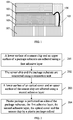
- FIG. 2 is a schematic flow diagram of a packaging method of an optical fingerprint sensor according to an embodiment of the present disclosure. It should be understood that FIG. 2 shows steps or operations of the packaging method, but these steps or operations are merely examples, and an embodiment of the present disclosure can also execute other operations or variations of the respective operations in FIG. 2 . In addition, steps in FIG. 2 may be executed in a different order as presented in FIG. 2 , and it is possible not to execute all the operations in FIG. 2 .
- a lower surface of a sensor chip and an upper surface of a package substrate are adhered using a first adhesive layer.
- the sensor chip and the package substrate are connected using a connection unit.
- a lower surface of an optical cover and an upper surface of the sensor chip are adhered using a second adhesive layer.
- Plastic package is performed on sides of the package substrate, the first adhesive layer, the second adhesive layer, the optical cover and the sensor chip by a plastic package colloid.
- optical fingerprint sensor packaged by using the packaging method in the embodiment of the present disclosure since an optical cover and a sensor chip are adhered together by the second adhesive layer, seamlessly and directly attachment of the optical cover and the sensor chip can be achieved, and a volume of the entire optical fingerprint sensor can be reduced, so that availability of the optical fingerprint sensor in an electronic device can be improved.
- the plastic package colloid when a plastic package is performed on the sides of the package substrate, the first adhesive layer, the second adhesive layer, the optical cover and the sensor chip by the plastic package colloid, the plastic package colloid shall expose an upper surface of the optical cover.
- the upper surface of the optical cover can be flush with an upper surface of the plastic package colloid, or the upper surface of the optical cover is higher than an upper surface of the plastic package colloid, whereas a height difference of the upper surface of the optical cover and the upper surface of the plastic package colloid is less than or equal to 50 microns.
- a side of the optical cover may have a screw thread or a lock type structure, so that the side of the optical cover can be attached to the plastic package colloid by camera lock process or other lock type processes.
- adhesion between the optical cover and the sensor chip can be enhanced, furthermore, reliability of an environmental test can be improved.
- the lower surface of the optical cover may completely cover a pixel area of the sensor chip, in other words, a size of the lower surface of the optical cover may be larger than a size of a pixel layout of the sensor chip, so as to reduce an influence on a yield of a broken pixel due to the overflow of an adhesive to the optical cover in the process of the plastic package.
- the optical fingerprint sensor shown in FIG. 1 can be obtained, that is, each technical feature in the optical fingerprint sensor shown in FIG. 1 is also applicable to the packaging method shown in FIG. 2 , which is not repeatedly described herein for brevity.
- the package substrate and the sensor chip can be adhered together using the first adhesive layer by a common die attaching process. Flatness between the package substrate and the sensor chip should be ensured as much as possible, to avoid affecting performance of the optical fingerprint sensor.
- the first adhesive layer can control a tilt between the package substrate and the sensor chip not exceeding 50 ⁇ m.
- the optical cover can be adhered to the sensor chip using the second adhesive layer by process similar to the die attaching process.
- Flatness and uniformity of the second adhesive layer can be ensured as much as possible.
- the flatness and the uniformity of the second adhesive layer can be achieved by controlling a thickness, a tilt, a filler, a hole, and the like of the second adhesive layer.
- the sensor chip and the package substrate being connected by the connection unit can be achieved by a wafer slot that controls a wire loop height or spin-coating process that controls stability of a wire loop on the lower surface of the sensor chip, or other processes.
- the lower surface of the sensor chip may be grinded, and selectively, a light blocking layer may be made on the grinded lower surface, such as a black silica gel layer or the like; alternatively, the colored target material may be accelerated and bombarded to the lower surface of the sensor chip, to form the light blocking layer; and alternatively, the light blocking layer can be generated on the lower surface of the sensor chip by screen printing, printing, spin-coating, electroplating, vacuum plating, or the like.
- a silicon dioxide layer that is, the optical cover
- the optical cover can be formed by means of spin-coating, or the optical cover, such as a glass sheet, a resin sheet or the like is produced by means of lamination processing, to avoid the sensor chip from damaging during processing or use.
- FIG. 3 is an exemplary structural diagram of an optical fingerprint sensor according to another embodiment of the present disclosure.
- An optical fingerprint sensor shown in FIG. 3 includes a plastic package colloid 103, a sensor chip 104, a connection unit 106, and a package substrate 107.
- a lower surface of the sensor chip 104 is adhered to an upper surface of the package substrate 107 by a first adhesive layer 105, the sensor chip 104 is connected to the package substrate 107 by the connection unit 106, and plastic package is performed on sides of the package substrate 107, the first adhesive layer 105 and the sensor chip 104 by a plastic package colloid 103. It should be noted that the plastic package colloid shall expose a pixel area of the sensor chip 104.
- the optical cover and the sensor chip can be seamlessly and directly attached, and a volume of the optical fingerprint sensor after being attached to the optical cover can be reduced, so that availability of the optical fingerprint sensor in an electronic device can be improved.
- the plastic package is performed on the sides of the package substrate 107, the first adhesive layer 105 and the sensor chip 104 by the plastic package colloid 103, which can protect the sensor chip.
- FIG. 3 Reference signs in FIG. 3 have the same or similar meanings as those in FIG. 1 , which are not described repeatedly herein for brevity.
- an upper surface of the plastic package colloid should be higher than an upper surface of the sensor chip so that after the upper surface of the sensor chip is attached to the optical cover, a surface of the optical cover can be flush with a surface of the plastic package colloid, or so that an upper surface of the optical cover is higher than the upper surface of the plastic package colloid, and a height difference of the upper surface of the optical cover and the upper surface of the plastic package colloid is less than or equal to 50 microns.
- FIG. 4 is a schematic flow diagram of a packaging method of an optical fingerprint sensor according to an embodiment of the present disclosure. It should be understood that FIG. 4 shows steps or operations of the packaging method, but these steps or operations are merely examples, and an embodiment of the present disclosure can also execute other operations or variations of the respective operations in FIG 4 . In addition, steps in FIG. 4 may be executed in a different order as presented in FIG. 4 , and it is possible not to execute all the operations in FIG. 4 .
- a lower surface of a sensor chip and an upper surface of a package substrate are adhered using a first adhesive layer.
- An output interface of a signal of the sensor chip and the package substrate are connected using a connection unit.
- Plastic package is performed on sides of the package substrate, the first adhesive layer and the sensor chip by a plastic package colloid. It should be noted that the plastic package colloid shall expose a pixel area of the sensor chip.
- an optical cover and the sensor chip can be seamlessly and directly attached, and a volume of the optical fingerprint sensor after being attached to the optical cover can be reduced, so that availability of the optical fingerprint sensor in an electronic device can be improved.
- An upper surface of the plastic package colloid should be higher than an upper surface of the sensor chip.
- the optical fingerprint sensor shown in FIG. 3 can be obtained.
- the steps that have the same reference signs as those in the packaging method shown in FIG. 2 indicate the same or similar meanings, which are not described repeatedly herein for brevity.
- a packaging method is further provided in the present disclosure, and as shown in FIG. 5 , a lower surface of an optical cover 101 is adhered to an upper surface of a sensor chip 104 by a second adhesive layer 102, to cover a pixel area.
- Reference signs in FIG. 5 have the same meanings as those in FIG. 3 , which are not described repeatedly herein.
- a height difference of an upper surface of the optical cover and an upper surface of a plastic package colloid may be greater than or equal to 0 and less than or equal to 50 microns.
Landscapes
- Engineering & Computer Science (AREA)
- Human Computer Interaction (AREA)
- Physics & Mathematics (AREA)
- General Physics & Mathematics (AREA)
- Multimedia (AREA)
- Theoretical Computer Science (AREA)
- Solid State Image Pick-Up Elements (AREA)
- Transforming Light Signals Into Electric Signals (AREA)
- Image Input (AREA)
- Measurement Of The Respiration, Hearing Ability, Form, And Blood Characteristics Of Living Organisms (AREA)
Abstract
Description
- The present disclosure relates to the field of electronic devices, and in particular, to an optical fingerprint sensor and a packaging method of an optical fingerprint sensor.
- With increasingly diverse demands for appearance of a fingerprint sensor by customers, the customers are not satisfied with a structure of a current through-hole fingerprint sensor, because the through-hole fingerprint sensor will change an appearance structure of a terminal. Although a blind-hole fingerprint sensor protects the appearance well, a poor yield and other issues caused by drilling a blind hole are also major problems.
- Although a penetration thickness of the optical fingerprint sensor can be more than 700 µm, a package thickness of a conventional optical fingerprint sensor is too thick to meet requirements of a smaller size for a fingerprint sensor.
- The present disclosure provides an optical fingerprint sensor and a packaging method of an optical fingerprint sensor, which can reduce a volume of the optical fingerprint sensor so that the optical fingerprint sensor can be better hidden in an electronic device.
- According to a first aspect, the present disclosure provides an optical fingerprint sensor, where the optical fingerprint sensor includes a package substrate, a sensor chip, an optical cover, a plastic package colloid and a connection unit, and the optical cover is light-transmissive; a lower surface of the sensor chip is adhered to an upper surface of the package substrate by a first adhesive layer, and a lower surface of the optical cover is adhered to an upper surface of the sensor chip by a second adhesive layer, the sensor ship is connected to the package substrate by the connection unit, plastic package is performed on sides of the package substrate, the first adhesive layer, the sensor chip, the second adhesive layer and the optical cover by the plastic package colloid, and the second adhesive layer is light-transmissive.
- According to the optical fingerprint sensor in an embodiment of the present disclosure, since the optical cover and the sensor chip are adhered together by the second adhesive layer, seamlessly and directly attachment of the optical cover and the sensor chip can be achieved, and a volume of the entire optical fingerprint sensor can be reduced, so that availability of the optical fingerprint sensor in an electronic device can be improved.
- In addition, the use of the plastic package colloid to perform the plastic package on the package substrate, the first adhesive layer, the sensor chip, the second adhesive layer and the optical cover can provide a protective effect.
- It should be noted that the plastic package colloid shall expose an upper surface of the optical cover.
- In a possible implementation, the plastic package colloid is opaque to light. This can improve the performance of the optical fingerprint sensor.
- In a possible implementation, a height difference of an upper surface of the optical cover and an upper surface of the plastic package colloid is greater than or equal to 0 and less than or equal to 50 microns. This can improve the performance of the optical fingerprint sensor.
- In a possible implementation, a side of the optical cover has a screw thread or a lock type structure.
- In a possible implementation, at least one of the package substrate, the first adhesive layer, and the lower surface of the sensor chip is opaque to light.
- In a possible implementation, the lower surface of the optical cover completely covers a pixel area of the sensor chip. In other words, a size of the optical cover is larger than a size of the pixel area of the sensor chip. This can improve the performance of the optical fingerprint sensor.
- In a possible implementation, the optical cover is a silicon dioxide layer formed by means of spin-coating, or a glass sheet or a resin sheet produced by means of lamination processing.
- According to a second aspect, the present disclosure provides a packaging method of an optical fingerprint sensor, where the optical fingerprint sensor includes a package substrate, a sensor chip, an optical cover, a plastic package colloid and a connection unit, the optical cover is light-transmissive, and the packaging method includes: adhering a lower surface of the sensor chip and an upper surface of the package substrate using a first adhesive layer; connecting the sensor chip and the package substrate using the connection unit; adhering a lower surface of the optical cover and an upper surface of the sensor chip using a second adhesive layer, where the second adhesive layer is light-transmissive; and performing plastic package on sides of the package substrate, the first adhesive layer, the sensor chip, the second adhesive layer and the optical cover using the plastic package colloid.
- According to the optical fingerprint sensor packaged by using the packaging method in an embodiment of the present disclosure, since the optical cover and the sensor chip are adhered together by the second adhesive layer, seamlessly and directly attachment of the optical cover and the sensor chip can be achieved, and a volume of the entire optical fingerprint sensor can be reduced, so that availability of the optical fingerprint sensor in an electronic device can be improved.
- In addition, the use of the plastic package colloid to perform the plastic package on the package substrate, the first adhesive layer, the sensor chip, the second adhesive layer and the optical cover can provide a protective effect.
- It should be noted that the plastic package colloid shall expose an upper surface of the optical cover.
- In a possible implementation, the plastic package colloid is opaque to light. This can improve the performance of the optical fingerprint sensor.
- In a possible implementation, a height difference of an upper surface of the optical cover and an upper surface of the plastic package colloid is greater than or equal to 0 and less than or equal to 50 microns. This can improve the performance of the optical fingerprint sensor.
- In a possible implementation, a side of the optical cover has a screw thread or a lock type structure.
- In a possible implementation, the lower surface of the optical cover completely covers a pixel area of the sensor chip. This can improve the performance of the optical fingerprint sensor.
- In a possible implementation, the optical cover is a silicon dioxide layer formed by means of spin-coating, or a glass sheet or a resin sheet produced by means of lamination processing.
- According to a third aspect, the present disclosure provides an optical fingerprint sensor. The optical fingerprint sensor includes a package substrate, a sensor chip, a plastic package colloid and a connection unit, and the optical cover is light-transmissive; a lower surface of the sensor chip is adhered to an upper surface of the package substrate by a first adhesive layer, the sensor ship is connected to the package substrate by the connection unit, plastic package is performed on sides of the package substrate, the first adhesive layer and the sensor chip by the plastic package colloid, and an upper surface of the plastic package colloid is higher than an upper surface of the sensor chip.
- According to the optical fingerprint sensor in an embodiment of the present disclosure, the optical cover and the sensor chip are adhered together by a second adhesive layer, and therefore seamlessly and directly attachment of the optical cover and the sensor chip can be achieved, and a volume of the optical fingerprint sensor after installing the optical cover can be reduced, so that availability of the optical fingerprint sensor in an electronic device can be improved.
- In addition, the use of the plastic package colloid to perform the plastic package on the package substrate, the first adhesive layer and the sensor chip can provide a protective effect.
- It should be noted that the plastic package colloid shall expose the pixel area of the sensor chip.
- In a possible implementation, the plastic package colloid is opaque to light. This can improve the performance of the optical fingerprint sensor.
- In a possible implementation, at least one of the package substrate, the first adhesive layer, and the lower surface of the sensor chip is opaque to light. This can improve the performance of the optical fingerprint sensor.
- According to a fourth aspect, the present disclosure provides a packaging method of an optical fingerprint sensor, where the optical fingerprint sensor includes a package substrate, a sensor chip, a plastic package colloid and a connection unit, and the packaging method includes: adhering a lower surface of the sensor chip and an upper surface of the package substrate using a first adhesive layer; connecting the sensor chip and the package substrate using the connection unit; and performing plastic package on sides of the package substrate, the first adhesive layer and the sensor chip using the plastic package colloid, where an upper surface of the plastic package colloid is higher than an upper surface of the sensor chip.
- According to the optical fingerprint sensor packaged by using the packaging method in an embodiment of the present disclosure, the optical cover and the sensor chip are adhered together by the second adhesive layer, and therefore seamlessly and directly attachment of the optical cover and the sensor chip can be achieved, and a volume of the optical fingerprint sensor after installing the optical cover can be reduced, so that availability of the optical fingerprint sensor in an electronic device can be improved.
- In addition, the use of the plastic package colloid to perform the plastic package on the package substrate, the first adhesive layer and the sensor chip can provide a protective effect.
- It should be noted that the plastic package colloid shall expose the pixel area of the sensor chip.
- In a possible implementation, the plastic package colloid is opaque to light.
- In a possible implementation, at least one of the package substrate, the first adhesive layer, and the lower surface of the sensor chip is opaque to light.
- According to a fifth aspect, the present disclosure provides a packaging method of an optical fingerprint sensor, where the optical fingerprint sensor is the optical fingerprint sensor according to the third aspect or any one of the possible implementations, and the packaging method includes: adhering a lower surface of an optical cover to the upper surface of the sensor chip of the optical fingerprint sensor using a second adhesive layer.
- According to the optical fingerprint sensor packaged by using the packaging method in an embodiment of the present disclosure, the optical cover and the sensor chip are adhered together by the second adhesive layer, and therefore seamlessly and directly attachment of the optical cover and the sensor chip can be achieved, and a volume of the optical fingerprint sensor after installing the optical cover can be reduced, so that availability of the optical fingerprint sensor in an electronic device can be improved.
- In a possible implementation, a height difference of an upper surface of the optical cover and the upper surface of the plastic package colloid of the optical fingerprint sensor is greater than or equal to 0 and less than or equal to 50 microns.
-
-
FIG. 1 is an exemplary structural diagram of an optical fingerprint sensor according to an embodiment of the present disclosure; -
FIG. 2 is a schematic flow diagram of a packaging method of an optical fingerprint sensor according to an embodiment of the present disclosure; -
FIG. 3 is an exemplary structural diagram of an optical fingerprint sensor according to another embodiment of the present disclosure; -
FIG. 4 is a schematic flow diagram of a packaging method of an optical fingerprint sensor according to another embodiment of the present disclosure; and -
FIG. 5 is a schematic flow diagram of a packaging method of an optical fingerprint sensor according to yet another embodiment of the present disclosure. - As shown in
FIG. 1 , in an embodiment of the present disclosure, an optical fingerprint sensor includes anoptical cover 101, a plastic package colloid 103, asensor chip 104, aconnection unit 106, and apackage substrate 107. - A lower surface of the
optical cover 101 and an upper surface of thesensor chip 104 are adhered together by a secondadhesive layer 102, a lower surface of thesensor chip 104 and an upper surface of thepackage substrate 107 are adhered together by a firstadhesive layer 105, thesensor chip 104 and thepackage substrate 107 are connected by theconnection unit 106, and plastic package is performed on sides of thepackage substrate 107, the firstadhesive layer 105, thesensor chip 104, the secondadhesive layer 102 and theoptical cover 101 by the plastic package colloid 103. - It should be noted that the
plastic package colloid 103 shall expose an upper surface of theoptical cover 101. - The
optical cover 101 is light-transmissive. The optical cover can also be used to amplify a transmitted light signal. The optical cover can also be used to protect the sensor chip, and in this case, the optical cover can also be referred to as a protective layer. - The
package substrate 107 is used to carry thesensor chip 104 and connect a signal of thesensor chip 104 to the outside. In addition, thepackage substrate 107 can also provide protective and heat dissipation functions. - The
connection unit 106 is used to transmit an electric signal output by thesensor chip 101 to thepackage substrate 107. - Except for features of a plastic package colloid used in a general packaging, the
plastic package colloid 103 may also have a light blocking property, that is, theplastic package colloid 103 is opaque to light. - The
sensor chip 104 is used to receive light reflected from a finger of a user and convert the reflected light into an image to identify a fingerprint of the user. - According to the optical fingerprint sensor in the embodiment of the present disclosure, since an optical cover and a sensor chip are adhered together by the second adhesive layer, seamlessly and directly attachment of the optical cover and the sensor chip can be achieved, and a volume of the entire optical fingerprint sensor can be reduced, so that availability of the optical fingerprint sensor in an electronic device can be improved.
- In addition, the use of a plastic package colloid to perform the plastic package on the sensor chip, the package substrate and the optical cover can provide a protective effect.
- As illustrated in
FIG. 1 , an upper surface of the optical cover is higher than an upper surface of the plastic package colloid, and a height difference thereof generally cannot exceed 50 µm. Optionally, the upper surface of the optical cover can also be flush with the upper surface of the plastic package colloid. - The first
adhesive layer 105 may be an adhesive layer formed by uniformly coating and curing of an organic adhesive (such as an epoxy adhesive), and may also be an adhesive film. - The second
adhesive layer 102 may be an organic solid adhesive with a high light transmittance, and the optical cover and the sensor chip may be evenly adhered to the uniform second adhesive layer by process similar to die attaching process. The second adhesive layer, to the greatest extent, does not contain bubbles, voids and the like that affect uniformity. - The second adhesive layer is transmissive, so that the light transmitted through the optical cover can reach the sensor chip.
- In general, the second adhesive layer has a good adhesive property as much as possible, which can stably adhere the optical cover to the sensor chip. A thickness of the second adhesive layer is also better not to exceed 50 microns. A tilt of the optical cover with respect to the sensor chip is better not to exceed 50 µm, and a light-transmissive range of the second adhesive layer should cover a visible light waveband as much as possible.
- Optionally, the package substrate may be a metal frame, a flexible circuit board, a flexible and rigid printed circuit board, or a printed circuit board used for package.
- Optionally, the package substrate may have a light blocking effect, that is, it is opaque to light. The package substrate is opaque to light for example, by filling a via, printing a black solder mask, or the like.
- Optionally, the lower surface of the sensor chip is opaque to light. Specifically, the lower surface of the sensor chip may be covered with a light blocking layer, such as a black silica gel layer.
- The light blocking layer can be generated by screen printing, printing, spin-coating, electroplating, vacuum plating, or the like. Alternatively, the lower surface of the sensor chip may be grinded, and further, the light blocking layer may be made on the grinded lower surface. Alternatively, colored target material may be accelerated and bombarded to the lower surface of the sensor chip, to form the light blocking layer.
- Optionally, the first adhesive layer may have a light blocking effect, that is, it is opaque to light.
- Optionally, the lower surface of the sensor chip and the upper surface of the package substrate may be evenly adhered together by the first adhesive layer to avoid light refraction. Specifically, after the sensor chip and the package substrate are adhered together by the first adhesive layer, a tilt of the sensor chip with respect to the package substrate does not exceed 50 µm, so as to avoid affecting the performance of fingerprint detection.
- Optionally, the connection unit may include a metal bonding wire, a gold wire or a copper wire, a metal bump, a rewiring line, a flexible circuit lamination connection, or the like.
- Optionally, the lower surface of the sensor chip may have a slot that controls a wire loop height, the connection unit passes through the slot, and then is connected to the package substrate.
- Optionally, the connection unit can be realized by spin-coating process that controls stability of a wire loop or other processes.
- Optionally, the optical cover may be a silicon dioxide layer formed by means of spin-coating, or a glass sheet or a resin sheet produced by means of lamination processing, to avoid the sensor chip from damaging during processing or use.
- Optionally, the lower surface of the optical cover may completely cover a pixel area of the sensor chip, in other words, a size of the lower surface of the optical cover may be larger than a size of a pixel layout of the sensor chip, the sensor chip.
- Optionally, in the optical fingerprint sensor shown in
FIG. 1 , a side of the optical cover may have a screw thread. Alternatively, a side of the optical cover may include a lock type structure, so that the side of the optical cover can be attached to the plastic package colloid by a camera lock process or other lock type processes. Thus, adhesion between the optical cover and the sensor chip can be enhanced, furthermore, reliability of an environmental test can be improved. -
FIG. 2 is a schematic flow diagram of a packaging method of an optical fingerprint sensor according to an embodiment of the present disclosure. It should be understood thatFIG. 2 shows steps or operations of the packaging method, but these steps or operations are merely examples, and an embodiment of the present disclosure can also execute other operations or variations of the respective operations inFIG. 2 . In addition, steps inFIG. 2 may be executed in a different order as presented inFIG. 2 , and it is possible not to execute all the operations inFIG. 2 . - S201. A lower surface of a sensor chip and an upper surface of a package substrate are adhered using a first adhesive layer.
- S202. The sensor chip and the package substrate are connected using a connection unit.
- S203. A lower surface of an optical cover and an upper surface of the sensor chip are adhered using a second adhesive layer.
- S204. Plastic package is performed on sides of the package substrate, the first adhesive layer, the second adhesive layer, the optical cover and the sensor chip by a plastic package colloid.
- According to the optical fingerprint sensor packaged by using the packaging method in the embodiment of the present disclosure, since an optical cover and a sensor chip are adhered together by the second adhesive layer, seamlessly and directly attachment of the optical cover and the sensor chip can be achieved, and a volume of the entire optical fingerprint sensor can be reduced, so that availability of the optical fingerprint sensor in an electronic device can be improved.
- It should be noted that when a plastic package is performed on the sides of the package substrate, the first adhesive layer, the second adhesive layer, the optical cover and the sensor chip by the plastic package colloid, the plastic package colloid shall expose an upper surface of the optical cover.
- The upper surface of the optical cover can be flush with an upper surface of the plastic package colloid, or the upper surface of the optical cover is higher than an upper surface of the plastic package colloid, whereas a height difference of the upper surface of the optical cover and the upper surface of the plastic package colloid is less than or equal to 50 microns.
- Optionally, a side of the optical cover may have a screw thread or a lock type structure, so that the side of the optical cover can be attached to the plastic package colloid by camera lock process or other lock type processes. Thus, adhesion between the optical cover and the sensor chip can be enhanced, furthermore, reliability of an environmental test can be improved.
- Optionally, the lower surface of the optical cover may completely cover a pixel area of the sensor chip, in other words, a size of the lower surface of the optical cover may be larger than a size of a pixel layout of the sensor chip, so as to reduce an influence on a yield of a broken pixel due to the overflow of an adhesive to the optical cover in the process of the plastic package.
- According to the packaging method of the embodiment of the present disclosure, the optical fingerprint sensor shown in
FIG. 1 can be obtained, that is, each technical feature in the optical fingerprint sensor shown inFIG. 1 is also applicable to the packaging method shown inFIG. 2 , which is not repeatedly described herein for brevity. - In S201, the package substrate and the sensor chip can be adhered together using the first adhesive layer by a common die attaching process. Flatness between the package substrate and the sensor chip should be ensured as much as possible, to avoid affecting performance of the optical fingerprint sensor.
- Specifically, the first adhesive layer can control a tilt between the package substrate and the sensor chip not exceeding 50 µm.
- In S203, the optical cover can be adhered to the sensor chip using the second adhesive layer by process similar to the die attaching process. Flatness and uniformity of the second adhesive layer can be ensured as much as possible. For example, the flatness and the uniformity of the second adhesive layer can be achieved by controlling a thickness, a tilt, a filler, a hole, and the like of the second adhesive layer.
- In S202, the sensor chip and the package substrate being connected by the connection unit can be achieved by a wafer slot that controls a wire loop height or spin-coating process that controls stability of a wire loop on the lower surface of the sensor chip, or other processes.
- Optionally, in an embodiment of the present disclosure, the lower surface of the sensor chip may be grinded, and selectively, a light blocking layer may be made on the grinded lower surface, such as a black silica gel layer or the like; alternatively, the colored target material may be accelerated and bombarded to the lower surface of the sensor chip, to form the light blocking layer; and alternatively, the light blocking layer can be generated on the lower surface of the sensor chip by screen printing, printing, spin-coating, electroplating, vacuum plating, or the like.
- Optionally, in an embodiment of the present disclosure, a silicon dioxide layer, that is, the optical cover, can be formed by means of spin-coating, or the optical cover, such as a glass sheet, a resin sheet or the like is produced by means of lamination processing, to avoid the sensor chip from damaging during processing or use.
-
FIG. 3 is an exemplary structural diagram of an optical fingerprint sensor according to another embodiment of the present disclosure. An optical fingerprint sensor shown inFIG. 3 includes aplastic package colloid 103, asensor chip 104, aconnection unit 106, and apackage substrate 107. - A lower surface of the
sensor chip 104 is adhered to an upper surface of thepackage substrate 107 by a firstadhesive layer 105, thesensor chip 104 is connected to thepackage substrate 107 by theconnection unit 106, and plastic package is performed on sides of thepackage substrate 107, the firstadhesive layer 105 and thesensor chip 104 by aplastic package colloid 103. It should be noted that the plastic package colloid shall expose a pixel area of thesensor chip 104. - According to the optical fingerprint sensor in the embodiment of the present disclosure, during a subsequent package process, the optical cover and the sensor chip can be seamlessly and directly attached, and a volume of the optical fingerprint sensor after being attached to the optical cover can be reduced, so that availability of the optical fingerprint sensor in an electronic device can be improved.
- In addition, the plastic package is performed on the sides of the
package substrate 107, the firstadhesive layer 105 and thesensor chip 104 by theplastic package colloid 103, which can protect the sensor chip. - Reference signs in
FIG. 3 have the same or similar meanings as those inFIG. 1 , which are not described repeatedly herein for brevity. - It should be noted that an upper surface of the plastic package colloid should be higher than an upper surface of the sensor chip so that after the upper surface of the sensor chip is attached to the optical cover, a surface of the optical cover can be flush with a surface of the plastic package colloid, or so that an upper surface of the optical cover is higher than the upper surface of the plastic package colloid, and a height difference of the upper surface of the optical cover and the upper surface of the plastic package colloid is less than or equal to 50 microns.
-
FIG. 4 is a schematic flow diagram of a packaging method of an optical fingerprint sensor according to an embodiment of the present disclosure. It should be understood thatFIG. 4 shows steps or operations of the packaging method, but these steps or operations are merely examples, and an embodiment of the present disclosure can also execute other operations or variations of the respective operations inFIG 4 . In addition, steps inFIG. 4 may be executed in a different order as presented inFIG. 4 , and it is possible not to execute all the operations inFIG. 4 . - S201. A lower surface of a sensor chip and an upper surface of a package substrate are adhered using a first adhesive layer.
- S202. An output interface of a signal of the sensor chip and the package substrate are connected using a connection unit.
- S205. Plastic package is performed on sides of the package substrate, the first adhesive layer and the sensor chip by a plastic package colloid. It should be noted that the plastic package colloid shall expose a pixel area of the sensor chip.
- According to the optical fingerprint sensor packaged by using the packaging method in the embodiment of the present disclosure, an optical cover and the sensor chip can be seamlessly and directly attached, and a volume of the optical fingerprint sensor after being attached to the optical cover can be reduced, so that availability of the optical fingerprint sensor in an electronic device can be improved.
- An upper surface of the plastic package colloid should be higher than an upper surface of the sensor chip.
- According to the packaging method of the embodiment of the present disclosure, the optical fingerprint sensor shown in
FIG. 3 can be obtained. In the packaging method of the embodiment of the present disclosure, the steps that have the same reference signs as those in the packaging method shown inFIG. 2 indicate the same or similar meanings, which are not described repeatedly herein for brevity. - A packaging method is further provided in the present disclosure, and as shown in
FIG. 5 , a lower surface of anoptical cover 101 is adhered to an upper surface of asensor chip 104 by a secondadhesive layer 102, to cover a pixel area. Reference signs inFIG. 5 have the same meanings as those inFIG. 3 , which are not described repeatedly herein. - A height difference of an upper surface of the optical cover and an upper surface of a plastic package colloid may be greater than or equal to 0 and less than or equal to 50 microns.
Claims (22)
- An optical fingerprint sensor, wherein the optical fingerprint sensor comprises a package substrate, a sensor chip, an optical cover, a plastic package colloid and a connection unit, and the optical cover is light-transmissive;
a lower surface of the sensor chip is adhered to an upper surface of the package substrate by a first adhesive layer, and a lower surface of the optical cover is adhered to an upper surface of the sensor chip by a second adhesive layer, the sensor ship is connected to the package substrate by the connection unit, plastic package is performed on sides of the package substrate, the first adhesive layer, the sensor chip, the second adhesive layer and the optical cover by the plastic package colloid, and the second adhesive layer is light-transmissive. - The optical fingerprint sensor according to claim 1, wherein the plastic package colloid is opaque to light.
- The optical fingerprint sensor according to claim 1, wherein a height difference of an upper surface of the optical cover and an upper surface of the plastic package colloid is greater than or equal to 0 and less than or equal to 50 microns.
- The optical fingerprint sensor according to any one of claims 1 to 3, wherein a side of the optical cover has a screw thread or a lock type structure.
- The optical fingerprint sensor according to any one of claims 1 to 3, wherein the lower surface of the optical cover completely covers a pixel area of the sensor chip.
- The optical fingerprint sensor according to any one of claims 1 to 3, wherein the optical cover is a silicon dioxide layer formed by means of spin-coating, or a glass sheet or a resin sheet produced by means of lamination processing.
- The optical fingerprint sensor according to any one of claims 1 to 3, wherein at least one of the package substrate, the first adhesive layer, and the lower surface of the sensor chip is opaque to light.
- A packaging method of an optical fingerprint sensor, wherein the optical fingerprint sensor comprises a package substrate, a sensor chip, an optical cover, a plastic package colloid and a connection unit, the optical cover is light-transmissive, and the packaging method comprises:adhering a lower surface of the sensor chip and an upper surface of the package substrate using a first adhesive layer;connecting the sensor chip and the package substrate using the connection unit;adhering a lower surface of the optical cover and an upper surface of the sensor chip using a second adhesive layer, wherein the second adhesive layer is light-transmissive; andperforming plastic package on sides of the package substrate, the first adhesive layer, the sensor chip, the second adhesive layer and the optical cover using the plastic package colloid.
- The packaging method according to claim 8, wherein the plastic package colloid is opaque to light.
- The packaging method according to claim 8, wherein a height difference of an upper surface of the optical cover and an upper surface of the plastic package colloid is greater than or equal to 0 and less than or equal to 50 microns.
- The packaging method according to any one of claims 8 to 10, wherein a side of the optical cover has a screw thread or a lock type structure.
- The packaging method according to any one of claims 8 to 10, wherein the lower surface of the optical cover completely covers a pixel area of the sensor chip.
- The packaging method according to any one of claims 8 to 10, wherein the optical cover is a silicon dioxide layer formed by means of spin-coating, or a glass sheet or a resin sheet produced by means of lamination processing.
- The packaging method according to any one of claims 8 to 10, wherein at least one of the package substrate, the first adhesive layer, and the lower surface of the sensor chip is opaque to light.
- An optical fingerprint sensor, wherein the optical fingerprint sensor comprises a package substrate, a sensor chip, a plastic package colloid and a connection unit, and the optical cover is light-transmissive;
a lower surface of the sensor chip is adhered to an upper surface of the package substrate by a first adhesive layer, the sensor ship is connected to the package substrate by the connection unit, plastic package is performed on sides of the package substrate, the first adhesive layer and the sensor chip by the plastic package colloid, and an upper surface of the plastic package colloid is higher than an upper surface of the sensor chip. - The optical fingerprint sensor according to claim 15, wherein the plastic package colloid is opaque to light.
- The optical fingerprint sensor according to any one of claim 15 or 16, wherein at least one of the package substrate, the first adhesive layer, and the lower surface of the sensor chip is opaque to light.
- A packaging method of an optical fingerprint sensor, wherein the optical fingerprint sensor comprises a package substrate, a sensor chip, a plastic package colloid and a connection unit, and the packaging method comprises:adhering a lower surface of the sensor chip and an upper surface of the package substrate using a first adhesive layer;connecting the sensor chip and the package substrate using the connection unit; andperforming plastic package on sides of the package substrate, the first adhesive layer and the sensor chip using the plastic package colloid, wherein an upper surface of the plastic package colloid is higher than an upper surface of the sensor chip.
- The packaging method according to claim 18, wherein the plastic package colloid is opaque to light.
- The packaging method according to claim 18, wherein at least one of the package substrate, the first adhesive layer, and the lower surface of the sensor chip is opaque to light.
- A packaging method of an optical fingerprint sensor, wherein the optical fingerprint sensor is the optical fingerprint sensor according to any one of claims 15 to 17, and the packaging method comprises:
adhering a lower surface of an optical cover to the upper surface of the sensor chip of the optical fingerprint sensor using a second adhesive layer. - The packaging method according to claim 21, wherein a height difference of an upper surface of the optical cover and the upper surface of the plastic package colloid of the optical fingerprint sensor is greater than or equal to 0 and less than or equal to 50 microns.
Applications Claiming Priority (1)
| Application Number | Priority Date | Filing Date | Title |
|---|---|---|---|
| PCT/CN2017/080229 WO2018187963A1 (en) | 2017-04-12 | 2017-04-12 | Optical fingerprint sensor and packaging method therefor |
Publications (2)
| Publication Number | Publication Date |
|---|---|
| EP3428837A1 true EP3428837A1 (en) | 2019-01-16 |
| EP3428837A4 EP3428837A4 (en) | 2019-05-15 |
Family
ID=63344746
Family Applications (1)
| Application Number | Title | Priority Date | Filing Date |
|---|---|---|---|
| EP17904357.5A Pending EP3428837A4 (en) | 2017-04-12 | 2017-04-12 | OPTICAL DIGITAL FOOTPRINT SENSOR AND PACKING METHOD THEREOF |
Country Status (4)
| Country | Link |
|---|---|
| US (1) | US20190026525A1 (en) |
| EP (1) | EP3428837A4 (en) |
| CN (1) | CN108496179A (en) |
| WO (1) | WO2018187963A1 (en) |
Families Citing this family (8)
| Publication number | Priority date | Publication date | Assignee | Title |
|---|---|---|---|---|
| WO2020087535A1 (en) * | 2018-11-02 | 2020-05-07 | 深圳市汇顶科技股份有限公司 | Liveness recognition apparatus and door lock |
| KR20250026412A (en) * | 2019-01-18 | 2025-02-25 | 트리나미엑스 게엠베하 | Optical sensor and detector for an optical detection |
| CN111276450A (en) * | 2020-02-22 | 2020-06-12 | 多感科技(上海)有限公司 | Chip module and method of forming the same |
| CN111883440B (en) * | 2020-07-30 | 2022-10-18 | 青岛歌尔微电子研究院有限公司 | Glue filling method, module packaging structure and electronic equipment |
| CN114078979A (en) * | 2020-08-20 | 2022-02-22 | 昇佳电子股份有限公司 | The structure of the optical sensor |
| WO2022047761A1 (en) * | 2020-09-06 | 2022-03-10 | 深圳市汇顶科技股份有限公司 | Chip processing method and system, chip, and device |
| CN113511628A (en) * | 2021-08-10 | 2021-10-19 | 华天科技(西安)有限公司 | Manufacturing method of MEMS product based on grinding process |
| CN117083645B (en) | 2022-02-23 | 2026-02-10 | 京东方科技集团股份有限公司 | fingerprint recognition module |
Family Cites Families (19)
| Publication number | Priority date | Publication date | Assignee | Title |
|---|---|---|---|---|
| US5216278A (en) * | 1990-12-04 | 1993-06-01 | Motorola, Inc. | Semiconductor device having a pad array carrier package |
| US6995462B2 (en) * | 2003-09-17 | 2006-02-07 | Micron Technology, Inc. | Image sensor packages |
| US7645635B2 (en) * | 2004-08-16 | 2010-01-12 | Micron Technology, Inc. | Frame structure and semiconductor attach process for use therewith for fabrication of image sensor packages and the like, and resulting packages |
| JP4825538B2 (en) * | 2006-02-17 | 2011-11-30 | 富士通セミコンダクター株式会社 | Manufacturing method of semiconductor device |
| TWI305036B (en) * | 2006-09-28 | 2009-01-01 | Siliconware Precision Industries Co Ltd | Sensor-type package structure and fabrication method thereof |
| US9754913B2 (en) * | 2013-10-18 | 2017-09-05 | Sencio B.V. | Integrated circuit package |
| TWI575779B (en) * | 2014-03-31 | 2017-03-21 | 精材科技股份有限公司 | Chip package and method of manufacturing same |
| TWI531980B (en) * | 2015-01-19 | 2016-05-01 | 致伸科技股份有限公司 | A method of producing sensing device |
| CN104779223A (en) * | 2015-04-10 | 2015-07-15 | 华进半导体封装先导技术研发中心有限公司 | Fingerprint identification chip packaging structure provided with unilateral groove and manufacturing method |
| CN104850840A (en) * | 2015-05-19 | 2015-08-19 | 苏州晶方半导体科技股份有限公司 | Chip packaging method and chip packaging structure |
| KR20160143071A (en) * | 2015-06-04 | 2016-12-14 | 앰코 테크놀로지 코리아 주식회사 | Package of finger print sensor |
| CN205003690U (en) * | 2015-08-27 | 2016-01-27 | 广东欧珀移动通信有限公司 | Fingerprint recognition sensor encapsulation structure |
| CN106601629B (en) * | 2015-10-15 | 2018-11-30 | 力成科技股份有限公司 | Chip packaging structure with protective sheet adhered to chip induction surface |
| CN105304575B (en) * | 2015-10-23 | 2019-04-23 | 华天科技(西安)有限公司 | Using the inclined encapsulating structure of cushion block prevention fingerprint sensor and manufacturing method |
| CN105529308B (en) * | 2015-11-09 | 2019-10-25 | 华天科技(西安)有限公司 | A fingerprint chip package structure and manufacturing method with spacer and bottom filling |
| TW201730809A (en) * | 2016-02-19 | 2017-09-01 | 致伸科技股份有限公司 | Fingerprint identification module and manufacturing method thereof |
| US10536568B2 (en) * | 2016-07-01 | 2020-01-14 | Huawei Technologies Co., Ltd. | Waterproof fingerprint recognition module and electronic device |
| CN106098644A (en) * | 2016-08-11 | 2016-11-09 | 华天科技(西安)有限公司 | Chip-packaging structure that a kind of DAF film is combined with cushion block and manufacture method thereof |
| CN108205650B (en) * | 2016-12-20 | 2021-11-30 | 致伸科技股份有限公司 | Fingerprint identification module |
-
2017
- 2017-04-12 CN CN201780006049.XA patent/CN108496179A/en active Pending
- 2017-04-12 EP EP17904357.5A patent/EP3428837A4/en active Pending
- 2017-04-12 WO PCT/CN2017/080229 patent/WO2018187963A1/en not_active Ceased
-
2018
- 2018-09-25 US US16/140,533 patent/US20190026525A1/en not_active Abandoned
Also Published As
| Publication number | Publication date |
|---|---|
| CN108496179A (en) | 2018-09-04 |
| EP3428837A4 (en) | 2019-05-15 |
| US20190026525A1 (en) | 2019-01-24 |
| WO2018187963A1 (en) | 2018-10-18 |
Similar Documents
| Publication | Publication Date | Title |
|---|---|---|
| US20190026525A1 (en) | Optical fingerprint sensor and packaging method of optical fingerprint sensor | |
| US8605211B2 (en) | Low rise camera module | |
| US20230290699A1 (en) | Sensor package and manufacturing method thereof | |
| CN206931604U (en) | Optical fingerprint sensor | |
| US10061965B2 (en) | Fingerprint sensing unit and fingerprint sensing module | |
| US10126462B2 (en) | Proximity sensor, electronic apparatus and method for manufacturing proximity sensor | |
| US11646331B2 (en) | Package substrate | |
| US10461066B2 (en) | Structure and method for hybrid optical package with glass top cover | |
| US20100025793A1 (en) | Assembly for image sensing chip and assembling method thereof | |
| CN109196657A (en) | Optical module, module and its manufacturing method | |
| JP2014175465A (en) | Semiconductor device, manufacturing method, electronic device | |
| US11049899B2 (en) | Encapsulation structure of image sensing chip, and encapsulation method therefor | |
| CN106897712A (en) | Fingerprint module, display screen and mobile terminal | |
| CN109417081B (en) | Chip packaging structure, method and electronic equipment | |
| WO2017174007A1 (en) | Chip packaging structure, terminal device, and method | |
| JP6971826B2 (en) | Solid-state image sensor and its manufacturing method | |
| US10244638B2 (en) | Proximity sensor and manufacturing method therefor | |
| US20080122059A1 (en) | Stacked chip package structure and fabricating method thereof | |
| US10541264B2 (en) | Package-on-package structure and package-on-package method | |
| WO2017088729A1 (en) | Image sensing chip packaging structure and method | |
| CN100454505C (en) | Semiconductor device and method for fabricating the same | |
| US20210104563A1 (en) | Ultra-thin package structure for integrated circuit having sensing function and method forming the same | |
| JP2003209332A (en) | Printed wiring board, method for manufacturing printed wiring board, and mounting board | |
| CN113299706A (en) | Display panel and display device | |
| US20080303111A1 (en) | Sensor package and method for fabricating the same |
Legal Events
| Date | Code | Title | Description |
|---|---|---|---|
| STAA | Information on the status of an ep patent application or granted ep patent |
Free format text: STATUS: UNKNOWN |
|
| STAA | Information on the status of an ep patent application or granted ep patent |
Free format text: STATUS: THE INTERNATIONAL PUBLICATION HAS BEEN MADE |
|
| PUAI | Public reference made under article 153(3) epc to a published international application that has entered the european phase |
Free format text: ORIGINAL CODE: 0009012 |
|
| STAA | Information on the status of an ep patent application or granted ep patent |
Free format text: STATUS: REQUEST FOR EXAMINATION WAS MADE |
|
| 17P | Request for examination filed |
Effective date: 20181010 |
|
| AK | Designated contracting states |
Kind code of ref document: A1 Designated state(s): AL AT BE BG CH CY CZ DE DK EE ES FI FR GB GR HR HU IE IS IT LI LT LU LV MC MK MT NL NO PL PT RO RS SE SI SK SM TR |
|
| AX | Request for extension of the european patent |
Extension state: BA ME |
|
| RIC1 | Information provided on ipc code assigned before grant |
Ipc: H01L 23/10 20060101ALI20190201BHEP Ipc: H01L 21/50 20060101ALI20190201BHEP Ipc: G06K 9/00 20060101AFI20190201BHEP |
|
| R17P | Request for examination filed (corrected) |
Effective date: 20181010 |
|
| A4 | Supplementary search report drawn up and despatched |
Effective date: 20190411 |
|
| RIC1 | Information provided on ipc code assigned before grant |
Ipc: H01L 23/10 20060101ALI20190405BHEP Ipc: G06K 9/00 20060101AFI20190405BHEP Ipc: H01L 27/146 20060101ALI20190405BHEP Ipc: H01L 21/50 20060101ALI20190405BHEP Ipc: H01L 23/31 20060101ALI20190405BHEP Ipc: H01L 21/56 20060101ALI20190405BHEP |
|
| STAA | Information on the status of an ep patent application or granted ep patent |
Free format text: STATUS: EXAMINATION IS IN PROGRESS |
|
| 17Q | First examination report despatched |
Effective date: 20200113 |
|
| DAV | Request for validation of the european patent (deleted) | ||
| DAX | Request for extension of the european patent (deleted) |