EP3428525A1 - Flash light source device - Google Patents
Flash light source device Download PDFInfo
- Publication number
- EP3428525A1 EP3428525A1 EP17762740.3A EP17762740A EP3428525A1 EP 3428525 A1 EP3428525 A1 EP 3428525A1 EP 17762740 A EP17762740 A EP 17762740A EP 3428525 A1 EP3428525 A1 EP 3428525A1
- Authority
- EP
- European Patent Office
- Prior art keywords
- housing
- electromagnetic shield
- opening
- shield layer
- light source
- Prior art date
- Legal status (The legal status is an assumption and is not a legal conclusion. Google has not performed a legal analysis and makes no representation as to the accuracy of the status listed.)
- Withdrawn
Links
Images





Classifications
-
- F—MECHANICAL ENGINEERING; LIGHTING; HEATING; WEAPONS; BLASTING
- F21—LIGHTING
- F21S—NON-PORTABLE LIGHTING DEVICES; SYSTEMS THEREOF; VEHICLE LIGHTING DEVICES SPECIALLY ADAPTED FOR VEHICLE EXTERIORS
- F21S10/00—Lighting devices or systems producing a varying lighting effect
- F21S10/06—Lighting devices or systems producing a varying lighting effect flashing, e.g. with rotating reflector or light source
-
- F—MECHANICAL ENGINEERING; LIGHTING; HEATING; WEAPONS; BLASTING
- F21—LIGHTING
- F21V—FUNCTIONAL FEATURES OR DETAILS OF LIGHTING DEVICES OR SYSTEMS THEREOF; STRUCTURAL COMBINATIONS OF LIGHTING DEVICES WITH OTHER ARTICLES, NOT OTHERWISE PROVIDED FOR
- F21V23/00—Arrangement of electric circuit elements in or on lighting devices
-
- F—MECHANICAL ENGINEERING; LIGHTING; HEATING; WEAPONS; BLASTING
- F21—LIGHTING
- F21V—FUNCTIONAL FEATURES OR DETAILS OF LIGHTING DEVICES OR SYSTEMS THEREOF; STRUCTURAL COMBINATIONS OF LIGHTING DEVICES WITH OTHER ARTICLES, NOT OTHERWISE PROVIDED FOR
- F21V23/00—Arrangement of electric circuit elements in or on lighting devices
- F21V23/003—Arrangement of electric circuit elements in or on lighting devices the elements being electronics drivers or controllers for operating the light source, e.g. for a LED array
- F21V23/004—Arrangement of electric circuit elements in or on lighting devices the elements being electronics drivers or controllers for operating the light source, e.g. for a LED array arranged on a substrate, e.g. a printed circuit board
-
- F—MECHANICAL ENGINEERING; LIGHTING; HEATING; WEAPONS; BLASTING
- F21—LIGHTING
- F21V—FUNCTIONAL FEATURES OR DETAILS OF LIGHTING DEVICES OR SYSTEMS THEREOF; STRUCTURAL COMBINATIONS OF LIGHTING DEVICES WITH OTHER ARTICLES, NOT OTHERWISE PROVIDED FOR
- F21V25/00—Safety devices structurally associated with lighting devices
-
- G—PHYSICS
- G03—PHOTOGRAPHY; CINEMATOGRAPHY; ANALOGOUS TECHNIQUES USING WAVES OTHER THAN OPTICAL WAVES; ELECTROGRAPHY; HOLOGRAPHY
- G03B—APPARATUS OR ARRANGEMENTS FOR TAKING PHOTOGRAPHS OR FOR PROJECTING OR VIEWING THEM; APPARATUS OR ARRANGEMENTS EMPLOYING ANALOGOUS TECHNIQUES USING WAVES OTHER THAN OPTICAL WAVES; ACCESSORIES THEREFOR
- G03B15/00—Special procedures for taking photographs; Apparatus therefor
- G03B15/02—Illuminating scene
- G03B15/03—Combinations of cameras with lighting apparatus; Flash units
- G03B15/05—Combinations of cameras with electronic flash apparatus; Electronic flash units
-
- H—ELECTRICITY
- H01—ELECTRIC ELEMENTS
- H01J—ELECTRIC DISCHARGE TUBES OR DISCHARGE LAMPS
- H01J61/00—Gas-discharge or vapour-discharge lamps
- H01J61/84—Lamps with discharge constricted by high pressure
- H01J61/90—Lamps suitable only for intermittent operation, e.g. flash lamp
-
- H—ELECTRICITY
- H05—ELECTRIC TECHNIQUES NOT OTHERWISE PROVIDED FOR
- H05B—ELECTRIC HEATING; ELECTRIC LIGHT SOURCES NOT OTHERWISE PROVIDED FOR; CIRCUIT ARRANGEMENTS FOR ELECTRIC LIGHT SOURCES, IN GENERAL
- H05B41/00—Circuit arrangements or apparatus for igniting or operating discharge lamps
- H05B41/14—Circuit arrangements
- H05B41/30—Circuit arrangements in which the lamp is fed by pulses, e.g. flash lamp
- H05B41/32—Circuit arrangements in which the lamp is fed by pulses, e.g. flash lamp for single flash operation
-
- H—ELECTRICITY
- H05—ELECTRIC TECHNIQUES NOT OTHERWISE PROVIDED FOR
- H05K—PRINTED CIRCUITS; CASINGS OR CONSTRUCTIONAL DETAILS OF ELECTRIC APPARATUS; MANUFACTURE OF ASSEMBLAGES OF ELECTRICAL COMPONENTS
- H05K9/00—Screening of apparatus or components against electric or magnetic fields
-
- H—ELECTRICITY
- H05—ELECTRIC TECHNIQUES NOT OTHERWISE PROVIDED FOR
- H05K—PRINTED CIRCUITS; CASINGS OR CONSTRUCTIONAL DETAILS OF ELECTRIC APPARATUS; MANUFACTURE OF ASSEMBLAGES OF ELECTRICAL COMPONENTS
- H05K9/00—Screening of apparatus or components against electric or magnetic fields
- H05K9/0007—Casings
-
- H—ELECTRICITY
- H05—ELECTRIC TECHNIQUES NOT OTHERWISE PROVIDED FOR
- H05K—PRINTED CIRCUITS; CASINGS OR CONSTRUCTIONAL DETAILS OF ELECTRIC APPARATUS; MANUFACTURE OF ASSEMBLAGES OF ELECTRICAL COMPONENTS
- H05K9/00—Screening of apparatus or components against electric or magnetic fields
- H05K9/0007—Casings
- H05K9/0018—Casings with provisions to reduce aperture leakages in walls, e.g. terminals, connectors, cables
Definitions
- the present disclosure relates to a flash light source device.
- a flash light source device described in Patent Literature 1 includes a flash lamp, a wiring board that is provided with a circuit configured to cause the flash lamp to emit light, and a housing that accommodates the flash lamp and the wiring board.
- Patent Literature 1 Japanese Unexamined Patent Publication No. 2014-179205
- Patent Literature 1 enables sufficient miniaturization. However, there is a demand for a further reduction in the size of an installation space and the suppression of emission of electromagnetic noise.
- An object of the present disclosure is to provide a flash light source device capable of achieving both a reduction in the size of an installation space and the suppression of emission of electromagnetic noise.
- a flash light source device includes: a flash lamp; a wiring board that is provided with a circuit configured to cause the flash lamp to emit light; a housing that is formed of a conductive material and accommodates the flash lamp and the wiring board; and an electromagnetic shield cable that includes a wire directly connected to the wiring board, an electromagnetic shield layer that covers the wire, and an insulating protective layer that covers the electromagnetic shield layer, and extends to the inside and outside of the housing through an opening formed in the housing, in which the electromagnetic shield layer is exposed at least at a part corresponding to the opening, and the part corresponding to the opening in the electromagnetic shield layer is electrically connected to a part defining the opening in the housing.
- the wire of the electromagnetic shield cable is directly connected to the wiring board. Therefore, for example, compared to a case where the wiring board and the electromagnetic shield cable are electrically connected to each other via a connector, the electromagnetic shield cable can be deflected from the vicinity of the outside of the opening in the housing. Therefore, the installation space of the flash light source device can be reduced in size.
- the part corresponding to the opening in the electromagnetic shield layer is electrically connected to the part defining the opening in the housing.
- the electromagnetic shield layer at the part defining the opening in the housing is covered with the insulating protective layer and the part is not electrically connected to the electromagnetic shield layer, the amount of electromagnetic noise emitted from the wiring board and the like to the outside of the housing can be reduced.
- the flash light source device both a reduction in the size of the installation space and the suppression of emission of electromagnetic noise can be achieved.
- the flash light source device may further include: a holding member that is formed of a conductive material and holds the part corresponding to the opening in the electromagnetic shield layer; and a fixing member that fixes the holding member to the part defining the opening in the housing. Accordingly, with a simple configuration, the electromagnetic shield layer and the housing can be reliably, electrically connected to each other.
- the fixing member may be formed of a conductive material. Accordingly, with a simple configuration, the electromagnetic shield layer and the housing can be more reliably, electrically connected to each other.
- the fixing member in a case where the fixing member is viewed in a direction in which the opening is open, the fixing member may overlap a gap formed between the part defining the opening in the housing and the part corresponding to the opening in the electromagnetic shield layer. Accordingly, the amount of electromagnetic noise emitted from the wiring board and the like to the outside of the housing through the gap can be reduced. Therefore, the emission of electromagnetic noise can be more reliably suppressed.
- the holding member and the fixing member may be disposed outside the housing. Accordingly, the holding member that holds the electromagnetic shield layer can be easily fixed to the part defining the opening in the housing.
- the electromagnetic shield layer may be exposed along the part defining the opening in the housing. Accordingly, since the part of the electromagnetic shield layer that is disposed inside the housing is covered with the insulating protective layer, it is possible to prevent a situation in which the electromagnetic shield layer comes into contact with a certain member and causes a short circuit inside the housing.
- a through-hole in which a sealed container of the flash lamp is disposed may be formed in the housing, the through-hole may be formed in a first wall portion of the housing, and the opening may be formed in a second wall portion of the housing that faces the first wall portion. Accordingly, the installation space of the flash light source device can be reduced in size in a direction perpendicular to a direction in which the first wall portion and the second wall portion face each other.
- a flash light source device capable of achieving both a reduction in the size of an installation space and the suppression of emission of electromagnetic noise.
- a flash light source device 1 includes a flash lamp 10, two wiring boards 20 and 30, and a housing 40.
- the flash lamp 10 includes a sealed container 11, a cathode 12, an anode 13, a trigger electrode (not illustrated), a sparker electrode (not illustrated), and a plurality of lead pins 14.
- the flash lamp 10 has a configuration in which the plurality of lead pins 14 protrude from one end portion of the sealed container 11.
- the flash lamp 10 having such a configuration is appropriate for lighting at a high frequency of, for example, 10 Hz or higher.
- Discharge gas (for example, xenon gas) is sealed in the sealed container 11.
- the sealed container 11 is constituted by a side tube 11a, a stem 11b, and a light-transmitting member 11c.
- the side tube 11a is formed of a metal material, for example, in a cylindrical shape.
- the center line of the side tube 11a is parallel to a direction A.
- the stem 11b is formed of a metal material, for example, in a disk shape.
- the stem 11b blocks one end portion of the side tube 11a.
- the light-transmitting member 11c is formed of glass, for example, in a disk shape.
- the light-transmitting member 11c blocks the other end portion of the side tube 11a.
- a sealing tube 15 is provided in the stem 11b.
- the sealing tube 15 protrudes from one end portion of the sealed container 11.
- the sealing tube 15 is used to fill the sealed container 11 with discharge gas, and is sealed after the filling with the discharge gas.
- the cathode 12 and the anode 13 face each other in a direction intersecting the direction A (here, a direction perpendicular to the direction A).
- the cathode 12 and the anode 13 cause an arc discharge in the sealed container 11.
- the trigger electrode causes a preliminary discharge prior to the arc discharge.
- the sparker electrode enables stable generation of the arc discharge.
- Light generated by the arc discharge is emitted along the direction A via the light-transmitting member 11c.
- the cathode 12, the anode 13, the trigger electrode, and the sparker electrode are respectively fixed to the end portions of the lead pins 14.
- Each of the lead pins 14 penetrates through the stem 11b via an insulating member (not illustrated) and protrudes from one end portion of the sealed container 11 as described above.
- the wiring board 20 has a front surface 20a and a rear surface 20b that oppose each other in the direction A.
- the wiring board 20 is disposed in the housing 40 in a state in which the front surface 20a faces a first wall portion 41 side of the housing 40.
- the wiring board 20 is fixed to the first wall portion 41 of the housing 40 with a spacer 2 interposed therebetween.
- Each of the lead pins 14 of the flash lamp 10 is fixed to the front surface 20a of the wiring board 20 by a conductive joining member such as solder. Accordingly, the flash lamp 10 is electrically connected to a circuit provided in the wiring board 20 (a circuit configured to cause the flash lamp 10 to emit light).
- circuit components such as a plurality of chip capacitors 21a and a plurality of resistance elements 22 are mounted.
- the circuit components constitute the circuit configured to cause the flash lamp 10 to emit light.
- the plurality of chip capacitors 21a constitute a power supply unit 21 for charging and discharging current to be supplied to the flash lamp 10.
- the plurality of chip capacitors 21a are connected in parallel.
- a through-hole 20c is formed in the wiring board 20. In the through-hole 20c, the sealing tube 15 of the flash lamp 10 is disposed.
- a wiring board 30 has a front surface 30a and a rear surface 30b that oppose each other in the direction A.
- the wiring board 30 is disposed in the housing 40 in a state in which the front surface 30a faces the wiring board 20 side.
- the wiring board 30 is fixed to the wiring board 20 with a spacer 3 interposed therebetween.
- circuit components such as an electrolytic capacitor 31, a transformer (boosting unit) 32, and a resistance element 33 are mounted on the front surface 30a and the rear surface 30b of the wiring board 30, circuit components such as an electrolytic capacitor 31, a transformer (boosting unit) 32, and a resistance element 33 are mounted.
- the circuit components constitute the circuit configured to cause the flash lamp 10 to emit light.
- the electrolytic capacitor 31 removes electromagnetic noise.
- the transformer 32 is provided between the primary circuit on the power source side and the secondary circuit on the flash lamp 10 side.
- the transformer 32 amplifies (boosts) a pulse voltage of, for example, 100 to 300 V input to the primary side coil, and outputs a pulse voltage
- the housing 40 includes, in addition to the first wall portion 41 described above, a second wall portion 42 and a plurality of third wall portions 43.
- the first wall portion 41 and the second wall portion 42 face each other in the direction A with the two wiring boards 20 and 30 interposed therebetween.
- the plurality of third wall portions 43 stand upright on the peripheral edge portion of the second wall portion 42.
- the second wall portion 42 and the plurality of third wall portions 43 constitute a container with a bottom, which is integrally formed. In a state of being fitted to an opening of the container with a bottom, the first wall portion 41 is fixed to the opening, for example, by screwing.
- a through-hole 41a is formed in the first wall portion 41.
- the sealed container 11 of the flash lamp 10 is disposed in the through-hole 41a.
- the outer surface of the light-transmitting member 11c of the flash lamp 10 is flush with the outer surface of the first wall portion 41.
- the side tube 11a of the sealed container 11 and the first wall portion 41 are into contact with each other to be thermally connected to each other. Accordingly, heat can be efficiently released from the flash lamp 10 that generates heat due to light emission to the first wall portion 41 (furthermore, the first wall portion 41).
- the side tube 11a of the sealed container 11 and the first wall portion 41 may be thermally joined to each other by disposing a heat transfer member therebetween.
- the housing 40 (that is, the first wall portion 41, the second wall portion 42, and the plurality of third wall portions 43) are formed of a conductive material such as a metal material, for example, in a rectangular parallelepiped shape.
- the housing 40 accommodates the flash lamp 10 and the two wiring boards 20 and 30.
- “the housing 40 accommodates the flash lamp 10” means that the housing 40 accommodates a part of each of the lead pins 14 protruding from one end portion of the sealed container 11.
- the flash light source device 1 includes an electromagnetic shield cable 50, a holding member 60, and a fixing member 70.
- the electromagnetic shield cable 50 includes a plurality of wires 51, an electromagnetic shield layer 52, and an insulating protective layer 53.
- the electromagnetic shield cable 50 is a flexible cable for electrically connecting the two wiring boards 20 and 30 to an external circuit.
- the electromagnetic shield cable 50 extends to the inside and the outside of the housing 40 through an opening 45 formed in the second wall portion 42 of the housing 40, for example, in a circular shape.
- the plurality of wires 51 are exposed to the inside of the housing 40. That is, the electromagnetic shield layer 52 and the insulating protective layer 53 are partially removed from the end portion of the electromagnetic shield cable 50 such that end portions 51a of the plurality of wires 51 are exposed to the outside (the space in the housing 40).
- Each of the wires 51 is directly connected to a predetermined portion of the rear surface 30b of the wiring board 30.
- an insulating protective film is partially removed from the end portion 51a of each of the wires 51 such that the end portion of the conducting wire is exposed and the conducting wire is fixed to a predetermined portion of the rear surface 30b of the wiring board 30 by a conductive joining member such as solder.
- each of the wires 51 is directly connected to the wiring board 30 without a connecting component such as a connector interposed therebetween.
- each of the wires 51 is, for example, a power supply wire or a signal input wire.
- the electromagnetic shield layer 52 covers the plurality of wires 51 over substantially the entire length of the electromagnetic shield cable 50.
- the electromagnetic shield layer 52 is formed of a conductive material such as a metal material in a tubular shape.
- the electromagnetic shield layer 52 is formed in a tubular shape by a plurality of metal wires braided in a mesh shape, and the metal wires are electrically connected to each other.
- the insulating protective layer 53 covers the electromagnetic shield layer 52 over substantially the entire length of the electromagnetic shield cable 50.
- the insulating protective layer 53 is formed of an insulating material such as elastomer in a tubular shape.
- the electromagnetic shield layer 52 is exposed at a part 52a corresponding to the opening 45. That is, the insulating protective layer 53 is partially removed from the part 52a corresponding to the opening 45 in the electromagnetic shield layer 52 such that the part 52a of the electromagnetic shield layer 52 is exposed to the outside. More specifically, the electromagnetic shield layer 52 is exposed along a part 40a defining the opening 45 in the housing 40 (a part including at least one of a region of the outer surface of the housing 40 along the edge of the opening 45, the inner surface of the opening 45, and a region of the inner surface of the housing 40 along the edge of the opening 45). That is, the insulating protective layer 53 is removed annularly along the part 40a defining the opening 45 in the housing 40, so that the part 52a of the electromagnetic shield layer 52 is exposed to the outside.
- the holding member 60 is formed of a conductive material such as a metal material in an annular shape (C-shape) that is partially cut out.
- the holding member 60 is provided with a plurality of claw portions 61 protruding inward.
- the holding member 60 comes into contact with the part 52a of the electromagnetic shield layer 52 with the plurality of claw portions 61 by the elastic deformation force and holds the part 52a.
- the holding member 60 is into contact with the part 40a of the housing 40 on the outside of the housing 40. Accordingly, the part 52a of the electromagnetic shield layer 52 is reliably, electrically connected to the part 40a of the housing 40 via the holding member 60.
- the fixing member 70 is formed of a conductive material such as a metal material in a plate shape.
- a conductive material such as a metal material in a plate shape.
- the electromagnetic shield cable 50 is inserted through the opening 71.
- the plurality of through-holes 72 respectively correspond to a plurality of threaded holes 42a formed in the second wall portion 42 of the housing 40.
- a screw 73 formed of a conductive material such as a metal material is screwed into each of the threaded holes 42a through the corresponding through-hole 72.
- the fixing member 70 and the screws 73 are indicated by two-dot chain lines, and the wires 51 are omitted. As illustrated in FIGS.
- the fixing member 70 causes the holding member 60 to be interposed between the fixing member 70 and the housing 40 on the outside of the housing 40 so as to cover the holding member 60 such that the holding member 60 is reliably brought into contact with and fixed to the part 40a of the housing 40.
- the inner diameter of the opening 45 of the housing 40 is larger than the outer diameter of the electromagnetic shield cable 50.
- the inner diameter of the opening 71 of the fixing member 70 is larger than the outer diameter of the electromagnetic shield cable 50 and is smaller than the inner diameter of the opening 45 of the housing 40. Therefore, in a case where the fixing member 70 is viewed in a direction in which the opening 45 is open (a direction parallel to the center line of the opening 45 having a circular shape), to cover the gap formed between the part 40a of the housing 40 and the part 52a of the electromagnetic shield layer 52, the fixing member 70 overlaps the gap.
- the flash light source device 1 configured as described above will be described.
- power is supplied to the main power source unit provided in the wiring board 30 via the electromagnetic shield cable 50 such that the power supply unit 21 is charged.
- a voltage is applied between the cathode 12 and the anode 13.
- a pulse voltage of, for example, 100 to 300 V, is applied to the primary side coil of the transformer 32.
- the pulse voltage applied to the primary side coil is amplified (boosted) in the transformer 32, and a pulse voltage of, for example, 5 to 7 kV is output from the secondary side coil.
- the pulse voltage output from the secondary side coil is applied to the anode 13 and the sparker electrode.
- a preliminary discharge occurs due to the sparker electrode, and subsequently, a preliminary discharge occurs between the cathode 12 or the anode 13 and the trigger electrode, whereby a preliminary discharge path is formed.
- a main discharge occurs along the preliminary discharge path between the cathode 12 and the anode 13.
- the main discharge arc discharge
- a current is supplied through the main power source unit provided on the wiring board 30 and accumulated charge is output from the power supply unit 21. Light generated by the arc discharge is emitted along the direction A via the light-transmitting member 11c.
- the wires 51 of the electromagnetic shield cable 50 are directly connected to the wiring board 30. Therefore, for example, compared to a case where the wiring board 30 and the electromagnetic shield cable 50 are electrically connected to each other via a connector, the electromagnetic shield cable 50 can be deflected from the vicinity of the outside of the opening 45 in the housing 40. Therefore, the installation space of the flash light source device 1 can be reduced in size.
- the part 52a corresponding to the opening 45 in the electromagnetic shield layer 52 is electrically connected to the part 40a defining the opening 45 in the housing 40.
- the electromagnetic shield layer 52 at the part 40a defining the opening 45 in the housing 40 is covered with the insulating protective layer 53 and the part 40a is not electrically connected to the electromagnetic shield layer 52, the amount of electromagnetic noise emitted from each of the wiring boards 20 and 30 and the like to the outside of the housing 40 can be reduced.
- the flash light source device 1 both a reduction in the size of the installation space and the suppression of emission of electromagnetic noise can be achieved.
- the transformer 32 that amplifies (boosts) a pulse voltage is provided on the wiring board 30, and the pulse voltage amplified (boosted) by the transformer 32 is input to each of the lead pins 14 of the flash lamp 10. Therefore, in particular, in the flash light source device 1, it is extremely important to accommodate the flash lamp 10 and the wiring boards 20 and 30 in the housing 40 and to reduce the amount of electromagnetic noise emitted from each of the wiring boards 20 and 30 and the like to the outside of the housing 40 by the configuration as described above.
- the flash light source device 1 the part 52a of the electromagnetic shield layer 52 is held by the holding member 60 formed of a conductive material, and the holding member 60 is fixed to the part 40a of the housing 40 by the fixing member 70. Accordingly, with a simple configuration, the electromagnetic shield layer 52 and the housing 40 can be reliably, electrically connected to each other.
- the fixing member 70 is formed of a conductive material. Accordingly, with a simple configuration, the electromagnetic shield layer 52 and the housing 40 can be more reliably, electrically connected to each other.
- the fixing member 70 overlaps the gap formed between the part 40a of the housing 40 and the part 52a of the electromagnetic shield layer 52. Accordingly, since the gap is covered with the fixing member 70, the amount of electromagnetic noise emitted from the wiring boards 20 and 30 and the like to the outside of the housing 40 through the gap can be reduced. Therefore, the emission of electromagnetic noise can be more reliably suppressed.
- the inner diameter of the opening 45 of the housing 40 and the inner diameter of the opening 71 of the fixing member 70 are larger than the outer diameter of the electromagnetic shield cable 50 to enable the electromagnetic shield cable 50 to be easily inserted.
- the holding member 60 and the fixing member 70 are disposed outside the housing 40. Accordingly, the holding member 60 that holds the electromagnetic shield layer 52 can be easily fixed to the part 40a of the housing 40.
- the electromagnetic shield layer 52 is exposed along the part 40a of the housing 40. Accordingly, since the part of the electromagnetic shield layer 52 that is disposed inside the housing 40 is covered with the insulating protective layer 53, it is possible to prevent a situation in which the electromagnetic shield layer 52 comes into contact with a certain member and causes a short circuit inside the housing 40. Furthermore, even when the electromagnetic shield cable 50 is pulled against the holding force of the electromagnetic shield cable 50 by the holding member 60, the insulating protective layer 53 that covers the part of the electromagnetic shield layer 52 that is disposed inside the housing 40 comes into contact with the holding member 60, so that a physical load is prevented from being applied to the connection portion between the wiring board 30 and each of the wires 51.
- the through-hole 41a in which the sealed container 11 of the flash lamp 10 is disposed is formed in the first wall portion 41 of the housing 40, and the opening 45 through which the electromagnetic shield cable 50 is inserted is formed in the second wall portion 42 of the housing 40 that faces the first wall portion 41. Accordingly, in particular, the installation space of the flash light source device 1 can be reduced in size in the direction perpendicular to the direction in which the first wall portion 41 and the second wall portion 42 face each other (that is, the direction A).
- the flash light source device of the present disclosure is not limited to the above-described embodiment
- a holding member 60 that holds the part 52a of the electromagnetic shield layer 52 by plastic deformation may be used.
- the holding member 60 illustrated in FIG. 5(b) is formed of a conductive material such as a metal material in an annular shape.
- the parts of the holding member 60 are deformed so as to protrude inward into a convex shape such that the part 52a of the electromagnetic shield layer 52 comes into contact with the holding member 60, and the part 52a is held by the holding member 60.
- the holding member 60 can be fixed to the part 40a of the housing 40 using the fixing member 70 described above.
- a holding member 80 having both a holding function and a fixing function may be used instead of the holding member 60 and the fixing member 70 described above.
- the holding member 80 illustrated in FIG. 6(a) includes a circular tube part 81, a flange part 82, and a pair of base parts 83.
- a slit 81 a is formed in the circular tube part 81.
- the pair of base parts 83 are provided in the circular tube part 81 so as to face each other with the slit 81a interposed therebetween.
- the flange part 82 is provided at one end portion of the circular tube part 81.
- a slit 82a is formed in the flange part 82 so as to be continuous with the slit 81a.
- the circular tube part 81, the flange part 82, and the pair of base parts 83 are integrally formed of a conductive material such as a metal material.
- the distance between the pair of base parts 83 is narrowed by a screw, so that the part 52a of the electromagnetic shield layer 52 comes into contact with the circular tube part 81 and the part 52a is held by the circular tube part 81.
- the flange part 82 is fixed to the part 40a of the housing 40 by a screw.
- 6(b) is a U-shaped member in which a groove 80a into which the electromagnetic shield cable 50 is introduced is formed in a flat plate-shaped member, and in the U-shaped member, a plurality of claw portions 84 that protrude to narrow the groove 80a are provided.
- the holding member 80 is configured to be fixed to the part 40a of the housing 40 by a screw. In this case, the part 52a of the electromagnetic shield layer 52 comes into contact with each of the claw portions 84 of the holding member 80, and the part 52a is held by the plurality of claw portions 84.
- the part 52a of the electromagnetic shield layer 52 may be brought into direct contact with the part 40a of the housing 40.
- the end portion of the electromagnetic shield layer 52 including the part 52a corresponding to the opening 45 is exposed, and the exposed end portion of the electromagnetic shield layer 25 is deformed in a disk shape having a diameter larger than the opening 45, so that the a flange portion 52b is formed in the part 52a of the electromagnetic shield layer 52.
- the flange portion 52b is fixed to the part 40a of the housing 40 by the fixing member 70 such that the part 52a of the electromagnetic shield layer 52 is brought into direct contact with the part 40a of the housing 40.
- a holding member 80 having both a holding function and a fixing function may be used instead of the holding member 60 and the fixing member 70.
- the holding member 80 illustrated in FIG. 8(a) includes a pair of annular parts 85 and a plurality of support parts 86.
- the plurality of support parts 86 are stretched between the pair of annular parts 85 so that the space of the center portion becomes narrow.
- the pair of annular parts 85 and the plurality of support parts 86 are integrally formed of a conductive material such as a metal material.
- a holding member 80 illustrated in FIG. 8(b) includes a pair of annular parts 85, a plurality of support parts 87, and a plurality of claw parts 88.
- the plurality of support parts 87 are stretched between the pair of annular parts 85.
- the plurality of claw parts 88 extend from one pair of annular parts 85 so that the space of the center portion becomes narrow.
- the pair of annular parts 85, the plurality of support parts 87, and the plurality of claw parts 88 are integrally formed of a conductive material such as a metal material.
- the part 52a of the electromagnetic shield layer 52 is inserted through the holding member 80 such that the plurality of claw parts 88 are deformed to widen the space of the center portion and come into contact with the part 52a of the electromagnetic shield layer 52. Accordingly, the part 52a of the electromagnetic shield layer 52 is held by the plurality of claw parts 88 and the part 52a of the electromagnetic shield layer 52 is electrically connected and fixed to the part 40a of the housing 40.
- the part 40a defining the opening 45 in the housing 40 may be constituted by a plurality of movable parts having arc shaped grooves so that the size of the opening 45 is variable.
- one of the parts constituting the part 40a of the housing 40 is shifted relative to the other part in a direction perpendicular to FIG. 9 (a direction intersecting the direction in which the opening 45 is open) to achieve an overlapping positional relationship, so that the size (width) of the opening 45 is narrowed and the part 52a of the electromagnetic shield layer 52 can be interposed therebetween.
- the part 52a of the electromagnetic shield layer 52 is electrically connected and fixed to the part 40a of the housing 40.
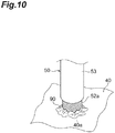
- the part 52a of the electromagnetic shield layer 52 may be brought into contact with the part 40a of the housing 40 by a conductive joining member 90 such as solder, and the part 52a may be fixed to the part 40a of the housing 40 by the conductive joining member 90.
- the part 52a of the electromagnetic shield layer 52 may be directly joined to the part 40a of the housing 40 by welding.
- the wiring board provided with the circuit configured to cause the flash lamp 10 to emit light is not limited to the two wiring boards 20 and 30 and may be a single wiring board or may be three or more wiring boards.
- the opening 45 may be formed in a wall portion of the housing 40 other than the second wall portion 42.
- the electromagnetic shield layer 52 may be exposed at least at the part of the housing 40 corresponding to the opening 45.
- the end portion of the electromagnetic shield layer 52 including the part 52a corresponding to the opening 45 may be exposed.
- the number of wires 51 is not limited.
- the holding member 60 and the fixing member 70 may be disposed inside the housing 40.
- the fixing member 70 may not be formed of a conductive material as long as at least the holding member 60 is formed of a conductive material.
- the side tube 11a of the sealed container 11 of the flash lamp 10 may be formed of another material (for example, glass and the like) in another shape (for example, substantially polygonal tube shape).
- the flash lamp 10 is of a head-on type that extracts light in a direction along the direction A but may also be of a side-on type that extracts light in a direction intersecting the direction A.
- the cathode 12 and the anode 13 are arranged in the direction intersecting the direction A but may also be arranged in the direction along the direction A.
- the plurality of lead pins 14 of the flash lamp 10 are directly fixed to the wiring board 20 by the conductive joining member such as solder but may also be fixed to the wiring board 20 via a socket to which the lead pins 14 are fitted.
Landscapes
- Engineering & Computer Science (AREA)
- General Engineering & Computer Science (AREA)
- Microelectronics & Electronic Packaging (AREA)
- Physics & Mathematics (AREA)
- General Physics & Mathematics (AREA)
- Arrangement Of Elements, Cooling, Sealing, Or The Like Of Lighting Devices (AREA)
- Stroboscope Apparatuses (AREA)
- Non-Portable Lighting Devices Or Systems Thereof (AREA)
- Shielding Devices Or Components To Electric Or Magnetic Fields (AREA)
Abstract
Description
- The present disclosure relates to a flash light source device.
- A flash light source device described in
Patent Literature 1 includes a flash lamp, a wiring board that is provided with a circuit configured to cause the flash lamp to emit light, and a housing that accommodates the flash lamp and the wiring board. - Patent Literature 1: Japanese Unexamined Patent Publication No.
2014-179205 - The flash light source device described in
Patent Literature 1 enables sufficient miniaturization. However, there is a demand for a further reduction in the size of an installation space and the suppression of emission of electromagnetic noise. - An object of the present disclosure is to provide a flash light source device capable of achieving both a reduction in the size of an installation space and the suppression of emission of electromagnetic noise.
- A flash light source device according to an embodiment of the present disclosure includes: a flash lamp; a wiring board that is provided with a circuit configured to cause the flash lamp to emit light; a housing that is formed of a conductive material and accommodates the flash lamp and the wiring board; and an electromagnetic shield cable that includes a wire directly connected to the wiring board, an electromagnetic shield layer that covers the wire, and an insulating protective layer that covers the electromagnetic shield layer, and extends to the inside and outside of the housing through an opening formed in the housing, in which the electromagnetic shield layer is exposed at least at a part corresponding to the opening, and the part corresponding to the opening in the electromagnetic shield layer is electrically connected to a part defining the opening in the housing.
- In the flash light source device, the wire of the electromagnetic shield cable is directly connected to the wiring board. Therefore, for example, compared to a case where the wiring board and the electromagnetic shield cable are electrically connected to each other via a connector, the electromagnetic shield cable can be deflected from the vicinity of the outside of the opening in the housing. Therefore, the installation space of the flash light source device can be reduced in size. In addition, the part corresponding to the opening in the electromagnetic shield layer is electrically connected to the part defining the opening in the housing. Accordingly, compared to a case where the electromagnetic shield layer at the part defining the opening in the housing is covered with the insulating protective layer and the part is not electrically connected to the electromagnetic shield layer, the amount of electromagnetic noise emitted from the wiring board and the like to the outside of the housing can be reduced. As described above, with the flash light source device, both a reduction in the size of the installation space and the suppression of emission of electromagnetic noise can be achieved.
- The flash light source device according to the embodiment of the present disclosure may further include: a holding member that is formed of a conductive material and holds the part corresponding to the opening in the electromagnetic shield layer; and a fixing member that fixes the holding member to the part defining the opening in the housing. Accordingly, with a simple configuration, the electromagnetic shield layer and the housing can be reliably, electrically connected to each other.
- In the flash light source device according to the embodiment of the present disclosure, the fixing member may be formed of a conductive material. Accordingly, with a simple configuration, the electromagnetic shield layer and the housing can be more reliably, electrically connected to each other.
- In the flash light source device according to the embodiment of the present disclosure, in a case where the fixing member is viewed in a direction in which the opening is open, the fixing member may overlap a gap formed between the part defining the opening in the housing and the part corresponding to the opening in the electromagnetic shield layer. Accordingly, the amount of electromagnetic noise emitted from the wiring board and the like to the outside of the housing through the gap can be reduced. Therefore, the emission of electromagnetic noise can be more reliably suppressed.
- In the flash light source device according to the embodiment of the present disclosure, the holding member and the fixing member may be disposed outside the housing. Accordingly, the holding member that holds the electromagnetic shield layer can be easily fixed to the part defining the opening in the housing.
- In the flash light source device according to the embodiment of the present disclosure, the electromagnetic shield layer may be exposed along the part defining the opening in the housing. Accordingly, since the part of the electromagnetic shield layer that is disposed inside the housing is covered with the insulating protective layer, it is possible to prevent a situation in which the electromagnetic shield layer comes into contact with a certain member and causes a short circuit inside the housing.
- In the flash light source device according to the embodiment of the present disclosure, a through-hole in which a sealed container of the flash lamp is disposed may be formed in the housing, the through-hole may be formed in a first wall portion of the housing, and the opening may be formed in a second wall portion of the housing that faces the first wall portion. Accordingly, the installation space of the flash light source device can be reduced in size in a direction perpendicular to a direction in which the first wall portion and the second wall portion face each other.
- According to the present disclosure, it is possible to provide a flash light source device capable of achieving both a reduction in the size of an installation space and the suppression of emission of electromagnetic noise.
-
-
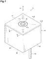
FIG. 1 is a perspective view of a flash light source device of an embodiment. -
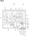
FIG. 2 is a sectional view of the flash light source device taken along line II-II ofFIG. 1 . -
FIG 3 is a sectional view of the flash light source device taken along line III-III ofFIG. 1 . -
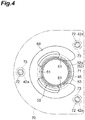
FIG. 4 is a plan view of a holding and fixing mechanism of the flash light source device ofFIG. 1 . -
FIG. 5(a) is a plan view of a first modification example of the holding and fixing mechanism.FIG. 5(b) is a plan view of a second modification example of the holding and fixing mechanism. -
FIG. 6(a) is a perspective view of a third modification example of the holding and fixing mechanism.FIG. 6(b) is a perspective view of a fourth modification example of the holding and fixing mechanism. -
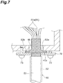
FIG. 7 is a sectional view of a fifth modification example of the holding and fixing mechanism. -
FIG. 8(a) is a side view of a sixth modification example of the holding and fixing mechanism.FIG. 8(b) is a side view of a seventh modification example of the holding and fixing mechanism. -
FIG. 9 is a plan view of an eighth modification example of the holding and fixing mechanism. -
FIG. 10 is a perspective view of a ninth modification example of the holding and fixing mechanism. - Hereinafter, an embodiment of the present disclosure will be described in detail with reference to the drawings. In each of the drawings, like elements that are the same or similar are denoted by like reference numbers, and overlapping descriptions will be omitted.
- As illustrated in
FIGS. 1 ,2 , and3 , a flashlight source device 1 includes aflash lamp 10, twowiring boards housing 40. Theflash lamp 10 includes a sealedcontainer 11, acathode 12, ananode 13, a trigger electrode (not illustrated), a sparker electrode (not illustrated), and a plurality oflead pins 14. Theflash lamp 10 has a configuration in which the plurality oflead pins 14 protrude from one end portion of the sealedcontainer 11. Unlike a straight tube type flash lamp (one having a configuration in which a cathode and an anode are disposed apart from each other at both ends of a straight tube), theflash lamp 10 having such a configuration is appropriate for lighting at a high frequency of, for example, 10 Hz or higher. - Discharge gas (for example, xenon gas) is sealed in the sealed
container 11. The sealedcontainer 11 is constituted by aside tube 11a, astem 11b, and a light-transmittingmember 11c. Theside tube 11a is formed of a metal material, for example, in a cylindrical shape. The center line of theside tube 11a is parallel to a direction A. Thestem 11b is formed of a metal material, for example, in a disk shape. Thestem 11b blocks one end portion of theside tube 11a. The light-transmittingmember 11c is formed of glass, for example, in a disk shape. The light-transmittingmember 11c blocks the other end portion of theside tube 11a. Asealing tube 15 is provided in thestem 11b. Thesealing tube 15 protrudes from one end portion of the sealedcontainer 11. Thesealing tube 15 is used to fill the sealedcontainer 11 with discharge gas, and is sealed after the filling with the discharge gas. - The
cathode 12 and theanode 13 face each other in a direction intersecting the direction A (here, a direction perpendicular to the direction A). Thecathode 12 and theanode 13 cause an arc discharge in the sealedcontainer 11. The trigger electrode causes a preliminary discharge prior to the arc discharge. The sparker electrode enables stable generation of the arc discharge. Light generated by the arc discharge is emitted along the direction A via the light-transmittingmember 11c. Thecathode 12, theanode 13, the trigger electrode, and the sparker electrode are respectively fixed to the end portions of the lead pins 14. Each of the lead pins 14 penetrates through thestem 11b via an insulating member (not illustrated) and protrudes from one end portion of the sealedcontainer 11 as described above. - The
wiring board 20 has afront surface 20a and arear surface 20b that oppose each other in the direction A. Thewiring board 20 is disposed in thehousing 40 in a state in which thefront surface 20a faces afirst wall portion 41 side of thehousing 40. Thewiring board 20 is fixed to thefirst wall portion 41 of thehousing 40 with aspacer 2 interposed therebetween. Each of the lead pins 14 of theflash lamp 10 is fixed to thefront surface 20a of thewiring board 20 by a conductive joining member such as solder. Accordingly, theflash lamp 10 is electrically connected to a circuit provided in the wiring board 20 (a circuit configured to cause theflash lamp 10 to emit light). - On the
front surface 20a and therear surface 20b of thewiring board 20, circuit components such as a plurality ofchip capacitors 21a and a plurality ofresistance elements 22 are mounted. The circuit components constitute the circuit configured to cause theflash lamp 10 to emit light. As an example, the plurality ofchip capacitors 21a constitute apower supply unit 21 for charging and discharging current to be supplied to theflash lamp 10. In thepower supply unit 21, the plurality ofchip capacitors 21a are connected in parallel. In addition, a through-hole 20c is formed in thewiring board 20. In the through-hole 20c, the sealingtube 15 of theflash lamp 10 is disposed. - A
wiring board 30 has afront surface 30a and arear surface 30b that oppose each other in the direction A. Thewiring board 30 is disposed in thehousing 40 in a state in which thefront surface 30a faces thewiring board 20 side. Thewiring board 30 is fixed to thewiring board 20 with aspacer 3 interposed therebetween. On thefront surface 30a and therear surface 30b of thewiring board 30, circuit components such as anelectrolytic capacitor 31, a transformer (boosting unit) 32, and aresistance element 33 are mounted. The circuit components constitute the circuit configured to cause theflash lamp 10 to emit light. As an example, theelectrolytic capacitor 31 removes electromagnetic noise. Thetransformer 32 is provided between the primary circuit on the power source side and the secondary circuit on theflash lamp 10 side. Thetransformer 32 amplifies (boosts) a pulse voltage of, for example, 100 to 300 V input to the primary side coil, and outputs a pulse voltage of, for example, 5 to 7 kV from the secondary side coil. - The
housing 40 includes, in addition to thefirst wall portion 41 described above, asecond wall portion 42 and a plurality ofthird wall portions 43. Thefirst wall portion 41 and thesecond wall portion 42 face each other in the direction A with the twowiring boards third wall portions 43 stand upright on the peripheral edge portion of thesecond wall portion 42. Thesecond wall portion 42 and the plurality ofthird wall portions 43 constitute a container with a bottom, which is integrally formed. In a state of being fitted to an opening of the container with a bottom, thefirst wall portion 41 is fixed to the opening, for example, by screwing. - A through-
hole 41a is formed in thefirst wall portion 41. The sealedcontainer 11 of theflash lamp 10 is disposed in the through-hole 41a. The outer surface of the light-transmittingmember 11c of theflash lamp 10 is flush with the outer surface of thefirst wall portion 41. Theside tube 11a of the sealedcontainer 11 and thefirst wall portion 41 are into contact with each other to be thermally connected to each other. Accordingly, heat can be efficiently released from theflash lamp 10 that generates heat due to light emission to the first wall portion 41 (furthermore, the first wall portion 41). In addition, theside tube 11a of the sealedcontainer 11 and thefirst wall portion 41 may be thermally joined to each other by disposing a heat transfer member therebetween. - The housing 40 (that is, the
first wall portion 41, thesecond wall portion 42, and the plurality of third wall portions 43) are formed of a conductive material such as a metal material, for example, in a rectangular parallelepiped shape. Thehousing 40 accommodates theflash lamp 10 and the twowiring boards housing 40 accommodates theflash lamp 10" means that thehousing 40 accommodates a part of each of the lead pins 14 protruding from one end portion of the sealedcontainer 11. - Furthermore, the flash
light source device 1 includes anelectromagnetic shield cable 50, a holdingmember 60, and a fixingmember 70. Theelectromagnetic shield cable 50 includes a plurality ofwires 51, anelectromagnetic shield layer 52, and an insulatingprotective layer 53. Theelectromagnetic shield cable 50 is a flexible cable for electrically connecting the twowiring boards electromagnetic shield cable 50 extends to the inside and the outside of thehousing 40 through anopening 45 formed in thesecond wall portion 42 of thehousing 40, for example, in a circular shape. - The plurality of
wires 51 are exposed to the inside of thehousing 40. That is, theelectromagnetic shield layer 52 and the insulatingprotective layer 53 are partially removed from the end portion of theelectromagnetic shield cable 50 such thatend portions 51a of the plurality ofwires 51 are exposed to the outside (the space in the housing 40). Each of thewires 51 is directly connected to a predetermined portion of therear surface 30b of thewiring board 30. As an example, an insulating protective film is partially removed from theend portion 51a of each of thewires 51 such that the end portion of the conducting wire is exposed and the conducting wire is fixed to a predetermined portion of therear surface 30b of thewiring board 30 by a conductive joining member such as solder. As described above, each of thewires 51 is directly connected to thewiring board 30 without a connecting component such as a connector interposed therebetween. In addition, each of thewires 51 is, for example, a power supply wire or a signal input wire. - The
electromagnetic shield layer 52 covers the plurality ofwires 51 over substantially the entire length of theelectromagnetic shield cable 50. Theelectromagnetic shield layer 52 is formed of a conductive material such as a metal material in a tubular shape. As an example, theelectromagnetic shield layer 52 is formed in a tubular shape by a plurality of metal wires braided in a mesh shape, and the metal wires are electrically connected to each other. The insulatingprotective layer 53 covers theelectromagnetic shield layer 52 over substantially the entire length of theelectromagnetic shield cable 50. The insulatingprotective layer 53 is formed of an insulating material such as elastomer in a tubular shape. - The
electromagnetic shield layer 52 is exposed at apart 52a corresponding to theopening 45. That is, the insulatingprotective layer 53 is partially removed from thepart 52a corresponding to theopening 45 in theelectromagnetic shield layer 52 such that thepart 52a of theelectromagnetic shield layer 52 is exposed to the outside. More specifically, theelectromagnetic shield layer 52 is exposed along apart 40a defining theopening 45 in the housing 40 (a part including at least one of a region of the outer surface of thehousing 40 along the edge of theopening 45, the inner surface of theopening 45, and a region of the inner surface of thehousing 40 along the edge of the opening 45). That is, the insulatingprotective layer 53 is removed annularly along thepart 40a defining theopening 45 in thehousing 40, so that thepart 52a of theelectromagnetic shield layer 52 is exposed to the outside. - As illustrated in
FIG. 4 , the holdingmember 60 is formed of a conductive material such as a metal material in an annular shape (C-shape) that is partially cut out. The holdingmember 60 is provided with a plurality ofclaw portions 61 protruding inward. The holdingmember 60 comes into contact with thepart 52a of theelectromagnetic shield layer 52 with the plurality ofclaw portions 61 by the elastic deformation force and holds thepart 52a. As illustrated inFIGS. 2 and3 , the holdingmember 60 is into contact with thepart 40a of thehousing 40 on the outside of thehousing 40. Accordingly, thepart 52a of theelectromagnetic shield layer 52 is reliably, electrically connected to thepart 40a of thehousing 40 via the holdingmember 60. - As illustrated in
FIG 4 , the fixingmember 70 is formed of a conductive material such as a metal material in a plate shape. In the fixingmember 70, anopening 71 and a plurality of through-holes 72 are formed. Theelectromagnetic shield cable 50 is inserted through theopening 71. The plurality of through-holes 72 respectively correspond to a plurality of threadedholes 42a formed in thesecond wall portion 42 of thehousing 40. Ascrew 73 formed of a conductive material such as a metal material is screwed into each of the threadedholes 42a through the corresponding through-hole 72. In addition, inFIG 4 , the fixingmember 70 and thescrews 73 are indicated by two-dot chain lines, and thewires 51 are omitted. As illustrated inFIGS. 2 and3 , the fixingmember 70 causes the holdingmember 60 to be interposed between the fixingmember 70 and thehousing 40 on the outside of thehousing 40 so as to cover the holdingmember 60 such that the holdingmember 60 is reliably brought into contact with and fixed to thepart 40a of thehousing 40. - As illustrated in
FIG. 4 , the inner diameter of theopening 45 of thehousing 40 is larger than the outer diameter of theelectromagnetic shield cable 50. The inner diameter of theopening 71 of the fixingmember 70 is larger than the outer diameter of theelectromagnetic shield cable 50 and is smaller than the inner diameter of theopening 45 of thehousing 40. Therefore, in a case where the fixingmember 70 is viewed in a direction in which theopening 45 is open (a direction parallel to the center line of theopening 45 having a circular shape), to cover the gap formed between thepart 40a of thehousing 40 and thepart 52a of theelectromagnetic shield layer 52, the fixingmember 70 overlaps the gap. - The operation of the flash
light source device 1 configured as described above will be described. First, power is supplied to the main power source unit provided in thewiring board 30 via theelectromagnetic shield cable 50 such that thepower supply unit 21 is charged. Thereafter, a voltage is applied between thecathode 12 and theanode 13. On the other hand, a pulse voltage of, for example, 100 to 300 V, is applied to the primary side coil of thetransformer 32. The pulse voltage applied to the primary side coil is amplified (boosted) in thetransformer 32, and a pulse voltage of, for example, 5 to 7 kV is output from the secondary side coil. The pulse voltage output from the secondary side coil is applied to theanode 13 and the sparker electrode. - In the
flash lamp 10, first, a preliminary discharge occurs due to the sparker electrode, and subsequently, a preliminary discharge occurs between thecathode 12 or theanode 13 and the trigger electrode, whereby a preliminary discharge path is formed. Immediately thereafter, a main discharge occurs along the preliminary discharge path between thecathode 12 and theanode 13. When the main discharge (arc discharge) occurs between thecathode 12 and theanode 13, a current is supplied through the main power source unit provided on thewiring board 30 and accumulated charge is output from thepower supply unit 21. Light generated by the arc discharge is emitted along the direction A via the light-transmittingmember 11c. - As described above, in the flash
light source device 1, thewires 51 of theelectromagnetic shield cable 50 are directly connected to thewiring board 30. Therefore, for example, compared to a case where thewiring board 30 and theelectromagnetic shield cable 50 are electrically connected to each other via a connector, theelectromagnetic shield cable 50 can be deflected from the vicinity of the outside of theopening 45 in thehousing 40. Therefore, the installation space of the flashlight source device 1 can be reduced in size. In addition, thepart 52a corresponding to theopening 45 in theelectromagnetic shield layer 52 is electrically connected to thepart 40a defining theopening 45 in thehousing 40. Accordingly, compared to a case where theelectromagnetic shield layer 52 at thepart 40a defining theopening 45 in thehousing 40 is covered with the insulatingprotective layer 53 and thepart 40a is not electrically connected to theelectromagnetic shield layer 52, the amount of electromagnetic noise emitted from each of thewiring boards housing 40 can be reduced. As described above, with the flashlight source device 1, both a reduction in the size of the installation space and the suppression of emission of electromagnetic noise can be achieved. - In addition, in the flash light source device I, the
transformer 32 that amplifies (boosts) a pulse voltage is provided on thewiring board 30, and the pulse voltage amplified (boosted) by thetransformer 32 is input to each of the lead pins 14 of theflash lamp 10. Therefore, in particular, in the flashlight source device 1, it is extremely important to accommodate theflash lamp 10 and thewiring boards housing 40 and to reduce the amount of electromagnetic noise emitted from each of thewiring boards housing 40 by the configuration as described above. - In addition, the flash
light source device 1, thepart 52a of theelectromagnetic shield layer 52 is held by the holdingmember 60 formed of a conductive material, and the holdingmember 60 is fixed to thepart 40a of thehousing 40 by the fixingmember 70. Accordingly, with a simple configuration, theelectromagnetic shield layer 52 and thehousing 40 can be reliably, electrically connected to each other. - In addition, in the flash
light source device 1, the fixingmember 70 is formed of a conductive material. Accordingly, with a simple configuration, theelectromagnetic shield layer 52 and thehousing 40 can be more reliably, electrically connected to each other. - In addition, in the flash
light source device 1, in a case where the fixingmember 70 is viewed in the direction in which theopening 45 is open, the fixingmember 70 overlaps the gap formed between thepart 40a of thehousing 40 and thepart 52a of theelectromagnetic shield layer 52. Accordingly, since the gap is covered with the fixingmember 70, the amount of electromagnetic noise emitted from thewiring boards housing 40 through the gap can be reduced. Therefore, the emission of electromagnetic noise can be more reliably suppressed. In addition, the inner diameter of theopening 45 of thehousing 40 and the inner diameter of theopening 71 of the fixingmember 70 are larger than the outer diameter of theelectromagnetic shield cable 50 to enable theelectromagnetic shield cable 50 to be easily inserted. - In addition, in the flash
light source device 1, the holdingmember 60 and the fixingmember 70 are disposed outside thehousing 40. Accordingly, the holdingmember 60 that holds theelectromagnetic shield layer 52 can be easily fixed to thepart 40a of thehousing 40. - In addition, in the flash
light source device 1, theelectromagnetic shield layer 52 is exposed along thepart 40a of thehousing 40. Accordingly, since the part of theelectromagnetic shield layer 52 that is disposed inside thehousing 40 is covered with the insulatingprotective layer 53, it is possible to prevent a situation in which theelectromagnetic shield layer 52 comes into contact with a certain member and causes a short circuit inside thehousing 40. Furthermore, even when theelectromagnetic shield cable 50 is pulled against the holding force of theelectromagnetic shield cable 50 by the holdingmember 60, the insulatingprotective layer 53 that covers the part of theelectromagnetic shield layer 52 that is disposed inside thehousing 40 comes into contact with the holdingmember 60, so that a physical load is prevented from being applied to the connection portion between thewiring board 30 and each of thewires 51. - In addition, in the flash
light source device 1, the through-hole 41a in which the sealedcontainer 11 of theflash lamp 10 is disposed is formed in thefirst wall portion 41 of thehousing 40, and theopening 45 through which theelectromagnetic shield cable 50 is inserted is formed in thesecond wall portion 42 of thehousing 40 that faces thefirst wall portion 41. Accordingly, in particular, the installation space of the flashlight source device 1 can be reduced in size in the direction perpendicular to the direction in which thefirst wall portion 41 and thesecond wall portion 42 face each other (that is, the direction A). - While the embodiment of the present disclosure has been described above, the flash light source device of the present disclosure is not limited to the above-described embodiment For example, as illustrated in
FIGS. 5(a) and 5(b) , instead of the holdingmember 60 described above, a holdingmember 60 that holds thepart 52a of theelectromagnetic shield layer 52 by plastic deformation may be used. The holdingmember 60 illustrated inFIG. 5(a) is formed of a conductive material such as a metal material in an annular shape (C-shape) that is partially cut out In this case, the holdingmember 60 is deformed so that both end portions of the holdingmember 60 that face each other at the cut-out part overlap each other, thepart 52a of theelectromagnetic shield layer 52 comes into contact with the holdingmember 60, and thepart 52a is held by the holdingmember 60. The holdingmember 60 illustrated inFIG. 5(b) is formed of a conductive material such as a metal material in an annular shape. In this case, the parts of the holdingmember 60, the parts that face each other with thepart 52a of theelectromagnetic shield layer 52 interposed therebetween, are deformed so as to protrude inward into a convex shape such that thepart 52a of theelectromagnetic shield layer 52 comes into contact with the holdingmember 60, and thepart 52a is held by the holdingmember 60. In any case ofFIGS. 5(a) and 5(b) , the holdingmember 60 can be fixed to thepart 40a of thehousing 40 using the fixingmember 70 described above. - In addition, as illustrated in
FIGS. 6(a) and 6(b) , instead of the holdingmember 60 and the fixingmember 70 described above, a holdingmember 80 having both a holding function and a fixing function may be used. The holdingmember 80 illustrated inFIG. 6(a) includes acircular tube part 81, aflange part 82, and a pair ofbase parts 83. A slit 81 a is formed in thecircular tube part 81. The pair ofbase parts 83 are provided in thecircular tube part 81 so as to face each other with theslit 81a interposed therebetween. Theflange part 82 is provided at one end portion of thecircular tube part 81. Aslit 82a is formed in theflange part 82 so as to be continuous with theslit 81a. Thecircular tube part 81, theflange part 82, and the pair ofbase parts 83 are integrally formed of a conductive material such as a metal material. In this case, in a state in which thepart 52a of theelectromagnetic shield layer 52 is inserted through thecircular tube part 81, the distance between the pair ofbase parts 83 is narrowed by a screw, so that thepart 52a of theelectromagnetic shield layer 52 comes into contact with thecircular tube part 81 and thepart 52a is held by thecircular tube part 81. In addition, theflange part 82 is fixed to thepart 40a of thehousing 40 by a screw. The holdingmember 80 illustrated inFIG. 6(b) is a U-shaped member in which agroove 80a into which theelectromagnetic shield cable 50 is introduced is formed in a flat plate-shaped member, and in the U-shaped member, a plurality ofclaw portions 84 that protrude to narrow thegroove 80a are provided. The holdingmember 80 is configured to be fixed to thepart 40a of thehousing 40 by a screw. In this case, thepart 52a of theelectromagnetic shield layer 52 comes into contact with each of theclaw portions 84 of the holdingmember 80, and thepart 52a is held by the plurality ofclaw portions 84. - In addition, the
part 52a of theelectromagnetic shield layer 52 may be brought into direct contact with thepart 40a of thehousing 40. In an example illustrated inFIG 7 , the end portion of theelectromagnetic shield layer 52 including thepart 52a corresponding to theopening 45 is exposed, and the exposed end portion of the electromagnetic shield layer 25 is deformed in a disk shape having a diameter larger than theopening 45, so that the aflange portion 52b is formed in thepart 52a of theelectromagnetic shield layer 52. In addition, theflange portion 52b is fixed to thepart 40a of thehousing 40 by the fixingmember 70 such that thepart 52a of theelectromagnetic shield layer 52 is brought into direct contact with thepart 40a of thehousing 40. - In addition, as illustrated in
FIGS. 8(a) and 8(b) , instead of the holdingmember 60 and the fixingmember 70, a holdingmember 80 having both a holding function and a fixing function may be used. The holdingmember 80 illustrated inFIG. 8(a) includes a pair ofannular parts 85 and a plurality ofsupport parts 86. The plurality ofsupport parts 86 are stretched between the pair ofannular parts 85 so that the space of the center portion becomes narrow. The pair ofannular parts 85 and the plurality ofsupport parts 86 are integrally formed of a conductive material such as a metal material. In this case, in a state in which the plurality ofsupport parts 86 are disposed in theopening 45 of thehousing 40, thepart 52a of theelectromagnetic shield layer 52 is inserted through the holdingmember 80 such that the plurality ofsupport parts 86 are deformed to widen the space of the center portion and come into contact with thepart 52a of theelectromagnetic shield layer 52. Accordingly, thepart 52a of theelectromagnetic shield layer 52 is held by the plurality ofsupport parts 86 and thepart 52a of theelectromagnetic shield layer 52 is electrically connected and fixed to thepart 40a of thehousing 40. A holdingmember 80 illustrated inFIG. 8(b) includes a pair ofannular parts 85, a plurality ofsupport parts 87, and a plurality ofclaw parts 88. The plurality ofsupport parts 87 are stretched between the pair ofannular parts 85. The plurality ofclaw parts 88 extend from one pair ofannular parts 85 so that the space of the center portion becomes narrow. The pair ofannular parts 85, the plurality ofsupport parts 87, and the plurality ofclaw parts 88 are integrally formed of a conductive material such as a metal material. In this case, in a state in which the plurality ofsupport parts 87 are fixed in theopening 45 of thehousing 40, thepart 52a of theelectromagnetic shield layer 52 is inserted through the holdingmember 80 such that the plurality ofclaw parts 88 are deformed to widen the space of the center portion and come into contact with thepart 52a of theelectromagnetic shield layer 52. Accordingly, thepart 52a of theelectromagnetic shield layer 52 is held by the plurality ofclaw parts 88 and thepart 52a of theelectromagnetic shield layer 52 is electrically connected and fixed to thepart 40a of thehousing 40. - In addition, as illustrated in
FIG. 9 , thepart 40a defining theopening 45 in thehousing 40 may be constituted by a plurality of movable parts having arc shaped grooves so that the size of theopening 45 is variable. In this case, one of the parts constituting thepart 40a of thehousing 40 is shifted relative to the other part in a direction perpendicular toFIG. 9 (a direction intersecting the direction in which theopening 45 is open) to achieve an overlapping positional relationship, so that the size (width) of theopening 45 is narrowed and thepart 52a of theelectromagnetic shield layer 52 can be interposed therebetween. Accordingly, thepart 52a of theelectromagnetic shield layer 52 is electrically connected and fixed to thepart 40a of thehousing 40. In addition, as illustrated inFIG 10 , thepart 52a of theelectromagnetic shield layer 52 may be brought into contact with thepart 40a of thehousing 40 by a conductive joiningmember 90 such as solder, and thepart 52a may be fixed to thepart 40a of thehousing 40 by the conductive joiningmember 90. Alternatively, thepart 52a of theelectromagnetic shield layer 52 may be directly joined to thepart 40a of thehousing 40 by welding. - Furthermore, the wiring board provided with the circuit configured to cause the
flash lamp 10 to emit light is not limited to the twowiring boards opening 45 may be formed in a wall portion of thehousing 40 other than thesecond wall portion 42. - In addition, in the
electromagnetic shield cable 50, theelectromagnetic shield layer 52 may be exposed at least at the part of thehousing 40 corresponding to theopening 45. As an example, as illustrated inFIG 7 , the end portion of theelectromagnetic shield layer 52 including thepart 52a corresponding to theopening 45 may be exposed. In addition, the number ofwires 51 is not limited. - In addition, the holding
member 60 and the fixingmember 70 may be disposed inside thehousing 40. In addition, the fixingmember 70 may not be formed of a conductive material as long as at least the holdingmember 60 is formed of a conductive material. - In addition, the
side tube 11a of the sealedcontainer 11 of theflash lamp 10 may be formed of another material (for example, glass and the like) in another shape (for example, substantially polygonal tube shape). In addition, theflash lamp 10 is of a head-on type that extracts light in a direction along the direction A but may also be of a side-on type that extracts light in a direction intersecting the direction A. In addition, thecathode 12 and theanode 13 are arranged in the direction intersecting the direction A but may also be arranged in the direction along the direction A. In addition, the plurality of lead pins 14 of theflash lamp 10 are directly fixed to thewiring board 20 by the conductive joining member such as solder but may also be fixed to thewiring board 20 via a socket to which the lead pins 14 are fitted. - 1: flash light source device, 10: flash lamp, 11: sealed container, 20, 30: wiring board, 40: housing, 40a: part, 41: first wall portion, 41a: through-hole, 42: second wall portion, 45: opening, 50: electromagnetic shield cable, 51: wire, 52: electromagnetic shield layer, 52a: part, 53: insulating protective layer, 60: holding member, 70: fixing member.
Claims (7)
- A flash light source device comprising:a flash lamp;a wiring board that is provided with a circuit configured to cause the flash lamp to emit light;a housing that is formed of a conductive material and accommodates the flash lamp and the wiring board; andan electromagnetic shield cable that includes a wire directly connected to the wiring board, an electromagnetic shield layer that covers the wire, and an insulating protective layer that covers the electromagnetic shield layer, and extends to the inside and outside of the housing through an opening formed in the housing,wherein the electromagnetic shield layer is exposed at least at a part corresponding to the opening, andthe part corresponding to the opening in the electromagnetic shield layer is electrically connected to a part defining the opening in the housing.
- The flash light source device according to claim 1, further comprising:a holding member that is formed of a conductive material and holds the part corresponding to the opening in the electromagnetic shield layer; anda fixing member that fixes the holding member to the part defining the opening in the housing.
- The flash light source device according to claim 2,
wherein the fixing member is formed of a conductive material. - The flash light source device according to claim 3,
wherein, in a case where the fixing member is viewed in a direction in which the opening is open, the fixing member overlaps a gap formed between the part defining the opening in the housing and the part corresponding to the opening in the electromagnetic shield layer. - The flash light source device according to any one of claims 2 to 4,
wherein the holding member and the fixing member are disposed outside the housing. - The flash light source device according to any one of claims 1 to 5,
wherein the electromagnetic shield layer is exposed along the part defining the opening in the housing. - The flash light source device according to any one of claims 1 to 6,
wherein a through-hole in which a sealed container of the flash lamp is disposed is formed in the housing,
the through-hole is formed in a first wall portion of the housing, and
the opening is formed in a second wall portion of the housing that faces the first wall portion.
Applications Claiming Priority (2)
| Application Number | Priority Date | Filing Date | Title |
|---|---|---|---|
| JP2016046650A JP6783531B2 (en) | 2016-03-10 | 2016-03-10 | Flash light source device |
| PCT/JP2017/002746 WO2017154394A1 (en) | 2016-03-10 | 2017-01-26 | Flash light source device |
Publications (2)
| Publication Number | Publication Date |
|---|---|
| EP3428525A1 true EP3428525A1 (en) | 2019-01-16 |
| EP3428525A4 EP3428525A4 (en) | 2019-11-27 |
Family
ID=59789089
Family Applications (1)
| Application Number | Title | Priority Date | Filing Date |
|---|---|---|---|
| EP17762740.3A Withdrawn EP3428525A4 (en) | 2016-03-10 | 2017-01-26 | LIGHT BEAM SOURCE DEVICE |
Country Status (5)
| Country | Link |
|---|---|
| US (1) | US10514142B2 (en) |
| EP (1) | EP3428525A4 (en) |
| JP (1) | JP6783531B2 (en) |
| CN (1) | CN108779911A (en) |
| WO (1) | WO2017154394A1 (en) |
Families Citing this family (4)
| Publication number | Priority date | Publication date | Assignee | Title |
|---|---|---|---|---|
| CN110011082A (en) * | 2019-04-15 | 2019-07-12 | 苏州浪潮智能科技有限公司 | A kind of server and its cable earthing or grounding means |
| CN114102270B (en) * | 2021-11-10 | 2022-09-23 | 西北核技术研究所 | Method for improving radiation light intensity of metal wire in strong pulse flash light source |
| JP2026017657A (en) * | 2024-07-24 | 2026-02-05 | 浜松ホトニクス株式会社 | Electron Tube Unit |
| JP2026067282A (en) * | 2024-10-08 | 2026-04-20 | 浜松ホトニクス株式会社 | flash lamp |
Family Cites Families (8)
| Publication number | Priority date | Publication date | Assignee | Title |
|---|---|---|---|---|
| JPS6259974U (en) * | 1985-10-04 | 1987-04-14 | ||
| US5313373A (en) * | 1992-11-25 | 1994-05-17 | United Parcel Service Of America, Inc. | Apparatus for the uniform illumination of a surface |
| JPH07336085A (en) * | 1994-06-03 | 1995-12-22 | Sumitomo Electric Ind Ltd | Penetration part of cable with metal shield layer |
| JP3788813B2 (en) | 1995-07-13 | 2006-06-21 | 浜松ホトニクス株式会社 | Light source device |
| JPH09102692A (en) * | 1995-10-05 | 1997-04-15 | Toshiba Corp | Shield box |
| IT1277694B1 (en) * | 1995-12-22 | 1997-11-11 | Italtel Spa | DEVICE FOR SHIELDING AGAINST ELECTROMAGNETIC DISTURBANCE OF A SINGLE CABLE |
| JP2014170921A (en) * | 2013-02-08 | 2014-09-18 | Ushio Inc | Ultraviolet irradiation device |
| JP6178087B2 (en) * | 2013-03-14 | 2017-08-09 | 浜松ホトニクス株式会社 | Flash light source device |
-
2016
- 2016-03-10 JP JP2016046650A patent/JP6783531B2/en active Active
-
2017
- 2017-01-26 US US16/081,627 patent/US10514142B2/en active Active
- 2017-01-26 EP EP17762740.3A patent/EP3428525A4/en not_active Withdrawn
- 2017-01-26 CN CN201780015991.2A patent/CN108779911A/en active Pending
- 2017-01-26 WO PCT/JP2017/002746 patent/WO2017154394A1/en not_active Ceased
Also Published As
| Publication number | Publication date |
|---|---|
| US20190086048A1 (en) | 2019-03-21 |
| JP2017162704A (en) | 2017-09-14 |
| WO2017154394A1 (en) | 2017-09-14 |
| JP6783531B2 (en) | 2020-11-11 |
| EP3428525A4 (en) | 2019-11-27 |
| US10514142B2 (en) | 2019-12-24 |
| CN108779911A (en) | 2018-11-09 |
Similar Documents
| Publication | Publication Date | Title |
|---|---|---|
| US10514142B2 (en) | Flash light source device | |
| US20090225560A1 (en) | Aircraft External Illumination Lamp | |
| US9704702B2 (en) | Flash light source device | |
| US20080191627A1 (en) | High-Voltage Pulse Generator, And Lighting Apparatus And Vehicle Having The Same | |
| KR101067195B1 (en) | Flash unit, manufacturing method of flash unit and digital camera | |
| US8994268B2 (en) | Strobe device | |
| US4156890A (en) | Flash assembly using elongated trigger bar | |
| KR100912334B1 (en) | Gas discharge tube | |
| US7573201B2 (en) | Dielectric barrier discharge lamp having pluggable electrodes | |
| US20060066191A1 (en) | Dielectric barrier discharge lamp having an electric shield | |
| US8922120B2 (en) | Strobe device | |
| US20140185298A1 (en) | Strobe device | |
| JP2014032812A (en) | Lighting device | |
| US20120098427A1 (en) | Discharge lamp lighting apparatus and manufacturing method thereof | |
| JP2011221080A (en) | Strobe device and imaging apparatus | |
| JP4636966B2 (en) | Low speed electronic measuring device | |
| KR100510989B1 (en) | Flash apparatus with xenon tube | |
| JP6502108B2 (en) | Power supply for light source with built-in igniter | |
| JP2002148689A (en) | Stroboscopic device | |
| KR20140101312A (en) | Ultraviolet irradiation apparatus | |
| US20130343047A1 (en) | Strobe device | |
| JP2012038471A (en) | Discharge lamp lighting device | |
| CN112447384A (en) | Boosting device | |
| CN102385218A (en) | Flashing device | |
| JP2003248259A (en) | Flash light emitting device |
Legal Events
| Date | Code | Title | Description |
|---|---|---|---|
| STAA | Information on the status of an ep patent application or granted ep patent |
Free format text: STATUS: THE INTERNATIONAL PUBLICATION HAS BEEN MADE |
|
| PUAI | Public reference made under article 153(3) epc to a published international application that has entered the european phase |
Free format text: ORIGINAL CODE: 0009012 |
|
| STAA | Information on the status of an ep patent application or granted ep patent |
Free format text: STATUS: REQUEST FOR EXAMINATION WAS MADE |
|
| 17P | Request for examination filed |
Effective date: 20181010 |
|
| AK | Designated contracting states |
Kind code of ref document: A1 Designated state(s): AL AT BE BG CH CY CZ DE DK EE ES FI FR GB GR HR HU IE IS IT LI LT LU LV MC MK MT NL NO PL PT RO RS SE SI SK SM TR |
|
| AX | Request for extension of the european patent |
Extension state: BA ME |
|
| DAV | Request for validation of the european patent (deleted) | ||
| DAX | Request for extension of the european patent (deleted) | ||
| A4 | Supplementary search report drawn up and despatched |
Effective date: 20191023 |
|
| RIC1 | Information provided on ipc code assigned before grant |
Ipc: H05K 9/00 20060101AFI20191018BHEP Ipc: F21V 25/00 20060101ALI20191018BHEP Ipc: H01J 61/90 20060101ALI20191018BHEP |
|
| STAA | Information on the status of an ep patent application or granted ep patent |
Free format text: STATUS: EXAMINATION IS IN PROGRESS |
|
| 17Q | First examination report despatched |
Effective date: 20200729 |
|
| STAA | Information on the status of an ep patent application or granted ep patent |
Free format text: STATUS: THE APPLICATION IS DEEMED TO BE WITHDRAWN |
|
| 18D | Application deemed to be withdrawn |
Effective date: 20210819 |