EP3427003B1 - Compact interferometer, related bio-chemical sensor and measurement device - Google Patents
Compact interferometer, related bio-chemical sensor and measurement device Download PDFInfo
- Publication number
- EP3427003B1 EP3427003B1 EP17709074.3A EP17709074A EP3427003B1 EP 3427003 B1 EP3427003 B1 EP 3427003B1 EP 17709074 A EP17709074 A EP 17709074A EP 3427003 B1 EP3427003 B1 EP 3427003B1
- Authority
- EP
- European Patent Office
- Prior art keywords
- interferometer
- layer
- signal
- measurement device
- phase
- Prior art date
- Legal status (The legal status is an assumption and is not a legal conclusion. Google has not performed a legal analysis and makes no representation as to the accuracy of the status listed.)
- Active
Links
Images



Classifications
-
- G—PHYSICS
- G01—MEASURING; TESTING
- G01B—MEASURING LENGTH, THICKNESS OR SIMILAR LINEAR DIMENSIONS; MEASURING ANGLES; MEASURING AREAS; MEASURING IRREGULARITIES OF SURFACES OR CONTOURS
- G01B9/00—Measuring instruments characterised by the use of optical techniques
- G01B9/02—Interferometers
- G01B9/02049—Interferometers characterised by particular mechanical design details
- G01B9/02051—Integrated design, e.g. on-chip or monolithic
-
- G—PHYSICS
- G01—MEASURING; TESTING
- G01B—MEASURING LENGTH, THICKNESS OR SIMILAR LINEAR DIMENSIONS; MEASURING ANGLES; MEASURING AREAS; MEASURING IRREGULARITIES OF SURFACES OR CONTOURS
- G01B9/00—Measuring instruments characterised by the use of optical techniques
- G01B9/02—Interferometers
- G01B9/02001—Interferometers characterised by controlling or generating intrinsic radiation properties
- G01B9/02002—Interferometers characterised by controlling or generating intrinsic radiation properties using two or more frequencies
- G01B9/02004—Interferometers characterised by controlling or generating intrinsic radiation properties using two or more frequencies using frequency scans
-
- G—PHYSICS
- G01—MEASURING; TESTING
- G01N—INVESTIGATING OR ANALYSING MATERIALS BY DETERMINING THEIR CHEMICAL OR PHYSICAL PROPERTIES
- G01N21/00—Investigating or analysing materials by the use of optical means, i.e. using sub-millimetre waves, infrared, visible or ultraviolet light
- G01N21/17—Systems in which incident light is modified in accordance with the properties of the material investigated
- G01N21/41—Refractivity; Phase-affecting properties, e.g. optical path length
- G01N21/45—Refractivity; Phase-affecting properties, e.g. optical path length using interferometric methods; using Schlieren methods
-
- G—PHYSICS
- G01—MEASURING; TESTING
- G01N—INVESTIGATING OR ANALYSING MATERIALS BY DETERMINING THEIR CHEMICAL OR PHYSICAL PROPERTIES
- G01N21/00—Investigating or analysing materials by the use of optical means, i.e. using sub-millimetre waves, infrared, visible or ultraviolet light
- G01N21/17—Systems in which incident light is modified in accordance with the properties of the material investigated
- G01N21/55—Specular reflectivity
- G01N21/552—Attenuated total reflection
- G01N21/553—Attenuated total reflection and using surface plasmons
-
- G—PHYSICS
- G01—MEASURING; TESTING
- G01N—INVESTIGATING OR ANALYSING MATERIALS BY DETERMINING THEIR CHEMICAL OR PHYSICAL PROPERTIES
- G01N33/00—Investigating or analysing materials by specific methods not covered by groups G01N1/00 - G01N31/00
- G01N33/48—Biological material, e.g. blood, urine; Haemocytometers
- G01N33/50—Chemical analysis of biological material, e.g. blood, urine; Testing involving biospecific ligand binding methods; Immunological testing
- G01N33/68—Chemical analysis of biological material, e.g. blood, urine; Testing involving biospecific ligand binding methods; Immunological testing involving proteins, peptides or amino acids
-
- C—CHEMISTRY; METALLURGY
- C12—BIOCHEMISTRY; BEER; SPIRITS; WINE; VINEGAR; MICROBIOLOGY; ENZYMOLOGY; MUTATION OR GENETIC ENGINEERING
- C12Q—MEASURING OR TESTING PROCESSES INVOLVING ENZYMES, NUCLEIC ACIDS OR MICROORGANISMS; COMPOSITIONS OR TEST PAPERS THEREFOR; PROCESSES OF PREPARING SUCH COMPOSITIONS; CONDITION-RESPONSIVE CONTROL IN MICROBIOLOGICAL OR ENZYMOLOGICAL PROCESSES
- C12Q1/00—Measuring or testing processes involving enzymes, nucleic acids or microorganisms; Compositions therefor; Processes of preparing such compositions
- C12Q1/68—Measuring or testing processes involving enzymes, nucleic acids or microorganisms; Compositions therefor; Processes of preparing such compositions involving nucleic acids
- C12Q1/6804—Nucleic acid analysis using immunogens
-
- C—CHEMISTRY; METALLURGY
- C12—BIOCHEMISTRY; BEER; SPIRITS; WINE; VINEGAR; MICROBIOLOGY; ENZYMOLOGY; MUTATION OR GENETIC ENGINEERING
- C12Q—MEASURING OR TESTING PROCESSES INVOLVING ENZYMES, NUCLEIC ACIDS OR MICROORGANISMS; COMPOSITIONS OR TEST PAPERS THEREFOR; PROCESSES OF PREPARING SUCH COMPOSITIONS; CONDITION-RESPONSIVE CONTROL IN MICROBIOLOGICAL OR ENZYMOLOGICAL PROCESSES
- C12Q1/00—Measuring or testing processes involving enzymes, nucleic acids or microorganisms; Compositions therefor; Processes of preparing such compositions
- C12Q1/68—Measuring or testing processes involving enzymes, nucleic acids or microorganisms; Compositions therefor; Processes of preparing such compositions involving nucleic acids
- C12Q1/6813—Hybridisation assays
- C12Q1/6816—Hybridisation assays characterised by the detection means
-
- G—PHYSICS
- G01—MEASURING; TESTING
- G01N—INVESTIGATING OR ANALYSING MATERIALS BY DETERMINING THEIR CHEMICAL OR PHYSICAL PROPERTIES
- G01N21/00—Investigating or analysing materials by the use of optical means, i.e. using sub-millimetre waves, infrared, visible or ultraviolet light
- G01N21/17—Systems in which incident light is modified in accordance with the properties of the material investigated
- G01N21/55—Specular reflectivity
- G01N21/552—Attenuated total reflection
- G01N21/553—Attenuated total reflection and using surface plasmons
- G01N21/554—Attenuated total reflection and using surface plasmons detecting the surface plasmon resonance of nanostructured metals, e.g. localised surface plasmon resonance
Definitions
- the present invention relates generally to optical measurement devices and more particularly to a compact interferometer, a related interferometric bio-chemical sensor and a corresponding measurement device.
- Interferometry due to its sensitivity among optical techniques, spans a wide range of applications from velocity measurement, temperature monitoring, remote sensing to bio-sensing.
- Figure 1 and Figure 2 show respectively conventional Michelson (1) and Mach-Zehnder (2) interferometers.
- composing an interferometer requires an optical source (10, 20, 30), multiple mirrors (12, 12', 22, 22', 32) and beam splitters (11, 21, 21', 31, 31', 31").
- the optical source emits a first beam toward a beam splitter that splits the first beam in two beams, respectively directed towards the two mirrors to obtain a reference beam after reflection on the first mirror and a signal beam after reflection on the second mirror.
- Said beam splitter or another beam splitter then recombines the reference beam and the signal beam to create an interference signal.
- phase modulator (14, 34) is classically added to unambiguously discriminate the phase information from the amplitude information.
- phase modulator often consists of a piezo actuated mirror corresponding to the second mirror.
- Such arrangement allows the phase information carried by the signal beam light, to be recovered with respect to the phase of the reference beam light by processing the interference signal received by a photo-detector (13, 23, 33).
- a way to confer a sensing property to an interferometer is to replace one of the mirrors by a plasmonic layer (35) coupled with a prism (36), as shown in figure 3b .
- the plasmonic layer (35) is functionalized, that is to say modified with a chemical probe (P) such as proteins, a specific sequence of deoxyribonucleic acid (DNA) or of ribonucleic acid (RNA) or other small molecules, in order to detect a specific marker (M) in a target solution.
- a chemical probe such as proteins, a specific sequence of deoxyribonucleic acid (DNA) or of ribonucleic acid (RNA) or other small molecules, in order to detect a specific marker (M) in a target solution.
- These chemical probes may directly detect a specific marker (M) or may undergo further bio-chemical reactions to detect a specific marker (M) or to amplify a specific marker (M) to enable detection.
- An incident beam (Bi) is directed toward the plasmonic layer through a prism. Part of the incident beam induces an optical resonance (R) in the plasmonic layer and the other part is reflected to generate a signal beam (Bs).
- R optical resonance
- Bs signal beam
- some rays corresponding to a reflection angle ⁇ have undergone amplitude and phase alteration due to the optical resonance.
- the angle ⁇ is the resonance angle depending on the refractive index of the medium at the interface of the plasmonic layer.
- the refractive index of the medium at the interface of the plasmonic layer changes and the surface plasmon resonance angle ⁇ is modified. This induces further amplitude and phase change of the signal beam.
- interferometry Compared to its amplitude based measurement counterpart, interferometry often offers greater sensitivity and is therefore always a great candidate for sensing or measurement systems at least in calm environments.
- interferometers are not used for large scale applications due to the need for multiple high-tech components entailing industrial and commercial drawbacks such as complex fabrication processes, bulky device, high costs mainly due to sophisticated optical sources or piezoelectric components required for phase retrieval, and technical difficulties to obtain reliable results since optical path distance variations due to mechanical vibrations are detrimental to the quality of the phase information retrieved from the light.
- Weight, size and cost of sensors are the typical criteria to decide whether a sensing technology is viable. Most importantly, mechanical vibrations from environment and users are inevitable which excludes possibility for conventional interferometer to be an option in the market. Lastly, even in case of laboratory scale interferometers, a monolithic interferometer offering low noise at reasonable cost is strongly desirable.
- the present invention aims to propose interferometers, and related bio-chemical sensors and measurement device that demonstrate advantages including compactness, easy fabrication, use of low-cost optical source, and most importantly in term of performance, intrinsically low phase noise.
- Some embodiments relate to a compact and portable interferometer comprising an optical source generating a first beam; a photo-detector receiving an interference signal; an optical chip intercepting the first beam and comprising a first reflective layer and a second reflective layer separated by a dielectric spacer layer, the first reflective layer splitting the first beam into a reference beam obtained by reflection and a second beam obtained by transmission, the second reflective layer reflecting the second beam to generate a signal beam so that the signal beam overlaps the reference beam to create the interference signal; and a controlled phase modulation means inducing a phase modulation in the interference signal by modifying the phase difference between the signal beam and the reference beam, the interferometer being characterized in that the second reflective layer is an optically-resonant layer.
- optically-resonant layer we mean a surface efficiently supporting an optical mode confined at the interface of the layer.
- This can be typically a thin metal layer supporting a surface plasmon polariton, or a localized plasmon polariton or other dielectric resonators.
- the interferometer By means of the optical chip that operates both beam splitting and beam recombination, the interferometer has a compact and monolithic design which brings low noise to the optical device.
- the interferometer further comprises a support, the optical source, the optical chip and the photo-detector being fixed onto the support.
- the interferometer has a packaged design which makes it easily transportable.
- the support enables fine-tuning of angular positioning of the optical source and the photo-detector to adapt the interferometer to reflection angles of interest.
- the dielectric spacer layer is transparent, or at least not a strongly absorbing material, with respect to the range of wavelength emission of the optical source.
- the controlled phase modulation means is a wavelength modulation means inducing a phase modulation in the interference signal.
- the interferometer comprises an optical source wavelength modulation driving unit. Since the phase difference between the reference beam and the signal beam depends on the source wavelength, the wavelength modulation induces a phase modulation in the interference signal.
- the optical source is a truly tunable laser, for example a laser with external cavities offering a relative wavelength change close or higher than one percent, to create a phase modulation in the interferometer.
- the wavelength modulation means is composed of an optical source power modulation unit inducing wavelength modulation in the optical source.
- This power modulation method utilized to create wavelength modulation in the source avoids the need for an optical source specifically designed to create wavelength modulation in a large range.
- Typical low-cost solid state lasers for example monochromatic lasers from consumer electronics like VCSEL with relative wavelength change close or smaller than 10 -4 %, can be sufficient to create a clear phase modulation.
- the dielectric spacer layer has a thickness in the range of 0.1mm to 5mm so that no delicate micro or nano-fabrication is involved which greatly facilitates the production process.
- the interferometer further comprises a light conveyor, such as a prism, a fiber, a grating or a lens, to convey the light to and from the bi-reflective layer at specific angles.
- the incident angle of the first beam is preferably adjusted with the light conveyor to induce an optical resonance in the optically-resonant layer.
- Embodiments of the present invention further provide a bio-chemical sensor comprising an interferometer according to the invention wherein the optically-resonant layer has been chemically functionalized.
- layer chemically functionalized we mean a layer being modified with a chemical probe such as proteins, a specific sequence of deoxyribonucleic acid (DNA) or of ribonucleic acid (RNA) or other small molecules, in order to detect a specific marker in a target solution.
- the bio-chemical sensor further comprises a detection chamber attached to the optically-resonant layer and aimed to receive an analyte to be analyzed by said bio-chemical sensor.
- the detection chamber consists of a space that can be filled with an analyte such as a fluid. It may be a micro-fluidic channel, a gas perfusion channel, or simply an open cuvette.
- the detection chamber carries the target solution or gas to the optically-resonant layer surface.
- the optically-resonant layer comprises a plurality of distinct sub-areas arranged in a plane, different resonance properties or different functionalizations being associated to said distinctive sub-areas; and the photo-detector is arranged to receive an interference signal from each sub-area, typically using a quadrant photodiode, a linear Charged-Coupled Device (CCD), a 2D CCD, or similar detector based on Complementary Metal-Oxide Semiconductor technology (CMOS). Detecting multiple bio-markers in a diagnostic improves screening capabilities by increasing the number of test performed at once. As for traditional, amplitude based measurements, the use of a linear or 2D CCD or CMOS detector can also be used to detect light impinging on the sensing surface at different angles.
- CCD Charged-Coupled Device
- 2D CCD Complementary Metal-Oxide Semiconductor technology
- Embodiments of the present invention further provide a measurement device comprising an interferometer or a bio-chemical sensor according to the invention; and a signal analyzing unit receiving information from the photo-detector and configured to retrieve the signal beam amplitude and/or phase.
- the measurement device is used for monitoring Cardiac troponin I (cTnI) and the optical chip has been functionalized with a cTnI aptameric probe.
- the aptameric probe is comprised of specific sequences of DNA codon with one of its end being capable to bind onto the plasmonic layer for example using thiols to bind on a gold surface, or using thiol-ene click reaction or other chemical means.
- the measurement device is used for detection of avian influenza virus and the optical chip has been functionalized with a Hemaglutinin 5 (H5) aptamer.
- the aptameric probe is comprised of specific sequence of DNA codon with one of its end being capable to bind onto the plasmonic layer for example thiol gold reaction, thiol-ene click reaction or other chemical means.
- the measurement device is used for detection of bacteria and the optical chip has been functionalized with a specific probe.
- the measurement device further comprises a second photo-detector positioned in order to receive light from the first beam and sending information to the signal analyzing unit to exclude noise or amplitude modulation from the interference signal.
- the measurement device further comprises an additional photo-detector positioned in order to receive a portion of the interference signal, said portion being merely insensitive to the optical resonance, and sending information to the signal analyzing unit to exclude noise or amplitude modulation from the interference signal.
- the s-polarized part of the light can be used a phase reference to correct the impact of influence quantities such as temperature.
- the power modulation unit and/or the signal analyzing unit are implemented by one or more portable Consumer Electronic Devices.
- Figure 4 depicts an interferometer 4 according to the invention.
- the interferometer 4 comprises an optical source 40, an optical chip, a photo-detector 43 and a support 48 on which all the above components are fixed.
- the optical source 40 has sufficient spectral coherence to be used in interferometry.
- the optical source 40 is typically a laser diode or a VCSEL. If needed, the optical source 40 is equipped with optical isolator or polarization control.
- the optical chip is typically a bi-reflective layer made of isotropic and dielectric transparent materials such as optical or classical glass, plastics or organic materials. Such a bi-reflective layer offers at least two reflective surfaces at the interfaces of the layer with mediums of different refractive index.
- the optical chip is usually coupled with a light conveyor 46, for example a prism, a fiber, a grating or a lens, to convey the light to and from the bi-reflective layer at specific angles.
- the light conveyor refractive index may be the same as the one of the bi-reflective layer. In this case, no reflection would occur at the interface between the bi-reflective layer and the conveyor without depositing a thin reflective layer on this interface. In a best mode, the reflectance of the reflective surfaces is enhanced by depositing a thin reflective layer on these interfaces.
- the optical chip is described as a first reflective layer 42 and a second reflective layer 45 separated by a dielectric spacer layer 41.
- the light conveyor is a half-ball lens collimating the first beam so that all the rays of the first beam are impinging near the center of the half-ball at the same incident angle on the optical chip.
- the use of a half-ball avoids the refraction angle produced at air-prism interface, ensuring consistent illumination condition if the angle is varied. This mode provides good measurement results even if the optical source used has poor collimation properties for example in the case of a low cost optical source.
- the optical source 40 generates a first beam B 1 which is conveyed toward the first reflective layer 42 by a prism.
- the first reflective layer 42 splits the first beam B 1 into a reference beam B R obtained by reflection and a second beam B 2 obtained by transmission, the second reflective layer 45 reflects the second beam B 2 to generate a signal beam B S that overlaps the reference beam B R to create an interference signal I.
- the interferometer 4 comprises an optical source wavelength modulation means 44. Since the phase difference between the reference beam B R and the signal beam B S depends on the source wavelength, the wavelength modulation induces a phase modulation in the interference signal I.
- a first solution for wavelength modulation is to use a truly tunable laser, for example a laser with external cavities offering a relative wavelength change close or higher than one percent, as an optical source 40. Such lasers enable phase modulation in the interferometer 4.
- a second low cost solution for wavelength modulation is to use an optical source power modulation unit inducing a slight wavelength modulation in the optical source 40. Power modulation can be achieved by modulating the supply electric current in the optical source 40.
- This solution avoids the need for an optical source 40 specifically designed to create wavelength modulation in a large range.
- Typical low-cost solid state lasers for example lasers from consumer electronics like VCSEL with relative wavelength change close or smaller than 10 -4 %, can be sufficient to create a clear phase modulation, in the order or higher than one radian, for reasonably large dielectric spacer 41, as detailed hereafter.
- the thickness of the dielectric spacer layer 41 is preferably smaller than the beam diameter coming from the optical source 40, in order to obtain sufficient overlap between the reference beam B R and the signal beam B S .
- the thickness of the dielectric spacer layer 41 must be thick enough to measure a clear variation in the interference signal I due to phase modulation. The fundamental reason for having a thick enough spacer is that the phase modulation achieved by the apparatus will be proportional to this thickness and that a small modulation will result in a weak and possibly noisy signal.
- the thickness of the above mentioned spacer layer 41 must render phase interrogation possible with plausible range of output power modulation for optical source 40.
- the thickness of the above mentioned spacer layer 41 is much larger than microscale so that no tedious micro-fabrication is required.
- low cost optical sources that exhibit little degree of wavelength modulation are preferable.
- convenient spacer thicknesses in the 0.1mm to 5mm range can therefore be used, with some variations depending on the material refractive index, exact wavelength and angle of incidence. Larger wavelengths require larger thickness.
- the photo-detector 43 receives the interference signal I.
- a single active area is sufficient and the photo-detector 43 is typically a single photodiode.
- a two dimensional detection device such as a CCD camera is also adapted. Based on Nyquist Sampling theorem, the photo-detector 43 has an acquisition rate at least twice times higher than the optical source wavelength modulation frequency.
- the support 48 is preferably monolithic, compact and portable.
- the support 48 is made of rigid plastic or wood for example. Even if the support 48 is made of several elements, the interferometer can be regarded as monolithic since the heart of the interferometer, the bi-reflective optical chip, that splits and recombines the beam is a single element.
- the optical source and the photo-detector positions are adjustable.
- the support comprises two arms connected by a hinge, like a compass, in a pivot linkage with the support.
- the optical source and the photo-detector are placed respectively on each arm to enable fine-tuning of the angles of light emission and light reception. Said angles fine-tuning can be automatic, semi-automatic or manual.
- the second reflective layer 45 is an optically-resonant layer. Under a predefined angle depending on the refractive index of the medium at the interface of the optically-resonant layer and on the optically-resonant layer characteristics, incident light induces an optical resonance R confined at the interface of the optically-resonant layer.
- the optically-resonant layer is typically a thin metal layer, usually smaller than the light wavelength in height, supporting a surface plasmon polariton. However said layer can also support a localized surface plasmon polariton (LSPP) or Dielectric Resonators (DR). LSPP or DR can increase the optical resonance and therefore increase the interferometer sensitivity to changes occurring at the layer interface. To achieve LSPP or DR, the optically resonant layer can be structured.
- part of the second beam B 2 elicits an optical resonance R in the optically-resonant layer and the rest of the second beam B 2 is reflected toward the photo-detector 43 to generate the signal beam B S .
- the incident angle of the first beam B1 is preferably adjusted with the light conveyor 46 to induce an optical resonance R in the optically-resonant layer. If there is no clear optical resonant in the said layer, as for a bare dielectric surface, it is preferable to choose an angle large enough to be above the critical angle in order to still have a confined mode with an evanescent wave at the interface of the second reflective layer 45.
- FIG. 5 depicts a bio-chemical sensor 5 according to the invention.
- the bio-chemical sensor 5 comprises the interferometer 4 of figure 4 wherein the optically-resonant layer has been chemically functionalized that is to say modified with a chemical probe P such as proteins, a specific sequence of deoxyribonucleic acid (DNA) or of ribonucleic acid (RNA) or other small molecules, in order to detect a specific marker (M) in a target solution.
- a chemical probe P such as proteins, a specific sequence of deoxyribonucleic acid (DNA) or of ribonucleic acid (RNA) or other small molecules, in order to detect a specific marker (M) in a target solution.
- These chemical probes may directly detect a specific marker (M) or may undergo further bio-chemical reactions to detect a specific marker (M) or to amplify a specific marker (M) to enable detection.
- the bio-chemical sensor 5 further comprises a detection chamber 57 attached to the optically-resonant layer and aimed to receive an analyte.
- the detection chamber 57 consists of a space that can be filled with an analyte such as a fluid. It may be a micro-fluidic channel, a gas perfusion channel, or simply an open cuvette.
- the detection chamber 57 carries the target solution or gas to the optically-resonant layer surface.
- the detection chamber 57 comprises an inlet 571 and an outlet 572.
- the optically-resonant layer has been structured into several separated sub-area 650 with different resonance properties or different functionalizations in order to detect multiple bio-markers.
- such an optically-resonant layer is an array of plasmonic films and is referred as a plasmonic array layer 65.
- Each element surface in the plasmonic array layer 65 is preferably composed of the same plasmonic material with same film and resonance properties to simplify fabrication.
- the functionalization can differ from one point to the other. Nevertheless, the plasmonic array layer 65 design may be tailored to different sensing purposes.
- the plasmonic array layer 65 design can be an array of grid, a grid being composed of nanoparticles arranged according to a pattern, with each grid having different resonance properties by use of Localized Surface Plasmon Resonance (LSPR) induced by nano-particle inside the grid.
- the plasmonic array layer 65 can also be a gold or silver film grid array made by one evaporation process with shadow mask.
- the above mentioned plasmonic array layer 65 designs are given as examples and should not be regarded as limitations, in particular regarding the grid pattern on the layer.
- the photo-detector 43 has to be tailored to receive an interference signal I from each sub-area 650.
- the photo-detector 43 is a camera or a photo-detector array, that is to say an array of photo-detectors that are aligned to receive the interference signal I from each plasmonic film grid of the plasmonic array layer 65.
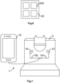
- Figure 7 represents a measurement device 7 according to the invention.
- a measurement device 7 comprises the bio-chemical sensor 5 of figure 5 and a signal analyzing unit receiving information from the photo-detector 43 and implementing a method to retrieve the signal beam amplitude and/or phase.
- the signal analyzing unit as well as the power modulation unit is implemented by a smartphone 79.
- the smartphone is thus connected to the photo-detector 43 by a first cable 793 and is connected to the optical source 40 by a second cable 790.
- the signal analyzing unit and/or the power modulation unit can also be implemented by other Consumer Electronic Devices such as computers.
- phase modulation induces a simultaneous amplitude modulation which makes it difficult to distinguish the two modulation functions, amplitude and phase, since both modulate the signal at the same frequency. Even if the signal is expressed as a sum of harmonics with Fourier decomposition, it is not trivial to simply extract an optimum signal in this case, since usually a finite number of harmonics are used to recover the amplitude or phase information.
- the signal analyzing unit comprises a lock-in amplifier and a signal processor to process data coming from the photo-detector in order to retrieve the amplitude and/or phase information.
- the lock-in amplifier works at the fundamental frequency of the modulation function and at the harmonic frequencies if present.
- the invention proposes a novel approach modifying notably the G-LIA method to solve the problem.
- the method is expressed below in the case of a sinusoidal modulation of the reference phase, which is considered as the most convenient modulation form.
- a similar approach can be followed for other types of modulation function.
- the optical source power P is thus: P t ⁇ E 1 t 2
- the first beam is split into the second beam and the reference beam and the second beam is almost entirely reflected to generate the signal beam.
- the intensity I detected by the photo-detector is proportional to the temporal average of the square of the sum of the two fields since the photo-detector is in the overlapping zone: I ⁇ ⁇ ⁇ r t + ⁇ s t 2 ⁇
- I can be expressed as: I ⁇ P 0 1 + ⁇ sin ⁇ t ⁇ 1 + m ⁇ cos a . sin ⁇ t ⁇ ⁇
- a first step is to apply a DC filter to I:
- DC 1 2 ⁇ ⁇ 0 2 ⁇ P 0 1 + ⁇ sin ⁇ t ⁇ 1 + m ⁇ cos a ⁇ sin ⁇ t ⁇ ⁇ d ⁇ t
- DC P 0 1 + 1 2 ⁇ ⁇ 0 2 ⁇ m ⁇ cos a ⁇ sin ⁇ t ⁇ ⁇ d ⁇ t + 1 2 ⁇ ⁇ 0 2 ⁇ ⁇ ⁇ sin ⁇ t d ⁇ t + 1 2 ⁇ ⁇ 0 2 ⁇ ⁇ m ⁇ 1 2 ⁇ sin ⁇ t + a ⁇ sin ⁇ t ⁇ ⁇ d ⁇ t + 1 2 ⁇ ⁇ 0 2 ⁇ ⁇ m ⁇ 1 2 ⁇ sin ⁇ t + a ⁇ sin ⁇ t ⁇ ⁇ d ⁇ t + 1 2 ⁇ ⁇ 0 2 ⁇ ⁇ m ⁇ 1 2 ⁇ sin
- amplitude m and phase ⁇ can be retrieved if the constants a and ⁇ are known for example via measurements.
- R x P 0 m 2 ⁇ cos ⁇ ⁇ k x
- R y P 0 m 2 ⁇ sin ⁇ ⁇ k y
- Amplitude m and phase ⁇ are easily retrieved from simplified R x and R y .
- the measurement device 7 further comprises a second photo-detector 43 positioned in order to receive light from the first beam B 1 and sending the information to the signal analyzing unit to exclude noise or amplitude modulation from the interference signal I.
- the measurement device 7 further comprises an additional photo-detector 43 positioned in order to receive a portion of the interference signal I, said portion being merely insensitive to the optical resonance modification occurring when a target is detected or more generally when the refractive index is changed.
- Said portion extraction is typically achieved by detecting the light polarized in a direction where the optical resonance is not perceived, known as s polarization in the case of SPR layer.
- Said portion can serve as a phase and amplitude reference to further reduce noises such as temperature dependence and vibration.
- said portion can also come from a zone insensitive to the target to serve the same purpose, for example a zone which is not functionalized. In this way, phase stability better than 10 -4 rad can be achieved in the visible range.
- the measurement device can be used for medical diagnostic via the analysis of liquids such as biological fluids, including the detection of cancer gene sequence segment(s) or virial gene segment(s) with or without the use of amplification techniques such as Polymerase Chain Reaction (PCR) or Loop-mediated isothermal amplification (LAMP), detection of cancer or virus biomarkers through the use of anti-body or aptamer.
- amplification techniques such as Polymerase Chain Reaction (PCR) or Loop-mediated isothermal amplification (LAMP), detection of cancer or virus biomarkers through the use of anti-body or aptamer.
- the sensing can focus on the presence of bacteria, pathogens, harmful chemicals, including gaseous molecules notably using cavitands, Heme groups or other polymeric materials as surface modification strategy.
- the measurement device can also be used for health prevention through bacteria detection in food for instance. The following paragraphs describe examples of possible applications.
- the proposed invention offers a good homecare platform comprising a measurement device for patients suffering from Myocardial infarction (MI) or acute myocardial infarction (AMI), commonly known as a heart attack.
- MI Myocardial infarction
- AMI acute myocardial infarction
- the measurement device monitors a proteins, Cardiac troponin I (cTnI) or troponin complex, which have been recognized as gold standard for detection of AMI.
- the optical chip can be functionalized with a specific aptameric based probe, here a DNA sequence of around 41 mer.
- the handheld detection system is therefore a measurement device comprising the optical chip functionalized with the aptameric probe, the light coupling element, typically a prism, a half-cylinder, a half-ball lens or a grating in contact with the optical chip, a photo-detector, a detection chamber and signal analyzing unit receiving information from the photo-detector and configured to retrieve the signal beam phase or amplitude, the signal analyzing unit being installed on a simple micro-controller or a smartphone for example.
- the light coupling element typically a prism, a half-cylinder, a half-ball lens or a grating in contact with the optical chip
- a photo-detector typically a prism, a half-cylinder, a half-ball lens or a grating in contact with the optical chip
- a photo-detector typically a prism, a half-
- Blood samples are typically obtained with a lancing device and may be filtered in a buffer solution, for example with nitro-cellulose (NC) membrane filtering, before introduction into the detection chamber.
- a buffer solution for example with nitro-cellulose (NC) membrane filtering
- the user can obtain a tiny drop of fingertip blood.
- the blood then is dropped into a vial, which is prefilled with a buffer solution.
- the user then drops the vial into a tailor made cassette.
- the cassette provides a sample transfer mechanism using contact force and which transfers the content of the vial into the detection chamber for final result.
- the endpoint data is read, and the result is transferred to a handheld device and demonstrated to user with a given user interface.
- Figure 8 and Figure 9 show amplitude and phase diagrams generated by the signal analyzing unit during troponin I monitoring with a measurement device according to the invention for detection of AMI.
- the binding of the aptamer on the optical chip during the functionalization step can be monitored through DNA detection.
- a typical sigmoid shape is obtained corresponding to the detection of DNA.
- a Phosphate-Buffered Saline (PBS) solution containing troponin complex (cTnI) with 10 nanomoles concentration is introduced into the detection chamber.
- PBS Phosphate-Buffered Saline
- cTnI troponin complex
- a typical sigmoid shape is obtained corresponding to the detection of cTnI.
- concentration at least one hundred times smaller can be detected in a time in the order of a few minutes or less.
- Targeted level of sensitivity to detect all relevant cases is 0.12 ng/mL of cTnI in the whole blood of a human being.
- the proposed invention offers a measurement device to detect rapidly any type of virus.
- the proposed invention offers a measurement device to detect rapidly avian influenza virus.
- Avian influenza has been one of the major pandemic in Asia as well as in Europe with H3N2 AIV in 2003. In 2004, H5N1 Avian influenza virus has led to about 293 deaths in Asia.
- AIV induces not just health care issues but also induces huge economic damages in poultry industry, notably for ducks in the south-west region in France.
- a poultry farm could establish several independent premises, with only thousands of poultries kept in a single premise to avoid cross infection during AIV pandemics.
- the proposed cost-effective handheld device offers opportunities for on-site monitoring in poultry farms.
- series of handheld sensors can be deployed in different premises within the poultry farm.
- the examiner can collect urine sample from the premises for diagnostic of AIV.
- Monolithic sensor cassette will be used to transfer sample onto the sensor using contact force.
- the detection results can be collected to a computer through a network of connected sensors.
- specific premises may undergo early culling before widespread infection occurs.
- the optical chip can be functionalized with a specific aptameric based probe, here typically Hemaglutinin 5 (H5) aptamer, a 29-mer DNA sequence.
- the handheld detection system is therefore a measurement device comprising the optical chip functionalized with the aptameric probe, the light coupling element, typically a prism, a half-cylinder, a half-ball lens or a grating in contact with the optical chip, a photo-detector, a detection chamber and signal analyzing unit receiving information from the photo-detector and configured to retrieve the signal beam phase or amplitude, the signal analyzing unit being installed on a simple micro-controller or a smartphone for example.
- urine of the poultry can be collected for test, typically after dilution in a PBS solution and NC membrane filtering.
- the proposed invention offers a measurement device to detect bacteria from any source (human food, pet food, biological and physiological samples, surface wipes).
- the sample may come from human patients suffering from Sepsis. In case of Sepsis, the patient typically has low level of immune response due to its health issue. The reduced immune response lead to different levels of bacterial infection inside body leading to Sepsis.
- the sample may come from food; the detection may serve as quality control device for vegetables or other food source to exclude samples with malicious bacteria from human ingestion.
- the measurement device can be used for detection of organic molecules, DNA or RNA, bacteria, viruses and biological markers in liquids, complex food matrices, organic matrices, food samples, tissues or blood samples, biological and physiological samples, surface wipes.
- the measurement device relies both on amplitude and on phase analysis and has therefore a better sensitivity than conventional Surface Plasmon Resonance systems relying only on amplitude analysis. Besides, the measurement device uses low cost monochromatic light sources instead of expensive spectral sources.
- the measurement device Compared to conventional protein analysis systems in biochemical laboratory done through the use of Enzyme-Linked ImmunoSorbent Assay (ELISA), the measurement device according to the invention has an increased sensitivity and saves a huge amount of time in sample preparation since a surface modification protocol taking several hours is needed for ELISA.
- ELISA Enzyme-Linked ImmunoSorbent Assay
- the measurement device according to the invention Compared to conventional Radio-Immune-Assay sensors (RIA), the measurement device according to the invention has the advantage of being suitable for on-site application.
- RIA Radio-Immune-Assay sensors
Landscapes
- Life Sciences & Earth Sciences (AREA)
- Health & Medical Sciences (AREA)
- General Physics & Mathematics (AREA)
- Physics & Mathematics (AREA)
- Chemical & Material Sciences (AREA)
- Immunology (AREA)
- Engineering & Computer Science (AREA)
- Analytical Chemistry (AREA)
- Biochemistry (AREA)
- General Health & Medical Sciences (AREA)
- Pathology (AREA)
- Hematology (AREA)
- Biomedical Technology (AREA)
- Molecular Biology (AREA)
- Urology & Nephrology (AREA)
- Biotechnology (AREA)
- Cell Biology (AREA)
- Proteomics, Peptides & Aminoacids (AREA)
- Microbiology (AREA)
- Food Science & Technology (AREA)
- Medicinal Chemistry (AREA)
- Investigating Or Analysing Materials By Optical Means (AREA)
Description
- The present invention relates generally to optical measurement devices and more particularly to a compact interferometer, a related interferometric bio-chemical sensor and a corresponding measurement device.
- Interferometry, due to its sensitivity among optical techniques, spans a wide range of applications from velocity measurement, temperature monitoring, remote sensing to bio-sensing.
-
Figure 1 and Figure 2 show respectively conventional Michelson (1) and Mach-Zehnder (2) interferometers. Referring tofigures 1 to 3b , in prior art, composing an interferometer requires an optical source (10, 20, 30), multiple mirrors (12, 12', 22, 22', 32) and beam splitters (11, 21, 21', 31, 31', 31"). The optical source emits a first beam toward a beam splitter that splits the first beam in two beams, respectively directed towards the two mirrors to obtain a reference beam after reflection on the first mirror and a signal beam after reflection on the second mirror. Said beam splitter or another beam splitter then recombines the reference beam and the signal beam to create an interference signal. Besides, a phase modulator (14, 34) is classically added to unambiguously discriminate the phase information from the amplitude information. When speed is not an issue, such phase modulator often consists of a piezo actuated mirror corresponding to the second mirror. Such arrangement allows the phase information carried by the signal beam light, to be recovered with respect to the phase of the reference beam light by processing the interference signal received by a photo-detector (13, 23, 33). - A way to confer a sensing property to an interferometer is to replace one of the mirrors by a plasmonic layer (35) coupled with a prism (36), as shown in
figure 3b . Referring tofigure 3a , the plasmonic layer (35) is functionalized, that is to say modified with a chemical probe (P) such as proteins, a specific sequence of deoxyribonucleic acid (DNA) or of ribonucleic acid (RNA) or other small molecules, in order to detect a specific marker (M) in a target solution. These chemical probes may directly detect a specific marker (M) or may undergo further bio-chemical reactions to detect a specific marker (M) or to amplify a specific marker (M) to enable detection. - An incident beam (Bi) is directed toward the plasmonic layer through a prism. Part of the incident beam induces an optical resonance (R) in the plasmonic layer and the other part is reflected to generate a signal beam (Bs). In the signal beam, some rays corresponding to a reflection angle α have undergone amplitude and phase alteration due to the optical resonance. The angle α is the resonance angle depending on the refractive index of the medium at the interface of the plasmonic layer. When markers are bound to the probes, the refractive index of the medium at the interface of the plasmonic layer changes and the surface plasmon resonance angle α is modified. This induces further amplitude and phase change of the signal beam.
- Compared to its amplitude based measurement counterpart, interferometry often offers greater sensitivity and is therefore always a great candidate for sensing or measurement systems at least in calm environments. However, such interferometers are not used for large scale applications due to the need for multiple high-tech components entailing industrial and commercial drawbacks such as complex fabrication processes, bulky device, high costs mainly due to sophisticated optical sources or piezoelectric components required for phase retrieval, and technical difficulties to obtain reliable results since optical path distance variations due to mechanical vibrations are detrimental to the quality of the phase information retrieved from the light.
- These drawbacks limit the possibility to develop a handheld interferometric device. However, the ever growing performances of Consumer Electronic Devices (CED) notably through smartphones, are pushing the development of smart physical sensors worldwide. In this context, it is clear to people in the field that compact interferometers are desirable to go one step further in metrological measurement system.
- Weight, size and cost of sensors are the typical criteria to decide whether a sensing technology is viable. Most importantly, mechanical vibrations from environment and users are inevitable which excludes possibility for conventional interferometer to be an option in the market. Lastly, even in case of laboratory scale interferometers, a monolithic interferometer offering low noise at reasonable cost is strongly desirable.
- The expanding need for portable sensors and Lab-On-Chip (LOC) system have driven a number of new solutions for compact interferometer. Examples of compact interferometric biosensors are found in the publications
US 2008/119701 A1 ,JP 2007 101242 A US 2013/329230 A1 , Y. Hadjar er al: "Compact interferometer transducer based on surface plasmon phase resonance", JOSA A, vol. 32, no. 5 (2015), p. 771 and P. Kozma et al: "Integrated planar optical waveguide interferometer biosensors: A comparative review", Biosensors and Bioelectronics, vol. 58 (2014), p. 287-307. - Some solutions use micro-structures for wave front division, while some use micro/nano-fabrication to achieve the size reduction. However, these solutions involve fine technique in fabrication and thus high costs.
- The present invention aims to propose interferometers, and related bio-chemical sensors and measurement device that demonstrate advantages including compactness, easy fabrication, use of low-cost optical source, and most importantly in term of performance, intrinsically low phase noise.
- The invention is defined in the appended claims.
- Some embodiments relate to a compact and portable interferometer comprising an optical source generating a first beam; a photo-detector receiving an interference signal; an optical chip intercepting the first beam and comprising a first reflective layer and a second reflective layer separated by a dielectric spacer layer, the first reflective layer splitting the first beam into a reference beam obtained by reflection and a second beam obtained by transmission, the second reflective layer reflecting the second beam to generate a signal beam so that the signal beam overlaps the reference beam to create the interference signal; and a controlled phase modulation means inducing a phase modulation in the interference signal by modifying the phase difference between the signal beam and the reference beam, the interferometer being characterized in that the second reflective layer is an optically-resonant layer. By optically-resonant layer we mean a surface efficiently supporting an optical mode confined at the interface of the layer. This can be typically a thin metal layer supporting a surface plasmon polariton, or a localized plasmon polariton or other dielectric resonators.
- By means of the optical chip that operates both beam splitting and beam recombination, the interferometer has a compact and monolithic design which brings low noise to the optical device.
- In some embodiments, the interferometer further comprises a support, the optical source, the optical chip and the photo-detector being fixed onto the support. The interferometer has a packaged design which makes it easily transportable. Besides, the support enables fine-tuning of angular positioning of the optical source and the photo-detector to adapt the interferometer to reflection angles of interest.
- In preferred embodiments, the dielectric spacer layer is transparent, or at least not a strongly absorbing material, with respect to the range of wavelength emission of the optical source.
- In some embodiments, the controlled phase modulation means is a wavelength modulation means inducing a phase modulation in the interference signal. For example, the interferometer comprises an optical source wavelength modulation driving unit. Since the phase difference between the reference beam and the signal beam depends on the source wavelength, the wavelength modulation induces a phase modulation in the interference signal.
- In other embodiments, the optical source is a truly tunable laser, for example a laser with external cavities offering a relative wavelength change close or higher than one percent, to create a phase modulation in the interferometer.
- In some embodiments, the wavelength modulation means is composed of an optical source power modulation unit inducing wavelength modulation in the optical source. This power modulation method utilized to create wavelength modulation in the source avoids the need for an optical source specifically designed to create wavelength modulation in a large range. Typical low-cost solid state lasers, for example monochromatic lasers from consumer electronics like VCSEL with relative wavelength change close or smaller than 10-4%, can be sufficient to create a clear phase modulation.
- In some embodiments, the dielectric spacer layer has a thickness in the range of 0.1mm to 5mm so that no delicate micro or nano-fabrication is involved which greatly facilitates the production process.
- In some embodiments, the interferometer further comprises a light conveyor, such as a prism, a fiber, a grating or a lens, to convey the light to and from the bi-reflective layer at specific angles. The incident angle of the first beam is preferably adjusted with the light conveyor to induce an optical resonance in the optically-resonant layer.
- Embodiments of the present invention further provide a bio-chemical sensor comprising an interferometer according to the invention wherein the optically-resonant layer has been chemically functionalized. By layer chemically functionalized, we mean a layer being modified with a chemical probe such as proteins, a specific sequence of deoxyribonucleic acid (DNA) or of ribonucleic acid (RNA) or other small molecules, in order to detect a specific marker in a target solution.
- In some embodiments, the bio-chemical sensor further comprises a detection chamber attached to the optically-resonant layer and aimed to receive an analyte to be analyzed by said bio-chemical sensor. The detection chamber consists of a space that can be filled with an analyte such as a fluid. It may be a micro-fluidic channel, a gas perfusion channel, or simply an open cuvette. The detection chamber carries the target solution or gas to the optically-resonant layer surface.
- In some embodiments, the optically-resonant layer comprises a plurality of distinct sub-areas arranged in a plane, different resonance properties or different functionalizations being associated to said distinctive sub-areas; and the photo-detector is arranged to receive an interference signal from each sub-area, typically using a quadrant photodiode, a linear Charged-Coupled Device (CCD), a 2D CCD, or similar detector based on Complementary Metal-Oxide Semiconductor technology (CMOS). Detecting multiple bio-markers in a diagnostic improves screening capabilities by increasing the number of test performed at once. As for traditional, amplitude based measurements, the use of a linear or 2D CCD or CMOS detector can also be used to detect light impinging on the sensing surface at different angles.
- Embodiments of the present invention further provide a measurement device comprising an interferometer or a bio-chemical sensor according to the invention; and a signal analyzing unit receiving information from the photo-detector and configured to retrieve the signal beam amplitude and/or phase.
- In some embodiments, the measurement device is used for monitoring Cardiac troponin I (cTnI) and the optical chip has been functionalized with a cTnI aptameric probe. The aptameric probe is comprised of specific sequences of DNA codon with one of its end being capable to bind onto the plasmonic layer for example using thiols to bind on a gold surface, or using thiol-ene click reaction or other chemical means.
- In some embodiments, the measurement device is used for detection of avian influenza virus and the optical chip has been functionalized with a Hemaglutinin 5 (H5) aptamer. The aptameric probe is comprised of specific sequence of DNA codon with one of its end being capable to bind onto the plasmonic layer for example thiol gold reaction, thiol-ene click reaction or other chemical means.
- In some embodiments, the measurement device is used for detection of bacteria and the optical chip has been functionalized with a specific probe.
- In some embodiments, the measurement device further comprises a second photo-detector positioned in order to receive light from the first beam and sending information to the signal analyzing unit to exclude noise or amplitude modulation from the interference signal.
- In some embodiments, the measurement device further comprises an additional photo-detector positioned in order to receive a portion of the interference signal, said portion being merely insensitive to the optical resonance, and sending information to the signal analyzing unit to exclude noise or amplitude modulation from the interference signal. For example, the s-polarized part of the light can be used a phase reference to correct the impact of influence quantities such as temperature.
- In some embodiments, the power modulation unit and/or the signal analyzing unit are implemented by one or more portable Consumer Electronic Devices.
- Additional aspects of embodiments will be set forth, in part, in the detailed description, figures and any claims which follow, and in part will be derived from the detailed description. It is to be understood that both the foregoing general description and the following detailed description are only exemplary and do not limit the claimed invention, which is defined in the appended claims.
- Some embodiments of apparatus and/or methods will become more fully understood from the detailed description given herein below and the accompanying drawings which are given by way of illustration only and thus are not limiting of the present invention and wherein:
-
Figure 1 is a schematic illustration of a conventional Michelson interferometer in prior art; -
Figure 2 is a schematic illustration of a conventional Mach-Zehnder interferometer in prior art; -
Figure 3a schematically depicts the principle of a Surface Plasmon Resonance sensor in prior art; -
Figure 3b schematically represents an interferometric Surface Plasmon Resonance sensor in prior art; -
Figure 4 is a schematic view of a compact optically-resonant interferometer according to present invention; -
Figure 5 is a schematic view of an interferometric bio-chemical sensor according to present invention; -
Figure 6 is a schematic top view of an optically-resonant layer structured into several separated sub-area with different resonance properties and different functionalizations; -
Figure 7 is a schematic view of a measurement device comprising a portable Consumer Electronic Device to process optical information; -
Figure 8 is an amplitude and phase diagram generated during the binding of DNA on the optically-resonant layer using the measurement device according to the invention; and -
Figure 9 shows troponin complex monitoring with a measurement device according to the invention for detection of AMI. - While example embodiments are capable of various modifications and alternative forms, embodiments thereof are shown by way of example in the drawings and will herein be described in details. It should be understood, however, that there is no intent to limit example embodiments to the particular forms disclosed, but on the contrary, example embodiments are to cover all modifications, equivalents, and alternatives falling within the scope of the claims. Like numbers refer to like elements throughout the description of the figures.
-
Figure 4 depicts an interferometer 4 according to the invention. The interferometer 4 comprises anoptical source 40, an optical chip, a photo-detector 43 and asupport 48 on which all the above components are fixed. - The
optical source 40 has sufficient spectral coherence to be used in interferometry. Theoptical source 40 is typically a laser diode or a VCSEL. If needed, theoptical source 40 is equipped with optical isolator or polarization control. - The optical chip is typically a bi-reflective layer made of isotropic and dielectric transparent materials such as optical or classical glass, plastics or organic materials. Such a bi-reflective layer offers at least two reflective surfaces at the interfaces of the layer with mediums of different refractive index. The optical chip is usually coupled with a
light conveyor 46, for example a prism, a fiber, a grating or a lens, to convey the light to and from the bi-reflective layer at specific angles. The light conveyor refractive index may be the same as the one of the bi-reflective layer. In this case, no reflection would occur at the interface between the bi-reflective layer and the conveyor without depositing a thin reflective layer on this interface. In a best mode, the reflectance of the reflective surfaces is enhanced by depositing a thin reflective layer on these interfaces. On this basis, the optical chip is described as a firstreflective layer 42 and a secondreflective layer 45 separated by adielectric spacer layer 41. - In a best mode, especially when the light from the optical source is diverging, the light conveyor is a half-ball lens collimating the first beam so that all the rays of the first beam are impinging near the center of the half-ball at the same incident angle on the optical chip. The use of a half-ball avoids the refraction angle produced at air-prism interface, ensuring consistent illumination condition if the angle is varied. This mode provides good measurement results even if the optical source used has poor collimation properties for example in the case of a low cost optical source.
- The
optical source 40 generates a first beam B1 which is conveyed toward the firstreflective layer 42 by a prism. The firstreflective layer 42 splits the first beam B1 into a reference beam BR obtained by reflection and a second beam B2 obtained by transmission, the secondreflective layer 45 reflects the second beam B2 to generate a signal beam BS that overlaps the reference beam BR to create an interference signal I. - In order to implement phase retrieval method, the interferometer 4 comprises an optical source wavelength modulation means 44. Since the phase difference between the reference beam BR and the signal beam BS depends on the source wavelength, the wavelength modulation induces a phase modulation in the interference signal I. A first solution for wavelength modulation is to use a truly tunable laser, for example a laser with external cavities offering a relative wavelength change close or higher than one percent, as an
optical source 40. Such lasers enable phase modulation in the interferometer 4. A second low cost solution for wavelength modulation is to use an optical source power modulation unit inducing a slight wavelength modulation in theoptical source 40. Power modulation can be achieved by modulating the supply electric current in theoptical source 40. This solution avoids the need for anoptical source 40 specifically designed to create wavelength modulation in a large range. Typical low-cost solid state lasers, for example lasers from consumer electronics like VCSEL with relative wavelength change close or smaller than 10-4%, can be sufficient to create a clear phase modulation, in the order or higher than one radian, for reasonably largedielectric spacer 41, as detailed hereafter. - Unless the angle of incidence is small, the thickness of the
dielectric spacer layer 41 is preferably smaller than the beam diameter coming from theoptical source 40, in order to obtain sufficient overlap between the reference beam BR and the signal beam BS. However, the thickness of thedielectric spacer layer 41 must be thick enough to measure a clear variation in the interference signal I due to phase modulation. The fundamental reason for having a thick enough spacer is that the phase modulation achieved by the apparatus will be proportional to this thickness and that a small modulation will result in a weak and possibly noisy signal. The thickness of the above mentionedspacer layer 41 must render phase interrogation possible with plausible range of output power modulation foroptical source 40. Typically, the thickness of the above mentionedspacer layer 41 is much larger than microscale so that no tedious micro-fabrication is required. In addition, low cost optical sources that exhibit little degree of wavelength modulation are preferable. For such typical lasers working in the visible or near-infrared range, convenient spacer thicknesses in the 0.1mm to 5mm range can therefore be used, with some variations depending on the material refractive index, exact wavelength and angle of incidence. Larger wavelengths require larger thickness. - The photo-
detector 43 receives the interference signal I. In this configuration, a single active area is sufficient and the photo-detector 43 is typically a single photodiode. However, a two dimensional detection device such as a CCD camera is also adapted. Based on Nyquist Sampling theorem, the photo-detector 43 has an acquisition rate at least twice times higher than the optical source wavelength modulation frequency. - The
support 48 is preferably monolithic, compact and portable. Thesupport 48 is made of rigid plastic or wood for example. Even if thesupport 48 is made of several elements, the interferometer can be regarded as monolithic since the heart of the interferometer, the bi-reflective optical chip, that splits and recombines the beam is a single element. - In some embodiments that are not represented, the optical source and the photo-detector positions are adjustable. For example, the support comprises two arms connected by a hinge, like a compass, in a pivot linkage with the support. The optical source and the photo-detector are placed respectively on each arm to enable fine-tuning of the angles of light emission and light reception. Said angles fine-tuning can be automatic, semi-automatic or manual.
- According to the invention, the second
reflective layer 45 is an optically-resonant layer. Under a predefined angle depending on the refractive index of the medium at the interface of the optically-resonant layer and on the optically-resonant layer characteristics, incident light induces an optical resonance R confined at the interface of the optically-resonant layer. The optically-resonant layer is typically a thin metal layer, usually smaller than the light wavelength in height, supporting a surface plasmon polariton. However said layer can also support a localized surface plasmon polariton (LSPP) or Dielectric Resonators (DR). LSPP or DR can increase the optical resonance and therefore increase the interferometer sensitivity to changes occurring at the layer interface. To achieve LSPP or DR, the optically resonant layer can be structured. - In
figure 4 , part of the second beam B2 elicits an optical resonance R in the optically-resonant layer and the rest of the second beam B2 is reflected toward the photo-detector 43 to generate the signal beam BS. - The incident angle of the first beam B1 is preferably adjusted with the
light conveyor 46 to induce an optical resonance R in the optically-resonant layer. If there is no clear optical resonant in the said layer, as for a bare dielectric surface, it is preferable to choose an angle large enough to be above the critical angle in order to still have a confined mode with an evanescent wave at the interface of the secondreflective layer 45. -
Figure 5 depicts abio-chemical sensor 5 according to the invention. Thebio-chemical sensor 5 comprises the interferometer 4 offigure 4 wherein the optically-resonant layer has been chemically functionalized that is to say modified with a chemical probe P such as proteins, a specific sequence of deoxyribonucleic acid (DNA) or of ribonucleic acid (RNA) or other small molecules, in order to detect a specific marker (M) in a target solution. These chemical probes may directly detect a specific marker (M) or may undergo further bio-chemical reactions to detect a specific marker (M) or to amplify a specific marker (M) to enable detection. - The
bio-chemical sensor 5 further comprises adetection chamber 57 attached to the optically-resonant layer and aimed to receive an analyte. Thedetection chamber 57 consists of a space that can be filled with an analyte such as a fluid. It may be a micro-fluidic channel, a gas perfusion channel, or simply an open cuvette. Thedetection chamber 57 carries the target solution or gas to the optically-resonant layer surface. Preferably, thedetection chamber 57 comprises an inlet 571 and an outlet 572. - Referring to
figure 6 , the optically-resonant layer has been structured into several separated sub-area 650 with different resonance properties or different functionalizations in order to detect multiple bio-markers. In this example, such an optically-resonant layer is an array of plasmonic films and is referred as aplasmonic array layer 65. Each element surface in theplasmonic array layer 65 is preferably composed of the same plasmonic material with same film and resonance properties to simplify fabrication. However, the functionalization can differ from one point to the other. Nevertheless, theplasmonic array layer 65 design may be tailored to different sensing purposes. For example, theplasmonic array layer 65 design can be an array of grid, a grid being composed of nanoparticles arranged according to a pattern, with each grid having different resonance properties by use of Localized Surface Plasmon Resonance (LSPR) induced by nano-particle inside the grid. Theplasmonic array layer 65 can also be a gold or silver film grid array made by one evaporation process with shadow mask. The above mentionedplasmonic array layer 65 designs are given as examples and should not be regarded as limitations, in particular regarding the grid pattern on the layer. - In
figure 6 embodiment, the photo-detector 43 has to be tailored to receive an interference signal I from each sub-area 650. For example, the photo-detector 43 is a camera or a photo-detector array, that is to say an array of photo-detectors that are aligned to receive the interference signal I from each plasmonic film grid of theplasmonic array layer 65. -
Figure 7 represents ameasurement device 7 according to the invention. Such ameasurement device 7 comprises thebio-chemical sensor 5 offigure 5 and a signal analyzing unit receiving information from the photo-detector 43 and implementing a method to retrieve the signal beam amplitude and/or phase. The signal analyzing unit as well as the power modulation unit is implemented by asmartphone 79. The smartphone is thus connected to the photo-detector 43 by afirst cable 793 and is connected to theoptical source 40 by asecond cable 790. The signal analyzing unit and/or the power modulation unit can also be implemented by other Consumer Electronic Devices such as computers. - Actually, only few methods among which Generalized Lock-In Amplifier (G-LIA, described in the article Generalized lock-in detection for interferometry: application to phase sensitive spectroscopy and near-field nanoscopy published by OSA in Optics Express Vol. 22, Issue 18, pp. 22232-22245, also detailed in the patent applications
FR301055 PCT2015036699 US2015070704 ) have been proposed to recover the phase information with arbitrary continuous phase modulation. Alternately, methods based on multiple harmonics detection can be used to recover the phase information in the specific case of a continuous sinusoidal phase modulation. These methods require constant amplitude during phase modulation. Unless the setup offers the possibility to normalize the amplitude, such aspect complicates the analysis and might be the reason why no similar approach has been proposed previously. To state it clearly, the specific additional difficulty here is that the phase modulation induces a simultaneous amplitude modulation which makes it difficult to distinguish the two modulation functions, amplitude and phase, since both modulate the signal at the same frequency. Even if the signal is expressed as a sum of harmonics with Fourier decomposition, it is not trivial to simply extract an optimum signal in this case, since usually a finite number of harmonics are used to recover the amplitude or phase information. - In this example, the signal analyzing unit comprises a lock-in amplifier and a signal processor to process data coming from the photo-detector in order to retrieve the amplitude and/or phase information. The lock-in amplifier works at the fundamental frequency of the modulation function and at the harmonic frequencies if present.
- The invention proposes a novel approach modifying notably the G-LIA method to solve the problem. The method is expressed below in the case of a sinusoidal modulation of the reference phase, which is considered as the most convenient modulation form. A similar approach can be followed for other types of modulation function.
- The optical source signal ε1, that is to say the first beam signal, is expressed as follows:

- The optical source power P is thus:

- The first beam is split into the second beam and the reference beam and the second beam is almost entirely reflected to generate the signal beam.
- Using same type of notations as for ε1, the reference beam signal εr and the signal beam signal εs are expressed as follows:


- With these notations, the intensity I detected by the photo-detector is proportional to the temporal average of the square of the sum of the two fields since the photo-detector is in the overlapping zone:

- Considering that the amplitude and phases variations are slow compared to ω:

- Besides, Er(t) and Es(t) can be written as follows:


- Thus:

- With P(t) = E 1(t)2 and m=2rs:

- The later relation is true for any phase modulation of the reference beam ϕr (t). As mentioned, we consider the case of a sinusoidal phase modulation induced by a sinusoidal power modulation P(t) of the optical source:

- And so:

- Besides, ϕr - ϕs depends on:
- the optical path difference L between the reference beam and the signal beam,
- the phase modification due to reflection on the first reflective layer which is constant, and
- the phase modification ϕ due to resonance which is the phase information that is monitored.
- This phase difference Φ due to the optical path difference L can be calculated as follows:

- e: the thickness of the dielectric spacer layer,
- n: the refractive index of dielectric spacer layer,
- θ: the angle of the transmitted beam inside the dielectric spacer, with respect to the normal of the first reflective layer,
- λ: the free space wavelength of the optical source.
- As power modulation induces a wavelength modulation, the wavelength λ can be written as follows:

- Where the second term is a very small modulation compared to λ 0. Then, Φ can be written as Φ = Φ 0 + dΦ where Φ0 is constant and


- Constant terms can be ignored and I can be expressed as:

- In order to retrieve the phase information ϕ, a first step is to apply a DC filter to I:


- Bessel functions are introduced:


- Thus

- After applying the DC filter, Ifilter can be written as follows:

- To recover amplitude and phase, an efficient approach is to perform a G-LIA on Ifilter to get:


- After calculation, Rx and Ry can be expressed as:


- From the above expressions, amplitude m and phase ϕ can be retrieved if the constants a and µ are known for example via measurements.
- Rx and Ry can be simplified by setting the phase modulation depth


- Amplitude m and phase ϕ are more easily retrieved from these simplified Rx and Ry. In addition, simulations and experiences show that, provided µ ≤ 0.1, µ·sin(ϕ)·J 1(2a) and µ·cos(ϕ)·J 1(2a) can be neglected.
- Finally, very simple expressions are obtained for Rx and Ry:


- With:


- Amplitude m and phase ϕ are easily retrieved from simplified Rx and Ry.
- The original above method has been detailed for a sinusoidal power modulation function. This amplitude and phase extraction method can be performed by adequate CED such as microcontrollers, or smartphones, for example via the audio Jack plug for analog signals. Similar extraction approaches exist with a sawtooth power modulation function or other continuous wavelength modulation functions. In complex cases, calculations may involve the determination of at least one even and one odd harmonics of the interference signal I to retrieve the phase. For pure wavelength modulation, with constant or quasi constant optical source power, calculations can be simplified, and the mentioned GLIA method can be used more straightforwardly.
- In some embodiments, the
measurement device 7 further comprises a second photo-detector 43 positioned in order to receive light from the first beam B1 and sending the information to the signal analyzing unit to exclude noise or amplitude modulation from the interference signal I. - In some embodiments, the
measurement device 7 further comprises an additional photo-detector 43 positioned in order to receive a portion of the interference signal I, said portion being merely insensitive to the optical resonance modification occurring when a target is detected or more generally when the refractive index is changed. Said portion extraction is typically achieved by detecting the light polarized in a direction where the optical resonance is not perceived, known as s polarization in the case of SPR layer. Said portion can serve as a phase and amplitude reference to further reduce noises such as temperature dependence and vibration. When multiple zones are analyzed, said portion can also come from a zone insensitive to the target to serve the same purpose, for example a zone which is not functionalized. In this way, phase stability better than 10-4 rad can be achieved in the visible range. - A large number of sensing applications can be targeted by the invention, for example the measurement device can be used for medical diagnostic via the analysis of liquids such as biological fluids, including the detection of cancer gene sequence segment(s) or virial gene segment(s) with or without the use of amplification techniques such as Polymerase Chain Reaction (PCR) or Loop-mediated isothermal amplification (LAMP), detection of cancer or virus biomarkers through the use of anti-body or aptamer. Alternately, the sensing can focus on the presence of bacteria, pathogens, harmful chemicals, including gaseous molecules notably using cavitands, Heme groups or other polymeric materials as surface modification strategy. The measurement device can also be used for health prevention through bacteria detection in food for instance. The following paragraphs describe examples of possible applications.
- As a first example of a possible application, the proposed invention offers a good homecare platform comprising a measurement device for patients suffering from Myocardial infarction (MI) or acute myocardial infarction (AMI), commonly known as a heart attack. Conventionally, AMI can be detected through Electro-cardiogram. However the sensitivity of the diagnostic is not good with only 57% of patients being diagnosed correctly. The measurement device monitors a proteins, Cardiac troponin I (cTnI) or troponin complex, which have been recognized as gold standard for detection of AMI.
- For the measurement device to detect cTnI, the optical chip can be functionalized with a specific aptameric based probe, here a DNA sequence of around 41 mer. The handheld detection system is therefore a measurement device comprising the optical chip functionalized with the aptameric probe, the light coupling element, typically a prism, a half-cylinder, a half-ball lens or a grating in contact with the optical chip, a photo-detector, a detection chamber and signal analyzing unit receiving information from the photo-detector and configured to retrieve the signal beam phase or amplitude, the signal analyzing unit being installed on a simple micro-controller or a smartphone for example.
- Blood samples are typically obtained with a lancing device and may be filtered in a buffer solution, for example with nitro-cellulose (NC) membrane filtering, before introduction into the detection chamber. For example, with the help of a lancing device, the user can obtain a tiny drop of fingertip blood. The blood then is dropped into a vial, which is prefilled with a buffer solution. The user then drops the vial into a tailor made cassette. The cassette provides a sample transfer mechanism using contact force and which transfers the content of the vial into the detection chamber for final result. After a predetermined waiting time, the endpoint data is read, and the result is transferred to a handheld device and demonstrated to user with a given user interface.
-
Figure 8 and Figure 9 show amplitude and phase diagrams generated by the signal analyzing unit during troponin I monitoring with a measurement device according to the invention for detection of AMI. As a first step, shown inFigure 8 , the binding of the aptamer on the optical chip during the functionalization step can be monitored through DNA detection. A typical sigmoid shape is obtained corresponding to the detection of DNA. As a second step, shown inFigure 9 , when the probe DNA is attached, a Phosphate-Buffered Saline (PBS) solution containing troponin complex (cTnI) with 10 nanomoles concentration is introduced into the detection chamber. A typical sigmoid shape is obtained corresponding to the detection of cTnI. From the obtained sensitivity, concentration at least one hundred times smaller can be detected in a time in the order of a few minutes or less. Targeted level of sensitivity to detect all relevant cases is 0.12 ng/mL of cTnI in the whole blood of a human being. - As a second example of a possible application, the proposed invention offers a measurement device to detect rapidly any type of virus. For example, the proposed invention offers a measurement device to detect rapidly avian influenza virus. Avian influenza has been one of the major pandemic in Asia as well as in Europe with H3N2 AIV in 2003. In 2004, H5N1 Avian influenza virus has led to about 293 deaths in Asia. AIV induces not just health care issues but also induces huge economic damages in poultry industry, notably for ducks in the south-west region in France. Typically, a poultry farm could establish several independent premises, with only thousands of poultries kept in a single premise to avoid cross infection during AIV pandemics. In the above mentioned context, the proposed cost-effective handheld device offers opportunities for on-site monitoring in poultry farms. As sensors according to the invention are affordable, series of handheld sensors can be deployed in different premises within the poultry farm. The examiner can collect urine sample from the premises for diagnostic of AIV. Monolithic sensor cassette will be used to transfer sample onto the sensor using contact force. The detection results can be collected to a computer through a network of connected sensors. In case of infection, specific premises may undergo early culling before widespread infection occurs.
- To detect avian influenza, the optical chip can be functionalized with a specific aptameric based probe, here typically Hemaglutinin 5 (H5) aptamer, a 29-mer DNA sequence. The handheld detection system is therefore a measurement device comprising the optical chip functionalized with the aptameric probe, the light coupling element, typically a prism, a half-cylinder, a half-ball lens or a grating in contact with the optical chip, a photo-detector, a detection chamber and signal analyzing unit receiving information from the photo-detector and configured to retrieve the signal beam phase or amplitude, the signal analyzing unit being installed on a simple micro-controller or a smartphone for example. In this case urine of the poultry can be collected for test, typically after dilution in a PBS solution and NC membrane filtering.
- As a third example of a possible application, the proposed invention offers a measurement device to detect bacteria from any source (human food, pet food, biological and physiological samples, surface wipes). In one example, the sample may come from human patients suffering from Sepsis. In case of Sepsis, the patient typically has low level of immune response due to its health issue. The reduced immune response lead to different levels of bacterial infection inside body leading to Sepsis. In another example, the sample may come from food; the detection may serve as quality control device for vegetables or other food source to exclude samples with malicious bacteria from human ingestion.
- As other examples of possible applications, the measurement device can be used for detection of organic molecules, DNA or RNA, bacteria, viruses and biological markers in liquids, complex food matrices, organic matrices, food samples, tissues or blood samples, biological and physiological samples, surface wipes.
- The measurement device according to the invention relies both on amplitude and on phase analysis and has therefore a better sensitivity than conventional Surface Plasmon Resonance systems relying only on amplitude analysis. Besides, the measurement device uses low cost monochromatic light sources instead of expensive spectral sources.
- Compared to conventional protein analysis systems in biochemical laboratory done through the use of Enzyme-Linked ImmunoSorbent Assay (ELISA), the measurement device according to the invention has an increased sensitivity and saves a huge amount of time in sample preparation since a surface modification protocol taking several hours is needed for ELISA.
- Compared to conventional Radio-Immune-Assay sensors (RIA), the measurement device according to the invention has the advantage of being suitable for on-site application.
- Although some embodiments of the present invention have been illustrated in the accompanying Drawings and described in the foregoing Detailed Description, it should be understood that the present invention is not limited to the disclosed embodiments, but is capable of numerous modifications without departing from the invention as set forth and defined by the following claims.
Claims (12)
- Interferometer (4) comprising:- an optical source (40) configured to generate a first beam (B1);- a photo-detector (43) configured to receive an interference signal (I);- a monolithic optical chip configured to intercept the first beam (B1), that is a bi-reflective layer offering at least two reflective surfaces at the interfaces of the bi-reflective layer with mediums of different refractive index and comprising a first top reflective layer (42) and a second bottom reflective layer (45) separated by an intermediary isotropic and dielectric spacer layer (41), the first top reflective layer (42) splitting the first beam (B1) into a reference beam (BR) obtained by reflection and a second beam (B2) obtained by transmission, the second bottom reflective layer (45) being an optically-resonant layer reflecting the second beam (B2) to generate a signal beam (BS) so that the signal beam (BS) overlaps the reference beam (BR) to create the interference signal (I); characterized in that it further comprises a controlled phase modulation means configured to induce a phase modulation in the interference signal (I) by modifying the phase difference between the signal beam (Bs) and the reference beam (BR).
- Interferometer (4) according to claim 1 further comprising a support (48), the optical source (40), the optical chip and the photo-detector (43) being fixed onto the support (48).
- Interferometer (4) according to claim 1 or 2 wherein the controlled phase modulation means is a wavelength modulation means (44) inducing a phase modulation in the interference signal (I).
- Interferometer (4) according to claim 3 wherein the wavelength modulation means (44) is composed of an optical source power modulation unit inducing wavelength modulation in the optical source (40).
- Interferometer (4) according to any one of claims 1 to 4 further comprising a light conveyor (46) to convey the light to and from the bi-reflective layer at specific angles.
- Bio-chemical sensor (5) characterized in that it comprises an interferometer (4) according to any one of claims 1 to 5 wherein the second bottom optically-resonant layer (45) has been chemically functionalized.
- Bio-chemical sensor (5) according to claim 6 further comprising a detection chamber (57) attached to the lower surface of the second bottom optically-resonant layer and aimed to receive an analyte to be analyzed by said bio-chemical sensor.
- Bio-chemical sensor (5) according to claim 6 or 7 wherein:- the optically-resonant second bottom layer (45) comprises a plurality of distinct sub-areas (650), different resonance properties or different functionalizations being associated to said distinct sub-areas (650); and- the photo-detector (43) is arranged to receive an interference signal (I) from each sub-area (650).
- Measurement device (7) characterized in that it comprises:- an interferometer (4) according to any one of claims 1 to 5 or a bio-chemical sensor (5) according to any one of claims 6 to 8; and- a signal analyzing unit receiving information from the photo-detector (43) and configured to retrieve the signal beam (BS) amplitude and/or phase.
- Measurement device (7) according to claim 9 for monitoring Cardiac troponin I (cTnI) wherein the optical chip has been functionalized with a cTnI aptameric probe.
- Measurement device (7) according to claim 9 for detection of avian influenza virus wherein the optical chip has been functionalized with a Hemaglutinin 5 (H5) aptamer.
- Measurement device (7) according to claim 9 for detection of bacteria wherein the optical chip has been functionalized with a specific probe.
Applications Claiming Priority (2)
| Application Number | Priority Date | Filing Date | Title |
|---|---|---|---|
| PCT/EP2016/054852 WO2017152946A1 (en) | 2016-03-08 | 2016-03-08 | Compact interferometer, related bio-chemical sensor and measurement device |
| PCT/EP2017/055269 WO2017153378A1 (en) | 2016-03-08 | 2017-03-07 | Compact interferometer, related bio-chemical sensor and measurement device |
Publications (3)
| Publication Number | Publication Date |
|---|---|
| EP3427003A1 EP3427003A1 (en) | 2019-01-16 |
| EP3427003B1 true EP3427003B1 (en) | 2023-11-01 |
| EP3427003C0 EP3427003C0 (en) | 2023-11-01 |
Family
ID=55484995
Family Applications (1)
| Application Number | Title | Priority Date | Filing Date |
|---|---|---|---|
| EP17709074.3A Active EP3427003B1 (en) | 2016-03-08 | 2017-03-07 | Compact interferometer, related bio-chemical sensor and measurement device |
Country Status (2)
| Country | Link |
|---|---|
| EP (1) | EP3427003B1 (en) |
| WO (2) | WO2017152946A1 (en) |
Families Citing this family (7)
| Publication number | Priority date | Publication date | Assignee | Title |
|---|---|---|---|---|
| FR3090099B1 (en) | 2018-12-18 | 2022-04-22 | Univ De Technologie De Troyes | LASER DEVICE FOR POLARIZATION INTERFEROMETRY |
| US12196672B2 (en) | 2020-05-07 | 2025-01-14 | Hand Held Products, Inc. | Apparatuses, systems, and methods for sample testing |
| US12553885B2 (en) | 2020-05-07 | 2026-02-17 | Hand Held Products, Inc. | Apparatuses, systems, and methods for sample testing |
| US12498328B2 (en) | 2020-05-07 | 2025-12-16 | Hand Held Products, Inc. | Apparatuses, systems, and methods for sample testing |
| US11846574B2 (en) | 2020-10-29 | 2023-12-19 | Hand Held Products, Inc. | Apparatuses, systems, and methods for sample capture and extraction |
| WO2022232096A1 (en) * | 2021-04-26 | 2022-11-03 | Salvus, Llc | Systems and methods for chemical and biological authentication |
| CN114414489B (en) * | 2022-01-26 | 2023-07-21 | 黄淮学院 | A SF6 Gas Optical Sensing Information Monitoring System |
Family Cites Families (5)
| Publication number | Priority date | Publication date | Assignee | Title |
|---|---|---|---|---|
| JP2007101242A (en) * | 2005-09-30 | 2007-04-19 | Fujifilm Corp | Sensing device |
| US8280470B2 (en) * | 2006-11-03 | 2012-10-02 | Volcano Corporation | Analyte sensor method and apparatus |
| US9285314B2 (en) * | 2011-10-12 | 2016-03-15 | Brown University | Systems and methods enabling high-throughput, real time detection of analytes |
| US8953168B2 (en) * | 2012-06-08 | 2015-02-10 | City University Of Hong Kong | Optical sensing devices and methods for detecting samples using the same |
| FR3010555B1 (en) | 2013-09-11 | 2019-12-20 | Universite De Technologie De Troyes | ELECTRONIC PROCESS FOR EXTRACTING THE AMPLITUDE AND PHASE OF A SIGNAL IN A SYNCHRONOUS DETECTION AND ITS APPLICATION IN INTERFEROMETRIC MOUNTS. |
-
2016
- 2016-03-08 WO PCT/EP2016/054852 patent/WO2017152946A1/en not_active Ceased
-
2017
- 2017-03-07 WO PCT/EP2017/055269 patent/WO2017153378A1/en not_active Ceased
- 2017-03-07 EP EP17709074.3A patent/EP3427003B1/en active Active
Also Published As
| Publication number | Publication date |
|---|---|
| EP3427003C0 (en) | 2023-11-01 |
| WO2017153378A1 (en) | 2017-09-14 |
| WO2017152946A1 (en) | 2017-09-14 |
| EP3427003A1 (en) | 2019-01-16 |
Similar Documents
| Publication | Publication Date | Title |
|---|---|---|
| EP3427003A1 (en) | Compact interferometer, related bio-chemical sensor and measurement device | |
| Lin et al. | Intensity-detection-based guided-mode-resonance optofluidic biosensing system for rapid, low-cost, label-free detection | |
| EP2449363B1 (en) | Optical sensing device and method for detecting samples | |
| Washburn et al. | Photonics-on-a-chip: recent advances in integrated waveguides as enabling detection elements for real-world, lab-on-a-chip biosensing applications | |
| US5229833A (en) | Optical sensor | |
| Rho et al. | Label-free optical resonator-based biosensors | |
| Jha et al. | Label-free biochemical sensing using processed optical fiber interferometry: a review | |
| US20140080729A1 (en) | Optical sensing device for sensing analytes and related apparatus and methods | |
| Sypabekova et al. | Ultralow limit detection of soluble HER2 biomarker in serum with a fiber-optic ball-tip resonator assisted by a tilted FBG | |
| Barrios | Integrated microring resonator sensor arrays for labs-on-chips | |
| EP2443438B1 (en) | A surface plasmon resonance sensing method and sensing system | |
| You et al. | Highly sensitive detection of biological substances using microfluidic enhanced Fabry-Perot etalon-based optical biosensors | |
| CN115096829B (en) | Optical fiber biosensor, biological detection device and detection method thereof | |
| Qu et al. | Application of optical fiber sensing technology and coating technology in blood component detection and monitoring | |
| US20140233039A1 (en) | Physical/chemical sensor, physical/chemical phenomenon sensing device, and method for manufacturing same | |
| US20110244588A1 (en) | Optical detection systems and methods of making and using the same | |
| JP4999707B2 (en) | Method for surface plasmon spectroscopy in a surface plasmon resonance sensor and element for its use | |
| Bryan et al. | A multiplex “Disposable Photonics” biosensor platform and its application to antibody profiling in upper respiratory disease | |
| KR101249754B1 (en) | Ringresonator sensor including asymmetric mach-zehnder interferometer, self-reference waveguide including the same and microresonator apparatuses for sensing including the same | |
| US20110242542A1 (en) | Fringe locking subsystem and methods of making and using the same | |
| CN106442419B (en) | Self compensation SPR optical fiber biochemical sensor | |
| Wiki et al. | Compact integrated optical sensor system | |
| Tabbakh et al. | Optoelectronics and Optical | |
| CN103994978A (en) | Label-free light reflection interference optical fiber biosensor | |
| CN115406869A (en) | High-sensitivity U-shaped metal super-surface biosensor and use method thereof |
Legal Events
| Date | Code | Title | Description |
|---|---|---|---|
| STAA | Information on the status of an ep patent application or granted ep patent |
Free format text: STATUS: UNKNOWN |
|
| STAA | Information on the status of an ep patent application or granted ep patent |
Free format text: STATUS: THE INTERNATIONAL PUBLICATION HAS BEEN MADE |
|
| PUAI | Public reference made under article 153(3) epc to a published international application that has entered the european phase |
Free format text: ORIGINAL CODE: 0009012 |
|
| STAA | Information on the status of an ep patent application or granted ep patent |
Free format text: STATUS: REQUEST FOR EXAMINATION WAS MADE |
|
| 17P | Request for examination filed |
Effective date: 20181008 |
|
| AK | Designated contracting states |
Kind code of ref document: A1 Designated state(s): AL AT BE BG CH CY CZ DE DK EE ES FI FR GB GR HR HU IE IS IT LI LT LU LV MC MK MT NL NO PL PT RO RS SE SI SK SM TR |
|
| AX | Request for extension of the european patent |
Extension state: BA ME |
|
| DAV | Request for validation of the european patent (deleted) | ||
| DAX | Request for extension of the european patent (deleted) | ||
| STAA | Information on the status of an ep patent application or granted ep patent |
Free format text: STATUS: EXAMINATION IS IN PROGRESS |
|
| 17Q | First examination report despatched |
Effective date: 20210525 |
|
| GRAP | Despatch of communication of intention to grant a patent |
Free format text: ORIGINAL CODE: EPIDOSNIGR1 |
|
| STAA | Information on the status of an ep patent application or granted ep patent |
Free format text: STATUS: GRANT OF PATENT IS INTENDED |
|
| INTG | Intention to grant announced |
Effective date: 20221215 |
|
| GRAS | Grant fee paid |
Free format text: ORIGINAL CODE: EPIDOSNIGR3 |
|
| GRAA | (expected) grant |
Free format text: ORIGINAL CODE: 0009210 |
|
| STAA | Information on the status of an ep patent application or granted ep patent |
Free format text: STATUS: THE PATENT HAS BEEN GRANTED |
|
| AK | Designated contracting states |
Kind code of ref document: B1 Designated state(s): AL AT BE BG CH CY CZ DE DK EE ES FI FR GB GR HR HU IE IS IT LI LT LU LV MC MK MT NL NO PL PT RO RS SE SI SK SM TR |
|
| REG | Reference to a national code |
Ref country code: GB Ref legal event code: FG4D |
|
| REG | Reference to a national code |
Ref country code: CH Ref legal event code: EP |
|
| REG | Reference to a national code |
Ref country code: IE Ref legal event code: FG4D |
|
| REG | Reference to a national code |
Ref country code: DE Ref legal event code: R096 Ref document number: 602017075955 Country of ref document: DE |
|
| U01 | Request for unitary effect filed |
Effective date: 20231120 |
|
| U07 | Unitary effect registered |
Designated state(s): AT BE BG DE DK EE FI FR IT LT LU LV MT NL PT SE SI Effective date: 20231124 |
|
| PG25 | Lapsed in a contracting state [announced via postgrant information from national office to epo] |
Ref country code: GR Free format text: LAPSE BECAUSE OF FAILURE TO SUBMIT A TRANSLATION OF THE DESCRIPTION OR TO PAY THE FEE WITHIN THE PRESCRIBED TIME-LIMIT Effective date: 20240202 |
|
| PG25 | Lapsed in a contracting state [announced via postgrant information from national office to epo] |
Ref country code: IS Free format text: LAPSE BECAUSE OF FAILURE TO SUBMIT A TRANSLATION OF THE DESCRIPTION OR TO PAY THE FEE WITHIN THE PRESCRIBED TIME-LIMIT Effective date: 20240301 |
|
| PG25 | Lapsed in a contracting state [announced via postgrant information from national office to epo] |
Ref country code: ES Free format text: LAPSE BECAUSE OF FAILURE TO SUBMIT A TRANSLATION OF THE DESCRIPTION OR TO PAY THE FEE WITHIN THE PRESCRIBED TIME-LIMIT Effective date: 20231101 |
|
| PG25 | Lapsed in a contracting state [announced via postgrant information from national office to epo] |
Ref country code: IS Free format text: LAPSE BECAUSE OF FAILURE TO SUBMIT A TRANSLATION OF THE DESCRIPTION OR TO PAY THE FEE WITHIN THE PRESCRIBED TIME-LIMIT Effective date: 20240301 Ref country code: GR Free format text: LAPSE BECAUSE OF FAILURE TO SUBMIT A TRANSLATION OF THE DESCRIPTION OR TO PAY THE FEE WITHIN THE PRESCRIBED TIME-LIMIT Effective date: 20240202 Ref country code: ES Free format text: LAPSE BECAUSE OF FAILURE TO SUBMIT A TRANSLATION OF THE DESCRIPTION OR TO PAY THE FEE WITHIN THE PRESCRIBED TIME-LIMIT Effective date: 20231101 |
|
| PG25 | Lapsed in a contracting state [announced via postgrant information from national office to epo] |
Ref country code: RS Free format text: LAPSE BECAUSE OF FAILURE TO SUBMIT A TRANSLATION OF THE DESCRIPTION OR TO PAY THE FEE WITHIN THE PRESCRIBED TIME-LIMIT Effective date: 20231101 Ref country code: PL Free format text: LAPSE BECAUSE OF FAILURE TO SUBMIT A TRANSLATION OF THE DESCRIPTION OR TO PAY THE FEE WITHIN THE PRESCRIBED TIME-LIMIT Effective date: 20231101 Ref country code: NO Free format text: LAPSE BECAUSE OF FAILURE TO SUBMIT A TRANSLATION OF THE DESCRIPTION OR TO PAY THE FEE WITHIN THE PRESCRIBED TIME-LIMIT Effective date: 20240201 Ref country code: HR Free format text: LAPSE BECAUSE OF FAILURE TO SUBMIT A TRANSLATION OF THE DESCRIPTION OR TO PAY THE FEE WITHIN THE PRESCRIBED TIME-LIMIT Effective date: 20231101 |
|
| PG25 | Lapsed in a contracting state [announced via postgrant information from national office to epo] |
Ref country code: CZ Free format text: LAPSE BECAUSE OF FAILURE TO SUBMIT A TRANSLATION OF THE DESCRIPTION OR TO PAY THE FEE WITHIN THE PRESCRIBED TIME-LIMIT Effective date: 20231101 |
|
| PG25 | Lapsed in a contracting state [announced via postgrant information from national office to epo] |
Ref country code: SK Free format text: LAPSE BECAUSE OF FAILURE TO SUBMIT A TRANSLATION OF THE DESCRIPTION OR TO PAY THE FEE WITHIN THE PRESCRIBED TIME-LIMIT Effective date: 20231101 |
|
| PG25 | Lapsed in a contracting state [announced via postgrant information from national office to epo] |
Ref country code: SM Free format text: LAPSE BECAUSE OF FAILURE TO SUBMIT A TRANSLATION OF THE DESCRIPTION OR TO PAY THE FEE WITHIN THE PRESCRIBED TIME-LIMIT Effective date: 20231101 Ref country code: SK Free format text: LAPSE BECAUSE OF FAILURE TO SUBMIT A TRANSLATION OF THE DESCRIPTION OR TO PAY THE FEE WITHIN THE PRESCRIBED TIME-LIMIT Effective date: 20231101 Ref country code: RO Free format text: LAPSE BECAUSE OF FAILURE TO SUBMIT A TRANSLATION OF THE DESCRIPTION OR TO PAY THE FEE WITHIN THE PRESCRIBED TIME-LIMIT Effective date: 20231101 Ref country code: CZ Free format text: LAPSE BECAUSE OF FAILURE TO SUBMIT A TRANSLATION OF THE DESCRIPTION OR TO PAY THE FEE WITHIN THE PRESCRIBED TIME-LIMIT Effective date: 20231101 |
|
| REG | Reference to a national code |
Ref country code: DE Ref legal event code: R097 Ref document number: 602017075955 Country of ref document: DE |
|
| PLBE | No opposition filed within time limit |
Free format text: ORIGINAL CODE: 0009261 |
|
| STAA | Information on the status of an ep patent application or granted ep patent |
Free format text: STATUS: NO OPPOSITION FILED WITHIN TIME LIMIT |
|
| 26N | No opposition filed |
Effective date: 20240802 |
|
| U21 | Renewal fee for the european patent with unitary effect paid with additional fee |
Year of fee payment: 8 Effective date: 20240924 |
|
| REG | Reference to a national code |
Ref country code: CH Ref legal event code: PL |
|
| PG25 | Lapsed in a contracting state [announced via postgrant information from national office to epo] |
Ref country code: MC Free format text: LAPSE BECAUSE OF FAILURE TO SUBMIT A TRANSLATION OF THE DESCRIPTION OR TO PAY THE FEE WITHIN THE PRESCRIBED TIME-LIMIT Effective date: 20231101 |
|
| GBPC | Gb: european patent ceased through non-payment of renewal fee |
Effective date: 20240307 |
|
| PG25 | Lapsed in a contracting state [announced via postgrant information from national office to epo] |
Ref country code: MC Free format text: LAPSE BECAUSE OF FAILURE TO SUBMIT A TRANSLATION OF THE DESCRIPTION OR TO PAY THE FEE WITHIN THE PRESCRIBED TIME-LIMIT Effective date: 20231101 |
|
| PG25 | Lapsed in a contracting state [announced via postgrant information from national office to epo] |
Ref country code: GB Free format text: LAPSE BECAUSE OF NON-PAYMENT OF DUE FEES Effective date: 20240307 |
|
| PG25 | Lapsed in a contracting state [announced via postgrant information from national office to epo] |
Ref country code: IE Free format text: LAPSE BECAUSE OF NON-PAYMENT OF DUE FEES Effective date: 20240307 |
|
| PG25 | Lapsed in a contracting state [announced via postgrant information from national office to epo] |
Ref country code: IE Free format text: LAPSE BECAUSE OF NON-PAYMENT OF DUE FEES Effective date: 20240307 Ref country code: GB Free format text: LAPSE BECAUSE OF NON-PAYMENT OF DUE FEES Effective date: 20240307 Ref country code: CH Free format text: LAPSE BECAUSE OF NON-PAYMENT OF DUE FEES Effective date: 20240331 |
|
| U20 | Renewal fee for the european patent with unitary effect paid |
Year of fee payment: 9 Effective date: 20250325 |
|
| PG25 | Lapsed in a contracting state [announced via postgrant information from national office to epo] |
Ref country code: CY Free format text: LAPSE BECAUSE OF FAILURE TO SUBMIT A TRANSLATION OF THE DESCRIPTION OR TO PAY THE FEE WITHIN THE PRESCRIBED TIME-LIMIT; INVALID AB INITIO Effective date: 20170307 |
|
| PG25 | Lapsed in a contracting state [announced via postgrant information from national office to epo] |
Ref country code: HU Free format text: LAPSE BECAUSE OF FAILURE TO SUBMIT A TRANSLATION OF THE DESCRIPTION OR TO PAY THE FEE WITHIN THE PRESCRIBED TIME-LIMIT; INVALID AB INITIO Effective date: 20170307 |
|
| PG25 | Lapsed in a contracting state [announced via postgrant information from national office to epo] |
Ref country code: TR Free format text: LAPSE BECAUSE OF FAILURE TO SUBMIT A TRANSLATION OF THE DESCRIPTION OR TO PAY THE FEE WITHIN THE PRESCRIBED TIME-LIMIT Effective date: 20231101 |
|
| U1N | Appointed representative for the unitary patent procedure changed after the registration of the unitary effect |
Representative=s name: NOVAGRAAF TECHNOLOGIES; FR |
|
| U20 | Renewal fee for the european patent with unitary effect paid |
Year of fee payment: 10 Effective date: 20260327 |