EP3424875A1 - Sensor device based on nanowires of increasing length - Google Patents
Sensor device based on nanowires of increasing length Download PDFInfo
- Publication number
- EP3424875A1 EP3424875A1 EP18187843.0A EP18187843A EP3424875A1 EP 3424875 A1 EP3424875 A1 EP 3424875A1 EP 18187843 A EP18187843 A EP 18187843A EP 3424875 A1 EP3424875 A1 EP 3424875A1
- Authority
- EP
- European Patent Office
- Prior art keywords
- nanowire
- nanowires
- zone
- sige
- figures
- Prior art date
- Legal status (The legal status is an assumption and is not a legal conclusion. Google has not performed a legal analysis and makes no representation as to the accuracy of the status listed.)
- Granted
Links
Images


Classifications
-
- B—PERFORMING OPERATIONS; TRANSPORTING
- B81—MICROSTRUCTURAL TECHNOLOGY
- B81B—MICROSTRUCTURAL DEVICES OR SYSTEMS, e.g. MICROMECHANICAL DEVICES
- B81B3/00—Devices comprising flexible or deformable elements, e.g. comprising elastic tongues or membranes
- B81B3/0064—Constitution or structural means for improving or controlling the physical properties of a device
- B81B3/0086—Electrical characteristics, e.g. reducing driving voltage, improving resistance to peak voltage
-
- B—PERFORMING OPERATIONS; TRANSPORTING
- B81—MICROSTRUCTURAL TECHNOLOGY
- B81B—MICROSTRUCTURAL DEVICES OR SYSTEMS, e.g. MICROMECHANICAL DEVICES
- B81B2201/00—Specific applications of microelectromechanical systems
- B81B2201/02—Sensors
- B81B2201/0214—Biosensors; Chemical sensors
-
- B—PERFORMING OPERATIONS; TRANSPORTING
- B81—MICROSTRUCTURAL TECHNOLOGY
- B81B—MICROSTRUCTURAL DEVICES OR SYSTEMS, e.g. MICROMECHANICAL DEVICES
- B81B2203/00—Basic microelectromechanical structures
- B81B2203/01—Suspended structures, i.e. structures allowing a movement
- B81B2203/0109—Bridges
Definitions
- the invention relates to the production and implementation of sensors based on nanowires. It finds applications in various fields, such as that of chemical sensors, in particular in the gas phase or in the liquid phase, or that of force sensors, particularly inertial or molecular sensors, or else in the field of mass spectrometry.
- a nanowire has a very small diameter (less than ⁇ 100 nm), a very favorable surface / volume ratio and is therefore sensitive to any external disturbance, for example by modulating their electrical conductance when atoms are absorbed on its surface.
- the nanowires are therefore candidates for the ultimate mass measurement with expected accuracies close to the dalton (1.67x10 -24 g).
- a sensor structure described in the document is also known WO2005 / 106417 using a nanobeam and there is furthermore known a device for nanowire, described in the article Mr. Roukes and. al., Nanoletters, Vol 8, No. 6, p. 1756-1761 (2008) ).
- the nanowire is vibrated by external piezoelectric vibrating pot and then by electrostatic excitation.
- the nanowire is excited beyond its critical amplitude, which makes it possible to generate constraints in the nanowire and thus to exploit the piezoresistive effect at order 2.
- the nanowire is constructed by growth between two silicon pads.
- the nanowire is both the piezoresistive transducer (the current passes through the nanowire) and the test mass (the movement of its own mass induces inertia).
- the piezoresistive effect observed is the variation of the resistance of the nanowire as a function of its own bending movement.
- a sensor device of the nanowire type, comprises at least one nanowire, comprising a first conductive zone and a second zone made of insulating material, this second zone not occupying the entire thickness of the nanowire.
- An electric current can flow in the latter from one of its ends to the other.
- the second zone may extend over a length less than that of the nanowire.
- the conductive portion of the nanowire is doped semiconductor material, for example piezoresistive material, or metal material.
- a device makes it possible to exploit a piezoresistive effect at order 1, that is to say a variation of resistance of the wire, when it is subjected to an axial stress, proportional to the elongation of the wire. .
- the axial stress is proportional to the displacement along the arrow of the nanowire, which corresponds to a displacement in bending.
- the conductive portion of the nanowire may be of a doped semiconductor material, such as doped Si.
- the semiconductor may be doped with, for example, arsenic, or boron, or phosphorus.
- the conductive part of the nanowire may be a silicided metal (Si in which metal has been diffused), for example NiSi or WSi or PtSi.
- the insulating material may be a dielectric material or an intrinsic semiconductor material, for example undoped silicon or an alloy of silicon and Germanium (SiGe).
- the dielectric zone is, for example, of silicon or aluminum nitride or of silicon oxide.
- the silicon is doped, it is piezoresistive and has a high G gauge factor, for example about 1000, whereas if the silicon is silicided, it becomes metallic and its G factor is very low, for example about 2.
- One end of the nanowire may be fixed in a fixed holding zone, this holding zone further comprising an electrical contact zone.
- this holding zone further comprising an electrical contact zone.
- each of the two ends is thus fixed.
- At least one electrical contact zone may be made of the same conductive material as the first conductive zone of the nanowire.
- One or more zones of contact may be made of semiconductor material, more or less doped to give it conductive properties, for example with a doping of between 10 15 cm -3 and 10 19 cm -3 or even greater than 10 19 cm -3 or greater than or equal to 10 20 cm -3 . (the material semiconductor can therefore be degenerate because of this high doping). It is for example a doping with arsenic, or, preferably, boron, or phosphorus, possibly with a gradient in the thickness.
- a device according to the invention therefore allows an improvement of the taps or contact or access areas, and therefore a very low access resistance.
- a moving mass may be attached to one end of the nanowire.
- a device according to the invention may comprise at least two nanowires, both fixed to the moving mass.
- each nanowire can be fixed to a common holding zone, fixed.
- a device according to the invention may further comprise transduction means translating, as an electrical signal, movements of at least one nanowire or a mass attached to one end of the nanowire.
- Means for actuating a nanowire according to the invention may be provided, for example electrostatic type or thermo-elastic type or magnetic type.
- FIG. 2 A device structure according to the invention is illustrated in figure 2 .
- This structure comprises a nanowire 1, which itself comprises two parts or zones 2, 4 having very different conductivities.
- one of these zones is piezoresistive and conductive, while zone 4 is insulating or dielectric.
- This first type of device according to the invention thus implements the piezoresistivity intrinsic to a nanowire which is for example made of a doped semiconductor material.
- the gauge factor G (longitudinal) is then high, of the order of 1000, or more.
- the conductive area 2 is for example made of a semiconductor material, such as silicon (but other semiconductors may be used), which may be more or less doped to confer conductive properties.
- Doping may be more or less important, for example between 10 15 cm -3 and 10 19 cm -3 . It is by for example doping with arsenic, or, preferably, boron or phosphorus, optionally with a gradient in the thickness. Such doping can be achieved during the epitaxy of a layer of semiconductor material in which the nanowire will be made. Alternatively, it can be achieved by other techniques, for example implantation.
- the insulating zone 4 can, for its part, be in a nitride or in an oxide, for example it is in SiN, or in an oxide, for example in SiO 2.
- the insulating layer is AlN. Alternatively, it is a plurality of single dielectric layers.
- a layer may be gradually modified, for example by a doping gradient in the thickness, by implantation at one time or by a succession of implantation steps.
- This gradient can be achieved for example by implantation followed by annealing.
- Implantation can also be performed using successive implantation steps at different depths of penetration.
- dielectric materials and conductive piezoresistive materials may be employed in the various examples below of the first embodiment of the invention.
- one of these zones is metallic while zone 4 is insulating or dielectric.
- Metal nanowires are a lot less resistive than those in semiconductor material.
- the associated Johnson noise is therefore lower and achieves lower resolutions than in the first embodiment.
- the sensitivity is lower than in the case piezoresisitive obtained with a semiconductor.
- a nanowire of this second embodiment can be made for example from a wire into a silicide such as NiSi, or WSi2, or PtSi. It is optionally possible to dope by implantation until amorphization a nanowire semiconductor material or to perform a doping during an epitaxy of a layer in which the nanowire will be created (this solution can generate a doping gradient) .
- a silicide such as NiSi, or WSi2, or PtSi.
- An insulating material for zone 4 of this second embodiment is, for example, intrinsic silicon, or an insulator such as SiN or SiO 2 .
- dielectric materials and conductive piezoresistive materials may be employed in the various examples below of the second embodiment of the invention.
- a device implements the circulation of a current i over the entire length of the nanowire.
- the resistance of the conductive portion varies as a function of its deformation.
- the nanowire is therefore used both as a proof mass (it constitutes the mobile part) and as a gauge element (it is its electrical properties that are measured).
- the geometrical characteristics of a nanowire according to the invention can also be seen.
- the total length of the nanowire is denoted by L n and its thickness or its diameter by e n , while the length and the thickness (or the diameter) of the dielectric zone 4 are designated respectively by the letters l d and e d .
- the thickness or the diameter e n is less than 50 nm, or a few tens of nm, or it is for example 40 nm.
- the dielectric zone does not occupy the entire thickness of the nanowire, and a current i can flow in the latter from one of its ends E 1 to the other end E 2 .
- e d is for example equal to 10 nm.
- an insulation thickness of 40 nm and a doped Si thickness of 10 nm or more generally an insulation thickness greater than that of the doped Si; again according to another example, a Si thickness of 40 nm and a metal thickness of 10 nm, or more generally a thickness of Si greater than that of the metal, are considered.
- condition C1 If there are several dielectric zones 4 along the wire, each one respects this condition C1.
- condition (C2) is furthermore present: l d ⁇ L n , which means that the dielectric zone 4 does not have a longitudinal extension along the entire length L n of the nanowire.
- the zone 4, insulating or dielectric, can therefore be located in the nanowire. This location makes it possible in particular to minimize the overall resistance of the wire, in order to optimize the signal-to-noise ratio: for a given insulating material, it is possible to select the dimensions l d and e d of the zone 4 to adapt the resistance of the wire.
- the figure 3 represents a device according to the invention of the first type mentioned above, with a piezoresistive conducting zone. Other examples of this embodiment are described in connection with the Figures 4A - 9B .
- this nanowire 1 satisfies the first of the two geometric conditions above: the dielectric zone 4 extends all along the nanowire, but on a limited thickness thereof.
- the nanowire is suspended between two pads or support areas or embedding areas 6,6 '.
- An electrical contact 8, 8 ' is provided on each of these pads.
- these are made for example on a doped area of semiconductor material, then silicided and finally metallized.
- the Figures 4A and 4B represent a silicon nanowire 1 having at its center a layer 4 of dielectric, which is localized this time.
- the references 8 and 8 'again refer to electrical contacts.
- both conditions (C1) and (C2) above are satisfied: the dielectric zone 4 extends over only a portion of the length of the nanowire, and only over a thickness thereof.
- FIG. 5A and 5B represents a device in which an insulating layer 4, 4 'is placed near each recess 6, 6' of the nanowire.
- the total length of the insulating layers is less than the length of the nanowire (condition C2 above), the thickness of each of them is also less than the thickness of the nanowire (condition C1).
- the electrical contacts are still designated by the references 8, 8 '.
- a nanowire structure according to the invention can be used in a more complex structure with a mass such as Figures 9A - 9C .
- FIGS. 9B and 9C are sectional views according to plans AA 'and BB' of the Figure 9A .
- This structure comprises a central portion 30, forming a vibrating mass out of its plane.
- it is, in plan view, of substantially rectangular shape connected to each of the two embedding zones 6, 6 'by two arms 33, 33', 35, 35 '.
- top view is possible, for example circular or elliptical, again with arms.
- Each arm is in fact made of a nanowire according to the present invention.
- One end of each nanowire is connected to the fixed part 6, 6 'of the device, by conductive zones 8, 8', 18, 18 ', as in the previous examples.
- the mass 30 itself contains a dielectric portion 34, over the entire thickness of the mass, and which separates the device into two parts 30 ', 30 ", each of these parts forming a measurement zone with the two nanowires 33, 33 'and 35, 35' which are connected to it, the rest of the mass 30 is made of conductive material.
- Figure 9C that in the central part, the dielectric portion 34 is extended by dielectric zones 34 ', 34 "of thickness less than the zone 34 which may be arranged in continuity with the dielectric regions 4, 4' of the nanowires.
- Figure 9C the structure of each of the two nanowires 33 ', 35' of the Figure 9A each of these two nanowires comprises a dielectric layer 4, 4 'and a conductive layer 2,2'.
- one or more nanowires can be associated or connected to one or more masses, for example according to a network. This makes it possible to increase the capture surface for mass measurement applications or to increase the inertial mass in the case of an inertial force sensor.
- a nanowire according to the invention In a nanowire according to the invention, internal stresses may arise, due to differences between the mesh parameters of the conductor 2 and the dielectric 4 and because of the difference between the thermal expansion coefficients of each of these materials. These constraints can be controlled to obtain nanowires in tension. This control can be achieved for example by controlling the deposition temperature or temperatures, and by controlling the relative thicknesses of different layers.
- a nanowire according to the invention can therefore offer a higher rigidity and a higher resonance frequency than a nanowire made solely of silicon. This applies generally to any device according to the invention.
- the second type of device according to the invention uses a metallic material 2, preferably with a low G gauge factor (about 2).
- Figures 10A and 10B is represented a metal nanowire whose center 4 is an insulating material, for example intrinsic silicon, or an insulator such as SiN.
- an insulating material for example intrinsic silicon, or an insulator such as SiN.
- both conditions (C1) and (C2) above are satisfied: the dielectric zone extends over only a portion of the length of the nanowire, and only over a thickness thereof.
- Figures 11A and 11B represents a device in which the nanowire is partially insulating in its thickness, by nitriding, in a zone 4, 4 'close to the recesses 6, 6'.
- the electrical contacts are still designated by the references 8, 8 '.
- the structure of a device according to the invention can be more complex. It may be in the form of that which would be obtained according to Figures 9A-9C replacing any reference to a piezoresistive part by a metal part.
- the mass 30 still plays the role of vibrating mass.
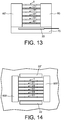
- Such a network can take different forms, with variable steps or fixed steps, as will be explained in connection with the Figures 13 to 15 .
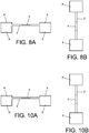
- a device comprises a plurality of nanowires 1, 21, 31, .... according to the invention, arranged parallel to each other, each of the two ends of each nanowire being connected to a pad 60, 60 'or to a part of a substrate.
- the current flowing in the wires enters through the stud 60 and leaves the stud 60 '.
- Each of these devices comprises at least one control electrode 22, 22 'parallel to the nanowires.
- the network represented in figure 13 is vertical type, that is to say perpendicular to the plane of a wafer or a substrate 70 forming a support.
- the network represented in figures 14 and 15 is of horizontal type, that is to say that the nanowires form a two-dimensional array located in the plane of a wafer or a substrate 20, and in which they may have been formed.
- References 22, 22 ' designate two control electrodes, arranged on both sides of the nanowire array, parallel to these. The current flowing in the wires enters the zone 600 and leaves the zone 600 '.
- the nanowires are of increasing lengths depending on a direction perpendicular to the nanowires. Each nanowire can then be individually addressed because each of them has a frequency different from that of the other nanowires. Each nanowire can detect different chemical species by selective functionalization. Each species will correspond to a given frequency.
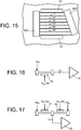
- Means for actuating a nanowire according to the invention comprise, for example, electrostatic type means.
- the actuating means may comprise means of the thermoelastic type or magnetic type or any other means. Such means make it possible to give the nanowire a movement in a direction perpendicular to its direction of extension.
- the electrostatic actuation uses the electrostatic force generated between the electrode 22 (or 22 ') and the nanowire or nanowires by applying a potential difference.
- thermoelastic actuation is usable when the two layers (metallic and insulating) are of the same length, equal to that of the nanowire. This type of operation exploits the heating effect in each of the layers.
- the layers being of different natures, the expansions are different, which generates a bending moment and therefore a movement of the nanowire.
- a device according to the invention can implement means for reading the resistance variation of the nanowire or nanowires. Examples of such means will be given in Figures 16 - 18 .
- the resistance variation across the nanowire (s) can be measured directly through the modulation of current I through it, at constant reading voltage. This is for example the case in the diagram of the figure 16 : a constant voltage V dc is applied across the nanowire.
- the reference 50 symbolizes an excitation electrode to which an AC voltage V ac is applied.
- the output signal, a current i ac is connected to an amplifier 52.
- the scheme of the figure 17 represents a direct measurement with half a bridge.
- the nanowire is under a constant voltage V dc .
- the electrodes 51 and 53 make it possible to apply to one of the parts of the wires an alternating voltage of frequency ⁇ .
- the alternating current iac that comes out, taken between the two parts of the bridge is sent to an amplifier 52.
- a heterodyning technique allows to reduce the resistance measurement from high frequencies to low frequencies. This technique is equally usable on a direct measurement as on a differential measurement by bridge. For this technique we can refer to I. Bargatin et al. "Applied Physics Letters", vol. 86, 133109 (2005) ).
- AC voltages can be generated with local oscillators.
- the reading system can be integrated (structured on the same chip) or placed on an external ASIC.
- the transduction takes place through the nanowire, which is therefore used both as a test mass (moving part) and as a gauge element to achieve the desired piezoresistive conversion.
- a device thus makes it possible to know the variation of resistance ⁇ R, related to the variation of stress ( ⁇ ) induced by the vibration of the nanowire, since ⁇ R is proportional to the stress.
- the first term (d ⁇ / ⁇ ) corresponds to the piezoresisitive effect strictly speaking, while the second term ( ⁇ L (1 + 2v)) corresponds to a purely geometrical effect.
- the second term is several orders of magnitude lower than the first.
- ⁇ ij are the elements of the piezoresistivity tensor expressed along the main crystalline axes of the semiconductor.
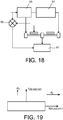
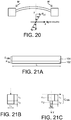
- ⁇ L and ⁇ T are respectively the longitudinal piezoresistive coefficient and the transverse piezoresistive coefficient expressed in a principal reference (N, T) of the nanowire (see figure 19 ), N being in the direction of the nanowire direction, T being in a transverse direction.
- ⁇ L and ⁇ T are respectively the longitudinal and transverse stresses applied, as illustrated on the figure 19 .
- I is the quadratic moment
- M the sagging moment represented in figure 20
- y is the ordinate, taking the neutral fiber, along which the stresses are zero (dashed line on the figure 20 ) as origin.
- the average stress on the section of the nanowire is zero.
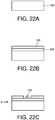
- FIG 21A of rectangular section composed of a portion 102 of slightly doped silicon, of thickness t 2 (for example doping is about 10 15 cm -3 to 10 19 cm -3 ) and a portion 104 nitride SiN of thickness t 1 piezoresistive.
- the nitrided part 104 here has a greater thickness t 1 than the silicon part 102 (thickness t 2 ) in order to concentrate the stress.
- the thickness of the Si layer becomes negligible compared to that of SiN, and the stress in the Si is then maximal and equal to the stress calculated on the outer fiber of the SiN layer.
- the Figures 21B and 21C explain how to calculate the position of this neutral fiber by considering the principle of the transformed section. Then, knowing the position of this neutral fiber and using equation (4), we can deduce the average stress in the Si.
- the stress in the Si is, as a first approximation, the stress applied to the outermost fiber of the SiN, considering that the neutral fiber is given by c 1 : ⁇
- the x M x t 1 2 I with I ⁇ I 1
- G is of the order of unity to a few units (typically 2 for metals).
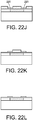
- a silicon wafer 200 is selected.
- FIG 22B two epitaxies are successively made of a SiGe layer 202 and a Si layer 204.
- the proportion of germanium in the SiGe layer 202 may be set at a given value; it can also be variable in this layer, which induces a variation of the initial stress. We can therefore adjust this initial stress by controlling the proportion of germanium.
- an actuation electrode can be structured.
- This nanobeam is then released by tunnel etching of the SiGe 204 layer, which is illustrated, according to two views, by Figures 22D and 22E .
- the view of the figure 22E is a side view along arrow A of the figure 22C .
- the section of the nanobeam is then reduced to form one or more nanowires 210 ( figures 22F and 22G , respectively from Figures 22D and 22E ), until they reach a diameter or a dimension, in a section, of the order of 25 nm or, more generally, between 10 and 30 nm.
- an oxide deposit 208 which includes the whole of the nanowire, 210, and which fills in particular the gap between the nanowire and the substrate but which is also deposited above the nanowire.
- the oxide deposit produced above the nanowires can then undergo lithography and etching operations ( figure 22I ), in order to clear nanowire access zones with a view to transforming certain selected zones.
- nitriding 220 of the unobstructed portions of the nanowire for example to a thickness of 10 nm, the technique used being an annealing technique that does not induce a reaction in the oxide.
- the oxide 208 above the wire is removed; removal of the SiN on the oxide can be carried out wet.
- the contact zones can be thickened and made metallic by doping and / or siliciding and / or metallization.
- the nanowire is released by etching the oxide 208 disposed in the cavity in contact with the substrate ( figure 22L ).
- the first two steps of this process can be removed using an SOI plate.
- an etching of the oxide is performed in place of etching of the SiGe layer.
- the Liberation ( figure 22D ) is then done by steam HF.
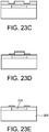
- a deposit 217 of metal (nickel or platinum) is then made on all the zones ( Figure 23B ).
- silicidation by diffusing the metal of the unobstructed portions of the nanowire, for example to a thickness of 6 nm.
- the technique used is an annealing technique that does not induce a reaction in the oxide.
- the silicidation process can be replaced by doping (until amorphization).
- the oxide 208 is removed above the nanowire; the removal of the NiSi on the oxide can be carried out wet. Finally, the nanowire is released, by etching the oxide disposed in the cavity 220 in contact with the substrate 200 ( figure 23E ).
- the first two steps can be removed using an SOI plate.
- the release is then, again, by steam HF.
- a bilayer consisting of a layer 302 of SiO2 or SiGe or Si and a layer 304 of SiGe or Si is produced ( figure 24A ).
- a layer of resin can be fo-rmée above of this bilayer and then etched to form patterns 306 which will allow etching of the layer 302 ( figure 24B ).
- An annealing optionally makes it possible to round the tops of the studs 308, 310 of Si thus produced.
- a succession of annealing and / or oxidation steps may be performed to round and reduce the section of the nanowire.
- One or more annealing and / or oxidation steps round off the nanowires, resulting in a reduction of the section of these nanowires, to a diameter of about 5 nm, for example. Recrystallization can be obtained by annealing.
- a mask 312 made of SiO 2 or SiN or bilayer is deposited and etched.
- Silicidation 320 is then carried out, as previously described, and with a selective shrinkage, respectively of nickel, platinum, cobalt, ... ( figure 24D ).
- the unprotected portions are silicided by the spacer 312.
- the measuring means can be realized by an external circuit.
- the actuation for example electrostatic, is carried out via a gap between the substrate and the nanowire after release of the nanowire. It is preferentially achieved by etching a gap "Lateral" between the nanowire and an electrode, during the etching step to define the nanowire.
- the nanowire can be vibrated by the use of actuating means comprising a lateral electrode and an electrode under the nanowire.
- a sensor according to the invention can be used as a chemical sensor (such an application with another sensor is described in Y. Wims et al. Sensors and Actuators B 108 (2005) )), in the gas phase or in the liquid phase or as molecular force sensors (such an application with another sensor is described in JL Arlett et al. Nobel Symposium, 131 (2006) )), or in the field of mass spectrometry (such an application with another sensor is described in W. Jensen et al. Nature Nanotechnology 9, 533 (2008) )).
- one or more sensitive zones can be localized, hence an improvement in the transduction efficiency.
- a first-order effect is obtained in the semiconductor, hence an increased detection effect compared to the known techniques, in particular described in the document WO 2005/106417 .
Abstract
L'invention concerne un dispositif capteur, de type à nanofil, comportant :
- une pluralité de nanofils, disposés parallèles entre eux, les nanofils étant de longueur croissante en fonction d'une direction perpendiculaire aux nanofils, chaque nanofil comportant une première zone (2), conductrice, et une deuxième zone (4), en matériau isolant, cette deuxième zone n'occupant pas toute l'épaisseur du nanofil, et un courant pouvant circuler dans ce dernier depuis l'une de ses extrémités à l'autre ;
- et deux zones (60, 60', 600, 600') de maintien fixes, auxquelles les extrémités de chaque nanofil sont fixées.

a plurality of nanowires, arranged parallel to one another, the nanowires being of increasing length as a function of a direction perpendicular to the nanowires, each nanowire comprising a first conductive zone (2) and a second zone (4) made of insulating material; this second zone does not occupy all the thickness of the nanowire, and a current can flow in the latter from one of its ends to the other;
and two fixed holding zones (60, 60 ', 600, 600') to which the ends of each nanowire are fixed.
Description
L'invention concerne la réalisation et la mise en oeuvre de capteurs à base de nanofils. Elle trouve des applications dans des domaines variés, tel que celui des capteurs chimiques notamment en phase gazeuse ou en phase liquide ou celui des capteurs de force notamment inertiel ou moléculaire ou encore dans le domaine de la spectrométrie de masse.The invention relates to the production and implementation of sensors based on nanowires. It finds applications in various fields, such as that of chemical sensors, in particular in the gas phase or in the liquid phase, or that of force sensors, particularly inertial or molecular sensors, or else in the field of mass spectrometry.
Un nanofil possède un très faible diamètre (inférieur à <100 nm), un ratio surface/volume très favorable et est donc sensible à toute perturbation externe, par exemple par modulation de leur conductance électrique lorsque des atomes sont absorbés à sa surface. Les nanofils sont donc des candidats pour la mesure ultime de masse avec des précisions attendues proches du dalton (1.67x10⁻²⁴ g).A nanowire has a very small diameter (less than <100 nm), a very favorable surface / volume ratio and is therefore sensitive to any external disturbance, for example by modulating their electrical conductance when atoms are absorbed on its surface. The nanowires are therefore candidates for the ultimate mass measurement with expected accuracies close to the dalton (1.67x10 -24 g).
Lorsqu'ils sont utilisés en tant qu'éléments mécaniques vibrants, leur sensibilité, qui est définie comme le rapport du décalage en fréquence induit par la masse ajoutée (par exemple par adsorption) à leur masse propre, est forte car cette dernière (masse propre) est très faible (1,7 ag pour un fil de 1 µm de long et un diamètre de 30 nm).When they are used as vibrating mechanical elements, their sensitivity, which is defined as the ratio of the frequency shift induced by the added mass (for example by adsorption) to their own mass, is high because the latter (own mass) ) is very low (1.7 ag for a
On connaît aussi une structure de capteur décrite dans le document
Dans le dispositif décrit dans cet article, le nanofil est à la fois le transducteur piézorésistif (le courant passe à travers le nanofil) et la masse d'épreuve (le mouvement de sa propre masse induit l'inertie).In the device described in this article, the nanowire is both the piezoresistive transducer (the current passes through the nanowire) and the test mass (the movement of its own mass induces inertia).
L'effet piézorésistif observé est la variation de la résistance du nanofil en fonction de son propre mouvement de flexion.The piezoresistive effect observed is the variation of the resistance of the nanowire as a function of its own bending movement.
Mais, dans ce type de système, l'effet piézorésistif est obtenu à l'ordre deux. C'est aussi le cas pour la structure de capteur décrite dans le document 
Un dispositif capteur selon l'invention, de type à nanofil, comporte au moins un nanofil, comportant une première zone, conductrice, et une deuxième zone, en matériau isolant, cette deuxième zone n'occupant pas toute l'épaisseur du nanofil. Un courant électrique peut circuler dans ce dernier depuis l'une de ses extrémités à l'autre.A sensor device according to the invention, of the nanowire type, comprises at least one nanowire, comprising a first conductive zone and a second zone made of insulating material, this second zone not occupying the entire thickness of the nanowire. An electric current can flow in the latter from one of its ends to the other.
La deuxième zone peut s'étendre sur une longueur inférieure à celle du nanofil.The second zone may extend over a length less than that of the nanowire.
Selon un mode de réalisation, la partie conductrice du nanofil est en matériau semiconducteur dopé, par exemple en matériau piezorésistif, ou en matériau métallique.According to one embodiment, the conductive portion of the nanowire is doped semiconductor material, for example piezoresistive material, or metal material.
Un dispositif selon l'invention permet d'exploiter un effet piézorésistif à l'ordre 1, c'est-à-dire une variation de résistance du fil, lorsqu'il est soumis à une contrainte axiale, proportionnelle à l'allongement du fil. La contrainte axiale est proportionnelle au déplacement suivant la flèche du nanofil, ce qui correspond à un déplacement en flexion.A device according to the invention makes it possible to exploit a piezoresistive effect at
La partie conductrice du nanofil peut être en un matériau semi-conducteur dopé, tel que du Si dopé. Le semi-conducteur peut être dopé avec, par exemple, de l'arsenic, ou du bore, ou du phosphore.The conductive portion of the nanowire may be of a doped semiconductor material, such as doped Si. The semiconductor may be doped with, for example, arsenic, or boron, or phosphorus.
La partie conductrice du nanofil peut être en un métal siliciuré (Si dans lequel on a diffusé du métal), par exemple en NiSi ou en WSi ou en PtSi.The conductive part of the nanowire may be a silicided metal (Si in which metal has been diffused), for example NiSi or WSi or PtSi.
Le matériau isolant peut être un matériau diélectrique ou un matériau semi-conducteur intrinsèque, par exemple du silicium ou un alliage de silicium et de Germanium (SiGe), non dopés.The insulating material may be a dielectric material or an intrinsic semiconductor material, for example undoped silicon or an alloy of silicon and Germanium (SiGe).
La zone diélectrique est par exemple en nitrure de silicium ou d'aluminium ou en oxyde de silicium.The dielectric zone is, for example, of silicon or aluminum nitride or of silicon oxide.
En variante, un dispositif selon ce mode de réalisation comporte :
- une zone diélectrique en SiGe non dopé, et une zone conductrice en Si dopé,
- ou une zone diélectrique en Si non dopé, et une zone conductrice en SiGe dopé.
- an undoped SiGe dielectric region, and a doped Si conductive zone,
- or an undoped Si dielectric region, and a doped SiGe conductive zone.
Si le silicium est dopé, il est piézorésistif et présente un facteur de jauge G élevé, par exemple d'environ 1000 alors que si le silicium est siliciuré, il devient métallique et son facteur G est très faible, par exemple d'environ 2.If the silicon is doped, it is piezoresistive and has a high G gauge factor, for example about 1000, whereas if the silicon is silicided, it becomes metallic and its G factor is very low, for example about 2.
Une extrémité du nanofil peut être fixée dans une zone de maintien, fixe, cette zone de maintien comportant en outre une zone de contact électrique. Eventuellement, chacune des deux extrémités est ainsi fixée.One end of the nanowire may be fixed in a fixed holding zone, this holding zone further comprising an electrical contact zone. Optionally, each of the two ends is thus fixed.
Au moins une zone de contact électrique peut être réalisée dans le même matériau conducteur que la première zone, conductrice, du nanofil. Une ou des zone(s) de contact peuvent être réalisées en matériau semiconducteur, plus ou moins dopé pour lui conférer des propriétés conductrices, par exemple avec un dopage compris entre 1015 cm-3 et 1019 cm-3 ou même supérieur à 1019 cm-3 ou supérieur ou égal à 1020 cm-3. (le matériau semiconducteur peut donc être dégénéré du fait de ce fort dopage). C'est par exemple un dopage avec de l'arsenic, ou, préférentiellement, du bore, ou du phosphore, éventuellement avec un gradient dans l'épaisseur. Un dispositif selon l'invention permet donc une amélioration des prises ou zones de contact ou d'accès, et donc une résistance d'accès très faible.At least one electrical contact zone may be made of the same conductive material as the first conductive zone of the nanowire. One or more zones of contact may be made of semiconductor material, more or less doped to give it conductive properties, for example with a doping of between 10 15 cm -3 and 10 19 cm -3 or even greater than 10 19 cm -3 or greater than or equal to 10 20 cm -3 . (the material semiconductor can therefore be degenerate because of this high doping). It is for example a doping with arsenic, or, preferably, boron, or phosphorus, possibly with a gradient in the thickness. A device according to the invention therefore allows an improvement of the taps or contact or access areas, and therefore a very low access resistance.
En variante, une masse mobile peut être fixée à l'une des extrémités du nanofil.Alternatively, a moving mass may be attached to one end of the nanowire.
Un dispositif selon l'invention peut comporter au moins deux nanofils, tous deux fixés à la masse mobile.A device according to the invention may comprise at least two nanowires, both fixed to the moving mass.
Selon un mode particulier de réalisation l'autre extrémité de chaque nanofil peut être fixée à une zone commune de maintien, fixe.According to a particular embodiment, the other end of each nanowire can be fixed to a common holding zone, fixed.
Un dispositif selon l'invention peut en outre comporter des moyens de transduction traduisant, en signal électrique, des mouvements d'au moins un nanofil ou d'une masse fixée à l'une des extrémités du nanofil.A device according to the invention may further comprise transduction means translating, as an electrical signal, movements of at least one nanowire or a mass attached to one end of the nanowire.
Des moyens d'actionnement d'un nanofil selon l'invention peuvent être prévus, par exemple de type électrostatique ou de type thermo-élastique ou encore de type magnétique.Means for actuating a nanowire according to the invention may be provided, for example electrostatic type or thermo-elastic type or magnetic type.
-
La
figure 1 représente une vue schématique d'un fil en flexion se déplaçant d'une amplitude a,Thefigure 1 represents a schematic view of a bending wire moving of an amplitude a , -
la
figure 2 représente un nanofil selon l'invention,thefigure 2 represents a nanowire according to the invention, -
la
figure 3 , et lesfigures 4A - 8B , représentent divers structures de nanofil selon l'invention,thefigure 3 , and theFigures 4A - 8B , represent various structures of nanowire according to the invention, -
les
figures 9A à 9C représentent un dispositif comportant plusieurs nanofil selon l'invention, disposés autour d'une masse vibrante hors de son plan,theFigures 9A to 9C represent a device comprising several nanowires according to the invention, arranged around a vibrating mass outside its plane, -
les
figures 10A et 10B représentent un nanofil métallique selon l'invention, avec une zone isolante en son centre,theFigures 10A and 10B represent a metallic nanowire according to the invention, with an insulating zone at its center, -
les
figures 11A et 11B représentent un nanofil métallique selon l'invention, avec une couche isolante proche des encastrements,theFigures 11A and 11B represent a metallic nanowire according to the invention, with an insulating layer close to the recesses, -
les
figures 12A et 12B représentent un dispositif comportant deux nanofils selon l'invention, disposés de manière à réaliser deux bras de flexion attachés à une masse vibrante hors de son plan,theFigures 12A and 12B represent a device comprising two nanowires according to the invention, arranged so as to produce two bending arms attached to a vibrating mass outside its plane, -
les
figures 13 - 15 représentent des dispositifs à réseaux de nanofils selon l'invention,theFigures 13 - 15 represent devices with nanowire networks according to the invention, -
les
figures 16 - 18 représentent des moyens pour mesurer une variation de résistance dans un nanofil selon l'invention,theFigures 16 - 18 represent means for measuring a variation of resistance in a nanowire according to the invention, -
la
figure 19 est un schéma d'une jauge piézorésistive avec les axes principaux (N, T) associés,thefigure 19 is a diagram of a piezoresistive gauge with associated principal axes (N, T), -
la
figure 20 est un schéma représentant un moment fléchissant et une contrainte axiale induite dans une section d'un nanofil,thefigure 20 is a diagram representing a bending moment and an axial stress induced in a section of a nanowire, -
les
figures 21A - 21C représentent un nanofil selon l'invention, et le calcul de la position de la fibre neutre c à partir des positions des fibres neutres des sections de chaque couche,theFigures 21A - 21C represent a nanowire according to the invention, and the calculation of the position of the neutral fiber c from the positions of the neutral fibers of the sections of each layer, -
les
figures 22A à 22L et23A - 23E sont des étapes de réalisation de différents dispositifs selon l'invention,theFigures 22A to 22L and23A - 23E are steps for producing different devices according to the invention, -
les
figures 24A à 24E sont d'autres étapes de réalisation d'un dispositif selon l'invention.theFigures 24A to 24E are other steps of realization of a device according to the invention.
Une structure de dispositif selon l'invention est illustrée en
Deux types de zone conductrice 2, et donc deux types de transductions, peuvent être exploitées. On va donc successivement décrire ces deux modes de réalisation.Two types of conducting
Dans un premier mode de réalisation de l'invention, l'une de ces zones, ici la zone 2, est piezorésistive et conductrice, tandis que la zone 4 est isolante ou diélectrique. Ce premier type de dispositif selon l'invention met donc en oeuvre la piézorésistivité intrinsèque à un nanofil qui est par exemple constitué d'un matériau semi conducteur dopé. Le facteur de jauge G (longitudinal) est alors élevé, de l'ordre de 1000, ou plus.In a first embodiment of the invention, one of these zones, here
La zone conductrice 2 est par exemple réalisée en un matériau semi-conducteur, tel que du silicium (mais d'autres semi-conducteurs peuvent être utilisés), qui peut être plus ou moins dopé pour lui conférer des propriétés conductrices.The
Le dopage peut-être plus ou moins important, par exemple compris entre 1015 cm-3 et 1019 cm-3. C'est par exemple un dopage avec de l'arsenic, ou, préférentiellement, du bore, ou du phosphore, éventuellement avec un gradient dans l'épaisseur. Un tel dopage peut être réalisé lors de l'épitaxie d'une couche de matériau semi-conducteur dans laquelle le nanofil sera réalisé. En variante, il peut être réalisé par d'autres techniques, par implantation par exemple.Doping may be more or less important, for example between 10 15 cm -3 and 10 19 cm -3 . It is by for example doping with arsenic, or, preferably, boron or phosphorus, optionally with a gradient in the thickness. Such doping can be achieved during the epitaxy of a layer of semiconductor material in which the nanowire will be made. Alternatively, it can be achieved by other techniques, for example implantation.
La zone isolante 4 peut, quant à elle, être en un nitrure ou en un oxyde, par exemple elle est en SiN, ou en un oxyde, par exemple en Si02. Avantageusement, la couche isolante est en AlN. En variante, c'est une pluralité de couches simples diélectriques.The insulating
En variante, une couche peut être graduellement modifiée, par exemple par un gradient de dopage dans l'épaisseur, par implantation en une fois ou par une succession d'étapes d'implantation. Ce gradient peut être réalisé par exemple par une implantation suivie d'un recuit. On peut réaliser également une implantation utilisant des étapes successives d'implantation à des profondeurs différentes de pénétration.As a variant, a layer may be gradually modified, for example by a doping gradient in the thickness, by implantation at one time or by a succession of implantation steps. This gradient can be achieved for example by implantation followed by annealing. Implantation can also be performed using successive implantation steps at different depths of penetration.
Ces exemples de matériaux diélectriques et de matériaux piézorésistifs conducteurs peuvent être employés dans les divers exemples ci-dessous du premier mode de réalisation selon l'invention.These examples of dielectric materials and conductive piezoresistive materials may be employed in the various examples below of the first embodiment of the invention.
Dans un autre mode de réalisation, l'une de ces zones, ici la zone 2, est métallique tandis que la zone 4 est isolante ou diélectrique. On favorise ainsi une transduction dite « piézorésistive » due à l'allongement du métal, à faible facteur de jauge (longitudinal). Les nanofils métalliques sont beaucoup moins résistifs que ceux en matériau semi-conducteur. Le bruit de Johnson associé est donc plus faible et permet d'atteindre des résolutions plus faibles que dans le premier mode de réalisation. En contre partie, la sensibilité (pente de la réponse) est plus faible que dans le cas piézorésisitif obtenu avec un semi-conducteur.In another embodiment, one of these zones, here
Un nanofil de ce deuxième mode de réalisation peut être réalisé par exemple à partir d'un fil en un siliciure tel que NiSi, ou WSi2, ou PtSi. Il est éventuellement possible de doper par implantation jusqu'à l'amorphisation un nanofil en matériau semi-conducteur ou de réaliser un dopage pendant une épitaxie d'une couche dans laquelle le nanofil sera créé (cette solution permet de générer un gradient de dopage).A nanowire of this second embodiment can be made for example from a wire into a silicide such as NiSi, or WSi2, or PtSi. It is optionally possible to dope by implantation until amorphization a nanowire semiconductor material or to perform a doping during an epitaxy of a layer in which the nanowire will be created (this solution can generate a doping gradient) .
Un matériau isolant pour la zone 4 de ce deuxième mode de réalisation est par exemple le silicium intrinsèque, ou un isolant tel que SiN ou SiO2.An insulating material for
Là encore, ces exemples de matériaux diélectriques et de matériaux piézorésistifs conducteurs peuvent être employés dans les divers exemples ci-dessous du deuxième mode de réalisation selon l'invention.Again, these examples of dielectric materials and conductive piezoresistive materials may be employed in the various examples below of the second embodiment of the invention.
Quel que soit le mode de réalisation envisagé, un dispositif selon l'invention met en oeuvre la circulation d'un courant i sur toute la longueur du nanofil. Or, la résistance de la portion conductrice varie en fonction de sa déformation. Le nanofil est donc utilisé à la fois comme masse d'épreuve (il constitue la partie mobile) et comme élément de jauge (ce sont ses propriétés électriques que l'on mesure). On peut en particulier mesurer la variation de courant i dans le nanofil, celui-ci étant sous tension constante, lorsque ce nanofil est soumis à une déformation.Whatever the embodiment envisaged, a device according to the invention implements the circulation of a current i over the entire length of the nanowire. However, the resistance of the conductive portion varies as a function of its deformation. The nanowire is therefore used both as a proof mass (it constitutes the mobile part) and as a gauge element (it is its electrical properties that are measured). In particular, it is possible to measure the variation of current i in the nanowire, the latter being under constant tension, when the nanowire is subjected to deformation.
Sur la
L'épaisseur ou le diamètre en est inférieur à 50 nm, ou à quelques dizaines de nm, elle ou il est par exemple de 40 nm. Dans un nanofil selon l'invention, on a en outre au moins la condition suivante (C1) : ed < en. Autrement dit, la zone diélectrique n'occupe pas toute l'épaisseur du nanofil, et un courant i peut circuler dans ce dernier depuis l'une de ses extrémités E1 à l'autre extrémité E2. ed est par exemple égal à 10 nm. Pour un effet optimal, on considère par exemple une épaisseur d'isolant de 40 nm et une épaisseur de Si dopé de 10 nm, ou plus généralement une épaisseur d'isolant supérieure à celle du Si dopé ; encore selon un autre exemple, on considère une épaisseur de Si de 40 nm et une épaisseur de métal de 10 nm, ou plus généralement une épaisseur de Si supérieure à celle du métal.The thickness or the diameter e n is less than 50 nm, or a few tens of nm, or it is for example 40 nm. In a nanowire according to the invention, there is further at least the following condition (C1): e d <e n . In other words, the dielectric zone does not occupy the entire thickness of the nanowire, and a current i can flow in the latter from one of its ends E 1 to the other end E 2 . e d is for example equal to 10 nm. For an optimal effect, consider for example an insulation thickness of 40 nm and a doped Si thickness of 10 nm, or more generally an insulation thickness greater than that of the doped Si; again according to another example, a Si thickness of 40 nm and a metal thickness of 10 nm, or more generally a thickness of Si greater than that of the metal, are considered.
S'il y a plusieurs zones diélectriques 4 le long du fil, chacune respecte cette condition C1. Dans certains modes de réalisation, on a en outre la condition (C2) suivante : ld < Ln, ce qui signifie que la zone diélectrique 4 n'a pas une extension longitudinale suivant toute la longueur Ln du nanofil.If there are several
La zone 4, isolante ou diélectrique, peut donc être localisée dans le nanofil. Cette localisation permet en particulier de minimiser la résistance globale du fil, afin d'optimiser le rapport signal à bruit : pour un matériau isolant donné, on peut sélectionner les dimensions ld et ed de la zone 4 pour adapter la résistance du fil.The
La
Dans l'exemple de la
Les
La variante des
Cette variante est plus avantageuse que la précédente car les contraintes appliquées au fil sont maximales à ses extrémités, proches des zones d'encastrement 6, 6'. Le signal électrique est donc d'autant plus fort dans ce type de structure.This variant is more advantageous than the previous one since the stresses applied to the wire are maximum at its ends, close to the embedding
Afin de diminuer la valeur de la résistance des contacts 6, 6', il est possible de siliciurer et/ou doper les ancrages et éventuellement les zones de nanofils proches des ancrages qui contribuent alors aux contacts. Il est également possible d'alterner les couches. Ainsi sont représentés :
- en
figures 6A, 6B ,un nanofil 1 en silicium ayant en son centre unecouche 4 de diélectrique qui satisfait aux deux conditions C1 et C2 ci dessus. On voit sur cet exemple que le nanofil comporte uneportion centrale 2 en matériau piézorésistif et unezone 4 diélectrique. Les portions latérales 12, 12' du fil sont réalisées par exemple en un siliciure, tel que du NiSi ; elles forment des prolongements de chacune des zones conductrices 8, 8'. Autrement dit, ces dernières débordent de chaque plot pour former une partie du nanofil 1. Cette configuration permet d'améliorer fortement les contacts ohmiques entre les extrémités du fil et chacune des zones conductrices 8, 8' ; plus généralement, et comme déjà indiqué, une ou des zone(s) de contact peuvent être réalisées en matériau semiconducteur, plus ou moins dopé pour lui conférer des propriétés conductrices, par exemple avec un dopage compris entre 1015 cm-3 et 1019 cm-3 ou même supérieur à 1019 cm-3 ou supérieur ou égal à 1020 cm-3. (le matériau semiconducteur peut donc être dégénéré du fait de ce fort dopage). C'est par exemple un dopage avec de l'arsenic, ou, préférentiellement, du bore, ou du phosphore, éventuellement avec un gradient dans l'épaisseur. Un dispositif selon l'invention permet donc une amélioration des prises ou zones de contact ou d'accès, et donc une résistance d'accès très faible,
- en
figures 7A, 7B , un nanofil en silicium 2 dopé avec une couche 4 de SiGe non dopée, à comportement isolant car présentant une très forte résistivité (cas du SiGe non dopé (intrinsèque) de haute résistivité, ou SiGe « HR »). Une telle couche 4 en SiGe peut être obtenue par exemple par épitaxie. Cette couche 4 a une longueur identique à celle du nanofil, mais son épaisseur est inférieure à celle du nanofil, conformément à la condition C1 indiquée ci-dessus, - en
figures 8A, 8B , un nanofil en silicium 2 (ou en un autre matériau semi-conducteur dopé) avec une couche 4 de SiGe non dopée et localisée (au centre du nanofil dans l'exemple). Une telle couche 4 en SiGe peut être obtenue par exemple par épitaxie. Cette fois, cette couche 4 a une longueur inférieure à celle du nanofil, conformément à la condition C2 indiquée ci-dessus et son épaisseur est inférieure à celle du nanofil, conformément à la condition C1 indiquée ci-dessus.
- in
Figures 6A, 6B , asilicon nanowire 1 having at its center adielectric layer 4 which satisfies the two conditions C1 and C2 above. It can be seen in this example that the nanowire comprises acentral portion 2 of piezoresistive material and adielectric zone 4. Thelateral portions 12, 12 'of the wire are made for example of a silicide, such as NiSi; they form extensions of each of theconductive zones 8, 8 '. In other words, the latter protrude from each pad to form part of thenanowire 1. This configuration makes it possible to greatly improve the ohmic contacts between the ends of the wire and each of theconductive zones 8, 8 '; more generally, and as already indicated, one or more contact zones may be made of semiconductor material, more or less doped to give it conductive properties, for example with a doping between 10 15 cm -3 and 10 19 cm -3 or even greater than 10 19 cm -3 or greater than or equal to 10 20 cm -3 . (The semiconductor material can therefore be degenerated because of this high doping). It is for example a doping with arsenic, or, preferably, boron, or phosphorus, possibly with a gradient in the thickness. A device according to the invention therefore allows an improvement of the taps or contact or access areas, and therefore a very low access resistance,
- in
Figures 7A, 7B , a silicon-dopednanowire 2 with alayer 4 of undoped SiGe, with insulating behavior because it has a very high resistivity (case of undoped (intrinsic) SiGe of high resistivity, or SiGe "HR"). Such aSiGe layer 4 can be obtained for example by epitaxy. Thislayer 4 has a length identical to that of the nanowire, but its thickness is less than that of the nanowire, according to the condition C1 indicated above, - in
Figures 8A, 8B , asilicon 2 nanowire (or other doped semiconductor material) with alayer 4 of undoped and localized SiGe (in the center of the nanowire in the example). Such aSiGe layer 4 can be obtained for example by epitaxy. This time, thislayer 4 has a length less than that of the nanowire, in accordance with the condition C2 indicated above and its thickness is less than that of the nanowire, in accordance with the condition C1 indicated above.
Dans le cas des
Une structure de nanofil selon l'invention, selon les
Les
Cette structure comporte une partie centrale 30, formant une masse vibrante hors de son plan. Dans cet exemple, elle est, en vue de dessus, de forme sensiblement rectangulaire reliée à chacune des deux zones d'encastrement 6, 6' par deux bras 33, 33', 35, 35' .This structure comprises a
D'autres formes en vue de dessus sont possibles, par exemple circulaire ou elliptique, là encore avec des bras.Other shapes in top view are possible, for example circular or elliptical, again with arms.
Chaque bras est en fait constitué d'un nanofil selon la présente invention. Une extrémité de chaque nanofil est reliée à la partie fixe 6, 6' du dispositif, par des zones conductrices 8, 8', 18, 18', comme dans les exemples précédents.Each arm is in fact made of a nanowire according to the present invention. One end of each nanowire is connected to the
La masse 30 contient elle-même une portion diélectrique 34, sur toute l'épaisseur de la masse, et qui sépare le dispositif en deux parties 30', 30", chacune de ces parties formant une zone de mesure avec les deux nanofils 33, 33' et 35, 35' qui lui sont reliés. Le reste de la masse 30 est en matériau conducteur. On voit sur la
Plus généralement, un ou plusieurs nanofils peuvent être associés ou reliés à une ou des masses par exemple selon un réseau. Cela permet d'augmenter la surface de capture pour des applications de mesure de masse ou d'augmenter la masse inertielle dans le cas de capteur de force inertiel.More generally, one or more nanowires can be associated or connected to one or more masses, for example according to a network. This makes it possible to increase the capture surface for mass measurement applications or to increase the inertial mass in the case of an inertial force sensor.
Dans un nanofil selon l'invention, des contraintes internes peuvent apparaître, du fait de différences entre les paramètres de mailles du conducteur 2 et du diélectrique 4 et du fait de la différence entre les coefficients de dilation thermique de chacun de ces matériaux. Ces contraintes peuvent être contrôlées, afin d'obtenir des nanofils en tension. Ce contrôle peut être réalisé par exemple en contrôlant la ou les températures de dépôt, et en maîtrisant les épaisseurs relatives de différentes couches. Un nanofil selon l'invention peut donc offrir une rigidité plus élevée et une fréquence de résonance plus élevée qu'un nanofil réalisé uniquement en silicium. Ceci s'applique de manière générale, à un dispositif quelconque selon l'invention.In a nanowire according to the invention, internal stresses may arise, due to differences between the mesh parameters of the
Le second type de dispositif selon l'invention met en oeuvre un matériau 2 métallique, de préférence à faible facteur de jauge G (environ 2).The second type of device according to the invention uses a
En
La variante des
La structure d'un dispositif selon l'invention peut être plus complexe. Elle peut avoir la forme de celle qui serait obtenue selon les
D'autres structures mettant en oeuvre un dispositif avec nanofil dissymétrique selon l'invention peuvent être réalisées, qu'il s'agisse de nanofils selon l'un quelconque des modes de réalisation présentés ci-dessus.Other structures implementing a device with asymmetrical nanowire according to the invention can be realized, whether they are nanowires according to any one of the embodiments presented above.
C'est par exemple le cas de la structure des
On peut mettre en réseau des dispositifs selon l'invention qui ont été décrits plus haut.Devices according to the invention which have been described above can be networked.
Un tel réseau peut prendre différentes formes, à pas variables ou à pas fixes, comme ceci va être expliqué en liaison avec les
Sur chacune de ces figures, un dispositif comporte une pluralité de nanofils 1, 21, 31,.... selon l'invention, disposés parallèles entre eux, chacune des deux extrémités de chaque nanofil étant reliée à un plot 60, 60' ou à une partie d'un substrat. Le courant circulant dans les fils entre par le plot 60 et ressort par le plot 60'.In each of these figures, a device comprises a plurality of
Chacun de ces dispositifs comporte au moins une électrode de contrôle 22, 22' parallèle aux nanofils.Each of these devices comprises at least one
Le réseau représenté en
Le réseau représenté en
Dans la variante du réseau représenté en
Des moyens d'actionnement d'un nanofil selon l'invention comportent par exemple des moyens de type électrostatique. En variante, les moyens d'actionnement peuvent comporter des moyens de type thermoélastique ou de type magnétique ou tout autre moyen. De tels moyens permettent de donner au nanofil un mouvement suivant une direction perpendiculaire à sa direction d'extension.Means for actuating a nanowire according to the invention comprise, for example, electrostatic type means. Alternatively, the actuating means may comprise means of the thermoelastic type or magnetic type or any other means. Such means make it possible to give the nanowire a movement in a direction perpendicular to its direction of extension.
L'actionnement électrostatique utilise la force électrostatique générée entre l'électrode 22 (ou 22') et le ou les nanofils par application d'une différence de potentiel.The electrostatic actuation uses the electrostatic force generated between the electrode 22 (or 22 ') and the nanowire or nanowires by applying a potential difference.
L'actionnement thermoélastique est utilisable quand les deux couches (métallique et isolante) sont de même longueur, égale à celle du nanofil. Ce type d'actionnement exploite l'effet d'échauffement dans chacune des couches. Les couches étant de natures différentes, les dilatations sont différentes, ce qui génère un moment de flexion et donc un mouvement du nanofil.The thermoelastic actuation is usable when the two layers (metallic and insulating) are of the same length, equal to that of the nanowire. This type of operation exploits the heating effect in each of the layers. The layers being of different natures, the expansions are different, which generates a bending moment and therefore a movement of the nanowire.
Un dispositif selon l'invention peut mettre en oeuvre des moyens de lecture de la variation de résistance du ou des nanofils. Des exemples de tels moyens vont être donnés en
La variation de résistance aux bornes du (ou des) nanofil(s) peut être mesurée directement à travers la modulation du courant I qui le traverse, à tension de lecture constante. C'est par exemple le cas dans le schéma de la
Le schéma de la
Une technique d'hétérodynage, représentée schématiquement en
Dans ces montages, les tensions alternatives peuvent être générées avec des oscillateurs locaux. Le système de lecture peut être intégré (structuré sur la même puce) ou placé sur un ASIC externe.In these setups, AC voltages can be generated with local oscillators. The reading system can be integrated (structured on the same chip) or placed on an external ASIC.
Dans un dispositif selon l'invention, La transduction (la création d'un courant par le mouvement du nanofil) s'effectue à travers le nanofil, celui-ci est donc utilisé à la fois comme masse d'épreuve (partie mobile) et comme élément de jauge pour réaliser la conversion piézorésistive souhaitée.In a device according to the invention, the transduction (the creation of a current by the movement of the nanowire) takes place through the nanowire, which is therefore used both as a test mass (moving part) and as a gauge element to achieve the desired piezoresistive conversion.
On montre que la variation relative de la résistance du nanofil devient alors proportionnelle à l'amplitude du mouvement ; en reprenant les notations de l'équation (1) : 
Un dispositif selon l'invention permet donc de connaître la variation de résistance ΔR, liée à la variation de contrainte (σ) induite par la vibration du nanofil, car ΔR est proportionnelle à la contrainte.A device according to the invention thus makes it possible to know the variation of resistance ΔR, related to the variation of stress (σ) induced by the vibration of the nanowire, since ΔR is proportional to the stress.
D'une manière générale, une résistance formée par une structure, en forme de nanofil, ayant à la fois des propriétés conductrices et des propriétés élastiques, varie en fonction d'une contrainte axiale comme suit : 
Le premier terme (dρ/ρ) correspond à l'effet piézorésisitif à proprement parler, alors que le second (εL (1+2v)) correspond à un effet purement géométrique.The first term (dρ / ρ) corresponds to the piezoresisitive effect strictly speaking, while the second term (ε L (1 + 2v)) corresponds to a purely geometrical effect.
Dans le cas d'un semi-conducteur comme le silicium, le second terme est de plusieurs ordres de grandeur inférieur au premier.In the case of a semiconductor such as silicon, the second term is several orders of magnitude lower than the first.
La piézorésistivité est un phénomène physique qui relie une variation relative de résistivité ![]()

![]()
![]()
![]()
![]()
![]()
Πij sont les éléments du tenseur de piézorésistivité exprimés selon les axes cristallins principaux du semi-conducteur. ΠL et ΠT sont respectivement le coefficient piézorésistif longitudinal et le coefficient piézorésistif transversal exprimés dans un repère principal (N, T) du nanofil (voir
Dans le cas d'un nanofil orienté selon l'axe <110>, la variation de résistance se réduit à : ![]()
![]()
On prend d'abord le cas d'un nanofil homogène. Ce cas peut être traité comme une poutre de section circulaire. Ce fil est soumis à une contrainte, du fait de son passage à une position, illustré en 
I est le moment quadratique, M le moment fléchissant représenté en
La contrainte moyenne sur la section du nanofil est nulle.The average stress on the section of the nanowire is zero.
On prend maintenant le cas d'un nanofil non homogène, comme illustré en
La partie nitrurée 104 a ici une épaisseur t1 plus importante que la partie 102 en silicium (épaisseur t2) afin de concentrer la contrainte. En cas limite, l'épaisseur de la couche de Si devient négligeable devant celle de SiN, et la contrainte dans le Si est alors maximale et égale à la contrainte calculée sur la fibre externe de la couche SiN. Dans un cas plus général (t2 non négligeable devant t1), on détermine la position de la fibre neutre. Celle-ci dépend non seulement des épaisseurs mais aussi des modules d'Young respectifs (ESi=160 GPa selon <110> et ESiN=230 GPa) .The
Les
La section transformée est définie par : ![]()
![]()
![]()
![]()
Avec c1= t1/2 et C2= t2/2.With c 1 = t 1/2 and C 2 = t 2/2.
Le moment quadratique de la structure équivalente est donné par l'expression suivante : 
Finalement, la contrainte moyenne dans une section en x (coordonnée longitudinale) de Si est : 
Lorsque l'épaisseur du silicium est négligeable devant celle du SiN (cas favorable) la contrainte dans le Si est en première approximation la contrainte appliquée sur la fibre la plus externe du SiN, en considérant que la fibre neutre est donnée par c1 : 
Pour obtenir la contrainte moyenne le long de la partie Si constituant le fil, il faut intégrer (6) ou (7) sur la longueur de le fil en considérant la déformée.To obtain the average stress along the part Si constituting the wire, it is necessary to integrate (6) or (7) along the length of the wire by considering the deformed.
En sachant que : 
En considérant une jauge de dimension z, l'expression (7) se réduit à : 
Finalement, la variation de résistance s'exprime comme suit : 
Dans le cas du second mode de réalisation selon l'invention, on exploite directement l'élongation de la structure. L'origine de la variation est différente mais le calcul est identique : ![]()
![]()
G est de l'ordre de l'unité à quelques unités (typiquement 2 pour les métaux).G is of the order of unity to a few units (typically 2 for metals).
On voit que, dans les deux cas, la variation de résistivité est à l'ordre 1.It can be seen that in both cases the resistivity variation is in the
Dans un nanofil selon l'invention, quel que soit le mode de réalisation considéré, la dissymétrie créée du fait des différentes conductivités électriques permet de générer des contraintes différentes au-dessus et au-dessous de la fibre neutre. Ces contraintes ne s'équilibrent pas et ce déséquilibre permet d'obtenir une mesure au premier ordre.In a nanowire according to the invention, whatever the embodiment considered, the dissymmetry created due to the different electrical conductivities makes it possible to generate different stresses above and below the neutral fiber. These constraints do not balance out and this imbalance makes it possible to obtain a first-order measurement.
On va maintenant décrire des procédés de réalisation de dispositifs selon invention.Methods for producing devices according to the invention will now be described.
Une réalisation de fils présentant des matériaux différents selon l'épaisseur est décrite dans le document
On va d'abord décrire l'enchaînement des étapes des
Dans une première étape, une plaquette de silicium 200 est sélectionnée.In a first step, a
Puis (
On procède ensuite (
Dans ce mode de réalisation on peut structurer une électrode d'actionnement.In this embodiment, an actuation electrode can be structured.
On libère ensuite cette nanopoutre par gravure tunnel de la couche de SiGe 204, ce qui est illustré, selon deux vues, en
On procède ensuite à une réduction de la section de la nanopoutre pour former un ou des nanofils 210 (
Il est ensuite procédé (
Le dépôt d'oxyde réalisé au-dessus du nanofils peut ensuite subir des opérations de lithographie et de gravure (
On peut alors procéder (
Puis (
Enfin, le nanofil est libéré, par gravure de l'oxyde 208 disposé dans la cavité en contact avec le substrat (
Les deux premières étapes de ce procédé peuvent être supprimées en utilisant une plaque SOI. Dans ce cas on réalise une gravure de l'oxyde à la place de la gravure de la couche SiGe. La libération (
On décrit maintenant l'enchaînement des étapes des
Les figures du début du procédé sont identiques aux
On part donc d'une structure telle que celle de la
On réalise ensuite un dépôt 217 de métal (nickel ou platine) sur l'ensemble des zones (
On peut alors procéder (
Puis (
Là encore, les deux premières étapes peuvent être supprimées en utilisant une plaque SOI. La libération se fait alors, là aussi, par voie HF vapeur.Again, the first two steps can be removed using an SOI plate. The release is then, again, by steam HF.
Un autre exemple de réalisation d'un procédé pour réaliser un dispositif selon l'invention va être donné, en liaison avec les
Dans une première étape, une bicouche constituée d'une couche 302 de SiO2 ou de SiGe ou de Si et d'une couche 304 de SiGe ou de Si est réalisée (
Un recuit permet éventuellement d'arrondir les sommets des plots 308, 310 de Si ainsi réalisés. En variante, une succession d'étapes de recuit et/ou d'oxydation peuvent être réalisées afin d'arrondir et de réduire la section du nanofil. Une ou plusieurs étapes de recuit et/ou d'oxydation permet d'arrondir les nanofils, d'où une réduction de la section de ces nanofils, à un diamètre d'environ 5 nm par exemple. Une recristallisation peut être obtenue par recuit.An annealing optionally makes it possible to round the tops of the
On réalise ensuite un dépôt et une gravure d'un masque 312 (espaceur) en SiO2 ou en SiN ou bicouche.Next, a mask 312 (spacer) made of
On procède ensuite à une siliciuration 320, comme décrit précédemment et à un retrait sélectif, respectivement du nickel, du platine, du cobalt,... (
Enfin (
Dans un dispositif selon l'invention, les moyens de mesure peuvent être réalisés par un circuit externe.In a device according to the invention, the measuring means can be realized by an external circuit.
L'actionnement, par exemple électrostatique, est réalisé par l'intermédiaire d'un gap entre le substrat et le nanofil après libération du nanofil. Il est préférentiellement réalisé en gravant un gap « latéral » entre le nanofil et une électrode, pendant l'étape de gravure pour définir la nanofil.The actuation, for example electrostatic, is carried out via a gap between the substrate and the nanowire after release of the nanowire. It is preferentially achieved by etching a gap "Lateral" between the nanowire and an electrode, during the etching step to define the nanowire.
Selon une variante de réalisation, le nanofil peut être mis en vibration par l'utilisation de moyens d'actionnement comportant une électrode latérale et une électrode sous le nanofil.According to an alternative embodiment, the nanowire can be vibrated by the use of actuating means comprising a lateral electrode and an electrode under the nanowire.
Un capteur selon l'invention peut être utilisé en tant que capteur chimique (une telle application avec un autre capteur est décrite dans
L'invention permet notamment de réaliser un capteur à base de nanofil avec au moins deux parties ou zones de conductivités très différentes, selon au moins deux approches :
- soit un nanofil métal/semi-conducteur par exemple obtenu par un procédé de microélectronique pour obtenir la couche conductrice et par une ou plusieurs des étapes décrites ci-dessus (par Siliciuration d'une partie du nanofil (peu ou pas dopé) ou par dopage (allant jusqu'à l'amorphisation éventuellement) d'une partie du fil),
- soit par nitruration d'au moins une partie d'un fil dopé.
- or a metal / semiconductor nanowire for example obtained by a microelectronic method to obtain the conductive layer and by one or more of the steps described above (by siliciding of a part of the nanowire (little or no doping) or by doping (up to the possible amorphization) of a part of the wire),
- or by nitriding at least a portion of a doped yarn.
En outre une ou des zones sensibles (telles que la ou les jauges piézorésistives) peuvent être localisées, d'où une amélioration de l'efficacité de transduction.In addition, one or more sensitive zones (such as the piezoresistive gauge or gauges) can be localized, hence an improvement in the transduction efficiency.
Dans tous les cas, il est possible de réaliser une amélioration de la prise de contact, du fait d'une résistance d'accès très faible, notamment par dopage de zones de contact.In all cases, it is possible to achieve an improvement in the contact, because of a very low access resistance, particularly by doping contact areas.
Dans un dispositif selon l'invention, on obtient un effet du premier ordre dans le semi-conducteur, d'où un effet de détection accru par rapport aux techniques connues, notamment décrites dans le document
Claims (9)
Applications Claiming Priority (2)
| Application Number | Priority Date | Filing Date | Title |
|---|---|---|---|
| FR0951251A FR2942660B1 (en) | 2009-02-27 | 2009-02-27 | SENSOR DEVICE BASED ON NANOWLAS |
| EP10154557.2A EP2223887B1 (en) | 2009-02-27 | 2010-02-24 | Sensor using nanowires |
Related Parent Applications (2)
| Application Number | Title | Priority Date | Filing Date |
|---|---|---|---|
| EP10154557.2A Division EP2223887B1 (en) | 2009-02-27 | 2010-02-24 | Sensor using nanowires |
| EP10154557.2A Division-Into EP2223887B1 (en) | 2009-02-27 | 2010-02-24 | Sensor using nanowires |
Publications (2)
| Publication Number | Publication Date |
|---|---|
| EP3424875A1 true EP3424875A1 (en) | 2019-01-09 |
| EP3424875B1 EP3424875B1 (en) | 2020-04-15 |
Family
ID=41465391
Family Applications (3)
| Application Number | Title | Priority Date | Filing Date |
|---|---|---|---|
| EP18187837.2A Active EP3424874B1 (en) | 2009-02-27 | 2010-02-24 | Sensor device based on nanowires with mobile mass |
| EP10154557.2A Active EP2223887B1 (en) | 2009-02-27 | 2010-02-24 | Sensor using nanowires |
| EP18187843.0A Active EP3424875B1 (en) | 2009-02-27 | 2010-02-24 | Sensor device based on nanowires of increasing length |
Family Applications Before (2)
| Application Number | Title | Priority Date | Filing Date |
|---|---|---|---|
| EP18187837.2A Active EP3424874B1 (en) | 2009-02-27 | 2010-02-24 | Sensor device based on nanowires with mobile mass |
| EP10154557.2A Active EP2223887B1 (en) | 2009-02-27 | 2010-02-24 | Sensor using nanowires |
Country Status (4)
| Country | Link |
|---|---|
| US (1) | US9382108B2 (en) |
| EP (3) | EP3424874B1 (en) |
| JP (1) | JP2010204098A (en) |
| FR (1) | FR2942660B1 (en) |
Families Citing this family (8)
| Publication number | Priority date | Publication date | Assignee | Title |
|---|---|---|---|---|
| FR2923646A1 (en) * | 2007-11-09 | 2009-05-15 | Commissariat Energie Atomique | MEMORY CELL SRAM WITH TRANSISTORS WITH VERTICAL MULTI-CHANNEL STRUCTURE |
| FR2995691B1 (en) * | 2012-09-19 | 2014-10-10 | Commissariat Energie Atomique | THERMAL FLOW SENSOR, GAS SENSOR COMPRISING AT LEAST ONE SUCH SENSOR AND PIRANI GAUGE COMPRISING AT LEAST ONE SUCH SENSOR |
| JP5990664B2 (en) * | 2013-04-19 | 2016-09-14 | コチ・ウニヴェルシテシKoc Universitesi | Nanomechanical resonator array and manufacturing method thereof |
| FR3017463B1 (en) * | 2014-02-13 | 2020-11-13 | Commissariat Energie Atomique | SUSPENDED-STRUCTURE GAS CONCENTRATION SENSOR |
| WO2017170748A1 (en) * | 2016-03-31 | 2017-10-05 | 京セラ株式会社 | Stress sensor |
| KR101919344B1 (en) | 2016-12-26 | 2018-11-20 | 한양대학교 에리카산학협력단 | METHOD FOR FABRICATING ZnO HUMIDITY SENSOR DEVICE |
| FR3086386B1 (en) * | 2018-09-21 | 2020-12-04 | Commissariat Energie Atomique | MEASURING DEVICE CONTAINING A SUSPENDED SEMICONDUCTOR WIRE |
| FR3110284B1 (en) * | 2020-05-14 | 2023-01-13 | Commissariat Energie Atomique | Detection device using piezoresistive transduction |
Citations (3)
| Publication number | Priority date | Publication date | Assignee | Title |
|---|---|---|---|---|
| WO2002080360A1 (en) * | 2001-03-30 | 2002-10-10 | California Institute Of Technology | Pattern-aligned carbon nanotube growth and tunable resonator apparatus |
| US20040112964A1 (en) * | 2002-09-30 | 2004-06-17 | Nanosys, Inc. | Applications of nano-enabled large area macroelectronic substrates incorporating nanowires and nanowire composites |
| US20080314149A1 (en) * | 2007-06-25 | 2008-12-25 | Micron Technology, Inc. | Sensor and transducer devices comprising carbon nanotubes, methods of making and using the same |
Family Cites Families (4)
| Publication number | Priority date | Publication date | Assignee | Title |
|---|---|---|---|---|
| US7302856B2 (en) * | 2003-05-07 | 2007-12-04 | California Institute Of Technology | Strain sensors based on nanowire piezoresistor wires and arrays |
| US7473943B2 (en) * | 2004-10-15 | 2009-01-06 | Nanosys, Inc. | Gate configuration for nanowire electronic devices |
| FR2884648B1 (en) | 2005-04-13 | 2007-09-07 | Commissariat Energie Atomique | STRUCTURE AND METHOD FOR PRODUCING A MICROELECTRONIC DEVICE HAVING ONE OR MORE QUANTUM THREADS FOR FORMING A CHANNEL OR MORE CHANNELS OF TRANSISTORS |
| AT503995B1 (en) * | 2006-08-07 | 2009-03-15 | Arc Seibersdorf Res Gmbh | MINIATURE SENSOR ACCELERATION |
-
2009
- 2009-02-27 FR FR0951251A patent/FR2942660B1/en not_active Expired - Fee Related
-
2010
- 2010-02-24 EP EP18187837.2A patent/EP3424874B1/en active Active
- 2010-02-24 EP EP10154557.2A patent/EP2223887B1/en active Active
- 2010-02-24 EP EP18187843.0A patent/EP3424875B1/en active Active
- 2010-02-26 JP JP2010041878A patent/JP2010204098A/en active Pending
- 2010-02-26 US US12/713,909 patent/US9382108B2/en active Active
Patent Citations (3)
| Publication number | Priority date | Publication date | Assignee | Title |
|---|---|---|---|---|
| WO2002080360A1 (en) * | 2001-03-30 | 2002-10-10 | California Institute Of Technology | Pattern-aligned carbon nanotube growth and tunable resonator apparatus |
| US20040112964A1 (en) * | 2002-09-30 | 2004-06-17 | Nanosys, Inc. | Applications of nano-enabled large area macroelectronic substrates incorporating nanowires and nanowire composites |
| US20080314149A1 (en) * | 2007-06-25 | 2008-12-25 | Micron Technology, Inc. | Sensor and transducer devices comprising carbon nanotubes, methods of making and using the same |
Also Published As
| Publication number | Publication date |
|---|---|
| US20100219489A1 (en) | 2010-09-02 |
| EP2223887B1 (en) | 2018-09-12 |
| FR2942660A1 (en) | 2010-09-03 |
| EP3424875B1 (en) | 2020-04-15 |
| EP3424874A1 (en) | 2019-01-09 |
| JP2010204098A (en) | 2010-09-16 |
| FR2942660B1 (en) | 2011-04-01 |
| US9382108B2 (en) | 2016-07-05 |
| EP2223887A1 (en) | 2010-09-01 |
| EP3424874B1 (en) | 2020-09-30 |
Similar Documents
| Publication | Publication Date | Title |
|---|---|---|
| EP2223887B1 (en) | Sensor using nanowires | |
| EP2309559B1 (en) | Piezoelectric actuating structure comprising an integrated piezoresistive strain gauge and manufacturing method thereof | |
| EP2617129B1 (en) | Suspended-beam device and piezoresistive means for detecting the displacement thereof | |
| EP2008965B1 (en) | Resonant device with piezoresistive detection made using surface technologies | |
| EP2211185B1 (en) | Inertial sensor unit or resonant sensor with surface technology, with out-of-plane detection by strain gauge | |
| FR2948114A1 (en) | NEMS HAVING ALUMINUM ALLOY TRANSDUCTION MEANS | |
| EP2617130B1 (en) | Resonant piezoresistive detector having a resonator connected elastically to the supporting member of the detector, and process for manufacturing said detector | |
| EP2491406B1 (en) | Sensor for in-plane piezoresistive detection | |
| EP2616386B1 (en) | In-plane actuated resonant device and method of manufacturing the device | |
| EP2367015A1 (en) | Force sensor with reduced noise | |
| EP2267893B1 (en) | Bulk acoustic wave resonator with partially filled cavities | |
| EP1895270B1 (en) | Microsystem, in particular a microgyrometer, with a detection element having capacitive electrodes | |
| EP2949621B1 (en) | Capacitive micro and/ or nanoelectronic device having increased compactness | |
| EP2866020B1 (en) | Electromechanical detection device for gravimetric detection | |
| EP2862000B1 (en) | Sensor for magnetic fields with laplace force | |
| EP3663752B1 (en) | Thermal flux sensor with heating filaments | |
| EP3159703A1 (en) | Microelectromechanical device and system with low-impedance resistive transducer | |
| FR2947628A1 (en) | Microelectromechanical system for measuring mechanical deformation on a surface of a structure, comprises a support mounted with a substrate made of monocrystalline silicon, where the substrate is provided with an active zone sensitive | |
| EP2337042A1 (en) | RF component comprising a switch based on carbon nanotubes |
Legal Events
| Date | Code | Title | Description |
|---|---|---|---|
| PUAI | Public reference made under article 153(3) epc to a published international application that has entered the european phase |
Free format text: ORIGINAL CODE: 0009012 |
|
| STAA | Information on the status of an ep patent application or granted ep patent |
Free format text: STATUS: REQUEST FOR EXAMINATION WAS MADE |
|
| 17P | Request for examination filed |
Effective date: 20180807 |
|
| AC | Divisional application: reference to earlier application |
Ref document number: 2223887 Country of ref document: EP Kind code of ref document: P |
|
| AK | Designated contracting states |
Kind code of ref document: A1 Designated state(s): AT BE BG CH CY CZ DE DK EE ES FI FR GB GR HR HU IE IS IT LI LT LU LV MC MK MT NL NO PL PT RO SE SI SK SM TR |
|
| GRAP | Despatch of communication of intention to grant a patent |
Free format text: ORIGINAL CODE: EPIDOSNIGR1 |
|
| STAA | Information on the status of an ep patent application or granted ep patent |
Free format text: STATUS: GRANT OF PATENT IS INTENDED |
|
| RIC1 | Information provided on ipc code assigned before grant |
Ipc: B81B 3/00 20060101AFI20191028BHEP |
|
| INTG | Intention to grant announced |
Effective date: 20191121 |
|
| GRAS | Grant fee paid |
Free format text: ORIGINAL CODE: EPIDOSNIGR3 |
|
| GRAA | (expected) grant |
Free format text: ORIGINAL CODE: 0009210 |
|
| STAA | Information on the status of an ep patent application or granted ep patent |
Free format text: STATUS: THE PATENT HAS BEEN GRANTED |
|
| AC | Divisional application: reference to earlier application |
Ref document number: 2223887 Country of ref document: EP Kind code of ref document: P |
|
| AK | Designated contracting states |
Kind code of ref document: B1 Designated state(s): AT BE BG CH CY CZ DE DK EE ES FI FR GB GR HR HU IE IS IT LI LT LU LV MC MK MT NL NO PL PT RO SE SI SK SM TR |
|
| REG | Reference to a national code |
Ref country code: CH Ref legal event code: EP |
|
| REG | Reference to a national code |
Ref country code: DE Ref legal event code: R096 Ref document number: 602010063973 Country of ref document: DE |
|
| REG | Reference to a national code |
Ref country code: IE Ref legal event code: FG4D Free format text: LANGUAGE OF EP DOCUMENT: FRENCH |
|
| REG | Reference to a national code |
Ref country code: AT Ref legal event code: REF Ref document number: 1257071 Country of ref document: AT Kind code of ref document: T Effective date: 20200515 |
|
| REG | Reference to a national code |
Ref country code: NL Ref legal event code: MP Effective date: 20200415 |
|
| REG | Reference to a national code |
Ref country code: LT Ref legal event code: MG4D |
|
| PG25 | Lapsed in a contracting state [announced via postgrant information from national office to epo] |
Ref country code: NL Free format text: LAPSE BECAUSE OF FAILURE TO SUBMIT A TRANSLATION OF THE DESCRIPTION OR TO PAY THE FEE WITHIN THE PRESCRIBED TIME-LIMIT Effective date: 20200415 Ref country code: PT Free format text: LAPSE BECAUSE OF FAILURE TO SUBMIT A TRANSLATION OF THE DESCRIPTION OR TO PAY THE FEE WITHIN THE PRESCRIBED TIME-LIMIT Effective date: 20200817 Ref country code: LT Free format text: LAPSE BECAUSE OF FAILURE TO SUBMIT A TRANSLATION OF THE DESCRIPTION OR TO PAY THE FEE WITHIN THE PRESCRIBED TIME-LIMIT Effective date: 20200415 Ref country code: GR Free format text: LAPSE BECAUSE OF FAILURE TO SUBMIT A TRANSLATION OF THE DESCRIPTION OR TO PAY THE FEE WITHIN THE PRESCRIBED TIME-LIMIT Effective date: 20200716 Ref country code: NO Free format text: LAPSE BECAUSE OF FAILURE TO SUBMIT A TRANSLATION OF THE DESCRIPTION OR TO PAY THE FEE WITHIN THE PRESCRIBED TIME-LIMIT Effective date: 20200715 Ref country code: FI Free format text: LAPSE BECAUSE OF FAILURE TO SUBMIT A TRANSLATION OF THE DESCRIPTION OR TO PAY THE FEE WITHIN THE PRESCRIBED TIME-LIMIT Effective date: 20200415 Ref country code: IS Free format text: LAPSE BECAUSE OF FAILURE TO SUBMIT A TRANSLATION OF THE DESCRIPTION OR TO PAY THE FEE WITHIN THE PRESCRIBED TIME-LIMIT Effective date: 20200815 Ref country code: SE Free format text: LAPSE BECAUSE OF FAILURE TO SUBMIT A TRANSLATION OF THE DESCRIPTION OR TO PAY THE FEE WITHIN THE PRESCRIBED TIME-LIMIT Effective date: 20200415 |
|
| REG | Reference to a national code |
Ref country code: AT Ref legal event code: MK05 Ref document number: 1257071 Country of ref document: AT Kind code of ref document: T Effective date: 20200415 |
|
| PG25 | Lapsed in a contracting state [announced via postgrant information from national office to epo] |
Ref country code: HR Free format text: LAPSE BECAUSE OF FAILURE TO SUBMIT A TRANSLATION OF THE DESCRIPTION OR TO PAY THE FEE WITHIN THE PRESCRIBED TIME-LIMIT Effective date: 20200415 Ref country code: BG Free format text: LAPSE BECAUSE OF FAILURE TO SUBMIT A TRANSLATION OF THE DESCRIPTION OR TO PAY THE FEE WITHIN THE PRESCRIBED TIME-LIMIT Effective date: 20200715 Ref country code: LV Free format text: LAPSE BECAUSE OF FAILURE TO SUBMIT A TRANSLATION OF THE DESCRIPTION OR TO PAY THE FEE WITHIN THE PRESCRIBED TIME-LIMIT Effective date: 20200415 |
|
| REG | Reference to a national code |
Ref country code: DE Ref legal event code: R097 Ref document number: 602010063973 Country of ref document: DE |
|
| PG25 | Lapsed in a contracting state [announced via postgrant information from national office to epo] |
Ref country code: ES Free format text: LAPSE BECAUSE OF FAILURE TO SUBMIT A TRANSLATION OF THE DESCRIPTION OR TO PAY THE FEE WITHIN THE PRESCRIBED TIME-LIMIT Effective date: 20200415 Ref country code: CZ Free format text: LAPSE BECAUSE OF FAILURE TO SUBMIT A TRANSLATION OF THE DESCRIPTION OR TO PAY THE FEE WITHIN THE PRESCRIBED TIME-LIMIT Effective date: 20200415 Ref country code: AT Free format text: LAPSE BECAUSE OF FAILURE TO SUBMIT A TRANSLATION OF THE DESCRIPTION OR TO PAY THE FEE WITHIN THE PRESCRIBED TIME-LIMIT Effective date: 20200415 Ref country code: DK Free format text: LAPSE BECAUSE OF FAILURE TO SUBMIT A TRANSLATION OF THE DESCRIPTION OR TO PAY THE FEE WITHIN THE PRESCRIBED TIME-LIMIT Effective date: 20200415 Ref country code: SM Free format text: LAPSE BECAUSE OF FAILURE TO SUBMIT A TRANSLATION OF THE DESCRIPTION OR TO PAY THE FEE WITHIN THE PRESCRIBED TIME-LIMIT Effective date: 20200415 Ref country code: EE Free format text: LAPSE BECAUSE OF FAILURE TO SUBMIT A TRANSLATION OF THE DESCRIPTION OR TO PAY THE FEE WITHIN THE PRESCRIBED TIME-LIMIT Effective date: 20200415 Ref country code: RO Free format text: LAPSE BECAUSE OF FAILURE TO SUBMIT A TRANSLATION OF THE DESCRIPTION OR TO PAY THE FEE WITHIN THE PRESCRIBED TIME-LIMIT Effective date: 20200415 Ref country code: IT Free format text: LAPSE BECAUSE OF FAILURE TO SUBMIT A TRANSLATION OF THE DESCRIPTION OR TO PAY THE FEE WITHIN THE PRESCRIBED TIME-LIMIT Effective date: 20200415 |
|
| PLBE | No opposition filed within time limit |
Free format text: ORIGINAL CODE: 0009261 |
|
| STAA | Information on the status of an ep patent application or granted ep patent |
Free format text: STATUS: NO OPPOSITION FILED WITHIN TIME LIMIT |
|
| PG25 | Lapsed in a contracting state [announced via postgrant information from national office to epo] |
Ref country code: PL Free format text: LAPSE BECAUSE OF FAILURE TO SUBMIT A TRANSLATION OF THE DESCRIPTION OR TO PAY THE FEE WITHIN THE PRESCRIBED TIME-LIMIT Effective date: 20200415 Ref country code: SK Free format text: LAPSE BECAUSE OF FAILURE TO SUBMIT A TRANSLATION OF THE DESCRIPTION OR TO PAY THE FEE WITHIN THE PRESCRIBED TIME-LIMIT Effective date: 20200415 |
|
| 26N | No opposition filed |
Effective date: 20210118 |
|
| PG25 | Lapsed in a contracting state [announced via postgrant information from national office to epo] |
Ref country code: SI Free format text: LAPSE BECAUSE OF FAILURE TO SUBMIT A TRANSLATION OF THE DESCRIPTION OR TO PAY THE FEE WITHIN THE PRESCRIBED TIME-LIMIT Effective date: 20200415 |
|
| PG25 | Lapsed in a contracting state [announced via postgrant information from national office to epo] |
Ref country code: MC Free format text: LAPSE BECAUSE OF FAILURE TO SUBMIT A TRANSLATION OF THE DESCRIPTION OR TO PAY THE FEE WITHIN THE PRESCRIBED TIME-LIMIT Effective date: 20200415 |
|
| REG | Reference to a national code |
Ref country code: BE Ref legal event code: MM Effective date: 20210228 |
|
| PG25 | Lapsed in a contracting state [announced via postgrant information from national office to epo] |
Ref country code: CH Free format text: LAPSE BECAUSE OF NON-PAYMENT OF DUE FEES Effective date: 20210228 Ref country code: LI Free format text: LAPSE BECAUSE OF NON-PAYMENT OF DUE FEES Effective date: 20210228 Ref country code: LU Free format text: LAPSE BECAUSE OF NON-PAYMENT OF DUE FEES Effective date: 20210224 |
|
| PG25 | Lapsed in a contracting state [announced via postgrant information from national office to epo] |
Ref country code: IE Free format text: LAPSE BECAUSE OF NON-PAYMENT OF DUE FEES Effective date: 20210224 |
|
| PG25 | Lapsed in a contracting state [announced via postgrant information from national office to epo] |
Ref country code: BE Free format text: LAPSE BECAUSE OF NON-PAYMENT OF DUE FEES Effective date: 20210228 |
|
| PGFP | Annual fee paid to national office [announced via postgrant information from national office to epo] |
Ref country code: FR Payment date: 20230220 Year of fee payment: 14 |
|
| PG25 | Lapsed in a contracting state [announced via postgrant information from national office to epo] |
Ref country code: CY Free format text: LAPSE BECAUSE OF FAILURE TO SUBMIT A TRANSLATION OF THE DESCRIPTION OR TO PAY THE FEE WITHIN THE PRESCRIBED TIME-LIMIT Effective date: 20200415 |
|
| PGFP | Annual fee paid to national office [announced via postgrant information from national office to epo] |
Ref country code: GB Payment date: 20230221 Year of fee payment: 14 Ref country code: DE Payment date: 20230216 Year of fee payment: 14 |
|
| PG25 | Lapsed in a contracting state [announced via postgrant information from national office to epo] |
Ref country code: HU Free format text: LAPSE BECAUSE OF FAILURE TO SUBMIT A TRANSLATION OF THE DESCRIPTION OR TO PAY THE FEE WITHIN THE PRESCRIBED TIME-LIMIT; INVALID AB INITIO Effective date: 20100224 |