EP3663752B1 - Thermal flux sensor with heating filaments - Google Patents
Thermal flux sensor with heating filaments Download PDFInfo
- Publication number
- EP3663752B1 EP3663752B1 EP19213402.1A EP19213402A EP3663752B1 EP 3663752 B1 EP3663752 B1 EP 3663752B1 EP 19213402 A EP19213402 A EP 19213402A EP 3663752 B1 EP3663752 B1 EP 3663752B1
- Authority
- EP
- European Patent Office
- Prior art keywords
- sensor
- nanofilaments
- nanofilament
- support
- resonator
- Prior art date
- Legal status (The legal status is an assumption and is not a legal conclusion. Google has not performed a legal analysis and makes no representation as to the accuracy of the status listed.)
- Active
Links
- 238000010438 heat treatment Methods 0.000 title claims description 46
- 230000004907 flux Effects 0.000 title claims description 20
- 239000000463 material Substances 0.000 claims description 19
- 239000000758 substrate Substances 0.000 claims description 14
- 229910052710 silicon Inorganic materials 0.000 claims description 11
- 239000010703 silicon Substances 0.000 claims description 11
- 239000012530 fluid Substances 0.000 claims description 9
- 239000004065 semiconductor Substances 0.000 claims description 9
- 230000000694 effects Effects 0.000 claims description 6
- 238000004587 chromatography analysis Methods 0.000 claims description 4
- 230000005284 excitation Effects 0.000 claims description 4
- 238000006073 displacement reaction Methods 0.000 claims description 3
- 238000004868 gas analysis Methods 0.000 claims description 3
- 230000001419 dependent effect Effects 0.000 claims 1
- 239000007789 gas Substances 0.000 description 22
- 238000010586 diagram Methods 0.000 description 13
- XUIMIQQOPSSXEZ-UHFFFAOYSA-N Silicon Chemical compound [Si] XUIMIQQOPSSXEZ-UHFFFAOYSA-N 0.000 description 12
- 238000001514 detection method Methods 0.000 description 11
- 238000004519 manufacturing process Methods 0.000 description 9
- 238000005259 measurement Methods 0.000 description 6
- 238000000034 method Methods 0.000 description 6
- 238000005516 engineering process Methods 0.000 description 5
- 238000005530 etching Methods 0.000 description 5
- 230000035945 sensitivity Effects 0.000 description 5
- 230000008901 benefit Effects 0.000 description 4
- 239000000203 mixture Substances 0.000 description 4
- 238000012986 modification Methods 0.000 description 3
- 230000004048 modification Effects 0.000 description 3
- 229910004298 SiO 2 Inorganic materials 0.000 description 2
- VYPSYNLAJGMNEJ-UHFFFAOYSA-N Silicium dioxide Chemical compound O=[Si]=O VYPSYNLAJGMNEJ-UHFFFAOYSA-N 0.000 description 2
- 229910000577 Silicon-germanium Inorganic materials 0.000 description 2
- 239000004020 conductor Substances 0.000 description 2
- 238000000151 deposition Methods 0.000 description 2
- 230000008021 deposition Effects 0.000 description 2
- 238000013461 design Methods 0.000 description 2
- 238000004817 gas chromatography Methods 0.000 description 2
- 238000002513 implantation Methods 0.000 description 2
- 239000012212 insulator Substances 0.000 description 2
- BASFCYQUMIYNBI-UHFFFAOYSA-N platinum Chemical compound [Pt] BASFCYQUMIYNBI-UHFFFAOYSA-N 0.000 description 2
- 229910052814 silicon oxide Inorganic materials 0.000 description 2
- LEVVHYCKPQWKOP-UHFFFAOYSA-N [Si].[Ge] Chemical compound [Si].[Ge] LEVVHYCKPQWKOP-UHFFFAOYSA-N 0.000 description 1
- 238000013459 approach Methods 0.000 description 1
- 230000008859 change Effects 0.000 description 1
- 150000001875 compounds Chemical class 0.000 description 1
- 230000007423 decrease Effects 0.000 description 1
- 238000009826 distribution Methods 0.000 description 1
- 239000008246 gaseous mixture Substances 0.000 description 1
- 229910052732 germanium Inorganic materials 0.000 description 1
- GNPVGFCGXDBREM-UHFFFAOYSA-N germanium atom Chemical compound [Ge] GNPVGFCGXDBREM-UHFFFAOYSA-N 0.000 description 1
- 230000001939 inductive effect Effects 0.000 description 1
- 230000010354 integration Effects 0.000 description 1
- 239000007788 liquid Substances 0.000 description 1
- 238000004377 microelectronic Methods 0.000 description 1
- 229910021421 monocrystalline silicon Inorganic materials 0.000 description 1
- 150000004767 nitrides Chemical class 0.000 description 1
- 230000003287 optical effect Effects 0.000 description 1
- 238000004806 packaging method and process Methods 0.000 description 1
- 238000000206 photolithography Methods 0.000 description 1
- 229910052697 platinum Inorganic materials 0.000 description 1
- 230000008569 process Effects 0.000 description 1
- 238000012545 processing Methods 0.000 description 1
- 238000012546 transfer Methods 0.000 description 1
- 238000011144 upstream manufacturing Methods 0.000 description 1
Images


Classifications
-
- G—PHYSICS
- G01—MEASURING; TESTING
- G01N—INVESTIGATING OR ANALYSING MATERIALS BY DETERMINING THEIR CHEMICAL OR PHYSICAL PROPERTIES
- G01N29/00—Investigating or analysing materials by the use of ultrasonic, sonic or infrasonic waves; Visualisation of the interior of objects by transmitting ultrasonic or sonic waves through the object
- G01N29/02—Analysing fluids
- G01N29/022—Fluid sensors based on microsensors, e.g. quartz crystal-microbalance [QCM], surface acoustic wave [SAW] devices, tuning forks, cantilevers, flexural plate wave [FPW] devices
-
- G—PHYSICS
- G01—MEASURING; TESTING
- G01K—MEASURING TEMPERATURE; MEASURING QUANTITY OF HEAT; THERMALLY-SENSITIVE ELEMENTS NOT OTHERWISE PROVIDED FOR
- G01K17/00—Measuring quantity of heat
- G01K17/06—Measuring quantity of heat conveyed by flowing media, e.g. in heating systems e.g. the quantity of heat in a transporting medium, delivered to or consumed in an expenditure device
-
- B—PERFORMING OPERATIONS; TRANSPORTING
- B81—MICROSTRUCTURAL TECHNOLOGY
- B81B—MICROSTRUCTURAL DEVICES OR SYSTEMS, e.g. MICROMECHANICAL DEVICES
- B81B7/00—Microstructural systems; Auxiliary parts of microstructural devices or systems
- B81B7/008—MEMS characterised by an electronic circuit specially adapted for controlling or driving the same
-
- G—PHYSICS
- G01—MEASURING; TESTING
- G01N—INVESTIGATING OR ANALYSING MATERIALS BY DETERMINING THEIR CHEMICAL OR PHYSICAL PROPERTIES
- G01N29/00—Investigating or analysing materials by the use of ultrasonic, sonic or infrasonic waves; Visualisation of the interior of objects by transmitting ultrasonic or sonic waves through the object
- G01N29/02—Analysing fluids
- G01N29/036—Analysing fluids by measuring frequency or resonance of acoustic waves
-
- B—PERFORMING OPERATIONS; TRANSPORTING
- B81—MICROSTRUCTURAL TECHNOLOGY
- B81B—MICROSTRUCTURAL DEVICES OR SYSTEMS, e.g. MICROMECHANICAL DEVICES
- B81B2201/00—Specific applications of microelectromechanical systems
- B81B2201/02—Sensors
- B81B2201/0271—Resonators; ultrasonic resonators
-
- G—PHYSICS
- G01—MEASURING; TESTING
- G01N—INVESTIGATING OR ANALYSING MATERIALS BY DETERMINING THEIR CHEMICAL OR PHYSICAL PROPERTIES
- G01N2291/00—Indexing codes associated with group G01N29/00
- G01N2291/02—Indexing codes associated with the analysed material
- G01N2291/028—Material parameters
- G01N2291/02881—Temperature
-
- G—PHYSICS
- G01—MEASURING; TESTING
- G01N—INVESTIGATING OR ANALYSING MATERIALS BY DETERMINING THEIR CHEMICAL OR PHYSICAL PROPERTIES
- G01N2291/00—Indexing codes associated with group G01N29/00
- G01N2291/04—Wave modes and trajectories
- G01N2291/042—Wave modes
- G01N2291/0427—Flexural waves, plate waves, e.g. Lamb waves, tuning fork, cantilever
Definitions
- the present invention relates to a thermal flux sensor with heating nanofilaments.
- a heat flux sensor can find an application in particular in a gas sensor, a gas analysis system or a flowmeter.
- a heat flux sensor makes it possible to measure a heat exchange between the body of the sensor and its surrounding environment.
- the surrounding medium can be a gaseous or liquid medium. This approach can be used to produce, for example, a gas sensor or a pressure sensor.
- a gas sensor of the TCD type (acronym of the Anglo-Saxon term “Thermal Conductivity Detector” or “thermal conductivity detector”) operates on the principle of measuring the electrical resistance of a wire whose temperature varies according to the exchanges heat with a surrounding gas through the thermal conductivity of said gas.
- Such a sensor is described in particular in the document US 8,313,236 .
- Such a sensor can be arranged at the outlet of a gas chromatography column through which the different species constituting a mixture of gases to be analyzed are separated.
- the sensor comprises a heating wire coupled to an electric source making it possible to heat it by Joule effect, suspended in a volume in which there are one or more species to be detected.
- the heat exchanges between the heating wire and the species are likely to cause a variation in temperature of the heating wire and consequently a variation in the electrical resistance of the wire.
- the wire is generally made of platinum coated with nitride, which are materials with high levels of stress, causing difficulties implementation and limitations in terms of sensor design. This technology is therefore difficult to master in practice.
- Another type of sensor based on the same measurement principle has been produced on a silicon substrate using microfabrication techniques, allowing the heating wire to be etched directly in a layer of silicon.
- This type of sensor has been described in the documents FR 2 995 691 , FR 2 995 690 And FR 2 995 692 . This technique has an advantage in terms of ease of integration.
- the document WO 2015/082956 describes a resonator of the NEMS type (acronym of the Anglo-Saxon term “Nano Electro-Mechanical Systems”) allowing the measurement of the gas concentration by gravimetric effect, that is to say the modification of the resonant frequency of the resonator due to a modification of the mass of the resonant structure.
- An object of the invention is to design a heat flux sensor which is simple to manufacture, while ensuring good detection sensitivity.
- nanometric size a filament of nanometric size, that is to say of which one of the transverse dimensions (for example the diameter in the case of a round filament, or the width in the case of of a filament with a rectangular section) is less than or equal to a few hundred nm, for example less than 500 nm.
- Such a sensor is based on the fact that the resonant frequency of the resonator strongly depends on the intensity of the electric current passing through it.
- This sensor benefits from the measurement precision offered by NEMS resonators, while ensuring a sufficiently large heat exchange with the gas to be detected thanks to the network of heating nanofilaments, this heat exchange inducing a variation in the electrical resistance of the nanofilaments and therefore the intensity of the electric current flowing through them.
- the invention also relates to a gas sensor comprising a heat flux sensor as described above.
- the invention also relates to a gas analysis system comprising a chromatography column and at least one sensor as described above arranged at the outlet of said chromatography column.
- the invention also relates to a flow meter comprising a heat flux sensor as described above.
- the heat flux sensor comprises a network of heating nanofilaments which are intended to be brought into contact with a fluid and to exchange heat with said fluid to enable a characteristic thereof to be measured.
- the heating nanofilaments comprise an electrically conductive material having a determined electrical resistivity or a semiconductor material; they are connected, via a support, to an electrical source adapted to bring said nanofilaments to a temperature determined by the Joule effect.
- the array of heating nanofilaments is designed to allow maximum heat exchange with the surrounding fluid and minimize heat loss with the medium.
- the heating nanofilaments are therefore advantageously suspended relative to the support, that is to say that a free space is left between each heating nanofilament and the support to allow the fluid to surround each heating nanofilament on all its faces and to maximize the contact surface between the fluid and the heating nanofilament.
- a modification of the composition of the gas surrounding the sensor modifies the heat exchanges between the nanofilaments and the gas, and therefore causes the temperature of the heating nanofilaments to vary; the measurement of this temperature makes it possible to deduce the composition of the gas.
- a speed variation of a flow of gas surrounding the sensor modifies the heat exchanges between the nanofilaments and the gas and therefore also causes the temperature of the nanofilaments to vary.
- the thermal flow sensor combines said network of heating nanofilaments with at least one resonator of the nano electromechanical system (NEMS) type arranged on one side of said network and secured to the support, said resonator playing the role of a temperature sensor.
- NEMS nano electromechanical system
- such a NEMS resonator comprises a beam suspended relative to the support, an actuation device capable of generating a vibration of said beam under the effect of an excitation signal, and a detection configured to measure a displacement of said beam during said vibration and emit an output signal having a resonance at the resonant frequency of the resonator, said resonant frequency depending on the temperature of the beam.
- the beam is one of the heating nanofilaments of the network, more precisely a nanofilament located on one side of the network.
- the sensor comprises two NEMS resonators, the respective beam of which is a nanofilament arranged on one side of the network.
- the implementation of two resonators arranged symmetrically with respect to the network has the advantage of allowing a differential measurement which simplifies the detection signal processing and improves the signal to noise ratio during detection.
- the material of the heating nanofilaments is characterized by a thermal coefficient of resistance (TCR, acronym of the Anglo-Saxon term “temperature coefficient of resistance”) which defines the variation of its electrical resistivity as a function of temperature. Consequently, a variation in the temperature of the network of heating nanofilaments by heat exchange with the surrounding fluid causes a variation in the electrical resistance of the nanofilaments and therefore the variation in the intensity of the electric current which passes through them.
- TCR thermal coefficient of resistance
- the beam being polarized at the same potential as the other nanofilaments, it also undergoes a variation of the electric current which crosses it, which strongly affects the resonant frequency of the resonator.
- the actuation device is of the electrostatic type.
- the actuation device comprises an electrode located on one side of the beam, at a distance therefrom. This distance is of the order of a few hundred nm.
- the detection device is of the piezoresistive type, as described in the document FR 2 996 219 .
- a piezoresistive strain gauge is located on one side of the beam, at a distance from its two ends.
- the dimensions of this gauge are typically from a few tens to a few hundreds of nm in width and thickness and a few hundreds of nm to a few ⁇ m in length.
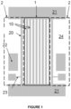
- FIG. 1 illustrates an embodiment of the thermal flux sensor, comprising two NEMS resonators arranged on either side of the network of heating nanofilaments.
- the network 1 comprises nanofilaments 10 and two beams 20 which are two nanofilaments forming the two sides of the network. Each nanofilament is embedded at each of its two ends in a support 21.
- each resonator 2 comprises an actuation device, represented in the form of an electrode 22 in the illustrated embodiment, as well as a detection device comprising a piezoresistive gauge 23.
- the two resonators are symmetrical by relative to a longitudinal axis of the network 1.
- the network of nanofilaments is configured to exhibit high sensitivity.
- the number and size of the nanofilaments are chosen so that the network has a large heat exchange surface with the surrounding fluid.
- the number of heating nanofilaments is typically between 10 and 1000.
- each heating nanofilament is arranged at a distance from an adjacent heating nanofilament.
- the distance between two adjacent nanofilaments is between 0.5 and 1.5 ⁇ m, for example of the order of 1 ⁇ m.
- the junction between the heating nanofilaments and their support is sized to minimize heat losses at this junction.
- the typical dimensions of the nanofilaments are as follows: a section whose width and height are from a few tens to hundreds of nm per side, and a length from a few ⁇ m to a few tens of ⁇ m.
- the heating nanofilaments can consist of a semiconductor material, such as silicon (monocrystalline or polycrystalline, doped or not), germanium, silicon-germanium (SiGe).
- the silicon may be porous, the porosity making it possible to increase the heat exchanges with the surrounding environment.
- the beams are made of the same material as the heating nanofilaments, possibly with different doping levels chosen so that the electrical resistance of the heating nanofilaments is greater than that of the beam.
- the beam of each NEMS resonator is constituted by a heating nanofilament does not imply that said beam necessarily has the same dimensions as the other heating nanofilaments.
- the section of the beams is of the same order of magnitude as that of the nanofilaments because the beams and the nanofilaments are preferably made with the same technology.
- the length of the beams it can be the same as that of the nanofilaments or different.
- the choice of the resonant frequency of the resonator may require the choice of a length of the beam different from the length of the other heating nanofilaments.
- the resonant frequency of each resonator is a few MHz to a few hundred MHz.
- the heating nanofilaments are shown rectilinear and parallel to each other in the appended figures, other embodiments are possible.
- the nanofilaments may not be parallel to each other; moreover, the nanofilaments can have a non-rectilinear shape, for example a serpentine shape, which makes it possible to increase the length of the heating nanofilaments while releasing any compressive stresses.
- FIG. 1 is an electrical diagram of the heat flux sensor.
- each heating nanofilament is represented in the form of an electrical resistance denoted R TCD i for the i th nanofilament, i being an integer varying between 1 and n (n being the total number of heating nanofilaments excluding the nanofilaments constituting the beams of the resonators). All the electrical resistors have substantially the same value since the nanofilaments have identical dimensions and are made of the same material.
- each beam is represented in the form of an electrical resistor denoted R NEMS 1 or R NEMS 2 .
- All of the heating beams and nanofilaments are arranged in parallel and connected by one end to a first potential (for example to ground) and by the opposite end to a second potential, denoted V TCD bias .
- Each beam is actuated in vibration at its resonant frequency by an electrode brought to an actuation potential V NEMS .
- Each piezoresistive gauge is represented in the form of an electrical resistance denoted R J1 or R J2 .
- Each gauge is current-biased, the intensity of which is denoted I bias1 or I bias2 respectively.
- I bias1 (or I bias2 ) is very small compared to the product of R NEMS 1 (or R NEMS 2 ) and V TCD bias , which is equal to the product of R TCD i and V TCD bias , then we consider that R NEMS 1 (or R NEMS 2 ) is equal to R TCD i .
- This variation in the intensity of the electric current generates a variation in the resonance frequency which is measured by the piezoresistive gauges.
- a preferred manufacturing method is based on a semiconductor on insulator (SOI, acronym for the English term “Semiconductor on insulator”) substrate.
- SOI semiconductor on insulator
- Such an SOI substrate successively comprises, from its surface, a thin layer of monocrystalline silicon (a few hundred nanometers thick), a buried dielectric layer (for example a layer of silicon oxide (SiO 2 ) and a base substrate, for example made of silicon, which serves as a mechanical support for the sensor.
- This method uses conventional microelectronics techniques, in particular photolithography, implantation, deposition and etching techniques.
- Species chosen to obtain the desired electrical resistivity are implanted in the thin layer of silicon in the zones intended to respectively form the heating nanofilaments and the resonator(s) (beam, strain gauges, actuating electrodes). These electrical resistivities may possibly be different between these two zones.
- the mechanical structures (heating nanofilaments, resonator(s) (beam, strain gauges, actuation electrodes), embeddings, etc.) are then etched anisotropically in the thin superficial silicon layer.
- the heating nanofilaments and the resonator are therefore formed in one piece with the support in said thin layer, and thus have the same thickness.
- the recesses are advantageously made large enough to ensure good mechanical strength with respect to the support after the release of the mechanical structures.
- the embedments thus typically have sides of several ⁇ m to tens of ⁇ m.
- the metallic interconnections are produced between the mechanical structures in doped silicon.
- an isotropic etching of the buried silicon oxide layer of the SOI substrate is carried out to release the mechanical silicon structures intended to be suspended (heating nanofilaments, resonator(s)) relative to the base substrate.
- the oxide layer is not etched - or is only partially etched - at the recesses.
- Said channel can be fluidically connected to the outlet of a gas chromatography column if such a column is implemented upstream of the sensor to separate and identify the compounds of the gas mixture.
- the senor can be used in a flow meter to measure gas flow.
- FIG. 3 is a block diagram of a heat flux sensor according to a variant of the sensor of the figure 1 .
- the beams 20 have a different length (lower in the figure) than that of the nanofilaments 10.
- one of the supports 21 in which the nanofilaments are embedded has an extension 210.
- One end of the beams is embedded in said extension 210 while the other end is embedded in the support 21 opposite.
- FIG 4 is a block diagram of a heat flux sensor according to a variant of the sensor of the picture 3 .
- the nanofilaments 10 are mechanically connected by bridges 11 which increase the mechanical rigidity of the network 1.
- Said bridges are advantageously made in one piece with the nanofilaments during manufacture of the network.
- the bridges extend advantageously perpendicular to the nanofilaments, although other arrangements of the bridges are possible.
- the bridges can extend parallel to each other with a distance of the order of 10 ⁇ m between two adjacent bridges.
- the beams are not connected to the other nanofilaments by such bridges, so as not to stiffen the beams and thus modify their resonance frequency and reduce the sensitivity of the resonators.
- FIG. 5 is a block diagram of a heat flux sensor according to a variant of the sensor of the picture 3 .
- the semiconductor material of the support 21, that of the resonators 2 (beams 20 and nanogauges 23) and that of the network of nanofilaments are implanted in a differentiated manner in order to adjust the electrical resistances in a differentiated manner.
- the implantation zones are schematized by the rectangles l1, l2.
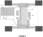
- FIG. 6 is a block diagram of a particular embodiment of the heat flux sensor.
- the structure consisting of the network of nanofilaments 10, of the resonator 2 and of the support 21 is suspended with respect to a substrate 24, which makes it possible to limit the thermal losses at the level of the recesses.
- the support 21 has a plurality of through holes 211 extending transversely to a main surface of the substrate 24. These holes 211 are distributed over at least part of the surface of the support 21. These holes can be used during process for manufacturing the sensor, to facilitate the etching of a sacrificial layer arranged under the support and the heating nanofilaments with a view to releasing the network of nanofilaments and the support and suspending them with respect to the substrate.
- each hole 211 has a diameter d 1 of the order of 0.5 ⁇ m and is separated from an adjacent hole by a distance d 2 of the order of 2 ⁇ m.
- d 1 of the order of 0.5 ⁇ m
- d 2 of the order of 2 ⁇ m.
Landscapes
- Physics & Mathematics (AREA)
- General Physics & Mathematics (AREA)
- Chemical & Material Sciences (AREA)
- Engineering & Computer Science (AREA)
- Analytical Chemistry (AREA)
- Acoustics & Sound (AREA)
- Biochemistry (AREA)
- General Health & Medical Sciences (AREA)
- Immunology (AREA)
- Life Sciences & Earth Sciences (AREA)
- Health & Medical Sciences (AREA)
- Pathology (AREA)
- Computer Hardware Design (AREA)
- Microelectronics & Electronic Packaging (AREA)
- Combustion & Propulsion (AREA)
- Micromachines (AREA)
- Investigating Or Analyzing Materials Using Thermal Means (AREA)
- Measuring Temperature Or Quantity Of Heat (AREA)
Description
La présente invention concerne un capteur de flux thermique à nanofilaments chauffants. Un tel capteur de flux thermique peut trouver une application notamment dans un capteur de gaz, un système d'analyse de gaz ou un débitmètre.The present invention relates to a thermal flux sensor with heating nanofilaments. Such a heat flux sensor can find an application in particular in a gas sensor, a gas analysis system or a flowmeter.
Un capteur de flux thermique permet de mesurer un échange de chaleur entre le corps du capteur et son milieu environnant. Le milieu environnant peut être un milieu gazeux ou liquide. Cette approche peut être utilisée pour réaliser par exemple un capteur de gaz ou un capteur de pression.A heat flux sensor makes it possible to measure a heat exchange between the body of the sensor and its surrounding environment. The surrounding medium can be a gaseous or liquid medium. This approach can be used to produce, for example, a gas sensor or a pressure sensor.
Un capteur de gaz de type TCD (acronyme du terme anglo-saxon « Thermal Conductivity Detector » ou « détecteur à conductivité thermique ») fonctionne sur le principe de la mesure de la résistance électrique d'un fil dont la température varie en fonction des échanges de chaleur avec un gaz environnant au travers de la conductivité thermique dudit gaz. Un tel capteur est décrit notamment dans le document
Un tel capteur peut être agencé à la sortie d'une colonne de chromatographie gazeuse au travers de laquelle les différentes espèces constituant un mélange de gaz à analyser sont séparées.Such a sensor can be arranged at the outlet of a gas chromatography column through which the different species constituting a mixture of gases to be analyzed are separated.
Le capteur comprend un fil chauffant couplé à une source électrique permettant de le chauffer par effet Joule, suspendu dans un volume dans lequel se trouvent une ou plusieurs espèces à détecter.The sensor comprises a heating wire coupled to an electric source making it possible to heat it by Joule effect, suspended in a volume in which there are one or more species to be detected.
Selon la nature de l'espèce en contact avec le fil chauffant, et plus précisément sa conductivité thermique, les échanges thermiques entre le fil chauffant et l'espèce sont susceptibles d'engendrer une variation de température du fil chauffant et par conséquent une variation de la résistance électrique du fil.Depending on the nature of the species in contact with the heating wire, and more precisely its thermal conductivity, the heat exchanges between the heating wire and the species are likely to cause a variation in temperature of the heating wire and consequently a variation in the electrical resistance of the wire.
Ce changement de résistance électrique, ainsi que la résistance électrique d'un fil identique en contact avec un gaz de référence, sont mesurés à l'aide d'un pont de Wheatstone, en vue de déterminer la concentration de l'espèce considérée.This change in electrical resistance, as well as the electrical resistance of an identical wire in contact with a reference gas, are measured using a Wheatstone bridge, in order to determine the concentration of the species in question.
Cependant, cette technologie présente des limites en ce qu'elle nécessite un contraste important en termes de conductivité thermique entre le gaz de référence et la ou les espèce(s) à détecter.However, this technology has limits in that it requires a large contrast in terms of thermal conductivity between the reference gas and the species or species to be detected.
Par ailleurs, le fil est généralement réalisé en platine enrobé par du nitrure, qui sont des matériaux présentant des niveaux de contraintes importants, induisant des difficultés de mise en oeuvre et des limites en termes de conception du capteur. Cette technologie est donc difficile à maîtriser en pratique.Furthermore, the wire is generally made of platinum coated with nitride, which are materials with high levels of stress, causing difficulties implementation and limitations in terms of sensor design. This technology is therefore difficult to master in practice.
Un autre type de capteur reposant sur le même principe de mesure a été réalisé sur substrat de silicium grâce à des techniques de microfabrication, permettant de graver le fil chauffant directement dans une couche de silicium. Ce type de capteur a été décrit dans les documents
En revanche, pour avoir une résistance électrique appropriée du fil de silicium, un tel capteur doit être réalisé à l'échelle nanométrique. Il en résulte que la surface d'échange thermique entre le fil chauffant et le gaz à détecter est très faible, ce qui limite lesdits échanges et la capacité du capteur à détecter de faibles concentrations de gaz.On the other hand, to have an appropriate electrical resistance of the silicon wire, such a sensor must be made at the nanometric scale. As a result, the heat exchange surface between the heating wire and the gas to be detected is very low, which limits said exchanges and the ability of the sensor to detect low concentrations of gas.
D'autres capteurs reposent sur des technologies différentes.Other sensors are based on different technologies.
Par exemple, le document
Quelle que soit la technologie considérée, des améliorations sont attendues en termes de sensibilité du capteur et de simplicité de fabrication.Whatever the technology considered, improvements are expected in terms of sensor sensitivity and manufacturing simplicity.
Un but de l'invention est de concevoir un capteur de flux thermique qui soit simple à fabriquer, tout en assurant une bonne sensibilité de détection.An object of the invention is to design a heat flux sensor which is simple to manufacture, while ensuring good detection sensitivity.
A cet effet, l'invention propose un capteur de flux thermique comprenant :
- un réseau de nanofilaments suspendus par rapport à un support, chaque nanofilament comprenant un matériau électriquement conducteur ou semi-conducteur, ledit réseau étant apte à être polarisé par une source électrique pour faire circuler un courant électrique dans chacun desdits nanofilaments,
- au moins un résonateur de type nanosystème électromécanique (NEMS) comprenant :
- * une poutre constituée d'un nanofilament formant un côté du réseau,
- * un dispositif d'actionnement apte à générer une vibration de ladite poutre sous l'effet d'un signal d'excitation,
- * un dispositif de détection configuré pour mesurer un déplacement de la poutre au cours de ladite vibration et émettre un signal de sortie présentant une résonance à la fréquence de résonance du résonateur, ladite fréquence de résonance dépendant de l'intensité du courant électrique traversant la poutre,
- a network of nanofilaments suspended relative to a support, each nanofilament comprising an electrically conductive or semi-conductive material, said network being capable of being biased by an electric source to cause an electric current to flow in each of said nanofilaments,
- at least one nano electromechanical system (NEMS) type resonator comprising:
- * a beam made of a nanofilament forming one side of the network,
- * an actuation device capable of generating a vibration of said beam under the effect of an excitation signal,
- * a detection device configured to measure a displacement of the beam during said vibration and to emit an output signal having a resonance at the resonant frequency of the resonator, said resonant frequency depending on the intensity of the electric current passing through the beam ,
Par « nanofilament » on entend dans le présent texte un filament de taille nanométrique, c'est-à-dire dont l'une des dimensions transversales (par exemple le diamètre s'agissant d'un filament rond, ou la largeur s'agissant d'un filament à section rectangulaire) est inférieure ou égale à quelques centaines de nm, par exemple inférieure à 500 nm.By “nanofilament” is meant in the present text a filament of nanometric size, that is to say of which one of the transverse dimensions (for example the diameter in the case of a round filament, or the width in the case of of a filament with a rectangular section) is less than or equal to a few hundred nm, for example less than 500 nm.
Un tel capteur repose sur le fait que la fréquence de résonance du résonateur dépend fortement de l'intensité du courant électrique qui le traverse.Such a sensor is based on the fact that the resonant frequency of the resonator strongly depends on the intensity of the electric current passing through it.
Ce capteur bénéficie de la précision de mesure offerte par les résonateurs NEMS, tout en assurant un échange de chaleur avec le gaz à détecter suffisamment important grâce au réseau de nanofilaments chauffants, cet échange de chaleur induisant une variation de la résistance électrique des nanofilaments et donc de l'intensité du courant électrique qui les traverse.This sensor benefits from the measurement precision offered by NEMS resonators, while ensuring a sufficiently large heat exchange with the gas to be detected thanks to the network of heating nanofilaments, this heat exchange inducing a variation in the electrical resistance of the nanofilaments and therefore the intensity of the electric current flowing through them.
Selon des caractéristiques avantageuses mais optionnelles de l'invention, éventuellement prises en combinaison :
- le capteur comprend au moins deux résonateurs dont les poutres sont agencées le long de deux côtés opposés du réseau de nanofilaments ;
- chaque nanofilament est encastré à ses deux extrémités dans le support ;
- tous les nanofilaments du réseau présentent la même section ;
- la section de chaque nanofilament présente une largeur et une épaisseur comprises chacune entre 10 et 500 nm ;
- chaque nanofilament est agencé à distance d'un nanofilament adjacent ;
- la distance entre deux nanofilaments adjacents est comprise entre 0,5 et 1,5 µm ;
- les poutres présentent une longueur différente de celle des autres nanofilaments ;
- chaque nanofilament est formé d'un matériau semi-conducteur, tel que du silicium ;
- les résonateurs présentent un niveau de dopage différent de celui des autres nanofilaments ;
- le support est formé du même matériau semi-conducteur que les nanofilaments, et le support présente un niveau de dopage différent de celui des nanofilaments autres que les poutres ;
- le support est formé d'un matériau différent de celui des nanofilaments, ledit matériau étant choisi pour isoler thermiquement le réseau de nanofilaments et chaque résonateur du reste du capteur ;
- le matériau du support est poreux ;
- le capteur comprend en outre un substrat par rapport auquel le support est suspendu ;
- le support présente une pluralité de trous traversants s'étendant transversalement à une surface principale du substrat ;
- les nanofilaments autres que les poutres sont reliés les uns aux autres par des pontets ;
- le nombre de nanofilaments est compris entre 10 et 1000 ;
- le dispositif d'actionnement est de type électrostatique ;
- le dispositif de détection comprend une jauge piézorésistive solidaire de la poutre.
- the sensor comprises at least two resonators whose beams are arranged along two opposite sides of the network of nanofilaments;
- each nanofilament is embedded at its two ends in the support;
- all the nanofilaments of the network have the same section;
- the section of each nanofilament has a width and a thickness each comprised between 10 and 500 nm;
- each nanofilament is arranged at a distance from an adjacent nanofilament;
- the distance between two adjacent nanofilaments is between 0.5 and 1.5 μm;
- the beams have a different length from that of the other nanofilaments;
- each nanofilament is formed from a semiconductor material, such as silicon;
- the resonators have a different level of doping from that of the other nanofilaments;
- the support is formed from the same semiconductor material as the nanofilaments, and the support has a level of doping different from that of the nanofilaments other than the beams;
- the support is formed from a material different from that of the nanofilaments, said material being chosen to thermally insulate the array of nanofilaments and each resonator from the rest of the sensor;
- the support material is porous;
- the sensor further comprises a substrate relative to which the support is suspended;
- the support has a plurality of through holes extending transversely to a main surface of the substrate;
- the nanofilaments other than the beams are connected to each other by bridges;
- the number of nanofilaments is between 10 and 1000;
- the actuation device is of the electrostatic type;
- the detection device comprises a piezoresistive gauge secured to the beam.
L'invention concerne également un capteur de gaz comprenant un capteur de flux thermique tel que décrit plus haut.The invention also relates to a gas sensor comprising a heat flux sensor as described above.
L'invention concerne également un système d'analyse de gaz comprenant une colonne de chromatographie et au moins un capteur tel que décrit ci-dessus agencé en sortie de ladite colonne de chromatographie.The invention also relates to a gas analysis system comprising a chromatography column and at least one sensor as described above arranged at the outlet of said chromatography column.
L'invention concerne également un débitmètre comprenant un capteur de flux thermique tel que décrit ci-dessus.The invention also relates to a flow meter comprising a heat flux sensor as described above.
D'autres caractéristiques et avantages de l'invention ressortiront de la description détaillée qui va suivre, en référence aux dessins annexés sur lesquels :
- la
figure 1 est un schéma d'un capteur de flux thermique selon un premier mode de réalisation de l'invention ; - la
figure 2 illustre le schéma électrique de la mesure d'un capteur selon l'invention ; - la
figure 3 est un schéma d'un capteur selon un deuxième mode de réalisation de l'invention ; - la
figure 4 est un schéma d'un capteur selon un troisième mode de réalisation de l'invention ; - la
figure 5 est un schéma d'un capteur selon un quatrième mode de réalisation de l'invention ; - la
figure 6 est un schéma d'un capteur selon un cinquième mode de réalisation de l'invention.
- there
figure 1 is a diagram of a heat flux sensor according to a first embodiment of the invention; - there
picture 2 - there
picture 3 is a diagram of a sensor according to a second embodiment of the invention; - there
figure 4 is a diagram of a sensor according to a third embodiment of the invention; - there
figure 5 is a diagram of a sensor according to a fourth embodiment of the invention; - there
figure 6 is a diagram of a sensor according to a fifth embodiment of the invention.
Les signes de référence identiques d'une figure à l'autre identifient des éléments identiques ou remplissant la même fonction. Ces éléments ne sont donc pas décrits en détail à nouveau.Identical reference signs from one figure to another identify identical elements or fulfilling the same function. These elements are therefore not described in detail again.
Pour des raisons de lisibilité des figures, les différents éléments du capteur ne sont pas nécessairement représentés à l'échelle.For reasons of readability of the figures, the various elements of the sensor are not necessarily shown to scale.
Le capteur de flux thermique comprend un réseau de nanofilaments chauffants qui sont destinés à être mis en contact avec un fluide et à échanger de la chaleur avec ledit fluide pour permettre d'en mesurer une caractéristique.The heat flux sensor comprises a network of heating nanofilaments which are intended to be brought into contact with a fluid and to exchange heat with said fluid to enable a characteristic thereof to be measured.
Les nanofilaments chauffants comprennent un matériau électriquement conducteur présentant une résistivité électrique déterminée ou un matériau semiconducteur ; ils sont connectés, par l'intermédiaire d'un support, à une source électrique adaptée pour porter lesdits nanofilaments à une température déterminée par effet Joule.The heating nanofilaments comprise an electrically conductive material having a determined electrical resistivity or a semiconductor material; they are connected, via a support, to an electrical source adapted to bring said nanofilaments to a temperature determined by the Joule effect.
Pour optimiser la sensibilité du capteur, le réseau de nanofilaments chauffants est conçu pour permettre un échange maximal de chaleur avec le fluide environnant et limiter au maximum la perte de chaleur avec le support. Les nanofilaments chauffants sont donc avantageusement suspendus par rapport au support, c'est-à-dire qu'un espace libre est ménagé entre chaque nanofilament chauffant et le support pour permettre au fluide d'entourer chaque nanofilament chauffant sur toutes ses faces et de maximiser la surface de contact entre le fluide et le nanofilament chauffant.To optimize the sensitivity of the sensor, the array of heating nanofilaments is designed to allow maximum heat exchange with the surrounding fluid and minimize heat loss with the medium. The heating nanofilaments are therefore advantageously suspended relative to the support, that is to say that a free space is left between each heating nanofilament and the support to allow the fluid to surround each heating nanofilament on all its faces and to maximize the contact surface between the fluid and the heating nanofilament.
Ainsi, dans le cas de l'application à un capteur de gaz, une modification de la composition du gaz environnant le capteur modifie les échanges de chaleur entre les nanofilaments et le gaz, et fait donc varier la température des nanofilaments chauffants ; la mesure de cette température permet d'en déduire la composition du gaz. Dans le cas de l'application à un débitmètre, une variation de vitesse d'un flux de gaz environnant le capteur modifie les échanges de chaleur entre les nanofilaments et le gaz et fait donc également varier la température des nanofilaments.Thus, in the case of the application to a gas sensor, a modification of the composition of the gas surrounding the sensor modifies the heat exchanges between the nanofilaments and the gas, and therefore causes the temperature of the heating nanofilaments to vary; the measurement of this temperature makes it possible to deduce the composition of the gas. In the case of the application to a flow meter, a speed variation of a flow of gas surrounding the sensor modifies the heat exchanges between the nanofilaments and the gas and therefore also causes the temperature of the nanofilaments to vary.
Le capteur de flux thermique combine ledit réseau de nanofilaments chauffants à au moins un résonateur de type nanosystème électromécanique (NEMS) agencé sur un côté dudit réseau et solidaire du support, ledit résonateur jouant le rôle d'un capteur de température.The thermal flow sensor combines said network of heating nanofilaments with at least one resonator of the nano electromechanical system (NEMS) type arranged on one side of said network and secured to the support, said resonator playing the role of a temperature sensor.
De manière connue en elle-même, un tel résonateur NEMS comprend une poutre suspendue par rapport au support, un dispositif d'actionnement apte à générer une vibration de ladite poutre sous l'effet d'un signal d'excitation, et un dispositif de détection configuré pour mesurer un déplacement de ladite poutre au cours de ladite vibration et émettre un signal de sortie présentant une résonance à la fréquence de résonance du résonateur, ladite fréquence de résonance dépendant de la température de la poutre.In a manner known per se, such a NEMS resonator comprises a beam suspended relative to the support, an actuation device capable of generating a vibration of said beam under the effect of an excitation signal, and a detection configured to measure a displacement of said beam during said vibration and emit an output signal having a resonance at the resonant frequency of the resonator, said resonant frequency depending on the temperature of the beam.
La poutre est un des nanofilaments chauffants du réseau, plus précisément un nanofilament situé sur un côté du réseau. Eventuellement, le capteur comprend deux résonateurs NEMS, dont la poutre respective est un nanofilament agencé sur un côté du réseau. La mise en oeuvre de deux résonateurs agencés symétriquement par rapport au réseau présente l'avantage de permettre une mesure différentielle qui simplifie le traitement des signaux de détection et permet d'améliorer le rapport signal sur bruit lors de la détection.The beam is one of the heating nanofilaments of the network, more precisely a nanofilament located on one side of the network. Optionally, the sensor comprises two NEMS resonators, the respective beam of which is a nanofilament arranged on one side of the network. The implementation of two resonators arranged symmetrically with respect to the network has the advantage of allowing a differential measurement which simplifies the detection signal processing and improves the signal to noise ratio during detection.
Le matériau des nanofilaments chauffants est caractérisé par un coefficient thermique de résistance (TCR, acronyme du terme anglo-saxon « température coefficient of résistance ») qui définit la variation de sa résistivité électrique en fonction de la température. Par conséquent, une variation de la température du réseau de nanofilaments chauffants par échange thermique avec le fluide environnant provoque une variation de la résistance électrique des nanofilaments et donc la variation de l'intensité du courant électrique qui les traverse. La poutre étant polarisée au même potentiel que les autres nanofilaments, elle subit également une variation du courant électrique qui la traverse, qui affecte fortement la fréquence de résonance du résonateur.The material of the heating nanofilaments is characterized by a thermal coefficient of resistance (TCR, acronym of the Anglo-Saxon term “temperature coefficient of resistance”) which defines the variation of its electrical resistivity as a function of temperature. Consequently, a variation in the temperature of the network of heating nanofilaments by heat exchange with the surrounding fluid causes a variation in the electrical resistance of the nanofilaments and therefore the variation in the intensity of the electric current which passes through them. The beam being polarized at the same potential as the other nanofilaments, it also undergoes a variation of the electric current which crosses it, which strongly affects the resonant frequency of the resonator.
Selon un mode de réalisation préféré, le dispositif d'actionnement est de type électrostatique. Dans ce cas, le dispositif d'actionnement comprend une électrode située d'un côté de la poutre, à distance de celle-ci. Cette distance est de l'ordre de quelques centaines de nm.According to a preferred embodiment, the actuation device is of the electrostatic type. In this case, the actuation device comprises an electrode located on one side of the beam, at a distance therefrom. This distance is of the order of a few hundred nm.
Selon un mode de réalisation préféré, le dispositif de détection est de type piézorésistif, comme décrit dans le document
La
Le réseau 1 comprend des nanofilaments 10 et deux poutres 20 qui sont deux nanofilaments formant les deux côtés du réseau. Chaque nanofilament est encastré à chacune de ses deux extrémités dans un support 21.The
Outre la poutre 20, chaque résonateur 2 comprend un dispositif d'actionnement, représenté sous la forme d'une électrode 22 dans le mode de réalisation illustré, ainsi qu'un dispositif de détection comprenant une jauge piézorésistive 23. Les deux résonateurs sont symétriques par rapport à un axe longitudinal du réseau 1.In addition to the
Le réseau de nanofilaments est configuré pour présenter une sensibilité importante. A cet effet, le nombre et la dimension des nanofilaments sont choisis pour que le réseau présente une surface d'échange thermique importante avec le fluide environnant. Ainsi, le nombre de nanofilaments chauffants est typiquement compris entre 10 et 1000. Par ailleurs, chaque nanofilament chauffant est agencé à distance d'un nanofilament chauffant adjacent. Par exemple, la distance entre deux nanofilaments adjacents est comprise entre 0,5 et 1,5 µm, par exemple de l'ordre de 1 µm. Par ailleurs, la jonction entre les nanofilaments chauffants et leur support est dimensionnée pour minimiser les pertes thermiques au niveau de cette jonction.The network of nanofilaments is configured to exhibit high sensitivity. To this end, the number and size of the nanofilaments are chosen so that the network has a large heat exchange surface with the surrounding fluid. Thus, the number of heating nanofilaments is typically between 10 and 1000. Furthermore, each heating nanofilament is arranged at a distance from an adjacent heating nanofilament. For example, the distance between two adjacent nanofilaments is between 0.5 and 1.5 μm, for example of the order of 1 μm. Furthermore, the junction between the heating nanofilaments and their support is sized to minimize heat losses at this junction.
Les dimensions typiques des nanofilaments sont les suivantes : une section dont la largeur et la hauteur sont de quelques dizaines à centaines de nm de côté, et une longueur de quelques µm à quelques dizaines de µm.The typical dimensions of the nanofilaments are as follows: a section whose width and height are from a few tens to hundreds of nm per side, and a length from a few µm to a few tens of µm.
Les nanofilaments chauffants peuvent être constitués d'un matériau semiconducteur, tel que du silicium (monocristallin ou polycristallin, dopé ou non), du germanium, du silicium-germanium (SiGe). Eventuellement, le silicium peut être poreux, la porosité permettant d'augmenter les échanges thermiques avec le milieu environnant. De manière avantageuse, les poutres sont réalisées dans le même matériau que les nanofilaments chauffants, éventuellement avec des niveaux de dopage différents choisis de sorte que la résistance électrique des nanofilaments chauffants soit supérieure à celle de la poutre.The heating nanofilaments can consist of a semiconductor material, such as silicon (monocrystalline or polycrystalline, doped or not), germanium, silicon-germanium (SiGe). Optionally, the silicon may be porous, the porosity making it possible to increase the heat exchanges with the surrounding environment. Advantageously, the beams are made of the same material as the heating nanofilaments, possibly with different doping levels chosen so that the electrical resistance of the heating nanofilaments is greater than that of the beam.
Le fait que la poutre de chaque résonateur NEMS soit constituée par un nanofilament chauffant n'implique pas que ladite poutre ait nécessairement des mêmes dimensions que les autres nanofilaments chauffants. En général, la section des poutres est du même ordre que grandeur que celle des nanofilaments car les poutres et les nanofilaments sont de préférence réalisées avec la même technologie. En ce qui concerne la longueur des poutres, elle peut être identique à celle des nanofilaments ou différente. En effet, le choix de la fréquence de résonance du résonateur peut nécessiter le choix d'une longueur de la poutre différente de la longueur des autres nanofilaments chauffants. Typiquement, la fréquence de résonance de chaque résonateur est de quelques MHz à quelques centaines de MHz.The fact that the beam of each NEMS resonator is constituted by a heating nanofilament does not imply that said beam necessarily has the same dimensions as the other heating nanofilaments. In general, the section of the beams is of the same order of magnitude as that of the nanofilaments because the beams and the nanofilaments are preferably made with the same technology. Regarding the length of the beams, it can be the same as that of the nanofilaments or different. Indeed, the choice of the resonant frequency of the resonator may require the choice of a length of the beam different from the length of the other heating nanofilaments. Typically, the resonant frequency of each resonator is a few MHz to a few hundred MHz.
Bien que les nanofilaments chauffants soient représentés rectilignes et parallèles les uns aux autres sur les figures annexées, d'autres modes de réalisation sont possibles. Par exemple, les nanofilaments peuvent ne pas être parallèles les uns aux autres ; par ailleurs, les nanofilaments peuvent présenter une forme non rectiligne, par exemple une forme de serpentin, qui permet d'augmenter la longueur des nanofilaments chauffants tout en relâchant d'éventuelles contraintes de compression.Although the heating nanofilaments are shown rectilinear and parallel to each other in the appended figures, other embodiments are possible. For example, the nanofilaments may not be parallel to each other; moreover, the nanofilaments can have a non-rectilinear shape, for example a serpentine shape, which makes it possible to increase the length of the heating nanofilaments while releasing any compressive stresses.
La
Dans ce schéma électrique, chaque nanofilament chauffant est représenté sous la forme d'une résistance électrique notée RTCD i pour le ième nanofilament, i étant un entier variant entre 1 et n (n étant le nombre total de nanofilaments chauffants en excluant les nanofilaments constituant les poutres des résonateurs). Toutes les résistances électriques présentent sensiblement la même valeur puisque les nanofilaments présentent des dimensions identiques et sont réalisés dans le même matériau.In this electrical diagram, each heating nanofilament is represented in the form of an electrical resistance denoted R TCD i for the i th nanofilament, i being an integer varying between 1 and n (n being the total number of heating nanofilaments excluding the nanofilaments constituting the beams of the resonators). All the electrical resistors have substantially the same value since the nanofilaments have identical dimensions and are made of the same material.
Dans le schéma électrique, chaque poutre est représentée sous la forme d'une résistance électrique notée RNEMS 1 ou RNEMS 2. L'ensemble des poutres et nanofilaments chauffants sont agencés en parallèle et connectés par une extrémité à un premier potentiel (par exemple à la masse) et par l'extrémité opposée à un second potentiel, noté Vpolarisation TCD.In the electrical diagram, each beam is represented in the form of an electrical resistor denoted R NEMS 1 or R NEMS 2 . All of the heating beams and nanofilaments are arranged in parallel and connected by one end to a first potential (for example to ground) and by the opposite end to a second potential, denoted V TCD bias .
Chaque poutre est actionnée en vibration à sa fréquence de résonance par une électrode portée à un potentiel Vactionnement NEMS. Chaque jauge piézorésistive est représentée sous la forme d'une résistance électrique notée RJ1 ou RJ2. Chaque jauge est polarisée en courant dont l'intensité est respectivement notée Ibias1 ou Ibias2.Each beam is actuated in vibration at its resonant frequency by an electrode brought to an actuation potential V NEMS . Each piezoresistive gauge is represented in the form of an electrical resistance denoted R J1 or R J2 . Each gauge is current-biased, the intensity of which is denoted I bias1 or I bias2 respectively.
Si Ibias1 (ou Ibias2) est très petit devant le produit de RNEMS 1 (ou RNEMS 2) et de Vpolarisation TCD, qui est égal au produit de RTCD i et de Vpolarisation TCD, alors on considère que RNEMS 1 (ou RNEMS 2) est égal à RTCD i.If I bias1 (or I bias2 ) is very small compared to the product of R NEMS 1 (or R NEMS 2 ) and V TCD bias , which is equal to the product of R TCD i and V TCD bias , then we consider that R NEMS 1 (or R NEMS 2 ) is equal to R TCD i .
Lors de la détection d'un gaz, la température du réseau de nanofilaments diminue et le courant électrique traversant le réseau de nanofilaments chauffants et les poutres varie comme les résistances électriques RTCD i = RNEMS 1 = RNEMS 2. Cette variation de l'intensité du courant électrique engendre une variation de la fréquence de résonance qui est mesurée par les jauges piézorésistives.During the detection of a gas, the temperature of the network of nanofilaments decreases and the electric current passing through the network of heating nanofilaments and the beams varies like the electric resistances R TCD i =R NEMS 1 =R NEMS 2 . This variation in the intensity of the electric current generates a variation in the resonance frequency which is measured by the piezoresistive gauges.
Pour la fabrication de ce capteur, on pourra se référer aux documents
Un procédé de fabrication préféré est basé sur un substrat semiconducteur sur isolant (SOI, acronyme du terme anglo-saxon « Semiconductor on insulator »). Un tel substrat SOI comprend successivement, à partir de sa surface, une couche mince de silicium monocristallin (de quelques centaines de nanomètres d'épaisseur), une couche diélectrique enterrée (par exemple une couche d'oxyde de silicium (SiO2) et un substrat de base, par exemple en silicium, qui sert de support mécanique au capteur.A preferred manufacturing method is based on a semiconductor on insulator (SOI, acronym for the English term “Semiconductor on insulator”) substrate. Such an SOI substrate successively comprises, from its surface, a thin layer of monocrystalline silicon (a few hundred nanometers thick), a buried dielectric layer (for example a layer of silicon oxide (SiO 2 ) and a base substrate, for example made of silicon, which serves as a mechanical support for the sensor.
Ce procédé met en oeuvre des techniques classiques de la microélectronique, en particulier des techniques de photolithographie, d'implantation, de dépôt et de gravure.This method uses conventional microelectronics techniques, in particular photolithography, implantation, deposition and etching techniques.
On implante dans la couche mince de silicium des espèces choisies pour obtenir la résistivité électrique souhaitée dans les zones destinées à former respectivement les nanofilaments chauffants et le(s) résonateur(s) (poutre, jauges de contrainte, électrodes d'actionnement). Ces résistivités électriques peuvent éventuellement être différentes entre ces deux zones.Species chosen to obtain the desired electrical resistivity are implanted in the thin layer of silicon in the zones intended to respectively form the heating nanofilaments and the resonator(s) (beam, strain gauges, actuating electrodes). These electrical resistivities may possibly be different between these two zones.
On grave ensuite de manière anisotrope les structures mécaniques (nanofilaments chauffants, résonateur(s) (poutre, jauges de contrainte, électrodes d'actionnement), encastrements, etc.) dans la couche mince de silicium superficielle. Les nanofilaments chauffants et le résonateur sont donc formés d'un seul tenant avec le support dans ladite couche mince, et présentent ainsi la même épaisseur. Les encastrements sont avantageusement réalisés suffisamment grands pour assurer une bonne tenue mécanique vis-à-vis du support après la libération des structures mécaniques. Les encastrements présentent ainsi typiquement des côtés de plusieurs µm à dizaines de µm.The mechanical structures (heating nanofilaments, resonator(s) (beam, strain gauges, actuation electrodes), embeddings, etc.) are then etched anisotropically in the thin superficial silicon layer. The heating nanofilaments and the resonator are therefore formed in one piece with the support in said thin layer, and thus have the same thickness. The recesses are advantageously made large enough to ensure good mechanical strength with respect to the support after the release of the mechanical structures. The embedments thus typically have sides of several μm to tens of μm.
Puis, par des étapes de dépôts et de gravures successives de couches électriquement isolantes (SiO2) et de couches électriquement conductrices (AISi de préférence pour les interconnexions), on réalise les interconnections métalliques entre les structures mécaniques en silicium dopé.Then, by successive deposition and etching steps of electrically insulating layers (SiO 2 ) and electrically conductive layers (AISi preferably for the interconnections), the metallic interconnections are produced between the mechanical structures in doped silicon.
On peut éventuellement ensuite former une couche planarisante de façon à faciliter l'étape ultérieure de packaging des composants par report d'un capot.It is then possible to form a planarizing layer so as to facilitate the subsequent step of packaging the components by adding a cover.
Après avoir ouvert localement (par une gravure anisotrope) cette couche planarisante au-dessus des structures mécaniques destinées à être libérées, on réalise une gravure isotrope de la couche d'oxyde de silicium enterrée du substrat SOI pour libérer les structures mécaniques en silicium destinées à être suspendues (nanofilaments chauffants, résonateur(s)) par rapport au substrat de base. La couche d'oxyde n'est en revanche pas gravée - ou est seulement partiellement gravée - au niveau des encastrements.After having locally opened (by an anisotropic etching) this planarizing layer above the mechanical structures intended to be released, an isotropic etching of the buried silicon oxide layer of the SOI substrate is carried out to release the mechanical silicon structures intended to be suspended (heating nanofilaments, resonator(s)) relative to the base substrate. The oxide layer, on the other hand, is not etched - or is only partially etched - at the recesses.
On peut alors reporter au-dessus de cette structure un capot comportant un canal gravé, créant ainsi un canal fluidique dans lequel va circuler le mélange gazeux destiné à être analysé.It is then possible to transfer above this structure a cover comprising an etched channel, thus creating a fluidic channel in which the gaseous mixture intended to be analyzed will circulate.
Ledit canal peut être relié fluidiquement à la sortie d'une colonne de chromatographie gazeuse si une telle colonne est mise en oeuvre en amont du capteur pour séparer et identifier les composés du mélange gazeux.Said channel can be fluidically connected to the outlet of a gas chromatography column if such a column is implemented upstream of the sensor to separate and identify the compounds of the gas mixture.
De manière alternative, le capteur peut être utilisé dans un débitmètre pour mesurer un débit de gaz.Alternatively, the sensor can be used in a flow meter to measure gas flow.
Naturellement, l'homme du métier pourra choisir tout autre procédé de fabrication sans pour autant sortir du cadre de la présente invention.Naturally, those skilled in the art may choose any other manufacturing process without departing from the scope of the present invention.
La
On peut ainsi optimiser séparément le réseau de nanofilaments et les résonateurs.It is thus possible to optimize the network of nanofilaments and the resonators separately.
La
La
La
Les différents modes de réalisation décrits plus haut peuvent être combinés lorsque cela est techniquement possible.The different embodiments described above can be combined when technically possible.
-
US 8,313,236US 8,313,236 -
FR 2 995 691 FR 2 995 691 -
FR 2 995 690 FR 2 995 690 -
FR 2 995 692 FR 2 995 692 -
WO 2015/082956WO 2015/082956 -
FR 2 996 219 FR 2 996 219 -
FR 3 008 690FR 3 008 690
Claims (22)
- Heat flux sensor comprising:- an array (1) of nanofilaments (10, 20) suspended from a support (21), each nanofilament comprising an electrically conductive or semiconductive material, said array being capable of being biased by an electrical source to cause an electric current to flow through each of said nanofilaments,- at least one nano-electromechanical system (NEMS) resonator (2) comprising:* a beam (20) consisting of a nanofilament forming one side of the network,* an actuating device (22) adapted to generate a vibration of said beam (20) under the effect of an excitation signal,* a sensing device configured to measure a displacement of the beam (20) during said vibration and output an output signal having a resonance at the resonator resonance frequency, said resonance frequency being dependent on the magnitude of the electric current flowing through the beam (20),
a temperature variation of the heating nanofilament network induced by a variation of a characteristic of a fluid surrounding said network causing a variation of the intensity of the current flowing through the beam resulting in a variation of the resonance frequency of said resonator. - The sensor of claim 1, comprising at least two resonators (2) whose beams (20) are arranged along two opposite sides of the nanofilament array (1).
- The sensor of either claim 1 or 2, wherein each nanofilament (10, 20) is embedded at both ends in the support (21).
- A sensor according to any of claims 1 to 3, wherein all nanofilaments (10, 20) of the array have the same cross-section.
- The sensor of any of claims 1 to 4, wherein the cross-section of each nanofilament (10, 20) has a width and a thickness each comprised between 10 and 500 nm.
- The sensor of any of claims 1 to 5, wherein each nanofilament (10, 20) is arranged at a distance from an adjacent nanofilament.
- The sensor of claim 6, wherein the distance between two adjacent nanofilaments (10, 20) is between 0.5 and 1.5 µm.
- The sensor of any of claims 1 to 7, wherein the beams (20) have a different length from that of the other nanofilaments (10).
- The sensor of any of claims 1 to 8, wherein each nanofilament (10) is formed of a semiconductor material, such as silicon.
- The sensor of claim 9, wherein each resonator has a different doping level from that of the other nanofilaments (10).
- The sensor of any of claims 9 or 10, wherein the support (21) is formed of the same semiconductor material as the nanofilaments (10), and the support (21) has a different doping level from that of the nanofilaments (10) other than the beams (20).
- The sensor according to any of claims 1 to 10, wherein the support (21) is formed of a different material from that of the nanofilaments (10), said material being selected to thermally isolate the nanofilament array (10) and each resonator (2) from the rest of the sensor.
- The sensor of claim 12, wherein the support material (21) is porous.
- The sensor of any of claims 1 to 13, further comprising a substrate (24) with respect to which the support (21) is suspended.
- The sensor of claim 14, wherein the substrate (21) has a plurality of through holes (211) extending transversely to a main surface of the substrate.
- The sensor of any of claims 1 to 15, wherein the nanofilaments (10) other than the beams (20) are connected to each other by bridges (11).
- The sensor of any of claims 1 to 16, wherein the number of nanofilaments (10, 20) is between 10 and 1000.
- The sensor of any of claims 1 to 17, wherein the actuating device is of the electrostatic type.
- The sensor of any of claims 1 to 18, wherein the sensing device comprises a piezoresistive gauge (23) integral with the beam (20).
- A gas sensor comprising a heat flux sensor according to any of claims 1 to 19.
- A gas analysis system comprising a chromatography column and at least one sensor according to any of claims 1 to 19 arranged at the outlet of said chromatography column.
- A flow meter comprising a heat flux sensor according to any of claims 1 to 19.
Applications Claiming Priority (1)
| Application Number | Priority Date | Filing Date | Title |
|---|---|---|---|
| FR1872516A FR3089630B1 (en) | 2018-12-07 | 2018-12-07 | HEATED NANOFILAMENT HEAT FLOW SENSOR |
Publications (2)
| Publication Number | Publication Date |
|---|---|
| EP3663752A1 EP3663752A1 (en) | 2020-06-10 |
| EP3663752B1 true EP3663752B1 (en) | 2023-04-05 |
Family
ID=67383804
Family Applications (1)
| Application Number | Title | Priority Date | Filing Date |
|---|---|---|---|
| EP19213402.1A Active EP3663752B1 (en) | 2018-12-07 | 2019-12-04 | Thermal flux sensor with heating filaments |
Country Status (3)
| Country | Link |
|---|---|
| US (1) | US11480480B2 (en) |
| EP (1) | EP3663752B1 (en) |
| FR (1) | FR3089630B1 (en) |
Family Cites Families (7)
| Publication number | Priority date | Publication date | Assignee | Title |
|---|---|---|---|---|
| US8313236B2 (en) | 2009-11-06 | 2012-11-20 | Agilent Technologies, Inc. | Thermal conductivity detector |
| FR2995691B1 (en) | 2012-09-19 | 2014-10-10 | Commissariat Energie Atomique | THERMAL FLOW SENSOR, GAS SENSOR COMPRISING AT LEAST ONE SUCH SENSOR AND PIRANI GAUGE COMPRISING AT LEAST ONE SUCH SENSOR |
| FR2995690B1 (en) | 2012-09-19 | 2015-04-10 | Commissariat Energie Atomique | THERMAL FLOW SENSOR WITH VIBRATION ELEMENT AND GAS SENSOR COMPRISING AT LEAST ONE SUCH SENSOR |
| FR2995692B1 (en) | 2012-09-19 | 2014-10-10 | Commissariat Energie Atomique | THERMAL FLOW SENSOR WITH INCREASED RESOLUTION |
| FR2996219B1 (en) | 2012-10-02 | 2014-10-03 | Commissariat Energie Atomique | MEASUREMENT SYSTEM COMPRISING A NETWORK OF ELECTROMECHANICAL NANO-SYSTEM TYPE RESONATORS |
| FR3008690B1 (en) | 2013-07-22 | 2016-12-23 | Commissariat Energie Atomique | DEVICE COMPRISING A FLUID CHANNEL PROVIDED WITH AT LEAST ONE MICRO OR NANOELECTRONIC SYSTEM AND METHOD OF MAKING SUCH A DEVICE |
| WO2015082956A1 (en) | 2013-12-02 | 2015-06-11 | Commissariat A L'energie Atomique Et Aux Energies Alternatives | System and method for analyzing a gas |
-
2018
- 2018-12-07 FR FR1872516A patent/FR3089630B1/en active Active
-
2019
- 2019-12-04 EP EP19213402.1A patent/EP3663752B1/en active Active
- 2019-12-06 US US16/705,405 patent/US11480480B2/en active Active
Also Published As
| Publication number | Publication date |
|---|---|
| EP3663752A1 (en) | 2020-06-10 |
| FR3089630B1 (en) | 2024-02-02 |
| US11480480B2 (en) | 2022-10-25 |
| US20200182711A1 (en) | 2020-06-11 |
| FR3089630A1 (en) | 2020-06-12 |
Similar Documents
| Publication | Publication Date | Title |
|---|---|---|
| EP2711696B1 (en) | Thermal flow sensor with vibrating element and gas sensor with at least one such thermal flow sensor | |
| EP2211185B1 (en) | Inertial sensor unit or resonant sensor with surface technology, with out-of-plane detection by strain gauge | |
| EP2309559B1 (en) | Piezoelectric actuating structure comprising an integrated piezoresistive strain gauge and manufacturing method thereof | |
| EP2711698B1 (en) | Thermal flow sensor with a membrane supported by nanowires | |
| EP2898318B1 (en) | Thermal flow sensor and gas sensor comprising at least one such sensor | |
| EP2731908B1 (en) | Miniaturised sensor comprising a heating element, and associated production method | |
| FR2977319A1 (en) | OPTIMIZED SENSIBLITY PRESSURE MEASURING DEVICE | |
| EP0194953A1 (en) | Integrated capacitive sensor for mechanical quantities, and manufacturing method | |
| FR2941525A1 (en) | GYROMETER IN SURFACE TECHNOLOGY, DETECTION OFFLINE BY MEASURING GAUGE. | |
| WO2012034951A1 (en) | Suspended-beam device and piezoresistive means for detecting the displacement thereof, and process for manufacturing the device | |
| FR2924422A1 (en) | SUSPENDED PIEZORESISTIVE STRAIN GAUGE DETECTION DEVICE COMPRISING A STRAIN AMPLIFICATION CELL. | |
| EP3424874B1 (en) | Sensor device based on nanowires with mobile mass | |
| EP2908122A1 (en) | Gas concentration sensor with suspended structure | |
| EP3663752B1 (en) | Thermal flux sensor with heating filaments | |
| EP3667309B1 (en) | Thermal flow sensor with heating wire | |
| EP4278193A1 (en) | Detection device using piezoresistive transduction | |
| EP3502676B1 (en) | Method for determining the thermal expansion coefficient of a thin crystalline film by diffraction | |
| EP3159703A1 (en) | Microelectromechanical device and system with low-impedance resistive transducer | |
| EP3910344B1 (en) | Detection device using piezoresistive transducer | |
| WO2017194509A1 (en) | Prestrained vibrating accelerometer | |
| EP4016549A1 (en) | Measurement core for measuring nuclear heating in a nuclear reactor and calorimetric sensor including such a measurement core | |
| FR3053793A1 (en) | GAS ANALYSIS DEVICE BY CATHAROMETRIC DETECTION |
Legal Events
| Date | Code | Title | Description |
|---|---|---|---|
| PUAI | Public reference made under article 153(3) epc to a published international application that has entered the european phase |
Free format text: ORIGINAL CODE: 0009012 |
|
| STAA | Information on the status of an ep patent application or granted ep patent |
Free format text: STATUS: REQUEST FOR EXAMINATION WAS MADE |
|
| 17P | Request for examination filed |
Effective date: 20191204 |
|
| AK | Designated contracting states |
Kind code of ref document: A1 Designated state(s): AL AT BE BG CH CY CZ DE DK EE ES FI FR GB GR HR HU IE IS IT LI LT LU LV MC MK MT NL NO PL PT RO RS SE SI SK SM TR |
|
| AX | Request for extension of the european patent |
Extension state: BA ME |
|
| RIN1 | Information on inventor provided before grant (corrected) |
Inventor name: LADNER, CARINE Inventor name: COLINET, ERIC Inventor name: OLLIER, ERIC Inventor name: ALAVA, THOMAS Inventor name: BENEDETTO, KEVIN |
|
| GRAP | Despatch of communication of intention to grant a patent |
Free format text: ORIGINAL CODE: EPIDOSNIGR1 |
|
| STAA | Information on the status of an ep patent application or granted ep patent |
Free format text: STATUS: GRANT OF PATENT IS INTENDED |
|
| INTG | Intention to grant announced |
Effective date: 20221103 |
|
| GRAS | Grant fee paid |
Free format text: ORIGINAL CODE: EPIDOSNIGR3 |
|
| GRAA | (expected) grant |
Free format text: ORIGINAL CODE: 0009210 |
|
| STAA | Information on the status of an ep patent application or granted ep patent |
Free format text: STATUS: THE PATENT HAS BEEN GRANTED |
|
| AK | Designated contracting states |
Kind code of ref document: B1 Designated state(s): AL AT BE BG CH CY CZ DE DK EE ES FI FR GB GR HR HU IE IS IT LI LT LU LV MC MK MT NL NO PL PT RO RS SE SI SK SM TR |
|
| REG | Reference to a national code |
Ref country code: GB Ref legal event code: FG4D Free format text: NOT ENGLISH |
|
| REG | Reference to a national code |
Ref country code: DE Ref legal event code: R096 Ref document number: 602019027141 Country of ref document: DE |
|
| REG | Reference to a national code |
Ref country code: CH Ref legal event code: EP |
|
| REG | Reference to a national code |
Ref country code: AT Ref legal event code: REF Ref document number: 1558585 Country of ref document: AT Kind code of ref document: T Effective date: 20230415 |
|
| REG | Reference to a national code |
Ref country code: IE Ref legal event code: FG4D Free format text: LANGUAGE OF EP DOCUMENT: FRENCH |
|
| REG | Reference to a national code |
Ref country code: LT Ref legal event code: MG9D |
|
| REG | Reference to a national code |
Ref country code: NL Ref legal event code: MP Effective date: 20230405 |
|
| REG | Reference to a national code |
Ref country code: AT Ref legal event code: MK05 Ref document number: 1558585 Country of ref document: AT Kind code of ref document: T Effective date: 20230405 |
|
| PG25 | Lapsed in a contracting state [announced via postgrant information from national office to epo] |
Ref country code: NL Free format text: LAPSE BECAUSE OF FAILURE TO SUBMIT A TRANSLATION OF THE DESCRIPTION OR TO PAY THE FEE WITHIN THE PRESCRIBED TIME-LIMIT Effective date: 20230405 |
|
| PG25 | Lapsed in a contracting state [announced via postgrant information from national office to epo] |
Ref country code: SE Free format text: LAPSE BECAUSE OF FAILURE TO SUBMIT A TRANSLATION OF THE DESCRIPTION OR TO PAY THE FEE WITHIN THE PRESCRIBED TIME-LIMIT Effective date: 20230405 Ref country code: PT Free format text: LAPSE BECAUSE OF FAILURE TO SUBMIT A TRANSLATION OF THE DESCRIPTION OR TO PAY THE FEE WITHIN THE PRESCRIBED TIME-LIMIT Effective date: 20230807 Ref country code: NO Free format text: LAPSE BECAUSE OF FAILURE TO SUBMIT A TRANSLATION OF THE DESCRIPTION OR TO PAY THE FEE WITHIN THE PRESCRIBED TIME-LIMIT Effective date: 20230705 Ref country code: ES Free format text: LAPSE BECAUSE OF FAILURE TO SUBMIT A TRANSLATION OF THE DESCRIPTION OR TO PAY THE FEE WITHIN THE PRESCRIBED TIME-LIMIT Effective date: 20230405 Ref country code: AT Free format text: LAPSE BECAUSE OF FAILURE TO SUBMIT A TRANSLATION OF THE DESCRIPTION OR TO PAY THE FEE WITHIN THE PRESCRIBED TIME-LIMIT Effective date: 20230405 |
|
| PG25 | Lapsed in a contracting state [announced via postgrant information from national office to epo] |
Ref country code: RS Free format text: LAPSE BECAUSE OF FAILURE TO SUBMIT A TRANSLATION OF THE DESCRIPTION OR TO PAY THE FEE WITHIN THE PRESCRIBED TIME-LIMIT Effective date: 20230405 Ref country code: PL Free format text: LAPSE BECAUSE OF FAILURE TO SUBMIT A TRANSLATION OF THE DESCRIPTION OR TO PAY THE FEE WITHIN THE PRESCRIBED TIME-LIMIT Effective date: 20230405 Ref country code: LV Free format text: LAPSE BECAUSE OF FAILURE TO SUBMIT A TRANSLATION OF THE DESCRIPTION OR TO PAY THE FEE WITHIN THE PRESCRIBED TIME-LIMIT Effective date: 20230405 Ref country code: LT Free format text: LAPSE BECAUSE OF FAILURE TO SUBMIT A TRANSLATION OF THE DESCRIPTION OR TO PAY THE FEE WITHIN THE PRESCRIBED TIME-LIMIT Effective date: 20230405 Ref country code: IS Free format text: LAPSE BECAUSE OF FAILURE TO SUBMIT A TRANSLATION OF THE DESCRIPTION OR TO PAY THE FEE WITHIN THE PRESCRIBED TIME-LIMIT Effective date: 20230805 Ref country code: HR Free format text: LAPSE BECAUSE OF FAILURE TO SUBMIT A TRANSLATION OF THE DESCRIPTION OR TO PAY THE FEE WITHIN THE PRESCRIBED TIME-LIMIT Effective date: 20230405 Ref country code: GR Free format text: LAPSE BECAUSE OF FAILURE TO SUBMIT A TRANSLATION OF THE DESCRIPTION OR TO PAY THE FEE WITHIN THE PRESCRIBED TIME-LIMIT Effective date: 20230706 Ref country code: AL Free format text: LAPSE BECAUSE OF FAILURE TO SUBMIT A TRANSLATION OF THE DESCRIPTION OR TO PAY THE FEE WITHIN THE PRESCRIBED TIME-LIMIT Effective date: 20230405 |
|
| PG25 | Lapsed in a contracting state [announced via postgrant information from national office to epo] |
Ref country code: FI Free format text: LAPSE BECAUSE OF FAILURE TO SUBMIT A TRANSLATION OF THE DESCRIPTION OR TO PAY THE FEE WITHIN THE PRESCRIBED TIME-LIMIT Effective date: 20230405 |
|
| REG | Reference to a national code |
Ref country code: DE Ref legal event code: R097 Ref document number: 602019027141 Country of ref document: DE |
|
| PG25 | Lapsed in a contracting state [announced via postgrant information from national office to epo] |
Ref country code: SK Free format text: LAPSE BECAUSE OF FAILURE TO SUBMIT A TRANSLATION OF THE DESCRIPTION OR TO PAY THE FEE WITHIN THE PRESCRIBED TIME-LIMIT Effective date: 20230405 |
|
| PGFP | Annual fee paid to national office [announced via postgrant information from national office to epo] |
Ref country code: GB Payment date: 20231221 Year of fee payment: 5 |
|
| PG25 | Lapsed in a contracting state [announced via postgrant information from national office to epo] |
Ref country code: SM Free format text: LAPSE BECAUSE OF FAILURE TO SUBMIT A TRANSLATION OF THE DESCRIPTION OR TO PAY THE FEE WITHIN THE PRESCRIBED TIME-LIMIT Effective date: 20230405 Ref country code: SK Free format text: LAPSE BECAUSE OF FAILURE TO SUBMIT A TRANSLATION OF THE DESCRIPTION OR TO PAY THE FEE WITHIN THE PRESCRIBED TIME-LIMIT Effective date: 20230405 Ref country code: RO Free format text: LAPSE BECAUSE OF FAILURE TO SUBMIT A TRANSLATION OF THE DESCRIPTION OR TO PAY THE FEE WITHIN THE PRESCRIBED TIME-LIMIT Effective date: 20230405 Ref country code: EE Free format text: LAPSE BECAUSE OF FAILURE TO SUBMIT A TRANSLATION OF THE DESCRIPTION OR TO PAY THE FEE WITHIN THE PRESCRIBED TIME-LIMIT Effective date: 20230405 Ref country code: DK Free format text: LAPSE BECAUSE OF FAILURE TO SUBMIT A TRANSLATION OF THE DESCRIPTION OR TO PAY THE FEE WITHIN THE PRESCRIBED TIME-LIMIT Effective date: 20230405 Ref country code: CZ Free format text: LAPSE BECAUSE OF FAILURE TO SUBMIT A TRANSLATION OF THE DESCRIPTION OR TO PAY THE FEE WITHIN THE PRESCRIBED TIME-LIMIT Effective date: 20230405 |
|
| PGFP | Annual fee paid to national office [announced via postgrant information from national office to epo] |
Ref country code: FR Payment date: 20231221 Year of fee payment: 5 Ref country code: DE Payment date: 20231219 Year of fee payment: 5 |
|
| PLBE | No opposition filed within time limit |
Free format text: ORIGINAL CODE: 0009261 |
|
| STAA | Information on the status of an ep patent application or granted ep patent |
Free format text: STATUS: NO OPPOSITION FILED WITHIN TIME LIMIT |
|
| 26N | No opposition filed |
Effective date: 20240108 |
|
| PG25 | Lapsed in a contracting state [announced via postgrant information from national office to epo] |
Ref country code: SI Free format text: LAPSE BECAUSE OF FAILURE TO SUBMIT A TRANSLATION OF THE DESCRIPTION OR TO PAY THE FEE WITHIN THE PRESCRIBED TIME-LIMIT Effective date: 20230405 |
|
| PG25 | Lapsed in a contracting state [announced via postgrant information from national office to epo] |
Ref country code: SI Free format text: LAPSE BECAUSE OF FAILURE TO SUBMIT A TRANSLATION OF THE DESCRIPTION OR TO PAY THE FEE WITHIN THE PRESCRIBED TIME-LIMIT Effective date: 20230405 Ref country code: IT Free format text: LAPSE BECAUSE OF FAILURE TO SUBMIT A TRANSLATION OF THE DESCRIPTION OR TO PAY THE FEE WITHIN THE PRESCRIBED TIME-LIMIT Effective date: 20230405 |
|
| REG | Reference to a national code |
Ref country code: CH Ref legal event code: PL |
|
| PG25 | Lapsed in a contracting state [announced via postgrant information from national office to epo] |
Ref country code: LU Free format text: LAPSE BECAUSE OF NON-PAYMENT OF DUE FEES Effective date: 20231204 |
|
| PG25 | Lapsed in a contracting state [announced via postgrant information from national office to epo] |
Ref country code: MC Free format text: LAPSE BECAUSE OF FAILURE TO SUBMIT A TRANSLATION OF THE DESCRIPTION OR TO PAY THE FEE WITHIN THE PRESCRIBED TIME-LIMIT Effective date: 20230405 |
|
| REG | Reference to a national code |
Ref country code: BE Ref legal event code: MM Effective date: 20231231 |
|
| PG25 | Lapsed in a contracting state [announced via postgrant information from national office to epo] |
Ref country code: MC Free format text: LAPSE BECAUSE OF FAILURE TO SUBMIT A TRANSLATION OF THE DESCRIPTION OR TO PAY THE FEE WITHIN THE PRESCRIBED TIME-LIMIT Effective date: 20230405 Ref country code: LU Free format text: LAPSE BECAUSE OF NON-PAYMENT OF DUE FEES Effective date: 20231204 |