EP3423883B1 - Optically enhanced light converter - Google Patents
Optically enhanced light converter Download PDFInfo
- Publication number
- EP3423883B1 EP3423883B1 EP16892007.2A EP16892007A EP3423883B1 EP 3423883 B1 EP3423883 B1 EP 3423883B1 EP 16892007 A EP16892007 A EP 16892007A EP 3423883 B1 EP3423883 B1 EP 3423883B1
- Authority
- EP
- European Patent Office
- Prior art keywords
- light
- layer
- planarization layer
- light conversion
- coating
- Prior art date
- Legal status (The legal status is an assumption and is not a legal conclusion. Google has not performed a legal analysis and makes no representation as to the accuracy of the status listed.)
- Active
Links
Images



Classifications
-
- G—PHYSICS
- G02—OPTICS
- G02B—OPTICAL ELEMENTS, SYSTEMS OR APPARATUS
- G02B26/00—Optical devices or arrangements for the control of light using movable or deformable optical elements
- G02B26/007—Optical devices or arrangements for the control of light using movable or deformable optical elements the movable or deformable optical element controlling the colour, i.e. a spectral characteristic, of the light
- G02B26/008—Optical devices or arrangements for the control of light using movable or deformable optical elements the movable or deformable optical element controlling the colour, i.e. a spectral characteristic, of the light in the form of devices for effecting sequential colour changes, e.g. colour wheels
-
- B—PERFORMING OPERATIONS; TRANSPORTING
- B32—LAYERED PRODUCTS
- B32B—LAYERED PRODUCTS, i.e. PRODUCTS BUILT-UP OF STRATA OF FLAT OR NON-FLAT, e.g. CELLULAR OR HONEYCOMB, FORM
- B32B3/00—Layered products comprising a layer with external or internal discontinuities or unevennesses, or a layer of non-planar shape; Layered products comprising a layer having particular features of form
- B32B3/26—Layered products comprising a layer with external or internal discontinuities or unevennesses, or a layer of non-planar shape; Layered products comprising a layer having particular features of form characterised by a particular shape of the outline of the cross-section of a continuous layer; characterised by a layer with cavities or internal voids ; characterised by an apertured layer
- B32B3/263—Layered products comprising a layer with external or internal discontinuities or unevennesses, or a layer of non-planar shape; Layered products comprising a layer having particular features of form characterised by a particular shape of the outline of the cross-section of a continuous layer; characterised by a layer with cavities or internal voids ; characterised by an apertured layer characterised by a layer having non-uniform thickness
-
- H—ELECTRICITY
- H04—ELECTRIC COMMUNICATION TECHNIQUE
- H04N—PICTORIAL COMMUNICATION, e.g. TELEVISION
- H04N9/00—Details of colour television systems
- H04N9/12—Picture reproducers
- H04N9/31—Projection devices for colour picture display, e.g. using electronic spatial light modulators [ESLM]
- H04N9/3102—Projection devices for colour picture display, e.g. using electronic spatial light modulators [ESLM] using two-dimensional electronic spatial light modulators
- H04N9/3111—Projection devices for colour picture display, e.g. using electronic spatial light modulators [ESLM] using two-dimensional electronic spatial light modulators for displaying the colours sequentially, e.g. by using sequentially activated light sources
- H04N9/3114—Projection devices for colour picture display, e.g. using electronic spatial light modulators [ESLM] using two-dimensional electronic spatial light modulators for displaying the colours sequentially, e.g. by using sequentially activated light sources by using a sequential colour filter producing one colour at a time
-
- Y—GENERAL TAGGING OF NEW TECHNOLOGICAL DEVELOPMENTS; GENERAL TAGGING OF CROSS-SECTIONAL TECHNOLOGIES SPANNING OVER SEVERAL SECTIONS OF THE IPC; TECHNICAL SUBJECTS COVERED BY FORMER USPC CROSS-REFERENCE ART COLLECTIONS [XRACs] AND DIGESTS
- Y10—TECHNICAL SUBJECTS COVERED BY FORMER USPC
- Y10T—TECHNICAL SUBJECTS COVERED BY FORMER US CLASSIFICATION
- Y10T428/00—Stock material or miscellaneous articles
- Y10T428/24—Structurally defined web or sheet [e.g., overall dimension, etc.]
- Y10T428/24355—Continuous and nonuniform or irregular surface on layer or component [e.g., roofing, etc.]
- Y10T428/24364—Continuous and nonuniform or irregular surface on layer or component [e.g., roofing, etc.] with transparent or protective coating
-
- Y—GENERAL TAGGING OF NEW TECHNOLOGICAL DEVELOPMENTS; GENERAL TAGGING OF CROSS-SECTIONAL TECHNOLOGIES SPANNING OVER SEVERAL SECTIONS OF THE IPC; TECHNICAL SUBJECTS COVERED BY FORMER USPC CROSS-REFERENCE ART COLLECTIONS [XRACs] AND DIGESTS
- Y10—TECHNICAL SUBJECTS COVERED BY FORMER USPC
- Y10T—TECHNICAL SUBJECTS COVERED BY FORMER US CLASSIFICATION
- Y10T428/00—Stock material or miscellaneous articles
- Y10T428/24—Structurally defined web or sheet [e.g., overall dimension, etc.]
- Y10T428/24355—Continuous and nonuniform or irregular surface on layer or component [e.g., roofing, etc.]
- Y10T428/24372—Particulate matter
Definitions
- the present invention relates to a light converter comprising a solid-state light conversion material, which may form part of an optical device such as a phosphor wheel.
- a method of manufacturing a light converter is also provided.
- Light conversion (or wavelength conversion) materials such as phosphors are used in a variety of applications, especially in optical devices.
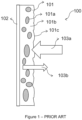
- a schematic depiction of a cross-section of an existing exemplary light converter 100 is shown in Figure 1 .
- the light conversion layer 101 conventionally comprises phosphor particles (powder) 101a in a polymer binder, such as cured silicone glue 101b. This is known as a phosphor-in-silicone (PIS) type.
- PIS phosphor-in-silicone
- the phosphor particles 101a are dispersed in liquid transparent silicone 101b by dispensing, screen printing or another coating method and then thermally cured and solidified.
- the light conversion layer 101 has a rough surface 101c on its side opposite to that on which the highly reflective coating 102 is provided.
- Excitation light 103a is incident on the light conversion layer 101 and the phosphor powder 101a converts this into emission light.
- the highly reflective coating 102 captures this emission light from all possible directions and reflects it, so that the emission light 103b all travels in the opposite direction to the excitation light 103a.
- the light converter 100 is of a reflective type. It is also known to provide a light conversion layer 101 without highly reflective coating 102 and such light converters are of a transmissive type.
- a phosphor wheel which is an optical device for generating emission light of one or typically multiple different wavelengths from excitation light of a single light source (typically of a narrow range of wavelengths).
- An example phosphor wheel is described in WO-2014/016574 , having common inventorship.
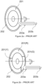
- a light converter 201 is provided on a disc substrate 202.
- the light converter 201 is of PIS type, in accordance with Figure 1 .
- the light converter 201 is formed as a single colour phosphor ring (in a concentric pattern, as shown in Figure 2a) or multiple colour segments 201(R) (red), 201(Y) (yellow) and 201(G) (green), each of which is used to generate light with a specific colour (shown in Figure 2b ).
- the light converter 201 converts the light spectrum from excitation light of a first range of spectral wavelength to emission (or re-emission) light of a second, different range of spectral wavelengths.
- Excitation light 203a source light, for example blue light
- emission light 203b for instance, yellow light, particularly in the case of 201(Y)
- the emission light 203b is reflected by the disc substrate 202 and the emission light 203b is collected by a lens system (not shown).
- the disc substrate 202 is rotated during use, although this device can be used in a static (non-rotating) configuration, in which case it may not be known as a phosphor wheel.
- EP 2 645 433 A2 discloses a wave-length conversion inorganic member with reduced limitation for the thickness, shape, and the type of the inorganic phosphor used.
- a light emitting element includes a base material having a rough surface and a phosphor layer which is directly or indirectly formed on the rough surface of the base material and includes a plurality of phosphor particles which are bonded to each other by a binder.
- WO 2015/180630 A1 discloses a wavelength conversion device, comprising a substrate, a reflecting layer, and a light-emitting layer superimposed successively.
- the light-emitting layer contains a wavelength conversion material and a second binder
- the reflecting layer contains reflecting particles, auxiliary particles, and a first binder.
- the reflecting particles are used for reflecting light
- the auxiliary particles are used for filling voids between the reflecting particles.
- the first binder is used for binding the reflecting particles and auxiliary particles into a layer.
- WO 2014/030342 A1 discloses a LED device comprising a light emitting member that emits light, a light diffusing member that diffuses light from the light emitting member, and an adhesive layer to which the light emitting member and the light diffusing member are bonded .
- the light emitting member includes a package, an LED chip mounted on the package, and a wavelength conversion layer.
- the light diffusion member includes a glass substrate and a light diffusion layer.
- the binder of the light diffusing layer is a ceramic material which is a cured product of an organosilicon compound.
- PIS-type light conversion layers with solid-state light conversion materials, such as ceramic converters or phosphor glass.
- PIS-type materials have advantages over such solid-state light conversion materials. For example, they may allow a more flexible choice of colours, a simpler structure and lower cost. It would be advantageous to provide performance improvements without changing the type of light conversion layer being used.
- light converter comprising at least one optical coating on a light conversion layer, in which the light conversion layer comprises light conversion particles (for instance, phosphor powder) in a polymer binding material (for example, a polymer such as silicone) may be advantageous.
- a planarization layer is advantageously provided on a first surface of the light conversion layer.
- the planarization layer comprises a polymer material, an organic material, or a composite material, wherein the planarization layer has a refractive index, wherein the difference between the refractive index of the planarization layer and the refractive index of the light conversion layer is no more than 10% of the refractive index of the light conversion layer.
- the light converter further comprises at least one optical coating as part of or on a surface of the planarization layer.
- the surface of the planarization layer is optically smooth and/or relatively smooth in comparison with the first surface of the light conversion layer (adjacent the planarization layer).
- a light conversion layer formed of phosphor particles in a binder may have a rough surface and it may be difficult to coat this surface with such an optical coating.
- the planarization layer has a smoother surface, for instance an optically smooth surface, on which the optical coating (or coatings) can be applied more readily. For instance, it may have a roughness average (Ra) of no greater than 0.02 ⁇ m.
- the planarization layer may comprise comprises a silicone material, an organic material or a composite material.
- the planarization layer may be deposited by dispensing, spraying, brushing, sputtering, spin coating or silk or screen printing.
- the planarization layer is cured, in particular by thermal curing.
- the thermal curing may be at a low temperature, for instance no greater than 150C and/or for a long time, for example at least 1 or 2 hours. This may allow the planarization layer to form as a smooth layer without affecting the light conversion layer beneath.
- the optical coating may be a thin film coating such an anti-reflective (AR) coating, a high-reflective (HR) coating, a dichroic filter (DF) coating and/or a metallic coating.
- An optical coating may improve the performance of the light converter (in terms of efficiency) by 5%, whilst reducing the operating temperature significantly, for instance by around 9C.
- FIG. 3 there is schematically illustrated a cross-section view of an embodiment of a light converter 300. There is shown: a light conversion layer 301; a highly reflective coating layer 302; a planarization layer 304; and an optical coating 305.
- the light conversion layer 301 is formed on the highly reflective coating layer 302.
- the light conversion layer 301 comprises phosphor particles (powder) 301a in a polymer binder, such as cured silicone glue 301b.
- this light conversion layer 301 is of phosphor-in-silicone (PIS) type.
- the light conversion layer 301 has a granular, rough surface 301c on one side opposite to that on which the highly reflective coating 302 is provided.
- excitation light 303a is incident on the light conversion layer 301, which converts this into light of a different wavelength, then reflected by the highly reflective layer 302 to provide emission light 303b.
- the planarization layer 304 is deposited on rough surface 301c of the light conversion layer 301.
- the planarization layer 304 is a silicone adhesive.
- the application and/or thickness of the planarization layer 304 is controlled so that an optical surface (optically smooth) is achieved in microscopic dimensions.
- the roughness average (Ra) of the planarization layer 304 may be less than 0.02 ⁇ m.
- the thickness of the planarization layer 304 can be made sufficient to make this layer optically smooth, for example 400 nm to 1000 nm or as thick as up to (and optionally including) 100 ⁇ m, 150 ⁇ m or 200 ⁇ m (400nm, 1 ⁇ m, 100 ⁇ m or 150 ⁇ m may optionally be minimum thicknesses).
- It is cured to provide a firm, dry surface for better handling. Thermal curing at temperature under 150C for 1 or 2 hours is used. This temperature limitation is particularly to avoid damaging the light conversion layer 301 beneath.
- the optical coating 305 is a thin film coating, such as an anti-reflective, AR, coating. This is applied after the planarization layer 304 has been cured. PVD is used to apply this coating.
- the AR coating 305 is applied on the side of the light conversion layer 301 to be exposed to the excitation light 303a. This is intended to reduce the reflection loss of excitation light 303a at the interface with the light conversion layer 301.
- the thickness of this coating is based on the design performance, the thin-film materials used and the properties of the adjacent materials, such as the planarization layer 304.
- the planarization layer 304 and optical coating 305 can provide a further, secondary benefit.
- the planarization layer 304 has a low refractive index, typically lower than that of the light conversion layer 301. This increases the angle of emission light 303b collection into and/or light emergence from the light conversion layer 301 (to at least 30 degrees relative a normal to the surface). Therefore, the total extraction of converted light is improved.
- the highly reflective coating layer 302 is optional and an embodiment without such a layer is discussed below.
- the structure of the light conversion layer 301 may be varied to any type of particle-in-binder configuration. Such structures tend to form with a rough outer surface, which may cause problems if an optical coating is applied.
- the planarization layer 304 need not be formed from silicone. Desirable properties for this layer may include one of more of: low absorption; high transmission (at least 50%, 60%, 70%, 75%, 80%, 85%, 90% or 95%) in a wide band (380nm to 800nm); capable of forming an optically smooth surface readily; low cost; easy to manufacture. Other materials, especially comprising SiO 2 and/or Al 2 O 3 may be used.
- the refractive index of the planarization layer 304 could be less than that of the light conversion layer 201 and optionally it is as low as possible (less than 1.3, 1.25, 1.2, 1.1 or 1.05), whilst still allowing a reliable optical film to be formed upon it.
- the refractive index may be set dependent on the optical coating being used and a high refractive index may be preferred when an AR coating is used.
- the refractive index of the planarization layer 304 may be set to be close to or match that of the light conversion layer 301.
- a YAG phosphor has a high refractive index of 1.7 or more.
- the phosphor distributed in a silicone resin typically has a refractive index of about 1.4 to 1.5, to form the light conversion layer 301. Due to the difference in refractive indices, a considerable proportion of light may be scattered at the interface between these layers.
- planarization layer 304 is preferred to have a specific refractive index
- an alternative approach is for an optical coating to be formed on the planarization layer 304 with the desired refractive index.
- the planarization layer 304 may be formed by any silicone adhesive process (such as spraying) but alternatives may include dispensing, brushing, sputtering, spin coating or silk or screen printing.
- Sol-gel/dip coating, CVD, magneto sputtering PVD (which may provide good film density) or other techniques may alternatively be used for depositing the planarization layer.
- RTV room temperature vulcanisation
- optical coating may be provided on the planarization layer 304, such as: a highly-reflective (HR) coating (not typically used); a dichroic filter (DF) coating (for filtering the excitation and/or emission light); and/or a metallic coating (such as, such as AIFlex (TM) or SilFlex (TM), again not typically used).
- HR highly-reflective
- DF dichroic filter
- TM SilFlex
- Dip coating may be used in addition or as an alternative to PVD to apply the optical coating.
- Other known techniques may be possible.
- a light converter comprising: a light conversion layer, comprising light conversion particles in a binding material, for generating emission light from excitation light incident on the light conversion layer; and a planarization layer on a surface of the light conversion layer.
- a surface of the planarization layer is optically smooth and/or smoother than the surface of the light conversion layer.
- At least one optical coating is beneficially part of or on the smooth surface of the planarization layer.
- the surface of the planarization layer has a roughness that is lower than a specific value and/or than a roughness of the surface of the light conversion layer (adjacent the planarization layer). The optical coating can then be applied to the planarization layer or formed together with the planarization layer.
- a method of manufacturing a light converter comprising: depositing a planarization layer described above on a first surface of a light conversion layer, the light conversion layer comprising light conversion particles in a polymer binding material and generating emission light from excitation light incident on the first surface of the light conversion layer; and applying at least one optical coating to or forming at least one optical coating in a surface of the planarization layer.
- the surface of the planarization layer is beneficially relatively smooth in comparison with the surface of a light conversion layer. This method may have steps for providing any of the features described herein with respect to the light converter.
- the surface of the light conversion layer could have a roughness as described herein with reference to the planarization layer.
- This might be achieved by smoothing the (PIS) light conversion layer surface, for example by dispensing and/or curing appropriately and moulding before final solidification of the (silicone) material.
- no planarization layer would be necessary.
- the optical coating for example a silicon dioxide coating of about 1 ⁇ m thickness, could then be deposited directly on the light conversion layer surface.
- this approach is difficult to implement in manufacturing and the performance is not as good as when an additional planarization layer is provided.
- the light conversion particles are typically phosphor particles.
- the binding material is preferably a polymer.
- it may comprise a silicone material.
- the planarization layer may comprise (or be formed from) the same material as the binding material.
- the surface of the planarization layer is typically configured to be optically smooth. This may be over a wide angle of light incidence (at least 5, 10, 15, 20, 25, 30, 35, 40 or 45 degrees from the surface) and/or a wide range of wavelengths (380nm to 800nm or at least the wavelength of excitation light and/or emission light). For example, it may have a roughness average (Ra) of no greater (or less) than 0.03 ⁇ m, 0.025 ⁇ m, 0.02 ⁇ m, 0.015 ⁇ m, 0.01 ⁇ m or 0.005 ⁇ m.
- the surface of the planarization layer may have a Ra that is no more than 0.5, 0.4, 0.3, 0.25, 0.2, 0.1 or 0.05 of a Ra of the surface of the light conversion layer. Additionally or alternatively, the surface of the planarization layer may have a Ra that is no more than 0.3, 0.25, 0.2, 0.1, 0.05 or 0.01 of a wavelength of the excitation light or emission light.
- the planarization layer can have an optical refractive index that is lower than, similar to, or greater than that of the light conversion layer. Typically, the difference between the refractive index of the planarization layer and the refractive index of the light conversion layer should be less (or no more) than 10%, preferably 5% of the refractive index of the light conversion layer. Additionally or alternatively, the optical refractive index of the planarization layer may, in some embodiments be less (or no more than) than and in other embodiments greater than (or at least) 1.7, 1.6, 1.5, 1.4, 1.3, 1.25, 1.2, 1.1 or 1.05.
- the planarization layer may comprise a silicone material, an organic material or a composite material. It may comprise SiOz and/or Al 2 O 3 .
- the planarization layer may be deposited by any one or more of: dispensing, spraying, brushing, sputtering, silk printing or screen printing.
- the planarization layer may further be cured, for instance by thermal curing or room temperature vulcanisation (RTV).
- the thermal curing may be at a temperature no greater (or less) than 150C.
- the duration of the thermal curing may be around or at least 1 or 2 hours.
- the at least one optical coating preferably comprises a thin film coating.
- the at least one optical coating may comprise one or more of: an anti-reflective (AR) coating; a high-reflective (HR) coating; a dichroic filter (DF) coating; and a metallic coating.
- AR anti-reflective
- HR high-reflective
- DF dichroic filter
- the planarization layer is on a first surface of the light conversion layer.
- the light converter may further comprise an optically functional layer on a second surface of the light conversion layer (typically opposite the first surface of the light conversion layer).
- the optically functional layer may comprise a highly reflective material or a reflective resin layer.
- the light converter is preferably implemented as part an optical device.
- the optical device may comprise a substrate. Then, the light converter may be provided on (mounted on or attached to) the substrate.
- the substrate may comprise (or be formed of) a metal material, a non-metallic material or a composite material.
- the optical device may be one of: a colour wheel; a phosphor wheel; a projection display; and an automotive headlight.
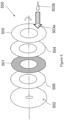
- FIG. 4 there is depicted an exploded schematic of a first phosphor wheel 400 embodiment.
- This comprises: a substrate 402; a light conversion layer 401; a planarization layer 404; and an optical coating 405.
- the substrate 402 is a metal disk, coating with a highly reflective film.
- the light conversion layer 401 is of PIS type (as discussed above) and is typically applied to the substrate 402 by dispensing, screen printing or another coating method. The layer is then thermally cured and solidified to form colour segments or a colour ring.
- the planarization layer 404 is formed of silicone to provide an optically smooth surface on which the optical coating, which is an AR and/or DF coating, is applied.
- the constructed colour/phosphor wheel module is mounted on a motor to rotate with high speed.
- the formation of the light conversion layer 401, planarization layer 404 and optical coating 405 is in accordance with that described for Figure 3 .
- the substrate 402 need not have a highly reflective film. It may be a metallic, reflective substrate. Alternatively, no reflective layer may be provided on the side of the light conversion layer 401 opposite to that of the planarization layer 404.
- the substrate may be (fully or partially) optically transparent. Then, the colour/phosphor wheel may be of a transmissive type.
- the substrate 402 need not be mounted on a motor and/or rotated. Instead, it may be used in a static (non-rotating) configuration.
- planarization layer may combine the planarization layer and optical coating as one layer. If the planarization layer is chosen to have a refractive index roughly half-way between the two surrounding media (that is the wavelength conversation layer below, typically phosphor in silicon, and air above respectively), with a judicious choice of thickness for this layer, a layer could be formed which is both smooth and a single layer AR coating. Additionally or alternatively, if the planarization layer were made thin enough, it could become part of the thin film stack, for instance making it part of the AR coating design. Its index and thickness may then be controlled as needed by the AR coating design.
- the phosphor wheel 500 comprises: a substrate 502; a light conversion layer 501; a planarization layer 504; an optical coating 505; and a highly reflective silicone layer 506.
- the highly reflective silicone layer 506 may be considered a reflective resin layer, as described in our co-pending International (PCT) patent application no. PCT/CN2015/097366 , the contents of which are incorporated herein by reference.
- the embodiment of Figure 5 may be considered an implementation of the light converter of this disclosure in combination with the reflective resin layer as described in the co-pending patent application.
- the highly reflective silicone layer 506 is a silicone material, sold under the name CI-2001 by Dow Corning Corporation. Further information about this material may be found on its Technical Data Sheet and Safety Data Sheet, the contents of which are incorporated by reference.
- the main constituent of this material is octamethyltrisiloxane (which is a reflective resin) and it also comprises: titanium dioxide (concentration around 20 to 30%, Refractive Index 2.1); silicon dioxide (around 1 to 5%, Rl 1.47); and aluminum hydroxide (around 1 to 5%, Rl 1.8). These additional constituents may be further active ingredients for light diffusive reflection.
- This material cures at room temperature to a tough, resilient and non-tacky surface and has low flammability, although a mild heat acceleration (after solvent flash-off) can speed in-line processing.
- the material also has a low viscosity that enhances flow and fills in narrow gaps and spaces.
- a suitable material should be operational over a temperature range of -45 to 200°C (-49 to 392°F) for long periods of time (at least 1500 hours).
- a suitable material should be operational over a temperature range of -45 to 200°C (-49 to 392°F) for long periods of time (at least 1500 hours).
- behaviour of the materials and performance in particular applications can become more complex and require additional considerations. Factors that may influence performance are configuration and stress sensitivity of components, cooling rates and hold times and prior temperature history.
- the durability of the cured silicone elastomer is time and temperature dependent.
- the silicone material is mixed with an organic solvent before coating, which in this case comprises methyl siloxane and is sold by Dow Corning Corporation under the name OS-20. Further information about this material may be found on its Technical Data Sheet and Safety Data Sheet, the contents of which are incorporated by reference. This is a volatile solvent and is used as dilution to adjust the solution viscosity.
- the mixed silicone material is prepared as homogeneous according to process requirements and silicon oil thinner is added to adjust the viscosity before putting this into a mixing machine to do the mix. A two-step mixing program for the mixture machine is recommended, with 600 RPM low speed for 60s then 1200 RPM high speed for 120s.
- the silicone layer is formed on the substrate 502 by dispensing, spray coating or screen printing.
- Room temperature curing or room temperature vulcanization (RTV) is normally used, but the cure rate can be accelerated (and the time required to reach a tack-free state may be reduced) by mild heat.
- Thermal curing can alternatively be used. Atmospheric moisture may assist the cure. Adequate time for the solvent to evaporate prior to exposing to elevated temperatures in an air circulating oven should be allowed.
- a typical cure schedule for 3 mil (75 micron) coatings is 10 minutes at room temperature, followed by 10 minutes at 60°C. If the coating blisters or contains bubbles, additional time at room temperature is allowed for the solvent to flash off prior to oven cure.
- the pot life of the silicone material is dependent on the application method chosen.
- the reflective resin layer may comprise a mixed inorganic-organic polymer or elastomer (and may be a layer consisting of such a polymer or elastomer).
- the reflective resin layer comprises silicone and more preferably the reflective resin layer is a silicone layer.
- the reflective resin layer may comprise a siloxane, such as octamethytrisiloxane.
- the reflective resin layer may comprise other constituent substances such as at least one further optically reflective material, but a reflective resin material should be the optically dominant and/or majority (by concentration or w/w, for instance) component of the layer.
- the reflective resin may form at least (or greater than) 50% of the reflective resin layer (by concentration or w/w).
- optically reflective materials that may be present can comprise or include one or more of: titanium dioxide; silicon dioxide; and aluminum hydroxide.
- the thickness of the reflective resin layer is generally at least (or greater than) about 0.05mm and typically no more (or less than) about 0.15mm and more preferably at least about 0.1mm and/or around 0.1mm (for example 0.08mm or 0.09mm to 0.11 mm or 0.12mm).
- the light conversion layer 501 is formed as a PIS layer in the manner described above, with reference to Figure 3 .
- this forms colour segments or a colour as the light conversion layer 501 on the silicone reflective layer 502.
- the silicone planarization layer 504 is coated and solidified on the light conversion layer 501, again as detailed with reference to Figure 3 .
- This forms the optical smooth surface, upon which the thin film optical coating 505 is applied, which typically comprises an AR and/or DF coating.
- the colour/phosphor wheel module is mounted on a motor to rotate with high speed.
- the substrate may be coated with an optically functional layer.
- the light conversion layer may be provided on the substrate by providing the light conversion layer on the optically functional layer.
- the optically functional layer may be a reflective resin layer, as discussed above.
- any of the alternatives described above with reference to the light converter of Figure 3 and/or the colour/phosphor wheel of Figure 4 may equally be applied to the embodiment of Figure 5 .
- the highly reflective silicone layer 506 may be replaced by an alternative optically functional layer. This layer may be highly reflective and/or made of a material other than silicone.
- the optically functional layer (whether a silicone layer or otherwise) may be applied to the substrate 502 by other coating methods, for instance any of those discussed above with reference to the application of light conversion and/or planarization layers.
- FIG. 6 there is illustrated a schematic of a configuration for testing the phosphor wheel embodiments of Figures 4 and 5 .
- This configuration comprises: first laser diode bank 601a; second laser diode bank 601b; filter 610; lens system 620, 621, 622, 623; dichroic mirror 630; monitor power meter 640; output power meter 650; and phosphor wheel 660.
- the first laser diode bank 601a and second laser diode bank 601b provide light with a total power of 60W.
- the light from the two laser diode banks 601a and 601b is directed, via filter 610, to provide input light 615 to a first lens system 620.
- the output light 681 from the first lens system 620 is incident on the dichroic mirror 630.
- the output light 681 is split into: measurement light 682, which is provided to the monitor power meter 640 via second lens system 621; and test light 683, which is provided as excitation light to the phosphor wheel 660 via third lens system 622.
- the emission light 684 from the phosphor wheel 660 is returned to the dichroic mirror 630, where it is reflected to provide input light 685 to the output power meter 650 via a fourth lens system 623.
- an efficiency performance for the phosphor wheel can be identified, which can be compared with other phosphor wheels for illustrative purposes. Using such a configuration, the 5% performance improvement between an implementation in accordance with Figure 2a and an implementation in accordance with Figure 4 was observed.
Landscapes
- Physics & Mathematics (AREA)
- Astronomy & Astrophysics (AREA)
- Spectroscopy & Molecular Physics (AREA)
- General Physics & Mathematics (AREA)
- Optics & Photonics (AREA)
- Engineering & Computer Science (AREA)
- Multimedia (AREA)
- Signal Processing (AREA)
- Optical Filters (AREA)
- Non-Portable Lighting Devices Or Systems Thereof (AREA)
- Projection Apparatus (AREA)
- Surface Treatment Of Optical Elements (AREA)
Description
- The present invention relates to a light converter comprising a solid-state light conversion material, which may form part of an optical device such as a phosphor wheel. A method of manufacturing a light converter is also provided.
- Light conversion (or wavelength conversion) materials such as phosphors are used in a variety of applications, especially in optical devices. A schematic depiction of a cross-section of an existing
exemplary light converter 100 is shown inFigure 1 . This comprises: alight conversion layer 101; and a highlyreflective coating 102. Thelight conversion layer 101 conventionally comprises phosphor particles (powder) 101a in a polymer binder, such as curedsilicone glue 101b. This is known as a phosphor-in-silicone (PIS) type. Thephosphor particles 101a are dispersed in liquidtransparent silicone 101b by dispensing, screen printing or another coating method and then thermally cured and solidified. Thelight conversion layer 101 has arough surface 101c on its side opposite to that on which the highlyreflective coating 102 is provided. -
Excitation light 103a is incident on thelight conversion layer 101 and thephosphor powder 101a converts this into emission light. The highlyreflective coating 102 captures this emission light from all possible directions and reflects it, so that theemission light 103b all travels in the opposite direction to theexcitation light 103a. Thus, thelight converter 100 is of a reflective type. It is also known to provide alight conversion layer 101 without highlyreflective coating 102 and such light converters are of a transmissive type. - One application of such a light converter is a phosphor wheel, which is an optical device for generating emission light of one or typically multiple different wavelengths from excitation light of a single light source (typically of a narrow range of wavelengths). An example phosphor wheel is described in
WO-2014/016574 , having common inventorship. - Referring next to Figures 2a and
2b , there is shown first and second examples respectively of known phosphor wheel structures in a schematic form. The two examples have similar features and where the same features are shown, identical reference numerals have been used. Alight converter 201 is provided on adisc substrate 202. Thelight converter 201 is of PIS type, in accordance withFigure 1 . Thelight converter 201 is formed as a single colour phosphor ring (in a concentric pattern, as shown in Figure 2a) or multiple colour segments 201(R) (red), 201(Y) (yellow) and 201(G) (green), each of which is used to generate light with a specific colour (shown inFigure 2b ). Thelight converter 201 converts the light spectrum from excitation light of a first range of spectral wavelength to emission (or re-emission) light of a second, different range of spectral wavelengths.Excitation light 203a (source light, for example blue light) causes the generation ofemission light 203b (for instance, yellow light, particularly in the case of 201(Y)), when it is incident on thelight converter 201. Theemission light 203b is reflected by thedisc substrate 202 and theemission light 203b is collected by a lens system (not shown). Typically, thedisc substrate 202 is rotated during use, although this device can be used in a static (non-rotating) configuration, in which case it may not be known as a phosphor wheel. -
EP 2 645 433 A2 discloses a wave-length conversion inorganic member with reduced limitation for the thickness, shape, and the type of the inorganic phosphor used. -
US 2015/276177 A1 a light emitting element includes a base material having a rough surface and a phosphor layer which is directly or indirectly formed on the rough surface of the base material and includes a plurality of phosphor particles which are bonded to each other by a binder. -
WO 2015/180630 A1 discloses a wavelength conversion device, comprising a substrate, a reflecting layer, and a light-emitting layer superimposed successively. The light-emitting layer contains a wavelength conversion material and a second binder, and the reflecting layer contains reflecting particles, auxiliary particles, and a first binder. The reflecting particles are used for reflecting light, and the auxiliary particles are used for filling voids between the reflecting particles. The first binder is used for binding the reflecting particles and auxiliary particles into a layer. -
WO 2014/030342 A1 discloses a LED device comprising a light emitting member that emits light, a light diffusing member that diffuses light from the light emitting member, and an adhesive layer to which the light emitting member and the light diffusing member are bonded . The light emitting member includes a package, an LED chip mounted on the package, and a wavelength conversion layer. The light diffusion member includes a glass substrate and a light diffusion layer. In the LED device, the binder of the light diffusing layer is a ceramic material which is a cured product of an organosilicon compound. - Improving the performance, especially in terms of efficiency, output power and temperature management of light converters, particularly for use in phosphor wheels, is a significant challenge. One way in which this challenge is being addressed is by replacing PIS-type light conversion layers with solid-state light conversion materials, such as ceramic converters or phosphor glass. However, PIS-type materials have advantages over such solid-state light conversion materials. For example, they may allow a more flexible choice of colours, a simpler structure and lower cost. It would be advantageous to provide performance improvements without changing the type of light conversion layer being used.
- Against this background, there is provided a light converter in accordance with claim 1 and an optical device in line with claim 7. There is also provided a method of manufacturing a light converter in line with claim 9. Other preferred features are disclosed with reference to the claims and in the description below.
- It has been recognised that light converter comprising at least one optical coating on a light conversion layer, in which the light conversion layer comprises light conversion particles (for instance, phosphor powder) in a polymer binding material (for example, a polymer such as silicone) may be advantageous. A planarization layer is advantageously provided on a first surface of the light conversion layer. The planarization layer comprises a polymer material, an organic material, or a composite material, wherein the planarization layer has a refractive index, wherein the difference between the refractive index of the planarization layer and the refractive index of the light conversion layer is no more than 10% of the refractive index of the light conversion layer. The light converter further comprises at least one optical coating as part of or on a surface of the planarization layer. The surface of the planarization layer (adjacent the at least one optical coating) is optically smooth and/or relatively smooth in comparison with the first surface of the light conversion layer (adjacent the planarization layer).
- A light conversion layer formed of phosphor particles in a binder may have a rough surface and it may be difficult to coat this surface with such an optical coating. The planarization layer has a smoother surface, for instance an optically smooth surface, on which the optical coating (or coatings) can be applied more readily. For instance, it may have a roughness average (Ra) of no greater than 0.02µm. The planarization layer may comprise comprises a silicone material, an organic material or a composite material.
- The planarization layer may be deposited by dispensing, spraying, brushing, sputtering, spin coating or silk or screen printing. Preferably, the planarization layer is cured, in particular by thermal curing. The thermal curing may be at a low temperature, for instance no greater than 150C and/or for a long time, for example at least 1 or 2 hours. This may allow the planarization layer to form as a smooth layer without affecting the light conversion layer beneath.
- The optical coating may be a thin film coating such an anti-reflective (AR) coating, a high-reflective (HR) coating, a dichroic filter (DF) coating and/or a metallic coating. An optical coating may improve the performance of the light converter (in terms of efficiency) by 5%, whilst reducing the operating temperature significantly, for instance by around 9C.
- The invention may be put into practice in a number of ways, and preferred embodiments will now be described by way of example only and with reference to the accompanying drawings, in which:
-
Figure 1 schematically depicts a cross-section view of an existing exemplary light converter; - Figure 2a shows a first example, known phosphor wheel structure comprising a light converter in accordance with
Figure 1 ; -
Figure 2b shows a second example, known phosphor wheel structure comprising a light converter in accordance withFigure 1 ; -
Figure 3 schematically illustrates a cross-section view of a first light converter embodiment in accordance with the disclosure; -
Figure 4 depicts an exploded schematic of a first phosphor wheel embodiment; -
Figure 5 depicts an exploded schematic of a second phosphor wheel embodiment; and -
Figure 6 illustrates a schematic of a configuration for testing the phosphor wheel embodiments ofFigures 4 and5 . - Referring first to
Figure 3 , there is schematically illustrated a cross-section view of an embodiment of alight converter 300. There is shown: alight conversion layer 301; a highlyreflective coating layer 302; aplanarization layer 304; and anoptical coating 305. - The
light conversion layer 301 is formed on the highlyreflective coating layer 302. In line with the known embodiment shown inFigure 1 , thelight conversion layer 301 comprises phosphor particles (powder) 301a in a polymer binder, such as curedsilicone glue 301b. In other words, thislight conversion layer 301 is of phosphor-in-silicone (PIS) type. Thelight conversion layer 301 has a granular,rough surface 301c on one side opposite to that on which the highlyreflective coating 302 is provided. As shown inFigure 3 ,excitation light 303a is incident on thelight conversion layer 301, which converts this into light of a different wavelength, then reflected by the highlyreflective layer 302 to provideemission light 303b. - The
planarization layer 304 is deposited onrough surface 301c of thelight conversion layer 301. Theplanarization layer 304 is a silicone adhesive. The application and/or thickness of theplanarization layer 304 is controlled so that an optical surface (optically smooth) is achieved in microscopic dimensions. For example, the roughness average (Ra) of theplanarization layer 304 may be less than 0.02µm. The thickness of theplanarization layer 304 can be made sufficient to make this layer optically smooth, for example 400 nm to 1000 nm or as thick as up to (and optionally including) 100µm, 150µm or 200µm (400nm, 1µm, 100µm or 150µm may optionally be minimum thicknesses). It is cured to provide a firm, dry surface for better handling. Thermal curing at temperature under 150C for 1 or 2 hours is used. This temperature limitation is particularly to avoid damaging thelight conversion layer 301 beneath. - The
optical coating 305 is a thin film coating, such as an anti-reflective, AR, coating. This is applied after theplanarization layer 304 has been cured. PVD is used to apply this coating. TheAR coating 305 is applied on the side of thelight conversion layer 301 to be exposed to theexcitation light 303a. This is intended to reduce the reflection loss ofexcitation light 303a at the interface with thelight conversion layer 301. The thickness of this coating is based on the design performance, the thin-film materials used and the properties of the adjacent materials, such as theplanarization layer 304. - The
planarization layer 304 andoptical coating 305 can provide a further, secondary benefit. Theplanarization layer 304 has a low refractive index, typically lower than that of thelight conversion layer 301. This increases the angle ofemission light 303b collection into and/or light emergence from the light conversion layer 301 (to at least 30 degrees relative a normal to the surface). Therefore, the total extraction of converted light is improved. - In practice, the combination of the above effects has been demonstrated to provide an improvement of 5% in performance and to reduce the temperature of the PIS
light conversion layer 201 by 9C. This can allow PIS-type light converters to be used more effectively and avoid problems associated with other types of light converter. - It will be noted that the highly
reflective coating layer 302 is optional and an embodiment without such a layer is discussed below. Also, the structure of thelight conversion layer 301 may be varied to any type of particle-in-binder configuration. Such structures tend to form with a rough outer surface, which may cause problems if an optical coating is applied. - The
planarization layer 304 need not be formed from silicone. Desirable properties for this layer may include one of more of: low absorption; high transmission (at least 50%, 60%, 70%, 75%, 80%, 85%, 90% or 95%) in a wide band (380nm to 800nm); capable of forming an optically smooth surface readily; low cost; easy to manufacture. Other materials, especially comprising SiO2 and/or Al2O3 may be used. In some cases, the refractive index of theplanarization layer 304 could be less than that of thelight conversion layer 201 and optionally it is as low as possible (less than 1.3, 1.25, 1.2, 1.1 or 1.05), whilst still allowing a reliable optical film to be formed upon it. The refractive index may be set dependent on the optical coating being used and a high refractive index may be preferred when an AR coating is used. - Advantageously, the refractive index of the
planarization layer 304 may be set to be close to or match that of thelight conversion layer 301. For example, a YAG phosphor has a high refractive index of 1.7 or more. The phosphor distributed in a silicone resin typically has a refractive index of about 1.4 to 1.5, to form thelight conversion layer 301. Due to the difference in refractive indices, a considerable proportion of light may be scattered at the interface between these layers. - Although the
planarization layer 304 is preferred to have a specific refractive index, an alternative approach is for an optical coating to be formed on theplanarization layer 304 with the desired refractive index. Having theplanarization layer 304 with a low refractive index that is unified in both functions of TIR and suitably for application of a coating provides a significant advantage. Theplanarization layer 304 may be formed by any silicone adhesive process (such as spraying) but alternatives may include dispensing, brushing, sputtering, spin coating or silk or screen printing. Sol-gel/dip coating, CVD, magneto sputtering PVD (which may provide good film density) or other techniques may alternatively be used for depositing the planarization layer. Instead of thermal curing, room temperature vulcanisation (RTV) may be used. - Additional or alternative types of optical coating may be provided on the
planarization layer 304, such as: a highly-reflective (HR) coating (not typically used); a dichroic filter (DF) coating (for filtering the excitation and/or emission light); and/or a metallic coating (such as, such as AIFlex (TM) or SilFlex (TM), again not typically used). Dip coating may be used in addition or as an alternative to PVD to apply the optical coating. Other known techniques may be possible. - In general terms, there may be provided a light converter, comprising: a light conversion layer, comprising light conversion particles in a binding material, for generating emission light from excitation light incident on the light conversion layer; and a planarization layer on a surface of the light conversion layer. A surface of the planarization layer is optically smooth and/or smoother than the surface of the light conversion layer. At least one optical coating is beneficially part of or on the smooth surface of the planarization layer. In other words, the surface of the planarization layer has a roughness that is lower than a specific value and/or than a roughness of the surface of the light conversion layer (adjacent the planarization layer). The optical coating can then be applied to the planarization layer or formed together with the planarization layer.
- Additionally or alternatively, there may be considered a method of manufacturing a light converter, comprising: depositing a planarization layer described above on a first surface of a light conversion layer, the light conversion layer comprising light conversion particles in a polymer binding material and generating emission light from excitation light incident on the first surface of the light conversion layer; and applying at least one optical coating to or forming at least one optical coating in a surface of the planarization layer. The surface of the planarization layer is beneficially relatively smooth in comparison with the surface of a light conversion layer. This method may have steps for providing any of the features described herein with respect to the light converter.
- In a different approach, the surface of the light conversion layer could have a roughness as described herein with reference to the planarization layer. This might be achieved by smoothing the (PIS) light conversion layer surface, for example by dispensing and/or curing appropriately and moulding before final solidification of the (silicone) material. In such an approach, no planarization layer would be necessary. The optical coating, for example a silicon dioxide coating of about 1µm thickness, could then be deposited directly on the light conversion layer surface. However, it has been found that this approach is difficult to implement in manufacturing and the performance is not as good as when an additional planarization layer is provided.
- The light conversion particles are typically phosphor particles. The binding material is preferably a polymer. For example, it may comprise a silicone material. The planarization layer may comprise (or be formed from) the same material as the binding material.
- The surface of the planarization layer is typically configured to be optically smooth. This may be over a wide angle of light incidence (at least 5, 10, 15, 20, 25, 30, 35, 40 or 45 degrees from the surface) and/or a wide range of wavelengths (380nm to 800nm or at least the wavelength of excitation light and/or emission light). For example, it may have a roughness average (Ra) of no greater (or less) than 0.03µm, 0.025µm, 0.02µm, 0.015µm, 0.01µm or 0.005µm. The surface of the planarization layer may have a Ra that is no more than 0.5, 0.4, 0.3, 0.25, 0.2, 0.1 or 0.05 of a Ra of the surface of the light conversion layer. Additionally or alternatively, the surface of the planarization layer may have a Ra that is no more than 0.3, 0.25, 0.2, 0.1, 0.05 or 0.01 of a wavelength of the excitation light or emission light.
- The planarization layer can have an optical refractive index that is lower than, similar to, or greater than that of the light conversion layer. Typically, the difference between the refractive index of the planarization layer and the refractive index of the light conversion layer should be less (or no more) than 10%, preferably 5% of the refractive index of the light conversion layer. Additionally or alternatively, the optical refractive index of the planarization layer may, in some embodiments be less (or no more than) than and in other embodiments greater than (or at least) 1.7, 1.6, 1.5, 1.4, 1.3, 1.25, 1.2, 1.1 or 1.05. The planarization layer may comprise a silicone material, an organic material or a composite material. It may comprise SiOz and/or Al2O3. The planarization layer may be deposited by any one or more of: dispensing, spraying, brushing, sputtering, silk printing or screen printing. The planarization layer may further be cured, for instance by thermal curing or room temperature vulcanisation (RTV). The thermal curing may be at a temperature no greater (or less) than 150C. The duration of the thermal curing may be around or at least 1 or 2 hours.
- The at least one optical coating preferably comprises a thin film coating. The at least one optical coating may comprise one or more of: an anti-reflective (AR) coating; a high-reflective (HR) coating; a dichroic filter (DF) coating; and a metallic coating.
- The planarization layer is on a first surface of the light conversion layer. The light converter may further comprise an optically functional layer on a second surface of the light conversion layer (typically opposite the first surface of the light conversion layer). For example, the optically functional layer may comprise a highly reflective material or a reflective resin layer.
- The light converter is preferably implemented as part an optical device. In particular, the optical device may comprise a substrate. Then, the light converter may be provided on (mounted on or attached to) the substrate. The substrate may comprise (or be formed of) a metal material, a non-metallic material or a composite material. In particular, the optical device may be one of: a colour wheel; a phosphor wheel; a projection display; and an automotive headlight.
- Referring next to
Figure 4 , there is depicted an exploded schematic of afirst phosphor wheel 400 embodiment. This comprises: asubstrate 402; alight conversion layer 401; aplanarization layer 404; and anoptical coating 405. Thesubstrate 402 is a metal disk, coating with a highly reflective film. Thelight conversion layer 401 is of PIS type (as discussed above) and is typically applied to thesubstrate 402 by dispensing, screen printing or another coating method. The layer is then thermally cured and solidified to form colour segments or a colour ring. Theplanarization layer 404 is formed of silicone to provide an optically smooth surface on which the optical coating, which is an AR and/or DF coating, is applied. The constructed colour/phosphor wheel module is mounted on a motor to rotate with high speed. The formation of thelight conversion layer 401,planarization layer 404 andoptical coating 405 is in accordance with that described forFigure 3 . - Although specific embodiments have been described, the skilled person will understand that variations and modifications are possible. For example, any of the alternatives described above with reference to the light converter of
Figure 3 may equally be applied to the embodiment ofFigure 4 . Other shapes and/or materials for thesubstrate 402 may be considered. Moreover, the substrate need not have a highly reflective film. It may be a metallic, reflective substrate. Alternatively, no reflective layer may be provided on the side of thelight conversion layer 401 opposite to that of theplanarization layer 404. The substrate may be (fully or partially) optically transparent. Then, the colour/phosphor wheel may be of a transmissive type. Thesubstrate 402 need not be mounted on a motor and/or rotated. Instead, it may be used in a static (non-rotating) configuration. - Another alternative implementation may combine the planarization layer and optical coating as one layer. If the planarization layer is chosen to have a refractive index roughly half-way between the two surrounding media (that is the wavelength conversation layer below, typically phosphor in silicon, and air above respectively), with a judicious choice of thickness for this layer, a layer could be formed which is both smooth and a single layer AR coating. Additionally or alternatively, if the planarization layer were made thin enough, it could become part of the thin film stack, for instance making it part of the AR coating design. Its index and thickness may then be controlled as needed by the AR coating design.
- Now referred to
Figure 5 , there is depicted an exploded schematic of a second phosphor wheel embodiment. Thephosphor wheel 500 comprises: asubstrate 502; alight conversion layer 501; aplanarization layer 504; anoptical coating 505; and a highlyreflective silicone layer 506. The highlyreflective silicone layer 506 may be considered a reflective resin layer, as described in our co-pending International (PCT) patent application no.PCT/CN2015/097366 Figure 5 may be considered an implementation of the light converter of this disclosure in combination with the reflective resin layer as described in the co-pending patent application. - The highly
reflective silicone layer 506 is a silicone material, sold under the name CI-2001 by Dow Corning Corporation. Further information about this material may be found on its Technical Data Sheet and Safety Data Sheet, the contents of which are incorporated by reference. The main constituent of this material is octamethyltrisiloxane (which is a reflective resin) and it also comprises: titanium dioxide (concentration around 20 to 30%, Refractive Index 2.1); silicon dioxide (around 1 to 5%, Rl 1.47); and aluminum hydroxide (around 1 to 5%, Rl 1.8). These additional constituents may be further active ingredients for light diffusive reflection. This material cures at room temperature to a tough, resilient and non-tacky surface and has low flammability, although a mild heat acceleration (after solvent flash-off) can speed in-line processing. The material also has a low viscosity that enhances flow and fills in narrow gaps and spaces. Typically, a suitable material should be operational over a temperature range of -45 to 200°C (-49 to 392°F) for long periods of time (at least 1500 hours). However, at the low- and high temperature ends of the spectrum, behaviour of the materials and performance in particular applications can become more complex and require additional considerations. Factors that may influence performance are configuration and stress sensitivity of components, cooling rates and hold times and prior temperature history. At the high-temperature end, the durability of the cured silicone elastomer is time and temperature dependent. - The silicone material is mixed with an organic solvent before coating, which in this case comprises methyl siloxane and is sold by Dow Corning Corporation under the name OS-20. Further information about this material may be found on its Technical Data Sheet and Safety Data Sheet, the contents of which are incorporated by reference. This is a volatile solvent and is used as dilution to adjust the solution viscosity. The mixed silicone material is prepared as homogeneous according to process requirements and silicon oil thinner is added to adjust the viscosity before putting this into a mixing machine to do the mix. A two-step mixing program for the mixture machine is recommended, with 600 RPM low speed for 60s then 1200 RPM high speed for 120s.
- The silicone layer is formed on the
substrate 502 by dispensing, spray coating or screen printing. Room temperature curing or room temperature vulcanization (RTV) is normally used, but the cure rate can be accelerated (and the time required to reach a tack-free state may be reduced) by mild heat. Thermal curing can alternatively be used. Atmospheric moisture may assist the cure. Adequate time for the solvent to evaporate prior to exposing to elevated temperatures in an air circulating oven should be allowed. A typical cure schedule for 3 mil (75 micron) coatings is 10 minutes at room temperature, followed by 10 minutes at 60°C. If the coating blisters or contains bubbles, additional time at room temperature is allowed for the solvent to flash off prior to oven cure. The pot life of the silicone material is dependent on the application method chosen. To extend the pot life, exposure to moisture is minimized by using dry air or dry nitrogen blanketing whenever possible. Adhesion of the silicone material typically lags behind the cure and may take up to 48 hours to build. Curing therefore forms the silicone coating layer 203. After curing, the solvent (such as OS-20) is not present in the layer. This structure generally has a high light reflectivity between wavelengths of 380nm to 800nm. For example, the reflectance of the disc surface can achieve 98% after curing. The typical thickness of the silicone layer to achieve a 98% reflectance is around 0.05mm to around 0.15mm. - More generally, the reflective resin layer may comprise a mixed inorganic-organic polymer or elastomer (and may be a layer consisting of such a polymer or elastomer). In the preferred embodiment, the reflective resin layer comprises silicone and more preferably the reflective resin layer is a silicone layer. The reflective resin layer may comprise a siloxane, such as octamethytrisiloxane. The reflective resin layer may comprise other constituent substances such as at least one further optically reflective material, but a reflective resin material should be the optically dominant and/or majority (by concentration or w/w, for instance) component of the layer. The reflective resin may form at least (or greater than) 50% of the reflective resin layer (by concentration or w/w). Other optically reflective materials that may be present can comprise or include one or more of: titanium dioxide; silicon dioxide; and aluminum hydroxide. The thickness of the reflective resin layer is generally at least (or greater than) about 0.05mm and typically no more (or less than) about 0.15mm and more preferably at least about 0.1mm and/or around 0.1mm (for example 0.08mm or 0.09mm to 0.11 mm or 0.12mm).
- Returning to the embodiment of
Figure 5 , thelight conversion layer 501 is formed as a PIS layer in the manner described above, with reference toFigure 3 . When solidified, this forms colour segments or a colour as thelight conversion layer 501 on the siliconereflective layer 502. Thesilicone planarization layer 504 is coated and solidified on thelight conversion layer 501, again as detailed with reference toFigure 3 . This forms the optical smooth surface, upon which the thin filmoptical coating 505 is applied, which typically comprises an AR and/or DF coating. The colour/phosphor wheel module is mounted on a motor to rotate with high speed. - In general terms, the substrate may be coated with an optically functional layer. Then, the light conversion layer may be provided on the substrate by providing the light conversion layer on the optically functional layer. The optically functional layer may be a reflective resin layer, as discussed above.
- Variations on or modifications of the embodiment of
Figure 5 are also possible. For example, any of the alternatives described above with reference to the light converter ofFigure 3 and/or the colour/phosphor wheel ofFigure 4 may equally be applied to the embodiment ofFigure 5 . The highlyreflective silicone layer 506 may be replaced by an alternative optically functional layer. This layer may be highly reflective and/or made of a material other than silicone. The optically functional layer (whether a silicone layer or otherwise) may be applied to thesubstrate 502 by other coating methods, for instance any of those discussed above with reference to the application of light conversion and/or planarization layers. - Referring now to
Figure 6 , there is illustrated a schematic of a configuration for testing the phosphor wheel embodiments ofFigures 4 and5 . This configuration comprises: firstlaser diode bank 601a; secondlaser diode bank 601b;filter 610;lens system dichroic mirror 630; monitorpower meter 640;output power meter 650; andphosphor wheel 660. - The first
laser diode bank 601a and secondlaser diode bank 601b provide light with a total power of 60W. The light from the twolaser diode banks filter 610, to provide input light 615 to afirst lens system 620. Theoutput light 681 from thefirst lens system 620 is incident on thedichroic mirror 630. Theoutput light 681 is split into:measurement light 682, which is provided to themonitor power meter 640 viasecond lens system 621; and test light 683, which is provided as excitation light to thephosphor wheel 660 viathird lens system 622. Theemission light 684 from thephosphor wheel 660 is returned to thedichroic mirror 630, where it is reflected to provide input light 685 to theoutput power meter 650 via afourth lens system 623. By comparing the measurement from themonitor power meter 640 and theoutput power meter 650 an efficiency performance for the phosphor wheel can be identified, which can be compared with other phosphor wheels for illustrative purposes. Using such a configuration, the 5% performance improvement between an implementation in accordance with Figure 2a and an implementation in accordance withFigure 4 was observed.
Claims (12)
- A light converter (300), comprising:a light conversion layer (301), comprising light conversion particles (301a) in a polymer binding material (301b), for generating emission light from excitation light incident on a first surface of the light conversion layer (301);a planarization layer (304) on the first surface of the light conversion layer (301), the planarization layer (304) comprising a polymer material, an organic material, or a composite material, wherein the planarization layer has a refractive index, wherein the difference between the refractive index of the planarization layer (304) and the refractive index of the light conversion layer (301) is no more than 10% of the refractive index of the light conversion layer (301); andat least one optical coating (305) as part of or on a surface of the planarization layer that is relatively smooth in comparison with the first surface of the light conversion layer (301).
- The light converter of claim 1, wherein the surface of the planarization layer (304) is configured to be optically smooth, wherein the surface of the planarization layer (304) is opposite to the first surface of the light conversion layer (301).
- The light converter of claim 1 or claim 2, wherein the surface of the planarization layer (304) has a roughness average, Ra, that is no more than 0.25 of a Ra of the first surface of the light conversion layer (301).
- The light converter of any one of the preceding claims, wherein the surface of the planarization layer (304) has a roughness average, Ra, that is no more than 0.1 of a wavelength of the excitation light or emission light, and/or wherein the planarization layer (304) comprises a silicone material.
- The light converter of any one of the preceding claims, wherein the at least one optical coating (305) comprises a thin film coating, and/or wherein the at least one optical coating (305) comprises one or more of: an anti-reflective, AR, coating; a high-reflective, HR, coating; a dichroic filter, DF, coating; and a metallic coating.
- The light converter of any one of the preceding claims, wherein the light conversion particles (301a) are phosphor particles and wherein the polymer binding material (301b) is a silicone material.
- An optical device, comprising:a substrate (402/502); anda light converter (300) in accordance with any one of the preceding claims, on the substrate.
- The optical device of claim 7, wherein the optical device is one of: a colour wheel; a phosphor wheel; a projection display; and an automotive headlight.
- A method of manufacturing a light converter (300), comprising:depositing a planarization layer (304) on a first surface of a light conversion layer (301), the light conversion layer (301) comprising light conversion particles (301a) in a polymer binding material (301b) and generating emission light from excitation light incident on the first surface of the light conversion layer (301); andapplying at least one optical coating (305) to or forming at least one optical coating (305) in a surface of the planarization layer (304), the surface of the planarization layer (304) being relatively smooth in comparison with the first surface of a light conversion layer (301),wherein the planarization layer (304) comprises a polymer material, an organic material, or a composite material, wherein the planarization layer (304) has a refractive index, wherein the difference between the refractive index of the planarization layer and the refractive index of the light conversion layer is no more than 10% of the refractive index of the light conversion layer (301).
- The method of claim 9, wherein the step of depositing the planarization layer (304) comprises dispensing, spraying, brushing, sputtering, spin coating or silk or screen printing,
and/or wherein the step of depositing the planarization layer (304) further comprises curing the planarization layer. - The method of claim 10, wherein the step of curing the planarization layer (304) comprises thermal curing at a temperature no greater than 150 °C.
- The method of any one of claims 9 to 11, further comprising, prior to the step of depositing the planarization layer (304):
providing the light conversion layer (301) on a substrate.
Applications Claiming Priority (1)
| Application Number | Priority Date | Filing Date | Title |
|---|---|---|---|
| PCT/CN2016/075313 WO2017147816A1 (en) | 2016-03-02 | 2016-03-02 | Optically enhanced light converter |
Publications (3)
| Publication Number | Publication Date |
|---|---|
| EP3423883A1 EP3423883A1 (en) | 2019-01-09 |
| EP3423883A4 EP3423883A4 (en) | 2020-02-12 |
| EP3423883B1 true EP3423883B1 (en) | 2023-11-29 |
Family
ID=59743374
Family Applications (1)
| Application Number | Title | Priority Date | Filing Date |
|---|---|---|---|
| EP16892007.2A Active EP3423883B1 (en) | 2016-03-02 | 2016-03-02 | Optically enhanced light converter |
Country Status (7)
| Country | Link |
|---|---|
| US (2) | US11782262B2 (en) |
| EP (1) | EP3423883B1 (en) |
| JP (1) | JP2019510260A (en) |
| KR (2) | KR102730458B1 (en) |
| CN (2) | CN114384687B (en) |
| TW (1) | TWI694621B (en) |
| WO (1) | WO2017147816A1 (en) |
Cited By (1)
| Publication number | Priority date | Publication date | Assignee | Title |
|---|---|---|---|---|
| US20230417953A1 (en) * | 2022-06-23 | 2023-12-28 | Ams-Osram International Gmbh | Organic anti-reflective coating for visible and ir optical components for emission efficiency |
Families Citing this family (14)
| Publication number | Priority date | Publication date | Assignee | Title |
|---|---|---|---|---|
| US10802386B2 (en) * | 2015-12-15 | 2020-10-13 | Materion Corporation | Enhanced wavelength conversion device |
| KR102730458B1 (en) * | 2016-03-02 | 2024-11-14 | 마테리온 코포레이션 | Optically enhanced light converter |
| DE112017004706T5 (en) * | 2016-09-20 | 2019-06-13 | Sony Corporation | Light source device and projection display device |
| WO2019056209A1 (en) * | 2017-09-20 | 2019-03-28 | Materion Precision Optics (Shanghai) Limited | Phosphor wheel with inorganic binder |
| CN110579933B (en) | 2018-06-11 | 2022-06-14 | 中强光电股份有限公司 | Wavelength conversion element, projection device, and method of making wavelength conversion element |
| CN110579932B (en) | 2018-06-11 | 2023-12-05 | 中强光电股份有限公司 | Wavelength conversion element, projection device, and method for manufacturing wavelength conversion element |
| TWI677648B (en) * | 2018-11-21 | 2019-11-21 | 隆吉科技有限公司 | Optical wavelength conversion device |
| KR102210728B1 (en) | 2019-03-25 | 2021-02-01 | 박용택 | System and method for monitoring tattoo work |
| EP3956724A4 (en) * | 2019-04-19 | 2022-11-30 | Materion Precision Optics (Shanghai) Limited | High temperature resistant reflective layer for wavelength conversion devices |
| CN112748565B (en) | 2019-10-30 | 2024-01-23 | 中强光电股份有限公司 | Wavelength conversion element, projection device, and method for manufacturing wavelength conversion element |
| JP2021120728A (en) | 2020-01-31 | 2021-08-19 | カシオ計算機株式会社 | Fluorescent light emitting device, light source device and projection device |
| JP7706071B2 (en) * | 2020-06-29 | 2025-07-11 | パナソニックIpマネジメント株式会社 | Wavelength conversion device and projector |
| CN113917776B (en) | 2020-07-09 | 2023-03-24 | 中强光电股份有限公司 | Wavelength conversion device and projection device |
| WO2023120756A1 (en) * | 2021-12-21 | 2023-06-29 | 엘지전자 주식회사 | Phosphor wheel and image projection device comprising same |
Citations (3)
| Publication number | Priority date | Publication date | Assignee | Title |
|---|---|---|---|---|
| WO2014030342A1 (en) * | 2012-08-21 | 2014-02-27 | コニカミノルタ株式会社 | Led device and method for manufacturing same |
| WO2015180630A1 (en) * | 2014-05-28 | 2015-12-03 | 深圳市绎立锐光科技开发有限公司 | Wavelength conversion device and related light-emitting device thereof |
| EP2748277B1 (en) * | 2011-12-16 | 2018-08-22 | Lumileds Holding B.V. | PHOSPHOR IN WATER GLASS FOR LEDs |
Family Cites Families (41)
| Publication number | Priority date | Publication date | Assignee | Title |
|---|---|---|---|---|
| JPH06131988A (en) * | 1992-10-15 | 1994-05-13 | Sony Corp | Phosphor coating structure for cathode ray tube |
| JP2001242451A (en) | 2000-03-01 | 2001-09-07 | Fujitsu Ltd | Reflective side substrate for reflective display element and reflective display element |
| US7547114B2 (en) * | 2007-07-30 | 2009-06-16 | Ylx Corp. | Multicolor illumination device using moving plate with wavelength conversion materials |
| EP2164302A1 (en) * | 2008-09-12 | 2010-03-17 | Ilford Imaging Switzerland Gmbh | Optical element and method for its production |
| JP2010079101A (en) * | 2008-09-26 | 2010-04-08 | Fujifilm Corp | Optical film, polarizer plate, and image display device |
| JP2010108965A (en) | 2008-10-28 | 2010-05-13 | Nippon Electric Glass Co Ltd | Wavelength conversion member |
| US20100110551A1 (en) * | 2008-10-31 | 2010-05-06 | 3M Innovative Properties Company | Light extraction film with high index backfill layer and passivation layer |
| WO2010075177A2 (en) | 2008-12-24 | 2010-07-01 | 3M Innovative Properties Company | Method of making double-sided wavelength converter and light generating device using same |
| WO2010078233A2 (en) * | 2008-12-31 | 2010-07-08 | 3M Innovative Properties Company | Substrate with planarizing coating and method of making same |
| JP2011123380A (en) * | 2009-12-11 | 2011-06-23 | Sony Corp | Antiglare film and method of manufacturing the same |
| US8142050B2 (en) | 2010-06-24 | 2012-03-27 | Mitutoyo Corporation | Phosphor wheel configuration for high intensity point source |
| US20110317171A1 (en) | 2010-06-24 | 2011-12-29 | Mitutoyo Corporation | Phosphor wheel configuration for high intensity point source |
| RU2589493C2 (en) * | 2010-12-09 | 2016-07-10 | Конинклейке Филипс Электроникс Н.В. | Lighting device for light generation |
| JP2014507013A (en) | 2011-02-07 | 2014-03-20 | インテマティックス・コーポレーション | Photoluminescence color wheel |
| JP2014132515A (en) | 2011-04-19 | 2014-07-17 | Sharp Corp | Phosphor substrate and display device |
| JP5979416B2 (en) * | 2011-04-20 | 2016-08-24 | パナソニックIpマネジメント株式会社 | Light source device and image display device |
| DE102012101663B4 (en) * | 2012-02-29 | 2019-12-24 | Osram Opto Semiconductors Gmbh | Conversion element, illuminant and method for producing a conversion element |
| JP6005958B2 (en) * | 2012-03-19 | 2016-10-12 | スタンレー電気株式会社 | Light emitting device and manufacturing method thereof |
| CN103367611B (en) * | 2012-03-28 | 2017-08-08 | 日亚化学工业株式会社 | Wavelength conversion inorganic formed body and its manufacture method and light-emitting device |
| JP6056381B2 (en) * | 2012-07-10 | 2017-01-11 | 日本電気硝子株式会社 | Method for manufacturing wavelength conversion member |
| GB201213053D0 (en) * | 2012-07-23 | 2012-09-05 | Eis Optics Ltd | Compact light engine |
| KR102061593B1 (en) | 2012-11-29 | 2020-02-20 | 엘지전자 주식회사 | Light source unit and image projection apparatus |
| US9417515B2 (en) * | 2013-03-14 | 2016-08-16 | Applied Materials, Inc. | Ultra-smooth layer ultraviolet lithography mirrors and blanks, and manufacturing and lithography systems therefor |
| JP6136617B2 (en) * | 2013-06-18 | 2017-05-31 | 日亜化学工業株式会社 | Light source device and projector |
| JP5827286B2 (en) | 2013-09-06 | 2015-12-02 | トヨタ自動車株式会社 | Automotive exhaust gas purification catalyst |
| JP6225574B2 (en) | 2013-09-09 | 2017-11-08 | 株式会社Ihi | Carbon dioxide recovery method and recovery apparatus |
| CN203489181U (en) * | 2013-10-15 | 2014-03-19 | 深圳市光峰光电技术有限公司 | Color wheel, light source system of color wheel and projection system |
| CN103647013A (en) * | 2013-10-28 | 2014-03-19 | 吴震 | Wavelength conversion device manufacturing method and light-emitting device |
| JP6364257B2 (en) * | 2013-11-20 | 2018-07-25 | 日本碍子株式会社 | Optical components |
| CN203721767U (en) | 2013-11-25 | 2014-07-16 | 扬州吉新光电有限公司 | Phosphor color-wheel substrate with partitioned structures |
| CN104676491A (en) * | 2013-11-29 | 2015-06-03 | 台达电子工业股份有限公司 | wavelength conversion device |
| JP2015162280A (en) | 2014-02-26 | 2015-09-07 | シャープ株式会社 | Color conversion substrate, display device using the same, and method for manufacturing color conversion substrate |
| JP6357835B2 (en) | 2014-03-31 | 2018-07-18 | ソニー株式会社 | Light emitting element, light source device and projector |
| JP2015211058A (en) | 2014-04-24 | 2015-11-24 | スタンレー電気株式会社 | Semiconductor light emitting device and manufacturing method thereof |
| CN105045022B (en) | 2014-04-25 | 2017-07-04 | 台达电子工业股份有限公司 | Light source system and its wavelength conversion device |
| JP6775176B2 (en) * | 2015-03-13 | 2020-10-28 | パナソニックIpマネジメント株式会社 | Fluorescent wheel and light source device and light projection device using it |
| JP6544677B2 (en) * | 2015-03-13 | 2019-07-17 | パナソニックIpマネジメント株式会社 | Phosphor wheel, light source device using the same, and projection type display device |
| KR102403002B1 (en) * | 2015-06-03 | 2022-05-30 | 삼성디스플레이 주식회사 | Organic luminescence emitting display device |
| JP2017111176A (en) * | 2015-12-14 | 2017-06-22 | セイコーエプソン株式会社 | Wavelength conversion element, illumination apparatus, projector, and manufacturing method of wavelength conversion element |
| US10802386B2 (en) | 2015-12-15 | 2020-10-13 | Materion Corporation | Enhanced wavelength conversion device |
| KR102730458B1 (en) * | 2016-03-02 | 2024-11-14 | 마테리온 코포레이션 | Optically enhanced light converter |
-
2016
- 2016-03-02 KR KR1020237018291A patent/KR102730458B1/en active Active
- 2016-03-02 EP EP16892007.2A patent/EP3423883B1/en active Active
- 2016-03-02 US US16/074,975 patent/US11782262B2/en active Active
- 2016-03-02 CN CN202210188144.9A patent/CN114384687B/en active Active
- 2016-03-02 WO PCT/CN2016/075313 patent/WO2017147816A1/en not_active Ceased
- 2016-03-02 CN CN201680082899.3A patent/CN109073876B/en active Active
- 2016-03-02 JP JP2018544164A patent/JP2019510260A/en active Pending
- 2016-03-02 KR KR1020187028374A patent/KR102582099B1/en active Active
- 2016-04-11 TW TW105111239A patent/TWI694621B/en active
-
2023
- 2023-05-23 US US18/322,320 patent/US20230375820A1/en not_active Abandoned
Patent Citations (4)
| Publication number | Priority date | Publication date | Assignee | Title |
|---|---|---|---|---|
| EP2748277B1 (en) * | 2011-12-16 | 2018-08-22 | Lumileds Holding B.V. | PHOSPHOR IN WATER GLASS FOR LEDs |
| WO2014030342A1 (en) * | 2012-08-21 | 2014-02-27 | コニカミノルタ株式会社 | Led device and method for manufacturing same |
| WO2015180630A1 (en) * | 2014-05-28 | 2015-12-03 | 深圳市绎立锐光科技开发有限公司 | Wavelength conversion device and related light-emitting device thereof |
| US20170146219A1 (en) * | 2014-05-28 | 2017-05-25 | Appotronics China Corporation | Wavelength conversion device and related light-emitting device thereof |
Cited By (2)
| Publication number | Priority date | Publication date | Assignee | Title |
|---|---|---|---|---|
| US20230417953A1 (en) * | 2022-06-23 | 2023-12-28 | Ams-Osram International Gmbh | Organic anti-reflective coating for visible and ir optical components for emission efficiency |
| US12345853B2 (en) * | 2022-06-23 | 2025-07-01 | Ams-Osram International Gmbh | Organic anti-reflective coating for visible and IR optical components for emission efficiency |
Also Published As
| Publication number | Publication date |
|---|---|
| US20230375820A1 (en) | 2023-11-23 |
| WO2017147816A1 (en) | 2017-09-08 |
| KR20230084323A (en) | 2023-06-12 |
| CN109073876B (en) | 2022-06-03 |
| US20190056586A1 (en) | 2019-02-21 |
| EP3423883A1 (en) | 2019-01-09 |
| TWI694621B (en) | 2020-05-21 |
| CN114384687A (en) | 2022-04-22 |
| US11782262B2 (en) | 2023-10-10 |
| JP2019510260A (en) | 2019-04-11 |
| KR20180117687A (en) | 2018-10-29 |
| CN114384687B (en) | 2024-07-30 |
| CN109073876A (en) | 2018-12-21 |
| TW201733169A (en) | 2017-09-16 |
| KR102730458B1 (en) | 2024-11-14 |
| EP3423883A4 (en) | 2020-02-12 |
| KR102582099B1 (en) | 2023-09-22 |
Similar Documents
| Publication | Publication Date | Title |
|---|---|---|
| US20230375820A1 (en) | Optically enhanced light converter | |
| TWI686568B (en) | Optically enhanced solid-state light converters | |
| KR20100108550A (en) | Side emitting device with hybrid top reflector | |
| US10802386B2 (en) | Enhanced wavelength conversion device | |
| TWI694133B (en) | Enhancement of output of optically pumped phosphor by use of surface nanostructures | |
| EP2861687B1 (en) | Optical composition | |
| JP2022031320A (en) | Phosphor wheel with inorganic binder | |
| KR20210041539A (en) | Specular color correction for phosphor lighting systems | |
| WO2019098057A1 (en) | Wavelength conversion element | |
| JP7471363B2 (en) | Optically enhanced light converter | |
| JP7638218B2 (en) | High temperature resistant reflective layer for wavelength conversion devices | |
| TW202000852A (en) | Wavelength conversion element, projection apparatus and manufacturing method of wavelength conversion element |
Legal Events
| Date | Code | Title | Description |
|---|---|---|---|
| STAA | Information on the status of an ep patent application or granted ep patent |
Free format text: STATUS: THE INTERNATIONAL PUBLICATION HAS BEEN MADE |
|
| PUAI | Public reference made under article 153(3) epc to a published international application that has entered the european phase |
Free format text: ORIGINAL CODE: 0009012 |
|
| STAA | Information on the status of an ep patent application or granted ep patent |
Free format text: STATUS: REQUEST FOR EXAMINATION WAS MADE |
|
| 17P | Request for examination filed |
Effective date: 20181001 |
|
| AK | Designated contracting states |
Kind code of ref document: A1 Designated state(s): AL AT BE BG CH CY CZ DE DK EE ES FI FR GB GR HR HU IE IS IT LI LT LU LV MC MK MT NL NO PL PT RO RS SE SI SK SM TR |
|
| AX | Request for extension of the european patent |
Extension state: BA ME |
|
| DAV | Request for validation of the european patent (deleted) | ||
| DAX | Request for extension of the european patent (deleted) | ||
| RIC1 | Information provided on ipc code assigned before grant |
Ipc: G02B 26/00 20060101AFI20190930BHEP Ipc: H01L 33/50 20100101ALI20190930BHEP |
|
| A4 | Supplementary search report drawn up and despatched |
Effective date: 20200115 |
|
| RIC1 | Information provided on ipc code assigned before grant |
Ipc: G02B 26/00 20060101AFI20200109BHEP Ipc: H01L 33/50 20100101ALI20200109BHEP |
|
| STAA | Information on the status of an ep patent application or granted ep patent |
Free format text: STATUS: EXAMINATION IS IN PROGRESS |
|
| 17Q | First examination report despatched |
Effective date: 20220103 |
|
| P01 | Opt-out of the competence of the unified patent court (upc) registered |
Effective date: 20230530 |
|
| GRAP | Despatch of communication of intention to grant a patent |
Free format text: ORIGINAL CODE: EPIDOSNIGR1 |
|
| STAA | Information on the status of an ep patent application or granted ep patent |
Free format text: STATUS: GRANT OF PATENT IS INTENDED |
|
| INTG | Intention to grant announced |
Effective date: 20230811 |
|
| GRAS | Grant fee paid |
Free format text: ORIGINAL CODE: EPIDOSNIGR3 |
|
| GRAA | (expected) grant |
Free format text: ORIGINAL CODE: 0009210 |
|
| STAA | Information on the status of an ep patent application or granted ep patent |
Free format text: STATUS: THE PATENT HAS BEEN GRANTED |
|
| AK | Designated contracting states |
Kind code of ref document: B1 Designated state(s): AL AT BE BG CH CY CZ DE DK EE ES FI FR GB GR HR HU IE IS IT LI LT LU LV MC MK MT NL NO PL PT RO RS SE SI SK SM TR |
|
| REG | Reference to a national code |
Ref country code: GB Ref legal event code: FG4D |
|
| REG | Reference to a national code |
Ref country code: CH Ref legal event code: EP |
|
| REG | Reference to a national code |
Ref country code: DE Ref legal event code: R096 Ref document number: 602016084471 Country of ref document: DE |
|
| REG | Reference to a national code |
Ref country code: IE Ref legal event code: FG4D |
|
| REG | Reference to a national code |
Ref country code: NL Ref legal event code: FP |
|
| REG | Reference to a national code |
Ref country code: NO Ref legal event code: T2 Effective date: 20231129 |
|
| REG | Reference to a national code |
Ref country code: LT Ref legal event code: MG9D |
|
| PG25 | Lapsed in a contracting state [announced via postgrant information from national office to epo] |
Ref country code: GR Free format text: LAPSE BECAUSE OF FAILURE TO SUBMIT A TRANSLATION OF THE DESCRIPTION OR TO PAY THE FEE WITHIN THE PRESCRIBED TIME-LIMIT Effective date: 20240301 |
|
| PG25 | Lapsed in a contracting state [announced via postgrant information from national office to epo] |
Ref country code: IS Free format text: LAPSE BECAUSE OF FAILURE TO SUBMIT A TRANSLATION OF THE DESCRIPTION OR TO PAY THE FEE WITHIN THE PRESCRIBED TIME-LIMIT Effective date: 20240329 |
|
| PG25 | Lapsed in a contracting state [announced via postgrant information from national office to epo] |
Ref country code: LT Free format text: LAPSE BECAUSE OF FAILURE TO SUBMIT A TRANSLATION OF THE DESCRIPTION OR TO PAY THE FEE WITHIN THE PRESCRIBED TIME-LIMIT Effective date: 20231129 |
|
| PGFP | Annual fee paid to national office [announced via postgrant information from national office to epo] |
Ref country code: NL Payment date: 20240320 Year of fee payment: 9 |
|
| PG25 | Lapsed in a contracting state [announced via postgrant information from national office to epo] |
Ref country code: ES Free format text: LAPSE BECAUSE OF FAILURE TO SUBMIT A TRANSLATION OF THE DESCRIPTION OR TO PAY THE FEE WITHIN THE PRESCRIBED TIME-LIMIT Effective date: 20231129 |
|
| PG25 | Lapsed in a contracting state [announced via postgrant information from national office to epo] |
Ref country code: LT Free format text: LAPSE BECAUSE OF FAILURE TO SUBMIT A TRANSLATION OF THE DESCRIPTION OR TO PAY THE FEE WITHIN THE PRESCRIBED TIME-LIMIT Effective date: 20231129 Ref country code: IS Free format text: LAPSE BECAUSE OF FAILURE TO SUBMIT A TRANSLATION OF THE DESCRIPTION OR TO PAY THE FEE WITHIN THE PRESCRIBED TIME-LIMIT Effective date: 20240329 Ref country code: GR Free format text: LAPSE BECAUSE OF FAILURE TO SUBMIT A TRANSLATION OF THE DESCRIPTION OR TO PAY THE FEE WITHIN THE PRESCRIBED TIME-LIMIT Effective date: 20240301 Ref country code: ES Free format text: LAPSE BECAUSE OF FAILURE TO SUBMIT A TRANSLATION OF THE DESCRIPTION OR TO PAY THE FEE WITHIN THE PRESCRIBED TIME-LIMIT Effective date: 20231129 Ref country code: BG Free format text: LAPSE BECAUSE OF FAILURE TO SUBMIT A TRANSLATION OF THE DESCRIPTION OR TO PAY THE FEE WITHIN THE PRESCRIBED TIME-LIMIT Effective date: 20240229 |
|
| PGFP | Annual fee paid to national office [announced via postgrant information from national office to epo] |
Ref country code: DE Payment date: 20240312 Year of fee payment: 9 |
|
| REG | Reference to a national code |
Ref country code: AT Ref legal event code: MK05 Ref document number: 1636724 Country of ref document: AT Kind code of ref document: T Effective date: 20231129 |
|
| PG25 | Lapsed in a contracting state [announced via postgrant information from national office to epo] |
Ref country code: SE Free format text: LAPSE BECAUSE OF FAILURE TO SUBMIT A TRANSLATION OF THE DESCRIPTION OR TO PAY THE FEE WITHIN THE PRESCRIBED TIME-LIMIT Effective date: 20231129 Ref country code: RS Free format text: LAPSE BECAUSE OF FAILURE TO SUBMIT A TRANSLATION OF THE DESCRIPTION OR TO PAY THE FEE WITHIN THE PRESCRIBED TIME-LIMIT Effective date: 20231129 Ref country code: PL Free format text: LAPSE BECAUSE OF FAILURE TO SUBMIT A TRANSLATION OF THE DESCRIPTION OR TO PAY THE FEE WITHIN THE PRESCRIBED TIME-LIMIT Effective date: 20231129 Ref country code: LV Free format text: LAPSE BECAUSE OF FAILURE TO SUBMIT A TRANSLATION OF THE DESCRIPTION OR TO PAY THE FEE WITHIN THE PRESCRIBED TIME-LIMIT Effective date: 20231129 Ref country code: HR Free format text: LAPSE BECAUSE OF FAILURE TO SUBMIT A TRANSLATION OF THE DESCRIPTION OR TO PAY THE FEE WITHIN THE PRESCRIBED TIME-LIMIT Effective date: 20231129 |
|
| PGFP | Annual fee paid to national office [announced via postgrant information from national office to epo] |
Ref country code: NO Payment date: 20240227 Year of fee payment: 9 Ref country code: BE Payment date: 20240320 Year of fee payment: 9 |
|
| PG25 | Lapsed in a contracting state [announced via postgrant information from national office to epo] |
Ref country code: DK Free format text: LAPSE BECAUSE OF FAILURE TO SUBMIT A TRANSLATION OF THE DESCRIPTION OR TO PAY THE FEE WITHIN THE PRESCRIBED TIME-LIMIT Effective date: 20231129 |
|
| PG25 | Lapsed in a contracting state [announced via postgrant information from national office to epo] |
Ref country code: AT Free format text: LAPSE BECAUSE OF FAILURE TO SUBMIT A TRANSLATION OF THE DESCRIPTION OR TO PAY THE FEE WITHIN THE PRESCRIBED TIME-LIMIT Effective date: 20231129 Ref country code: CZ Free format text: LAPSE BECAUSE OF FAILURE TO SUBMIT A TRANSLATION OF THE DESCRIPTION OR TO PAY THE FEE WITHIN THE PRESCRIBED TIME-LIMIT Effective date: 20231129 |
|
| PG25 | Lapsed in a contracting state [announced via postgrant information from national office to epo] |
Ref country code: SK Free format text: LAPSE BECAUSE OF FAILURE TO SUBMIT A TRANSLATION OF THE DESCRIPTION OR TO PAY THE FEE WITHIN THE PRESCRIBED TIME-LIMIT Effective date: 20231129 |
|
| PG25 | Lapsed in a contracting state [announced via postgrant information from national office to epo] |
Ref country code: SM Free format text: LAPSE BECAUSE OF FAILURE TO SUBMIT A TRANSLATION OF THE DESCRIPTION OR TO PAY THE FEE WITHIN THE PRESCRIBED TIME-LIMIT Effective date: 20231129 Ref country code: SK Free format text: LAPSE BECAUSE OF FAILURE TO SUBMIT A TRANSLATION OF THE DESCRIPTION OR TO PAY THE FEE WITHIN THE PRESCRIBED TIME-LIMIT Effective date: 20231129 Ref country code: RO Free format text: LAPSE BECAUSE OF FAILURE TO SUBMIT A TRANSLATION OF THE DESCRIPTION OR TO PAY THE FEE WITHIN THE PRESCRIBED TIME-LIMIT Effective date: 20231129 Ref country code: IT Free format text: LAPSE BECAUSE OF FAILURE TO SUBMIT A TRANSLATION OF THE DESCRIPTION OR TO PAY THE FEE WITHIN THE PRESCRIBED TIME-LIMIT Effective date: 20231129 Ref country code: EE Free format text: LAPSE BECAUSE OF FAILURE TO SUBMIT A TRANSLATION OF THE DESCRIPTION OR TO PAY THE FEE WITHIN THE PRESCRIBED TIME-LIMIT Effective date: 20231129 Ref country code: DK Free format text: LAPSE BECAUSE OF FAILURE TO SUBMIT A TRANSLATION OF THE DESCRIPTION OR TO PAY THE FEE WITHIN THE PRESCRIBED TIME-LIMIT Effective date: 20231129 Ref country code: CZ Free format text: LAPSE BECAUSE OF FAILURE TO SUBMIT A TRANSLATION OF THE DESCRIPTION OR TO PAY THE FEE WITHIN THE PRESCRIBED TIME-LIMIT Effective date: 20231129 Ref country code: AT Free format text: LAPSE BECAUSE OF FAILURE TO SUBMIT A TRANSLATION OF THE DESCRIPTION OR TO PAY THE FEE WITHIN THE PRESCRIBED TIME-LIMIT Effective date: 20231129 |
|
| PG25 | Lapsed in a contracting state [announced via postgrant information from national office to epo] |
Ref country code: PT Free format text: LAPSE BECAUSE OF FAILURE TO SUBMIT A TRANSLATION OF THE DESCRIPTION OR TO PAY THE FEE WITHIN THE PRESCRIBED TIME-LIMIT Effective date: 20240401 |
|
| PG25 | Lapsed in a contracting state [announced via postgrant information from national office to epo] |
Ref country code: PT Free format text: LAPSE BECAUSE OF FAILURE TO SUBMIT A TRANSLATION OF THE DESCRIPTION OR TO PAY THE FEE WITHIN THE PRESCRIBED TIME-LIMIT Effective date: 20240401 |
|
| REG | Reference to a national code |
Ref country code: DE Ref legal event code: R097 Ref document number: 602016084471 Country of ref document: DE |
|
| PLBE | No opposition filed within time limit |
Free format text: ORIGINAL CODE: 0009261 |
|
| STAA | Information on the status of an ep patent application or granted ep patent |
Free format text: STATUS: NO OPPOSITION FILED WITHIN TIME LIMIT |
|
| PG25 | Lapsed in a contracting state [announced via postgrant information from national office to epo] |
Ref country code: SI Free format text: LAPSE BECAUSE OF FAILURE TO SUBMIT A TRANSLATION OF THE DESCRIPTION OR TO PAY THE FEE WITHIN THE PRESCRIBED TIME-LIMIT Effective date: 20231129 |
|
| PG25 | Lapsed in a contracting state [announced via postgrant information from national office to epo] |
Ref country code: SI Free format text: LAPSE BECAUSE OF FAILURE TO SUBMIT A TRANSLATION OF THE DESCRIPTION OR TO PAY THE FEE WITHIN THE PRESCRIBED TIME-LIMIT Effective date: 20231129 |
|
| REG | Reference to a national code |
Ref country code: CH Ref legal event code: PL |
|
| 26N | No opposition filed |
Effective date: 20240830 |
|
| PG25 | Lapsed in a contracting state [announced via postgrant information from national office to epo] |
Ref country code: LU Free format text: LAPSE BECAUSE OF NON-PAYMENT OF DUE FEES Effective date: 20240302 |
|
| PG25 | Lapsed in a contracting state [announced via postgrant information from national office to epo] |
Ref country code: MC Free format text: LAPSE BECAUSE OF FAILURE TO SUBMIT A TRANSLATION OF THE DESCRIPTION OR TO PAY THE FEE WITHIN THE PRESCRIBED TIME-LIMIT Effective date: 20231129 |
|
| GBPC | Gb: european patent ceased through non-payment of renewal fee |
Effective date: 20240302 |
|
| PG25 | Lapsed in a contracting state [announced via postgrant information from national office to epo] |
Ref country code: MC Free format text: LAPSE BECAUSE OF FAILURE TO SUBMIT A TRANSLATION OF THE DESCRIPTION OR TO PAY THE FEE WITHIN THE PRESCRIBED TIME-LIMIT Effective date: 20231129 Ref country code: LU Free format text: LAPSE BECAUSE OF NON-PAYMENT OF DUE FEES Effective date: 20240302 |
|
| PG25 | Lapsed in a contracting state [announced via postgrant information from national office to epo] |
Ref country code: GB Free format text: LAPSE BECAUSE OF NON-PAYMENT OF DUE FEES Effective date: 20240302 |
|
| PG25 | Lapsed in a contracting state [announced via postgrant information from national office to epo] |
Ref country code: FR Free format text: LAPSE BECAUSE OF NON-PAYMENT OF DUE FEES Effective date: 20240331 |
|
| PG25 | Lapsed in a contracting state [announced via postgrant information from national office to epo] |
Ref country code: IE Free format text: LAPSE BECAUSE OF NON-PAYMENT OF DUE FEES Effective date: 20240302 |
|
| PG25 | Lapsed in a contracting state [announced via postgrant information from national office to epo] |
Ref country code: IE Free format text: LAPSE BECAUSE OF NON-PAYMENT OF DUE FEES Effective date: 20240302 Ref country code: GB Free format text: LAPSE BECAUSE OF NON-PAYMENT OF DUE FEES Effective date: 20240302 Ref country code: FR Free format text: LAPSE BECAUSE OF NON-PAYMENT OF DUE FEES Effective date: 20240331 Ref country code: CH Free format text: LAPSE BECAUSE OF NON-PAYMENT OF DUE FEES Effective date: 20240331 |
|
| PG25 | Lapsed in a contracting state [announced via postgrant information from national office to epo] |
Ref country code: CY Free format text: LAPSE BECAUSE OF FAILURE TO SUBMIT A TRANSLATION OF THE DESCRIPTION OR TO PAY THE FEE WITHIN THE PRESCRIBED TIME-LIMIT; INVALID AB INITIO Effective date: 20160302 |
|
| PG25 | Lapsed in a contracting state [announced via postgrant information from national office to epo] |
Ref country code: HU Free format text: LAPSE BECAUSE OF FAILURE TO SUBMIT A TRANSLATION OF THE DESCRIPTION OR TO PAY THE FEE WITHIN THE PRESCRIBED TIME-LIMIT; INVALID AB INITIO Effective date: 20160302 |
|
| REG | Reference to a national code |
Ref country code: DE Ref legal event code: R119 Ref document number: 602016084471 Country of ref document: DE |
|
| PG25 | Lapsed in a contracting state [announced via postgrant information from national office to epo] |
Ref country code: FI Free format text: LAPSE BECAUSE OF FAILURE TO SUBMIT A TRANSLATION OF THE DESCRIPTION OR TO PAY THE FEE WITHIN THE PRESCRIBED TIME-LIMIT Effective date: 20231129 |
|
| REG | Reference to a national code |
Ref country code: NL Ref legal event code: MM Effective date: 20250401 |
|
| PG25 | Lapsed in a contracting state [announced via postgrant information from national office to epo] |
Ref country code: TR Free format text: LAPSE BECAUSE OF FAILURE TO SUBMIT A TRANSLATION OF THE DESCRIPTION OR TO PAY THE FEE WITHIN THE PRESCRIBED TIME-LIMIT Effective date: 20231129 |
|
| REG | Reference to a national code |
Ref country code: BE Ref legal event code: MM Effective date: 20250331 |
|
| PG25 | Lapsed in a contracting state [announced via postgrant information from national office to epo] |
Ref country code: NL Free format text: LAPSE BECAUSE OF NON-PAYMENT OF DUE FEES Effective date: 20250401 |
|
| PG25 | Lapsed in a contracting state [announced via postgrant information from national office to epo] |
Ref country code: DE Free format text: LAPSE BECAUSE OF NON-PAYMENT OF DUE FEES Effective date: 20251001 |
|
| PG25 | Lapsed in a contracting state [announced via postgrant information from national office to epo] |
Ref country code: NO Free format text: LAPSE BECAUSE OF NON-PAYMENT OF DUE FEES Effective date: 20250331 |
|
| PG25 | Lapsed in a contracting state [announced via postgrant information from national office to epo] |
Ref country code: BE Free format text: LAPSE BECAUSE OF NON-PAYMENT OF DUE FEES Effective date: 20250331 |