EP3422445B1 - Negative electrode material comprising silicon flakes and preparing method of silicon flakes - Google Patents
Negative electrode material comprising silicon flakes and preparing method of silicon flakes Download PDFInfo
- Publication number
- EP3422445B1 EP3422445B1 EP17841735.8A EP17841735A EP3422445B1 EP 3422445 B1 EP3422445 B1 EP 3422445B1 EP 17841735 A EP17841735 A EP 17841735A EP 3422445 B1 EP3422445 B1 EP 3422445B1
- Authority
- EP
- European Patent Office
- Prior art keywords
- silicon
- silicon flakes
- flakes
- negative electrode
- clay
- Prior art date
- Legal status (The legal status is an assumption and is not a legal conclusion. Google has not performed a legal analysis and makes no representation as to the accuracy of the status listed.)
- Active
Links
- XUIMIQQOPSSXEZ-UHFFFAOYSA-N Silicon Chemical compound [Si] XUIMIQQOPSSXEZ-UHFFFAOYSA-N 0.000 title claims description 224
- 229910052710 silicon Inorganic materials 0.000 title claims description 222
- 239000010703 silicon Substances 0.000 title claims description 222
- 238000000034 method Methods 0.000 title claims description 40
- 239000007773 negative electrode material Substances 0.000 title claims description 38
- OKTJSMMVPCPJKN-UHFFFAOYSA-N Carbon Chemical compound [C] OKTJSMMVPCPJKN-UHFFFAOYSA-N 0.000 claims description 68
- 229910052799 carbon Inorganic materials 0.000 claims description 51
- 239000004927 clay Substances 0.000 claims description 48
- VYPSYNLAJGMNEJ-UHFFFAOYSA-N Silicium dioxide Chemical compound O=[Si]=O VYPSYNLAJGMNEJ-UHFFFAOYSA-N 0.000 claims description 45
- 229910052751 metal Inorganic materials 0.000 claims description 31
- 239000002184 metal Substances 0.000 claims description 31
- 239000011149 active material Substances 0.000 claims description 29
- 239000011148 porous material Substances 0.000 claims description 27
- 239000003638 chemical reducing agent Substances 0.000 claims description 24
- 239000003929 acidic solution Substances 0.000 claims description 23
- 239000007789 gas Substances 0.000 claims description 20
- 239000000203 mixture Substances 0.000 claims description 18
- 229910044991 metal oxide Inorganic materials 0.000 claims description 17
- 150000004706 metal oxides Chemical class 0.000 claims description 17
- 239000000377 silicon dioxide Substances 0.000 claims description 17
- CPLXHLVBOLITMK-UHFFFAOYSA-N Magnesium oxide Chemical compound [Mg]=O CPLXHLVBOLITMK-UHFFFAOYSA-N 0.000 claims description 15
- 238000003756 stirring Methods 0.000 claims description 14
- 239000000126 substance Substances 0.000 claims description 12
- 239000011248 coating agent Substances 0.000 claims description 11
- 238000000576 coating method Methods 0.000 claims description 11
- 239000000454 talc Substances 0.000 claims description 11
- 229910052623 talc Inorganic materials 0.000 claims description 11
- 238000007669 thermal treatment Methods 0.000 claims description 11
- 239000012535 impurity Substances 0.000 claims description 8
- 239000000395 magnesium oxide Substances 0.000 claims description 8
- GWEVSGVZZGPLCZ-UHFFFAOYSA-N Titan oxide Chemical compound O=[Ti]=O GWEVSGVZZGPLCZ-UHFFFAOYSA-N 0.000 claims description 7
- 229910052681 coesite Inorganic materials 0.000 claims description 5
- 229910052906 cristobalite Inorganic materials 0.000 claims description 5
- 229910052682 stishovite Inorganic materials 0.000 claims description 5
- 229910052905 tridymite Inorganic materials 0.000 claims description 5
- XLOMVQKBTHCTTD-UHFFFAOYSA-N zinc oxide Inorganic materials [Zn]=O XLOMVQKBTHCTTD-UHFFFAOYSA-N 0.000 claims description 5
- PNEYBMLMFCGWSK-UHFFFAOYSA-N aluminium oxide Inorganic materials [O-2].[O-2].[O-2].[Al+3].[Al+3] PNEYBMLMFCGWSK-UHFFFAOYSA-N 0.000 claims description 4
- ODINCKMPIJJUCX-UHFFFAOYSA-N calcium oxide Inorganic materials [Ca]=O ODINCKMPIJJUCX-UHFFFAOYSA-N 0.000 claims description 4
- 229910052593 corundum Inorganic materials 0.000 claims description 4
- QDOXWKRWXJOMAK-UHFFFAOYSA-N dichromium trioxide Chemical compound O=[Cr]O[Cr]=O QDOXWKRWXJOMAK-UHFFFAOYSA-N 0.000 claims description 4
- YBMRDBCBODYGJE-UHFFFAOYSA-N germanium dioxide Chemical compound O=[Ge]=O YBMRDBCBODYGJE-UHFFFAOYSA-N 0.000 claims description 4
- 229910052814 silicon oxide Inorganic materials 0.000 claims description 4
- 229910001845 yogo sapphire Inorganic materials 0.000 claims description 4
- QPLDLSVMHZLSFG-UHFFFAOYSA-N CuO Inorganic materials [Cu]=O QPLDLSVMHZLSFG-UHFFFAOYSA-N 0.000 claims description 3
- 229910052500 inorganic mineral Inorganic materials 0.000 claims description 3
- JEIPFZHSYJVQDO-UHFFFAOYSA-N iron(III) oxide Inorganic materials O=[Fe]O[Fe]=O JEIPFZHSYJVQDO-UHFFFAOYSA-N 0.000 claims description 3
- 239000011707 mineral Substances 0.000 claims description 3
- KKCBUQHMOMHUOY-UHFFFAOYSA-N Na2O Inorganic materials [O-2].[Na+].[Na+] KKCBUQHMOMHUOY-UHFFFAOYSA-N 0.000 claims description 2
- 229910008253 Zr2O3 Inorganic materials 0.000 claims description 2
- QVGXLLKOCUKJST-UHFFFAOYSA-N atomic oxygen Chemical compound [O] QVGXLLKOCUKJST-UHFFFAOYSA-N 0.000 claims description 2
- QVQLCTNNEUAWMS-UHFFFAOYSA-N barium oxide Inorganic materials [Ba]=O QVQLCTNNEUAWMS-UHFFFAOYSA-N 0.000 claims description 2
- 239000002734 clay mineral Substances 0.000 claims description 2
- GUJOJGAPFQRJSV-UHFFFAOYSA-N dialuminum;dioxosilane;oxygen(2-);hydrate Chemical compound O.[O-2].[O-2].[O-2].[Al+3].[Al+3].O=[Si]=O.O=[Si]=O.O=[Si]=O.O=[Si]=O GUJOJGAPFQRJSV-UHFFFAOYSA-N 0.000 claims description 2
- 239000010445 mica Substances 0.000 claims description 2
- 229910052618 mica group Inorganic materials 0.000 claims description 2
- 229910052901 montmorillonite Inorganic materials 0.000 claims description 2
- GNRSAWUEBMWBQH-UHFFFAOYSA-N nickel(II) oxide Inorganic materials [Ni]=O GNRSAWUEBMWBQH-UHFFFAOYSA-N 0.000 claims description 2
- 239000001301 oxygen Substances 0.000 claims description 2
- 229910052760 oxygen Inorganic materials 0.000 claims description 2
- NOTVAPJNGZMVSD-UHFFFAOYSA-N potassium monoxide Inorganic materials [K]O[K] NOTVAPJNGZMVSD-UHFFFAOYSA-N 0.000 claims description 2
- 230000000052 comparative effect Effects 0.000 description 69
- 238000001878 scanning electron micrograph Methods 0.000 description 30
- -1 and specifically Substances 0.000 description 24
- 238000006722 reduction reaction Methods 0.000 description 22
- 238000006243 chemical reaction Methods 0.000 description 20
- 229910052744 lithium Inorganic materials 0.000 description 17
- WHXSMMKQMYFTQS-UHFFFAOYSA-N Lithium Chemical compound [Li] WHXSMMKQMYFTQS-UHFFFAOYSA-N 0.000 description 16
- 150000001722 carbon compounds Chemical class 0.000 description 16
- 239000004020 conductor Substances 0.000 description 16
- 230000008569 process Effects 0.000 description 15
- 239000011230 binding agent Substances 0.000 description 14
- PXHVJJICTQNCMI-UHFFFAOYSA-N nickel Substances [Ni] PXHVJJICTQNCMI-UHFFFAOYSA-N 0.000 description 14
- 238000004519 manufacturing process Methods 0.000 description 13
- KRHYYFGTRYWZRS-UHFFFAOYSA-N Fluorane Chemical compound F KRHYYFGTRYWZRS-UHFFFAOYSA-N 0.000 description 12
- 230000035484 reaction time Effects 0.000 description 12
- 239000000463 material Substances 0.000 description 11
- 229910021426 porous silicon Inorganic materials 0.000 description 11
- VEXZGXHMUGYJMC-UHFFFAOYSA-N Hydrochloric acid Chemical compound Cl VEXZGXHMUGYJMC-UHFFFAOYSA-N 0.000 description 10
- 239000011777 magnesium Substances 0.000 description 9
- 230000009467 reduction Effects 0.000 description 9
- 238000003917 TEM image Methods 0.000 description 8
- 238000002441 X-ray diffraction Methods 0.000 description 8
- 230000015572 biosynthetic process Effects 0.000 description 8
- 239000008151 electrolyte solution Substances 0.000 description 8
- 229910052749 magnesium Inorganic materials 0.000 description 8
- 229910052782 aluminium Inorganic materials 0.000 description 7
- 230000008859 change Effects 0.000 description 7
- 229910002804 graphite Inorganic materials 0.000 description 7
- 239000010439 graphite Substances 0.000 description 7
- 229910001416 lithium ion Inorganic materials 0.000 description 7
- 229910052759 nickel Inorganic materials 0.000 description 7
- 239000002893 slag Substances 0.000 description 7
- 239000002904 solvent Substances 0.000 description 7
- SBLRHMKNNHXPHG-UHFFFAOYSA-N 4-fluoro-1,3-dioxolan-2-one Chemical compound FC1COC(=O)O1 SBLRHMKNNHXPHG-UHFFFAOYSA-N 0.000 description 6
- RYGMFSIKBFXOCR-UHFFFAOYSA-N Copper Chemical compound [Cu] RYGMFSIKBFXOCR-UHFFFAOYSA-N 0.000 description 6
- OIFBSDVPJOWBCH-UHFFFAOYSA-N Diethyl carbonate Chemical compound CCOC(=O)OCC OIFBSDVPJOWBCH-UHFFFAOYSA-N 0.000 description 6
- KMTRUDSVKNLOMY-UHFFFAOYSA-N Ethylene carbonate Chemical compound O=C1OCCO1 KMTRUDSVKNLOMY-UHFFFAOYSA-N 0.000 description 6
- HBBGRARXTFLTSG-UHFFFAOYSA-N Lithium ion Chemical compound [Li+] HBBGRARXTFLTSG-UHFFFAOYSA-N 0.000 description 6
- 239000006229 carbon black Substances 0.000 description 6
- 239000010949 copper Substances 0.000 description 6
- 230000000694 effects Effects 0.000 description 6
- 239000011888 foil Substances 0.000 description 6
- 239000012802 nanoclay Substances 0.000 description 6
- 239000007784 solid electrolyte Substances 0.000 description 6
- 229920002134 Carboxymethyl cellulose Polymers 0.000 description 5
- 229910001290 LiPF6 Inorganic materials 0.000 description 5
- FYYHWMGAXLPEAU-UHFFFAOYSA-N Magnesium Chemical compound [Mg] FYYHWMGAXLPEAU-UHFFFAOYSA-N 0.000 description 5
- 229920002125 Sokalan® Polymers 0.000 description 5
- 229910052802 copper Inorganic materials 0.000 description 5
- 239000000945 filler Substances 0.000 description 5
- XEEYBQQBJWHFJM-UHFFFAOYSA-N iron Substances [Fe] XEEYBQQBJWHFJM-UHFFFAOYSA-N 0.000 description 5
- VNWKTOKETHGBQD-UHFFFAOYSA-N methane Chemical compound C VNWKTOKETHGBQD-UHFFFAOYSA-N 0.000 description 5
- 239000011255 nonaqueous electrolyte Substances 0.000 description 5
- 229920000642 polymer Polymers 0.000 description 5
- 239000007774 positive electrode material Substances 0.000 description 5
- 239000000243 solution Substances 0.000 description 5
- 238000003786 synthesis reaction Methods 0.000 description 5
- 229910052719 titanium Inorganic materials 0.000 description 5
- 239000010936 titanium Substances 0.000 description 5
- XKRFYHLGVUSROY-UHFFFAOYSA-N Argon Chemical compound [Ar] XKRFYHLGVUSROY-UHFFFAOYSA-N 0.000 description 4
- NBIIXXVUZAFLBC-UHFFFAOYSA-N Phosphoric acid Chemical compound OP(O)(O)=O NBIIXXVUZAFLBC-UHFFFAOYSA-N 0.000 description 4
- 239000004698 Polyethylene Substances 0.000 description 4
- QAOWNCQODCNURD-UHFFFAOYSA-N Sulfuric acid Chemical compound OS(O)(=O)=O QAOWNCQODCNURD-UHFFFAOYSA-N 0.000 description 4
- RTAQQCXQSZGOHL-UHFFFAOYSA-N Titanium Chemical compound [Ti] RTAQQCXQSZGOHL-UHFFFAOYSA-N 0.000 description 4
- HSFWRNGVRCDJHI-UHFFFAOYSA-N alpha-acetylene Natural products C#C HSFWRNGVRCDJHI-UHFFFAOYSA-N 0.000 description 4
- XAGFODPZIPBFFR-UHFFFAOYSA-N aluminium Chemical compound [Al] XAGFODPZIPBFFR-UHFFFAOYSA-N 0.000 description 4
- 239000012298 atmosphere Substances 0.000 description 4
- 239000001768 carboxy methyl cellulose Substances 0.000 description 4
- 235000010948 carboxy methyl cellulose Nutrition 0.000 description 4
- 239000008112 carboxymethyl-cellulose Substances 0.000 description 4
- 239000013078 crystal Substances 0.000 description 4
- 239000003792 electrolyte Substances 0.000 description 4
- 125000002534 ethynyl group Chemical group [H]C#C* 0.000 description 4
- 229910052742 iron Inorganic materials 0.000 description 4
- 229910003002 lithium salt Inorganic materials 0.000 description 4
- 159000000002 lithium salts Chemical class 0.000 description 4
- 238000005259 measurement Methods 0.000 description 4
- 239000002931 mesocarbon microbead Substances 0.000 description 4
- VLTRZXGMWDSKGL-UHFFFAOYSA-N perchloric acid Chemical compound OCl(=O)(=O)=O VLTRZXGMWDSKGL-UHFFFAOYSA-N 0.000 description 4
- 229920000573 polyethylene Polymers 0.000 description 4
- 239000002210 silicon-based material Substances 0.000 description 4
- 229910001220 stainless steel Inorganic materials 0.000 description 4
- 239000010935 stainless steel Substances 0.000 description 4
- XLYOFNOQVPJJNP-UHFFFAOYSA-N water Substances O XLYOFNOQVPJJNP-UHFFFAOYSA-N 0.000 description 4
- 229920000049 Carbon (fiber) Polymers 0.000 description 3
- GRYLNZFGIOXLOG-UHFFFAOYSA-N Nitric acid Chemical compound O[N+]([O-])=O GRYLNZFGIOXLOG-UHFFFAOYSA-N 0.000 description 3
- 239000004743 Polypropylene Substances 0.000 description 3
- 239000012300 argon atmosphere Substances 0.000 description 3
- 239000004917 carbon fiber Substances 0.000 description 3
- 238000005516 engineering process Methods 0.000 description 3
- 238000001914 filtration Methods 0.000 description 3
- 229910021389 graphene Inorganic materials 0.000 description 3
- 238000005470 impregnation Methods 0.000 description 3
- 230000006872 improvement Effects 0.000 description 3
- 229910017604 nitric acid Inorganic materials 0.000 description 3
- 239000004745 nonwoven fabric Substances 0.000 description 3
- 239000002245 particle Substances 0.000 description 3
- 229920001155 polypropylene Polymers 0.000 description 3
- 238000002360 preparation method Methods 0.000 description 3
- 239000002994 raw material Substances 0.000 description 3
- 229910052725 zinc Inorganic materials 0.000 description 3
- 239000011701 zinc Substances 0.000 description 3
- CURLTUGMZLYLDI-UHFFFAOYSA-N Carbon dioxide Chemical compound O=C=O CURLTUGMZLYLDI-UHFFFAOYSA-N 0.000 description 2
- 229920002943 EPDM rubber Polymers 0.000 description 2
- 239000002033 PVDF binder Substances 0.000 description 2
- 239000004372 Polyvinyl alcohol Substances 0.000 description 2
- JUJWROOIHBZHMG-UHFFFAOYSA-N Pyridine Chemical compound C1=CC=NC=C1 JUJWROOIHBZHMG-UHFFFAOYSA-N 0.000 description 2
- KAESVJOAVNADME-UHFFFAOYSA-N Pyrrole Chemical class C=1C=CNC=1 KAESVJOAVNADME-UHFFFAOYSA-N 0.000 description 2
- BQCADISMDOOEFD-UHFFFAOYSA-N Silver Chemical compound [Ag] BQCADISMDOOEFD-UHFFFAOYSA-N 0.000 description 2
- 239000006230 acetylene black Substances 0.000 description 2
- 230000002776 aggregation Effects 0.000 description 2
- 150000001336 alkenes Chemical class 0.000 description 2
- 229910000147 aluminium phosphate Inorganic materials 0.000 description 2
- 229910052786 argon Inorganic materials 0.000 description 2
- 229910021383 artificial graphite Inorganic materials 0.000 description 2
- 230000008901 benefit Effects 0.000 description 2
- 239000003054 catalyst Substances 0.000 description 2
- 239000006231 channel black Substances 0.000 description 2
- XTEGARKTQYYJKE-UHFFFAOYSA-N chloric acid Chemical compound OCl(=O)=O XTEGARKTQYYJKE-UHFFFAOYSA-N 0.000 description 2
- 229940005991 chloric acid Drugs 0.000 description 2
- QBWCMBCROVPCKQ-UHFFFAOYSA-N chlorous acid Chemical compound OCl=O QBWCMBCROVPCKQ-UHFFFAOYSA-N 0.000 description 2
- 229940077239 chlorous acid Drugs 0.000 description 2
- 229910052804 chromium Inorganic materials 0.000 description 2
- 239000002131 composite material Substances 0.000 description 2
- 150000001875 compounds Chemical class 0.000 description 2
- 238000001816 cooling Methods 0.000 description 2
- 238000011161 development Methods 0.000 description 2
- 238000010586 diagram Methods 0.000 description 2
- 238000009792 diffusion process Methods 0.000 description 2
- GNTDGMZSJNCJKK-UHFFFAOYSA-N divanadium pentaoxide Chemical compound O=[V](=O)O[V](=O)=O GNTDGMZSJNCJKK-UHFFFAOYSA-N 0.000 description 2
- 238000001035 drying Methods 0.000 description 2
- LYCAIKOWRPUZTN-UHFFFAOYSA-N ethylene glycol Natural products OCCO LYCAIKOWRPUZTN-UHFFFAOYSA-N 0.000 description 2
- 238000011156 evaluation Methods 0.000 description 2
- 239000000835 fiber Substances 0.000 description 2
- 239000002657 fibrous material Substances 0.000 description 2
- 239000010408 film Substances 0.000 description 2
- 239000006260 foam Substances 0.000 description 2
- 239000002803 fossil fuel Substances 0.000 description 2
- 239000006232 furnace black Substances 0.000 description 2
- 239000003365 glass fiber Substances 0.000 description 2
- QFWPJPIVLCBXFJ-UHFFFAOYSA-N glymidine Chemical compound N1=CC(OCCOC)=CN=C1NS(=O)(=O)C1=CC=CC=C1 QFWPJPIVLCBXFJ-UHFFFAOYSA-N 0.000 description 2
- 239000007770 graphite material Substances 0.000 description 2
- QWPPOHNGKGFGJK-UHFFFAOYSA-N hypochlorous acid Chemical compound ClO QWPPOHNGKGFGJK-UHFFFAOYSA-N 0.000 description 2
- 229910052900 illite Inorganic materials 0.000 description 2
- 229910003480 inorganic solid Inorganic materials 0.000 description 2
- 239000003273 ketjen black Substances 0.000 description 2
- AMXOYNBUYSYVKV-UHFFFAOYSA-M lithium bromide Chemical compound [Li+].[Br-] AMXOYNBUYSYVKV-UHFFFAOYSA-M 0.000 description 2
- KWGKDLIKAYFUFQ-UHFFFAOYSA-M lithium chloride Chemical compound [Li+].[Cl-] KWGKDLIKAYFUFQ-UHFFFAOYSA-M 0.000 description 2
- 229910000625 lithium cobalt oxide Inorganic materials 0.000 description 2
- HSZCZNFXUDYRKD-UHFFFAOYSA-M lithium iodide Inorganic materials [Li+].[I-] HSZCZNFXUDYRKD-UHFFFAOYSA-M 0.000 description 2
- BFZPBUKRYWOWDV-UHFFFAOYSA-N lithium;oxido(oxo)cobalt Chemical compound [Li+].[O-][Co]=O BFZPBUKRYWOWDV-UHFFFAOYSA-N 0.000 description 2
- 238000002844 melting Methods 0.000 description 2
- 230000008018 melting Effects 0.000 description 2
- 239000002135 nanosheet Substances 0.000 description 2
- 229910021382 natural graphite Inorganic materials 0.000 description 2
- VGIBGUSAECPPNB-UHFFFAOYSA-L nonaaluminum;magnesium;tripotassium;1,3-dioxido-2,4,5-trioxa-1,3-disilabicyclo[1.1.1]pentane;iron(2+);oxygen(2-);fluoride;hydroxide Chemical compound [OH-].[O-2].[O-2].[O-2].[O-2].[O-2].[F-].[Mg+2].[Al+3].[Al+3].[Al+3].[Al+3].[Al+3].[Al+3].[Al+3].[Al+3].[Al+3].[K+].[K+].[K+].[Fe+2].O1[Si]2([O-])O[Si]1([O-])O2.O1[Si]2([O-])O[Si]1([O-])O2.O1[Si]2([O-])O[Si]1([O-])O2.O1[Si]2([O-])O[Si]1([O-])O2.O1[Si]2([O-])O[Si]1([O-])O2.O1[Si]2([O-])O[Si]1([O-])O2.O1[Si]2([O-])O[Si]1([O-])O2 VGIBGUSAECPPNB-UHFFFAOYSA-L 0.000 description 2
- JRZJOMJEPLMPRA-UHFFFAOYSA-N olefin Natural products CCCCCCCC=C JRZJOMJEPLMPRA-UHFFFAOYSA-N 0.000 description 2
- 239000004584 polyacrylic acid Substances 0.000 description 2
- 229920002451 polyvinyl alcohol Polymers 0.000 description 2
- 229920002981 polyvinylidene fluoride Polymers 0.000 description 2
- 239000000843 powder Substances 0.000 description 2
- 239000002516 radical scavenger Substances 0.000 description 2
- HBMJWWWQQXIZIP-UHFFFAOYSA-N silicon carbide Chemical compound [Si+]#[C-] HBMJWWWQQXIZIP-UHFFFAOYSA-N 0.000 description 2
- 229910010271 silicon carbide Inorganic materials 0.000 description 2
- 229910052709 silver Inorganic materials 0.000 description 2
- 239000004332 silver Substances 0.000 description 2
- 238000006467 substitution reaction Methods 0.000 description 2
- VZGDMQKNWNREIO-UHFFFAOYSA-N tetrachloromethane Chemical compound ClC(Cl)(Cl)Cl VZGDMQKNWNREIO-UHFFFAOYSA-N 0.000 description 2
- 239000011787 zinc oxide Substances 0.000 description 2
- MIZLGWKEZAPEFJ-UHFFFAOYSA-N 1,1,2-trifluoroethene Chemical group FC=C(F)F MIZLGWKEZAPEFJ-UHFFFAOYSA-N 0.000 description 1
- OHVLMTFVQDZYHP-UHFFFAOYSA-N 1-(2,4,6,7-tetrahydrotriazolo[4,5-c]pyridin-5-yl)-2-[4-[2-[[3-(trifluoromethoxy)phenyl]methylamino]pyrimidin-5-yl]piperazin-1-yl]ethanone Chemical compound N1N=NC=2CN(CCC=21)C(CN1CCN(CC1)C=1C=NC(=NC=1)NCC1=CC(=CC=C1)OC(F)(F)F)=O OHVLMTFVQDZYHP-UHFFFAOYSA-N 0.000 description 1
- VZSRBBMJRBPUNF-UHFFFAOYSA-N 2-(2,3-dihydro-1H-inden-2-ylamino)-N-[3-oxo-3-(2,4,6,7-tetrahydrotriazolo[4,5-c]pyridin-5-yl)propyl]pyrimidine-5-carboxamide Chemical compound C1C(CC2=CC=CC=C12)NC1=NC=C(C=N1)C(=O)NCCC(N1CC2=C(CC1)NN=N2)=O VZSRBBMJRBPUNF-UHFFFAOYSA-N 0.000 description 1
- RNAMYOYQYRYFQY-UHFFFAOYSA-N 2-(4,4-difluoropiperidin-1-yl)-6-methoxy-n-(1-propan-2-ylpiperidin-4-yl)-7-(3-pyrrolidin-1-ylpropoxy)quinazolin-4-amine Chemical compound N1=C(N2CCC(F)(F)CC2)N=C2C=C(OCCCN3CCCC3)C(OC)=CC2=C1NC1CCN(C(C)C)CC1 RNAMYOYQYRYFQY-UHFFFAOYSA-N 0.000 description 1
- XNWFRZJHXBZDAG-UHFFFAOYSA-N 2-METHOXYETHANOL Chemical class COCCO XNWFRZJHXBZDAG-UHFFFAOYSA-N 0.000 description 1
- WZFUQSJFWNHZHM-UHFFFAOYSA-N 2-[4-[2-(2,3-dihydro-1H-inden-2-ylamino)pyrimidin-5-yl]piperazin-1-yl]-1-(2,4,6,7-tetrahydrotriazolo[4,5-c]pyridin-5-yl)ethanone Chemical compound C1C(CC2=CC=CC=C12)NC1=NC=C(C=N1)N1CCN(CC1)CC(=O)N1CC2=C(CC1)NN=N2 WZFUQSJFWNHZHM-UHFFFAOYSA-N 0.000 description 1
- JQMFQLVAJGZSQS-UHFFFAOYSA-N 2-[4-[2-(2,3-dihydro-1H-inden-2-ylamino)pyrimidin-5-yl]piperazin-1-yl]-N-(2-oxo-3H-1,3-benzoxazol-6-yl)acetamide Chemical compound C1C(CC2=CC=CC=C12)NC1=NC=C(C=N1)N1CCN(CC1)CC(=O)NC1=CC2=C(NC(O2)=O)C=C1 JQMFQLVAJGZSQS-UHFFFAOYSA-N 0.000 description 1
- CONKBQPVFMXDOV-QHCPKHFHSA-N 6-[(5S)-5-[[4-[2-(2,3-dihydro-1H-inden-2-ylamino)pyrimidin-5-yl]piperazin-1-yl]methyl]-2-oxo-1,3-oxazolidin-3-yl]-3H-1,3-benzoxazol-2-one Chemical compound C1C(CC2=CC=CC=C12)NC1=NC=C(C=N1)N1CCN(CC1)C[C@H]1CN(C(O1)=O)C1=CC2=C(NC(O2)=O)C=C1 CONKBQPVFMXDOV-QHCPKHFHSA-N 0.000 description 1
- IJGRMHOSHXDMSA-UHFFFAOYSA-N Atomic nitrogen Chemical compound N#N IJGRMHOSHXDMSA-UHFFFAOYSA-N 0.000 description 1
- 229910001558 CF3SO3Li Inorganic materials 0.000 description 1
- 229910000925 Cd alloy Inorganic materials 0.000 description 1
- 229910018039 Cu2V2O7 Inorganic materials 0.000 description 1
- OTMSDBZUPAUEDD-UHFFFAOYSA-N Ethane Chemical compound CC OTMSDBZUPAUEDD-UHFFFAOYSA-N 0.000 description 1
- VGGSQFUCUMXWEO-UHFFFAOYSA-N Ethene Chemical compound C=C VGGSQFUCUMXWEO-UHFFFAOYSA-N 0.000 description 1
- 239000005977 Ethylene Substances 0.000 description 1
- PIICEJLVQHRZGT-UHFFFAOYSA-N Ethylenediamine Chemical compound NCCN PIICEJLVQHRZGT-UHFFFAOYSA-N 0.000 description 1
- 229910017354 Fe2(MoO4)3 Inorganic materials 0.000 description 1
- YCKRFDGAMUMZLT-UHFFFAOYSA-N Fluorine atom Chemical compound [F] YCKRFDGAMUMZLT-UHFFFAOYSA-N 0.000 description 1
- 229920002153 Hydroxypropyl cellulose Polymers 0.000 description 1
- 229910007101 Li1+yMn2-yO4 Inorganic materials 0.000 description 1
- 229910007132 Li1+yMn2−yO4 Inorganic materials 0.000 description 1
- 229910003349 Li2CuO2 Inorganic materials 0.000 description 1
- 229910010228 Li2Mn3MO8 Inorganic materials 0.000 description 1
- 229910007558 Li2SiS3 Inorganic materials 0.000 description 1
- 229910012722 Li3N-LiI-LiOH Inorganic materials 0.000 description 1
- 229910012716 Li3N-LiI—LiOH Inorganic materials 0.000 description 1
- 229910012734 Li3N—LiI—LiOH Inorganic materials 0.000 description 1
- 229910013043 Li3PO4-Li2S-SiS2 Inorganic materials 0.000 description 1
- 229910013035 Li3PO4-Li2S—SiS2 Inorganic materials 0.000 description 1
- 229910012810 Li3PO4—Li2S-SiS2 Inorganic materials 0.000 description 1
- 229910012797 Li3PO4—Li2S—SiS2 Inorganic materials 0.000 description 1
- 229910012047 Li4SiO4-LiI-LiOH Inorganic materials 0.000 description 1
- 229910012075 Li4SiO4-LiI—LiOH Inorganic materials 0.000 description 1
- 229910012057 Li4SiO4—LiI—LiOH Inorganic materials 0.000 description 1
- 229910010739 Li5Ni2 Inorganic materials 0.000 description 1
- 229910003253 LiB10Cl10 Inorganic materials 0.000 description 1
- 229910000552 LiCF3SO3 Inorganic materials 0.000 description 1
- 229910010521 LiFe3O4 Inorganic materials 0.000 description 1
- 229910014385 LiMn2-yMyO2 Inorganic materials 0.000 description 1
- 229910014774 LiMn2O3 Inorganic materials 0.000 description 1
- 229910014439 LiMn2−yMyO2 Inorganic materials 0.000 description 1
- 229910002993 LiMnO2 Inorganic materials 0.000 description 1
- 229910014713 LiMnO3 Inorganic materials 0.000 description 1
- 229910014383 LiNi1-yMyO2 Inorganic materials 0.000 description 1
- 229910014952 LiNi1−yMyO2 Inorganic materials 0.000 description 1
- 229910012346 LiSiO4-LiI-LiOH Inorganic materials 0.000 description 1
- 229910012345 LiSiO4-LiI—LiOH Inorganic materials 0.000 description 1
- 229910012348 LiSiO4—LiI—LiOH Inorganic materials 0.000 description 1
- 229910012970 LiV3O8 Inorganic materials 0.000 description 1
- 229910002097 Lithium manganese(III,IV) oxide Inorganic materials 0.000 description 1
- KDXKERNSBIXSRK-UHFFFAOYSA-N Lysine Natural products NCCCCC(N)C(O)=O KDXKERNSBIXSRK-UHFFFAOYSA-N 0.000 description 1
- 239000004472 Lysine Substances 0.000 description 1
- AFCARXCZXQIEQB-UHFFFAOYSA-N N-[3-oxo-3-(2,4,6,7-tetrahydrotriazolo[4,5-c]pyridin-5-yl)propyl]-2-[[3-(trifluoromethoxy)phenyl]methylamino]pyrimidine-5-carboxamide Chemical compound O=C(CCNC(=O)C=1C=NC(=NC=1)NCC1=CC(=CC=C1)OC(F)(F)F)N1CC2=C(CC1)NN=N2 AFCARXCZXQIEQB-UHFFFAOYSA-N 0.000 description 1
- 229920003171 Poly (ethylene oxide) Polymers 0.000 description 1
- 229920000265 Polyparaphenylene Polymers 0.000 description 1
- 229910006145 SO3Li Inorganic materials 0.000 description 1
- 229920002472 Starch Polymers 0.000 description 1
- QAOWNCQODCNURD-UHFFFAOYSA-L Sulfate Chemical compound [O-]S([O-])(=O)=O QAOWNCQODCNURD-UHFFFAOYSA-L 0.000 description 1
- NINIDFKCEFEMDL-UHFFFAOYSA-N Sulfur Chemical compound [S] NINIDFKCEFEMDL-UHFFFAOYSA-N 0.000 description 1
- UCKMPCXJQFINFW-UHFFFAOYSA-N Sulphide Chemical compound [S-2] UCKMPCXJQFINFW-UHFFFAOYSA-N 0.000 description 1
- ATJFFYVFTNAWJD-UHFFFAOYSA-N Tin Chemical compound [Sn] ATJFFYVFTNAWJD-UHFFFAOYSA-N 0.000 description 1
- GSEJCLTVZPLZKY-UHFFFAOYSA-N Triethanolamine Chemical compound OCCN(CCO)CCO GSEJCLTVZPLZKY-UHFFFAOYSA-N 0.000 description 1
- QDDVNKWVBSLTMB-UHFFFAOYSA-N [Cu]=O.[Li] Chemical compound [Cu]=O.[Li] QDDVNKWVBSLTMB-UHFFFAOYSA-N 0.000 description 1
- BEKPOUATRPPTLV-UHFFFAOYSA-N [Li].BCl Chemical compound [Li].BCl BEKPOUATRPPTLV-UHFFFAOYSA-N 0.000 description 1
- KLARSDUHONHPRF-UHFFFAOYSA-N [Li].[Mn] Chemical compound [Li].[Mn] KLARSDUHONHPRF-UHFFFAOYSA-N 0.000 description 1
- XHCLAFWTIXFWPH-UHFFFAOYSA-N [O-2].[O-2].[O-2].[O-2].[O-2].[V+5].[V+5] Chemical compound [O-2].[O-2].[O-2].[O-2].[O-2].[V+5].[V+5] XHCLAFWTIXFWPH-UHFFFAOYSA-N 0.000 description 1
- 238000005054 agglomeration Methods 0.000 description 1
- 238000004220 aggregation Methods 0.000 description 1
- 238000013019 agitation Methods 0.000 description 1
- 238000003915 air pollution Methods 0.000 description 1
- 229910052784 alkaline earth metal Inorganic materials 0.000 description 1
- 229910045601 alloy Inorganic materials 0.000 description 1
- 239000000956 alloy Substances 0.000 description 1
- VSCWAEJMTAWNJL-UHFFFAOYSA-K aluminium trichloride Chemical class Cl[Al](Cl)Cl VSCWAEJMTAWNJL-UHFFFAOYSA-K 0.000 description 1
- 150000003863 ammonium salts Chemical class 0.000 description 1
- 238000013459 approach Methods 0.000 description 1
- 239000007864 aqueous solution Substances 0.000 description 1
- 229910052788 barium Inorganic materials 0.000 description 1
- 229910052796 boron Inorganic materials 0.000 description 1
- 230000003139 buffering effect Effects 0.000 description 1
- 229910052791 calcium Inorganic materials 0.000 description 1
- 239000011575 calcium Substances 0.000 description 1
- 125000004432 carbon atom Chemical group C* 0.000 description 1
- 239000001569 carbon dioxide Substances 0.000 description 1
- 229910002092 carbon dioxide Inorganic materials 0.000 description 1
- 239000003575 carbonaceous material Substances 0.000 description 1
- 238000003486 chemical etching Methods 0.000 description 1
- 239000011651 chromium Substances 0.000 description 1
- 229920001577 copolymer Polymers 0.000 description 1
- ARUVKPQLZAKDPS-UHFFFAOYSA-L copper(II) sulfate Chemical compound [Cu+2].[O-][S+2]([O-])([O-])[O-] ARUVKPQLZAKDPS-UHFFFAOYSA-L 0.000 description 1
- 229910000366 copper(II) sulfate Inorganic materials 0.000 description 1
- 150000004292 cyclic ethers Chemical class 0.000 description 1
- 238000009831 deintercalation Methods 0.000 description 1
- 230000032798 delamination Effects 0.000 description 1
- 238000013461 design Methods 0.000 description 1
- 229910001873 dinitrogen Inorganic materials 0.000 description 1
- NJLLQSBAHIKGKF-UHFFFAOYSA-N dipotassium dioxido(oxo)titanium Chemical compound [K+].[K+].[O-][Ti]([O-])=O NJLLQSBAHIKGKF-UHFFFAOYSA-N 0.000 description 1
- 238000007599 discharging Methods 0.000 description 1
- 229920001971 elastomer Polymers 0.000 description 1
- 238000000840 electrochemical analysis Methods 0.000 description 1
- 230000005518 electrochemistry Effects 0.000 description 1
- 239000007772 electrode material Substances 0.000 description 1
- 230000007613 environmental effect Effects 0.000 description 1
- 238000002474 experimental method Methods 0.000 description 1
- 239000011737 fluorine Substances 0.000 description 1
- 229910052731 fluorine Inorganic materials 0.000 description 1
- 229910052733 gallium Inorganic materials 0.000 description 1
- 229910052736 halogen Inorganic materials 0.000 description 1
- 150000002367 halogens Chemical class 0.000 description 1
- 239000001307 helium Substances 0.000 description 1
- 229910052734 helium Inorganic materials 0.000 description 1
- SWQJXJOGLNCZEY-UHFFFAOYSA-N helium atom Chemical compound [He] SWQJXJOGLNCZEY-UHFFFAOYSA-N 0.000 description 1
- 238000002173 high-resolution transmission electron microscopy Methods 0.000 description 1
- 230000002209 hydrophobic effect Effects 0.000 description 1
- 239000001863 hydroxypropyl cellulose Substances 0.000 description 1
- 235000010977 hydroxypropyl cellulose Nutrition 0.000 description 1
- 150000002461 imidazolidines Chemical class 0.000 description 1
- 150000003949 imides Chemical class 0.000 description 1
- 239000011261 inert gas Substances 0.000 description 1
- 229910052909 inorganic silicate Inorganic materials 0.000 description 1
- 238000009830 intercalation Methods 0.000 description 1
- 150000002500 ions Chemical class 0.000 description 1
- 230000001788 irregular Effects 0.000 description 1
- 239000006233 lamp black Substances 0.000 description 1
- 229910001547 lithium hexafluoroantimonate(V) Inorganic materials 0.000 description 1
- 229910001540 lithium hexafluoroarsenate(V) Inorganic materials 0.000 description 1
- 229910002102 lithium manganese oxide Inorganic materials 0.000 description 1
- IDBFBDSKYCUNPW-UHFFFAOYSA-N lithium nitride Chemical compound [Li]N([Li])[Li] IDBFBDSKYCUNPW-UHFFFAOYSA-N 0.000 description 1
- MHCFAGZWMAWTNR-UHFFFAOYSA-M lithium perchlorate Chemical compound [Li+].[O-]Cl(=O)(=O)=O MHCFAGZWMAWTNR-UHFFFAOYSA-M 0.000 description 1
- 229910001486 lithium perchlorate Inorganic materials 0.000 description 1
- 229910001537 lithium tetrachloroaluminate Inorganic materials 0.000 description 1
- 229910001496 lithium tetrafluoroborate Inorganic materials 0.000 description 1
- HSFDLPWPRRSVSM-UHFFFAOYSA-M lithium;2,2,2-trifluoroacetate Chemical compound [Li+].[O-]C(=O)C(F)(F)F HSFDLPWPRRSVSM-UHFFFAOYSA-M 0.000 description 1
- VROAXDSNYPAOBJ-UHFFFAOYSA-N lithium;oxido(oxo)nickel Chemical compound [Li+].[O-][Ni]=O VROAXDSNYPAOBJ-UHFFFAOYSA-N 0.000 description 1
- VLXXBCXTUVRROQ-UHFFFAOYSA-N lithium;oxido-oxo-(oxomanganiooxy)manganese Chemical compound [Li+].[O-][Mn](=O)O[Mn]=O VLXXBCXTUVRROQ-UHFFFAOYSA-N 0.000 description 1
- URIIGZKXFBNRAU-UHFFFAOYSA-N lithium;oxonickel Chemical compound [Li].[Ni]=O URIIGZKXFBNRAU-UHFFFAOYSA-N 0.000 description 1
- AXZKOIWUVFPNLO-UHFFFAOYSA-N magnesium;oxygen(2-) Chemical compound [O-2].[Mg+2] AXZKOIWUVFPNLO-UHFFFAOYSA-N 0.000 description 1
- 238000012423 maintenance Methods 0.000 description 1
- 229910052748 manganese Inorganic materials 0.000 description 1
- 239000011572 manganese Substances 0.000 description 1
- 239000000155 melt Substances 0.000 description 1
- 239000011302 mesophase pitch Substances 0.000 description 1
- 229910052987 metal hydride Inorganic materials 0.000 description 1
- 150000004681 metal hydrides Chemical class 0.000 description 1
- 229910021645 metal ion Inorganic materials 0.000 description 1
- QLOAVXSYZAJECW-UHFFFAOYSA-N methane;molecular fluorine Chemical compound C.FF QLOAVXSYZAJECW-UHFFFAOYSA-N 0.000 description 1
- 238000003801 milling Methods 0.000 description 1
- 239000011259 mixed solution Substances 0.000 description 1
- 238000002156 mixing Methods 0.000 description 1
- 239000004570 mortar (masonry) Substances 0.000 description 1
- 239000002086 nanomaterial Substances 0.000 description 1
- 229910052754 neon Inorganic materials 0.000 description 1
- GKAOGPIIYCISHV-UHFFFAOYSA-N neon atom Chemical compound [Ne] GKAOGPIIYCISHV-UHFFFAOYSA-N 0.000 description 1
- 230000007935 neutral effect Effects 0.000 description 1
- 229910000652 nickel hydride Inorganic materials 0.000 description 1
- 150000004767 nitrides Chemical class 0.000 description 1
- 150000005181 nitrobenzenes Chemical class 0.000 description 1
- 238000000696 nitrogen adsorption--desorption isotherm Methods 0.000 description 1
- 239000011356 non-aqueous organic solvent Substances 0.000 description 1
- TWNQGVIAIRXVLR-UHFFFAOYSA-N oxo(oxoalumanyloxy)alumane Chemical compound O=[Al]O[Al]=O TWNQGVIAIRXVLR-UHFFFAOYSA-N 0.000 description 1
- 239000008188 pellet Substances 0.000 description 1
- 150000003014 phosphoric acid esters Chemical class 0.000 description 1
- 229920000728 polyester Polymers 0.000 description 1
- 229920001451 polypropylene glycol Polymers 0.000 description 1
- 229920000036 polyvinylpyrrolidone Polymers 0.000 description 1
- 239000001267 polyvinylpyrrolidone Substances 0.000 description 1
- 235000013855 polyvinylpyrrolidone Nutrition 0.000 description 1
- 238000010248 power generation Methods 0.000 description 1
- 238000004321 preservation Methods 0.000 description 1
- 230000002265 prevention Effects 0.000 description 1
- QQONPFPTGQHPMA-UHFFFAOYSA-N propylene Natural products CC=C QQONPFPTGQHPMA-UHFFFAOYSA-N 0.000 description 1
- 125000004805 propylene group Chemical group [H]C([H])([H])C([H])([*:1])C([H])([H])[*:2] 0.000 description 1
- UMJSCPRVCHMLSP-UHFFFAOYSA-N pyridine Natural products COC1=CC=CN=C1 UMJSCPRVCHMLSP-UHFFFAOYSA-N 0.000 description 1
- 239000001008 quinone-imine dye Substances 0.000 description 1
- 230000008707 rearrangement Effects 0.000 description 1
- 239000004627 regenerated cellulose Substances 0.000 description 1
- 230000002441 reversible effect Effects 0.000 description 1
- 239000005060 rubber Substances 0.000 description 1
- 238000000926 separation method Methods 0.000 description 1
- 150000003376 silicon Chemical class 0.000 description 1
- 239000011856 silicon-based particle Substances 0.000 description 1
- 238000005245 sintering Methods 0.000 description 1
- 238000005549 size reduction Methods 0.000 description 1
- 238000004901 spalling Methods 0.000 description 1
- 239000008107 starch Substances 0.000 description 1
- 235000019698 starch Nutrition 0.000 description 1
- 239000012257 stirred material Substances 0.000 description 1
- 238000003860 storage Methods 0.000 description 1
- 229920003048 styrene butadiene rubber Polymers 0.000 description 1
- 229920005608 sulfonated EPDM Polymers 0.000 description 1
- 229910052717 sulfur Inorganic materials 0.000 description 1
- 239000011593 sulfur Substances 0.000 description 1
- 229910021653 sulphate ion Inorganic materials 0.000 description 1
- 238000006557 surface reaction Methods 0.000 description 1
- 229910052715 tantalum Inorganic materials 0.000 description 1
- BFKJFAAPBSQJPD-UHFFFAOYSA-N tetrafluoroethene Chemical group FC(F)=C(F)F BFKJFAAPBSQJPD-UHFFFAOYSA-N 0.000 description 1
- 239000006234 thermal black Substances 0.000 description 1
- 239000010409 thin film Substances 0.000 description 1
- OGIDPMRJRNCKJF-UHFFFAOYSA-N titanium oxide Inorganic materials [Ti]=O OGIDPMRJRNCKJF-UHFFFAOYSA-N 0.000 description 1
- 229910052723 transition metal Inorganic materials 0.000 description 1
- 150000003624 transition metals Chemical group 0.000 description 1
- BDZBKCUKTQZUTL-UHFFFAOYSA-N triethyl phosphite Chemical compound CCOP(OCC)OCC BDZBKCUKTQZUTL-UHFFFAOYSA-N 0.000 description 1
- 229910001935 vanadium oxide Inorganic materials 0.000 description 1
- 229910052726 zirconium Inorganic materials 0.000 description 1
Images


Classifications
-
- H—ELECTRICITY
- H01—ELECTRIC ELEMENTS
- H01M—PROCESSES OR MEANS, e.g. BATTERIES, FOR THE DIRECT CONVERSION OF CHEMICAL ENERGY INTO ELECTRICAL ENERGY
- H01M4/00—Electrodes
- H01M4/02—Electrodes composed of, or comprising, active material
- H01M4/36—Selection of substances as active materials, active masses, active liquids
- H01M4/38—Selection of substances as active materials, active masses, active liquids of elements or alloys
- H01M4/386—Silicon or alloys based on silicon
-
- C—CHEMISTRY; METALLURGY
- C01—INORGANIC CHEMISTRY
- C01B—NON-METALLIC ELEMENTS; COMPOUNDS THEREOF; METALLOIDS OR COMPOUNDS THEREOF NOT COVERED BY SUBCLASS C01C
- C01B33/00—Silicon; Compounds thereof
- C01B33/02—Silicon
- C01B33/021—Preparation
-
- C—CHEMISTRY; METALLURGY
- C01—INORGANIC CHEMISTRY
- C01B—NON-METALLIC ELEMENTS; COMPOUNDS THEREOF; METALLOIDS OR COMPOUNDS THEREOF NOT COVERED BY SUBCLASS C01C
- C01B33/00—Silicon; Compounds thereof
- C01B33/02—Silicon
- C01B33/021—Preparation
- C01B33/023—Preparation by reduction of silica or free silica-containing material
-
- H—ELECTRICITY
- H01—ELECTRIC ELEMENTS
- H01M—PROCESSES OR MEANS, e.g. BATTERIES, FOR THE DIRECT CONVERSION OF CHEMICAL ENERGY INTO ELECTRICAL ENERGY
- H01M4/00—Electrodes
- H01M4/02—Electrodes composed of, or comprising, active material
- H01M4/04—Processes of manufacture in general
- H01M4/0471—Processes of manufacture in general involving thermal treatment, e.g. firing, sintering, backing particulate active material, thermal decomposition, pyrolysis
-
- H—ELECTRICITY
- H01—ELECTRIC ELEMENTS
- H01M—PROCESSES OR MEANS, e.g. BATTERIES, FOR THE DIRECT CONVERSION OF CHEMICAL ENERGY INTO ELECTRICAL ENERGY
- H01M4/00—Electrodes
- H01M4/02—Electrodes composed of, or comprising, active material
- H01M4/13—Electrodes for accumulators with non-aqueous electrolyte, e.g. for lithium-accumulators; Processes of manufacture thereof
- H01M4/133—Electrodes based on carbonaceous material, e.g. graphite-intercalation compounds or CFx
-
- H—ELECTRICITY
- H01—ELECTRIC ELEMENTS
- H01M—PROCESSES OR MEANS, e.g. BATTERIES, FOR THE DIRECT CONVERSION OF CHEMICAL ENERGY INTO ELECTRICAL ENERGY
- H01M4/00—Electrodes
- H01M4/02—Electrodes composed of, or comprising, active material
- H01M4/13—Electrodes for accumulators with non-aqueous electrolyte, e.g. for lithium-accumulators; Processes of manufacture thereof
- H01M4/134—Electrodes based on metals, Si or alloys
-
- H—ELECTRICITY
- H01—ELECTRIC ELEMENTS
- H01M—PROCESSES OR MEANS, e.g. BATTERIES, FOR THE DIRECT CONVERSION OF CHEMICAL ENERGY INTO ELECTRICAL ENERGY
- H01M4/00—Electrodes
- H01M4/02—Electrodes composed of, or comprising, active material
- H01M4/13—Electrodes for accumulators with non-aqueous electrolyte, e.g. for lithium-accumulators; Processes of manufacture thereof
- H01M4/139—Processes of manufacture
- H01M4/1393—Processes of manufacture of electrodes based on carbonaceous material, e.g. graphite-intercalation compounds or CFx
-
- H—ELECTRICITY
- H01—ELECTRIC ELEMENTS
- H01M—PROCESSES OR MEANS, e.g. BATTERIES, FOR THE DIRECT CONVERSION OF CHEMICAL ENERGY INTO ELECTRICAL ENERGY
- H01M4/00—Electrodes
- H01M4/02—Electrodes composed of, or comprising, active material
- H01M4/13—Electrodes for accumulators with non-aqueous electrolyte, e.g. for lithium-accumulators; Processes of manufacture thereof
- H01M4/139—Processes of manufacture
- H01M4/1395—Processes of manufacture of electrodes based on metals, Si or alloys
-
- H—ELECTRICITY
- H01—ELECTRIC ELEMENTS
- H01M—PROCESSES OR MEANS, e.g. BATTERIES, FOR THE DIRECT CONVERSION OF CHEMICAL ENERGY INTO ELECTRICAL ENERGY
- H01M4/00—Electrodes
- H01M4/02—Electrodes composed of, or comprising, active material
- H01M4/36—Selection of substances as active materials, active masses, active liquids
- H01M4/362—Composites
- H01M4/366—Composites as layered products
-
- H—ELECTRICITY
- H01—ELECTRIC ELEMENTS
- H01M—PROCESSES OR MEANS, e.g. BATTERIES, FOR THE DIRECT CONVERSION OF CHEMICAL ENERGY INTO ELECTRICAL ENERGY
- H01M4/00—Electrodes
- H01M4/02—Electrodes composed of, or comprising, active material
- H01M4/36—Selection of substances as active materials, active masses, active liquids
- H01M4/58—Selection of substances as active materials, active masses, active liquids of inorganic compounds other than oxides or hydroxides, e.g. sulfides, selenides, tellurides, halogenides or LiCoFy; of polyanionic structures, e.g. phosphates, silicates or borates
- H01M4/583—Carbonaceous material, e.g. graphite-intercalation compounds or CFx
- H01M4/587—Carbonaceous material, e.g. graphite-intercalation compounds or CFx for inserting or intercalating light metals
-
- C—CHEMISTRY; METALLURGY
- C01—INORGANIC CHEMISTRY
- C01P—INDEXING SCHEME RELATING TO STRUCTURAL AND PHYSICAL ASPECTS OF SOLID INORGANIC COMPOUNDS
- C01P2004/00—Particle morphology
- C01P2004/20—Particle morphology extending in two dimensions, e.g. plate-like
-
- C—CHEMISTRY; METALLURGY
- C01—INORGANIC CHEMISTRY
- C01P—INDEXING SCHEME RELATING TO STRUCTURAL AND PHYSICAL ASPECTS OF SOLID INORGANIC COMPOUNDS
- C01P2004/00—Particle morphology
- C01P2004/60—Particles characterised by their size
-
- C—CHEMISTRY; METALLURGY
- C01—INORGANIC CHEMISTRY
- C01P—INDEXING SCHEME RELATING TO STRUCTURAL AND PHYSICAL ASPECTS OF SOLID INORGANIC COMPOUNDS
- C01P2004/00—Particle morphology
- C01P2004/80—Particles consisting of a mixture of two or more inorganic phases
-
- C—CHEMISTRY; METALLURGY
- C01—INORGANIC CHEMISTRY
- C01P—INDEXING SCHEME RELATING TO STRUCTURAL AND PHYSICAL ASPECTS OF SOLID INORGANIC COMPOUNDS
- C01P2006/00—Physical properties of inorganic compounds
- C01P2006/12—Surface area
-
- C—CHEMISTRY; METALLURGY
- C01—INORGANIC CHEMISTRY
- C01P—INDEXING SCHEME RELATING TO STRUCTURAL AND PHYSICAL ASPECTS OF SOLID INORGANIC COMPOUNDS
- C01P2006/00—Physical properties of inorganic compounds
- C01P2006/16—Pore diameter
-
- C—CHEMISTRY; METALLURGY
- C01—INORGANIC CHEMISTRY
- C01P—INDEXING SCHEME RELATING TO STRUCTURAL AND PHYSICAL ASPECTS OF SOLID INORGANIC COMPOUNDS
- C01P2006/00—Physical properties of inorganic compounds
- C01P2006/16—Pore diameter
- C01P2006/17—Pore diameter distribution
-
- H—ELECTRICITY
- H01—ELECTRIC ELEMENTS
- H01M—PROCESSES OR MEANS, e.g. BATTERIES, FOR THE DIRECT CONVERSION OF CHEMICAL ENERGY INTO ELECTRICAL ENERGY
- H01M4/00—Electrodes
- H01M4/02—Electrodes composed of, or comprising, active material
- H01M2004/026—Electrodes composed of, or comprising, active material characterised by the polarity
- H01M2004/027—Negative electrodes
-
- H—ELECTRICITY
- H01—ELECTRIC ELEMENTS
- H01M—PROCESSES OR MEANS, e.g. BATTERIES, FOR THE DIRECT CONVERSION OF CHEMICAL ENERGY INTO ELECTRICAL ENERGY
- H01M2220/00—Batteries for particular applications
- H01M2220/20—Batteries in motive systems, e.g. vehicle, ship, plane
-
- H—ELECTRICITY
- H01—ELECTRIC ELEMENTS
- H01M—PROCESSES OR MEANS, e.g. BATTERIES, FOR THE DIRECT CONVERSION OF CHEMICAL ENERGY INTO ELECTRICAL ENERGY
- H01M2220/00—Batteries for particular applications
- H01M2220/30—Batteries in portable systems, e.g. mobile phone, laptop
-
- Y—GENERAL TAGGING OF NEW TECHNOLOGICAL DEVELOPMENTS; GENERAL TAGGING OF CROSS-SECTIONAL TECHNOLOGIES SPANNING OVER SEVERAL SECTIONS OF THE IPC; TECHNICAL SUBJECTS COVERED BY FORMER USPC CROSS-REFERENCE ART COLLECTIONS [XRACs] AND DIGESTS
- Y02—TECHNOLOGIES OR APPLICATIONS FOR MITIGATION OR ADAPTATION AGAINST CLIMATE CHANGE
- Y02E—REDUCTION OF GREENHOUSE GAS [GHG] EMISSIONS, RELATED TO ENERGY GENERATION, TRANSMISSION OR DISTRIBUTION
- Y02E60/00—Enabling technologies; Technologies with a potential or indirect contribution to GHG emissions mitigation
- Y02E60/10—Energy storage using batteries
Definitions
- the present disclosure relates to a negative electrode material comprising silicon flakes and a preparing method of silicon flakes.
- Nickel/metal hydride secondary batteries are primarily used as a source of power for electric vehicles and hybrid electric vehicles, but lithium secondary batteries with high energy density and discharge voltage are intensively being studied and some manufacturers are commercializing products.
- Materials including graphite are widely used as a negative electrode (anode) active material of lithium secondary batteries.
- Materials including graphite have an average potential of about 0.2V (for Li/Li+) when disintercalating lithium, and during discharge, the potential changes relatively uniformly. By this reason, an advantage is a high and uniform battery voltage.
- graphite materials have an electrical capacity per unit mass as low as 372 mAh/g, but the capacity of graphite materials has been improved and now gets close to the theoretical capacity, so it is difficult to further increase the capacity.
- Negative electrode active materials with high capacity include materials that form lithium-metal compounds, and for example, silicon or tin is expected to be a promising negative electrode active material.
- silicon is an alloy type negative electrode active material having a theoretical capacity (4,200 mAh/g) that is at least about 10 times higher than graphite, and is today gaining attention as a negative electrode active material of lithium secondary batteries.
- silicon has a large volume change ( ⁇ 300%) during charge/discharge, causing the mechanical contact between materials to break, resulting in spalling, and as a consequence, ionic conductivity and electrical conductivity reduces, and life characteristics tend to reduce sharply in real situation.
- WO 2015/082920 A1 discloses a method for the manufacture of electrodes for metal ion batteries, the method comprising sintering porous silicon-containing particles at a temperature of 500 to 1200 °C and in an oxygen-free atmosphere.
- the present disclosure is aimed at solving the problem of the related art and the technical problem that has been long requested.
- a negative electrode material of the present disclosure includes, as an active material, silicon flakes with hyperporous structure, represented by the following chemical formula 1: xSi ⁇ 1 ⁇ x A
- A is an impurity selected from the group consisting of Al 2 O 3 , MgO, SiO 2 , GeO 2 , Fe 2 O 3 , CaO, TiO 2 , Na 2 O K 2 O, CuO, ZnO, NiO, Zr 2 O 3 , Cr 2 O 3 and BaO.
- the x is a weight ratio
- the 'silicon flake' specifically refers to a plate structure or substantial plate structure in which silicon atoms having 2-dimensional (2D) crystal shape or tetrahedral crystal shape are periodically arranged in 2 dimensions.
- the 'hyperporous structure' refers to a structure in which macropores, mesopores and micropores classified based on the pore size are formed together.
- the silicon flakes with hyperporous structure have a hyperporous structure including macropores having the pore size in the range of greater than 50 nm to 500 nm, mesopores having the pore size of greater than 2 nm to 50 nm, and micropores having the pore size of 0.5 nm to 2 nm.
- the hyperporous structure is formed when the silicon flakes of the present disclosure are synthesized, and as described below, the silicon flakes of the present disclosure are synthesized by a metallothermic reduction method that thermally treats clay and a metal reducing agent.
- a metallothermic reduction method that thermally treats clay and a metal reducing agent.
- mesopores and micropores are formed together on the surface of clay through surface reaction of clay and a metal reducing agent, and macropores are not formed.
- the metal reducing agent penetrated into the clay through the mesopores and micropores formed on the surface causes an internal reduction reaction to take place, metal oxide produced inside plays a role in forming macropores later and macropores are formed at the position of the metal oxide through subsequent post-treatment for removing the metal oxide, completing a hyperporous structure.
- volume expansion of silicon can be alleviated by the hyperporous structure during charge/discharge, and there is an effect on the marked improvements in life characteristics and rate characteristics appearing by increasing the contact area with an electrolyte and reducing the movement distance of lithium ions.
- the pores of the silicon flakes with hyperporous structure may have an average pore diameter of 100 nm to 150 nm, and a porosity of 10% to 50%, specifically 10% to 30%, based on the total volume.
- the BET surface area of the silicon flakes may be 70 m 2 /g to 250 m 2 /g. Specifically, the BET surface area may be 120m 2 /g to 210 m 2 /g, and more specifically, 150m 2 /g to 190 m 2 /g.
- the porosity was roughly calculated based on the total pore volume and tap density, and the BET surface area was measured by N2 adsorption-desorption isotherm measurement using Micromeritics ASAP 2020 instrument.
- the average pore diameter was calculated by applying BJH (Barrett, Johner and Halenda) equation to the result.
- the silicon flakes may have a thickness of 20 to 100 nm, and a size of 200 nm to 50 ⁇ m, but is not limited thereto.
- the silicon flakes when the silicon flakes are thin enough to satisfy the range and large in size, it is more preferred because the movement distance of lithium ions can be effectively reduced and impregnation of an electrolyte is easy.
- the silicon flakes may have a thickness of 30 to 50 nm, and a size of 1 ⁇ m to 5 ⁇ m.
- a stack of silicon flakes is a unit (one)
- one flake may be formed, but 2 to 6 flakes, specifically 2 to 4 flakes may be stacked according to the synthesis conditions for forming silicon flakes, but is not limited thereto.
- silicon flakes are used as a negative electrode active material of a lithium secondary battery, two or more silicon flakes stacked may be used. Accordingly, it is obvious that 'including silicon flakes as an active material' encompasses a stack of one or more silicon flakes when a silicon flake shaped material is a unit.
- carbon coating may be performed to increase electronic conductivity and improve the rate characteristics.
- the carbon coating may be carried out as an additional process in the preparation of the silicon flakes, and a detailed description is provided in the following preparing method.
- the carbon coating may have a thickness of 1 to 100 nm, specifically 3 to 30 nm, and more specifically, 5 nm to 15nm.
- rate characteristics sought to obtain from the carbon coating are improved and uniform carbon coating is formed, and as a result, electrochemical performance is improved, and a suitable amount of silicon for achieving high capacity to the total volume is ensured, thereby preventing the capacity reduction problem.
- the present disclosure also provides a preparing method of the silicon flakes, as defined in claim 9, including:
- the metal reducing agent when the uniform mixture of the clay and the metal reducing agent is subjected to reaction around the melting point of the metal reducing agent, the metal reducing agent starts to melt, causing reduction reaction to take place on the clay surface, so that silica in the outermost layer is reduced to silicon, releasing an excessive amount of heat.
- the released heat is transferred to a lower layer composed of metal oxide in the clay, and the metal oxide acts as a negative catalyst and a heat scavenger to mitigate the excessive amount of heat generated from the reduction reaction.
- macropores are formed at the position of the metal oxide through acidic solution post-treatment to remove the metal oxide, and silicon flakes with hyperporous structure are obtained together with the existing mesopores and micropores.
- the clay used to obtain the silicon flakes may have a layered structure, and specifically, may have a structure corresponding to a plate structure corresponding to the shape of the silicon flakes.
- high-purity silicon with the purity of 90wt% or higher, specifically 95wt% or higher can be obtained from redundant and low-priced clay, and by the preparing method, it is thus very good in aspects of production costs and process.
- the clay includes, but is not limited to, any clay having a layered structure, and may be clay including a mineral selected from the group consisting of montmorillonite, mica, talc, and their combination as a clay mineral, and specifically, talc.
- the type of metal oxide may change depending on the type of mineral included in the clay, and accordingly, the metal reducing agent for obtaining silicon by reducing silica included in the clay may be the same metal as metal oxide except silicon oxide included in the clay, and specifically, may be a metal selected from the group consisting of Al, Mg, Ge, Fe, Ca, Ti, Cu, Zn, Ni, Zr, Cr, Ba and their combination, specifically, Al or Mg.
- the metal reducing agent may be, specifically, in the form of powder, but is not limited thereto.
- a mix ratio between the clay and the metal reducing agent may be such that a mole ratio between oxygen of silicon oxide included in the clay and the metal reducing agent is from 1 : 0.5 to 1 : 2.
- the metal reducing agent may be rather an impurity, and when the amount of metal reducing agent is too little, silica that is not reduced to silicon may remain behind, unfavorably resulting in low purity.
- the mixture of the clay and the metal reducing agent goes through thermal treatment, and by the thermal treatment, silica included in the clay is reduced into silicon flakes, and the metal reducing agent is oxidized.
- This process can be, as an example, represented by the following chemical formula: (SiO 2 )x(MgO)y + 2xMg ⁇ xSi + (2x+y)MgO (SiO 2 )x(Al 2 O 3 )y + 4/3xAl ⁇ xSi + (2/3x+y)MgO
- the i) thermal treatment process for reduction reaction is performed at 500°C to 800°C for 30 minutes to 6 hours, and specifically, may be performed at 600°C to 800°C for 1 hour to 3 hours.
- the thermal treatment may be performed under atmosphere including inert gas, and specifically, may be performed under atmosphere including gas selected from the group consisting of nitrogen gas, argon gas, neon gas, helium gas and their combination, specifically under argon gas atmosphere.
- the metal reducing agent oxidized in the process produces oxide which acts as an impurity, and only the reduced silicon flakes can be obtained with high purity by removing the impurity by stirring with an acidic solution in the subsequent ii) process.
- the ii) stirring process in the acidic solution may include stirring in a first acidic solution; and stirring in a second acidic solution in a sequential order.
- the double stirring in the acidic solution is for completely removing metal oxide existing in the mixture having undergone reduction reaction through thermal treatment and unreacted silica residual.
- the acidic solution used to remove metal oxide and silica may be selected from the group consisting of hydrochloric acid, nitric acid, sulfuric acid, phosphoric acid, hydrofluoric acid, perchloric acid, chloric acid, chlorous acid, hypochlorous acid, iodic acid, and their combination. That is, each of the first acidic solution and the second acidic solution may be independently selected from the group consisting of hydrochloric acid, nitric acid, sulfuric acid, phosphoric acid, hydrofluoric acid, perchloric acid, chloric acid, chlorous acid, hypochlorous acid, iodic acid, and their combination.
- the first acidic solution may be hydrochloric acid
- the second acidic solution may be hydrofluoric acid.
- the hydrochloric acid plays a role in dissolving metal oxide
- the hydrofluoric acid plays a role in dissolving silica.
- the stirring process with the acidic solution may be appropriately determined based on an amount of remaining impurities, and specifically, may be performed at 24°C to 40°C for 5 minutes to 5 hours, and when the first acidic solution is hydrochloric acid, the stirring time with the first acidic solution may be specifically 2 hours to 5 hours at 30°C to 40°C, and when the second acidic solution is hydrofluoric acid, the stirring time with the second acidic solution may be 5 minutes to 30 minutes at room temperature.
- the impurity-free material yields silicon flakes with hyperporous structure from the stirred result in the iii) process.
- a method for obtaining or separating silicon flakes with hyperporous structure is not limited to a particular type, but for example, may be performed through filtering or a centrifugal separator.
- a method for obtaining the result included in the solution using the centrifugal separator is known in the art, and specifically, the filtering may be a method through a vacuum filter, and a method for obtaining the result through the vacuum filter may include appropriately setting up the vacuum filter, and pouring the stirred solution into a vacuum filter container to separate the acidic solution and other solvents from silicon flakes.
- the method for obtaining using the centrifugal separator has problems with a minimum solvent volume of 200ml or more, and incomplete separation in the case of a neutral solution with the acidic solution, and specifically, it is more desirable to synthesize silicon flakes with hyperporous structure from the stirred material through the filtering.
- the preparing method of the silicon flakes may further include: iv) thermally treating with providing carbon containing gas to the obtained silicon flakes.
- the carbon containing gas may be selected from acetylene gas, ethylene gas, propylene gas, methane gas, ethane gas and their combination, and specifically, may be acetylene gas.
- the iv) thermal treatment process for coating with carbon through carbon containing gas may be performed at 500°C to 1,000°C for 1 minute to 30 minutes, and specifically, for 1 minute to 10 minutes.
- the present disclosure also provides a negative electrode including the negative electrode material and a secondary battery including the negative electrode.
- the secondary battery according to the present disclosure generally includes a positive electrode, a negative electrode, a separator and a lithium salt containing non-aqueous electrolyte. Accordingly, components that make up the lithium secondary battery other than the negative electrode material according to the present disclosure described above are described below.
- the positive electrode is manufactured by applying a mixture of a positive electrode active material, a conductive material and a binder to a positive electrode current collector and drying it, and a filler may be added to the mixture if necessary.
- the conductive material is generally present in an amount of 1 to 50 wt% based on the total weight of the mixture including the positive electrode active material.
- the conductive material is not limited to any particular type if it has conductivity while not causing a chemical change to the corresponding battery, and for example, graphite such as graphene, graphite pellet, natural graphite or artificial graphite; carbon black such as carbon black, acetylene black, ketjen black, channel black, furnace black, lamp black and thermal black; carbon fiber such as CNT or conductive fiber such as metal fiber; metal powder of fluorinated carbon, aluminum, nickel powder; conductive whisker of zinc oxide and potassium titanate; conductive metal oxide such as titanium oxide; conductive material such as polyphenylene derives.
- the binder is a component that assists in binding the active material to the conductive material and to the current collector, and is generally present in an amount of 1 to 50 wt% based on the total weight of the mixture including the positive electrode active material.
- the binder include polyvinylidene fluoride, polyvinyl alcohol, polyacrylic acid (PAA), carboxymethyl cellulose (CMC), starch, hydroxypropyl cellulose, regenerated cellulose, polyvinylpyrrolidone, tetrafluoroethylene, polyethylene, polypropylene, ethylene-propylene-diene ter polymer (EPDM), sulfonated EPDM, styrenebutadiene rubber, fluorine rubber, and a variety of copolymers.
- the filler is a component that inhibits the expansion of the positive electrode and is optionally used, and the filler is not limited to any particular type if it is a fibrous material while not causing a chemical change to the corresponding battery, and for example, includes olefin-based polymer such as polyethylene and polypropylene; fibrous material such as glass fiber and carbon fiber.
- the positive electrode current collector is formed 3 to 500 ⁇ m in thickness.
- the positive electrode current collector is not limited to any particular type if it has high conductivity while not causing a chemical change to the corresponding battery, and for example, includes stainless steel, aluminum, nickel, titanium, sintered carbon, or aluminum or stainless steel surface treated with carbon, nickel, titanium, and silver.
- the current collector may have fine surface texture to increase the adhesion of the positive electrode active material, and may come in various types including films, sheets, foils, nets, porous materials, foams, and nonwovens.
- the negative electrode is manufactured by binding a negative electrode material, i.e., a mixture of an active material, a conductive material and a binder to a negative electrode current collector according to common methods known in the art, and plays a role in intercalating and deintercalating lithium ions in the same way as the positive electrode.
- a negative electrode material i.e., a mixture of an active material, a conductive material and a binder
- the negative electrode active material may further include carbon material composed only of carbon atoms with completely crystalized structure (ordered structure) by thermal treatment at the temperature of 2000°C or above, for example, carbon black such as natural graphite, artificial graphite, channel black, acetylene black, ketjen black and furnace black, Kish graphite (KG), SFG series (SFG-6, SFG-15, etc.), highly oriented pyrolytic graphite, Mesophase pitch based carbon fiber (MPCF), MCMB series (MCMB 2800, MCMB 2700, MCMB 2500, etc.).
- carbon black such as natural graphite, artificial graphite, channel black, acetylene black, ketjen black and furnace black, Kish graphite (KG), SFG series (SFG-6, SFG-15, etc.), highly oriented pyrolytic graphite, Mesophase pitch based carbon fiber (MPCF), MCMB series (MCMB 2800, MCMB 2700, MCMB 2500, etc.).
- the negative electrode current collector is formed 3 to 500 ⁇ m in thickness.
- the negative electrode current collector is not limited to any particular type if it has conductivity while not causing a chemical change to the corresponding battery, and for example, includes copper, stainless steel, aluminum, nickel, titanium, sintered carbon, copper or stainless steel surface treated with carbon, nickel, titanium, and silver, and aluminum-cadmium alloy.
- the negative electrode current collector may have fine surface texture to enhance the bond strength of the negative electrode active material, and may come in various types including films, sheets, foils, nets, porous materials, foams, and nonwovens.
- the negative electrode is manufactured by applying a mixture of the negative electrode active material, the conductive material and the binder to the negative electrode current collector and drying it, and a filler may be added to the mixture if necessary.
- a filler may be added to the mixture if necessary.
- the type and amount of the conductive material, the binder and the filler used may be applied by referring to the description of the positive electrode.
- the separator is interposed between the positive electrode and the negative electrode, and includes an insulating thin film with high ionic permittivity and mechanical strength. Generally, the separator has a pore diameter of 0.01 ⁇ 10 ⁇ m, and a thickness of 5 ⁇ 300 ⁇ m.
- the separator includes, for example, chemical-resistant and hydrophobic olefin-based polymer such as polypropylene; sheets or nonwovens made of glass fiber or polyethylene. When a solid electrolyte such as polymer is used as the electrolyte, the solid electrolyte may serve as the separator.
- the lithium salt containing non-aqueous electrolyte includes a non-aqueous electrolyte solution and a lithium salt, and the non-aqueous electrolyte solution includes a non-aqueous organic solvent, an organic solid electrolyte, and an inorganic solid electrolyte.
- the organic solid electrolyte includes, for example, polyethylene derivatives, polyethylene oxide derivatives, polypropylene oxide derivatives, phosphoric acid ester polymer, poly agitation lysine, polyester sulfide, polyvinyl alcohol, polyvinylidene fluoride, and polymer including ionic dissociable group.
- the inorganic solid electrolyte includes, for example, nitride, halogenide, and sulphate of Li such as Li 3 N, LiI, Li 5 NI 2 , Li 3 N-LiI-LiOH, LiSiO 4 , LiSiO 4 -LiI-LiOH, Li 2 SiS 3 , Li 4 SiO 4 , Li 4 SiO 4 -LiI-LiOH, Li 3 PO 4 -Li 2 S-SiS 2 .
- Li 3 N, LiI, Li 5 NI 2 Li 3 N-LiI-LiOH, LiSiO 4 , LiSiO 4 -LiI-LiOH, Li 2 SiS 3 , Li 4 SiO 4 , Li 4 SiO 4 -LiI-LiOH, Li 3 PO 4 -Li 2 S-SiS 2 .
- the lithium salt is a material that is apt to dissolve in the non-aqueous electrolyte, and includes, for example, LiCl, LiBr, LiI, LiClO 4 , LiBF 4 , LiB 10 Cl 10 , LiPF 6 , LiCF 3 SO 3 , LiCF 3 CO 2 , LiAsF 6 , LiSbF 6 , LiAlCl 4 , CH 3 SO 3 Li, CF 3 SO 3 Li, (CF 3 SO 2 ) 2 NLi, chloroborane lithium, lithium lower aliphatic carboxylate, lithium tetraphenylborate, and imide.
- pyridine, triethylphosphite, triethanolamine, cyclic ether, ethylene diamine, n-glyme, triamide hexaphosphate, nitrobenzene derivatives, sulfur, quinone imine dye, N-substituted oxazolidinone, N,N-substituted imidazolidine, ethylene glycol dialkyl ether, ammonium salts, pyrrole, 2-methoxy ethanol, and aluminum trichloride may be added to the electrolyte solution.
- a halogen containing solvent such as carbon tetrachloride and trifluoroethylene may be further included, and to improve the preservation at high temperature, carbon dioxide gas may be further included.
- the negative electrode material according to the present disclosure includes silicon flakes with hyperporous structure synthesized from low-priced clay using a metal reducing agent, leading to production cost reduction and simple production process due to the synthesis of the silicon flakes, and when a lithium secondary battery is manufactured using the same, pores with various sizes alleviate the volume expansion of silicon, and despite the micrometer size of silicon, the hyperporous structure increases the contact area with an electrolyte and reduces the movement distance of lithium ions compared to conventional bulk silicon, thereby providing an improvement effect of life characteristics and rate characteristics.
- Acetylene gas was introduced to silicon flakes synthesized in example 1 in 900°C argon atmosphere for 3 minutes to drive reaction. After naturally cooling to room temperature, finally, silicon flakes coated with carbon 9 nm in thickness were synthesized.
- Silicon flakes were synthesized in the same way as example 2 except that the thickness of carbon was 5 nm.
- Silicon flakes were synthesized in the same way as example 2 except that the thickness of carbon coated was 15 nm.
- clay used in comparative example 1 was nanoclay.
- Silicon composite including graphene oxide was obtained in the same way as example 1 except that reaction took place with an addition of 0.05g of carbon compound to 1 g of clay.
- Silicon flakes were synthesized in the same way as example 1 except that the type of clay used was illite.
- Silicon flakes were synthesized in the same way as example 1 except that the reduction reaction temperature was 400°C.
- Silicon flakes were synthesized in the same way as example 1 except that the reduction reaction time was 10 minutes.
- Silicon flakes were synthesized by the same method as example 1 except that diatomite was used instead of clay (talc).
- Silicon flakes were synthesized by the same method as example 1 except that slag was used instead of clay (talc).
- the used slag is also called iron slag, and its composition was CaO (43.3 wt%), SiO 2 (34.5 wt%), Al 2 O 3 (13.3 wt%), MgO (3.6 wt%), TiO 2 (1.7 wt%), and Fe 2 O 3 (1.1 wt%).
- FIGS. 1 to 4 , 7 , 9 to 11 , 13 , 14 , 16 and 17 are shown in FIGS. 1 to 4 , 7 , 9 to 11 , 13 , 14 , 16 and 17 .
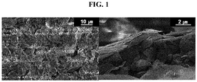
- FIG. 1 is a scanning electron microscopy (SEM) image of clay (talc) used in example 1
- FIG. 2 is an SEM image of silicon flakes finally obtained in example 1.
- a layered structure of raw material i.e., clay (talc) is found to include flakes stacked in 2 to 4 layers through covalent bond of silica and metal oxide, and when the stacked flakes are a unit structure, the thickness is 50 to 200 nm.
- silicon flakes synthesized in example 1 has a hyperporous structure.
- macropores having 100 to 150 nm size are uniformly formed on the surface of silicon flakes, and silicon flakes are stacked in 2 to 4 layers.
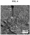
- FIG. 4 A smaller drawing in FIG. 4 is a high resolution image of FIG. 4 . Referring to FIG. 4 , it can be seen that mesopores and micropores are formed on the surface of silicon flakes.
- silicon flakes according to example 1 have a hyperporous structure.
- FIG. 7 is an SEM image of carbon-coated silicon flakes prepared in example 2, and a smaller drawing in FIG. 7 is a high resolution image of FIG. 7 .
- silicon flakes maintain a hyperporous structure well even after they are coated with a carbon layer.
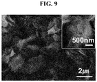
- FIG. 9 is an SEM image of clay (nanoclay) used in comparative example 1
- FIG. 10 is an SEM image of bulk silicon finally obtained in comparative example 1.
- a layered structure of raw material i.e., clay (nanoclay) is found to include nanosheets stacked through covalent bond of silica and metal oxide, and when the stacked nanosheets are a unit structure, the thickness is about 10 to 50 nm.
- silicon synthesized in comparative example 1 does not have an existing layered structure, and shows a structure of 3-dimensional (3D) bulk silicon primarily having 100 to 300 nm macropores.
- FIG. 11 is an SEM image of silicon flakes with added carbon compound prepared in comparative example 2, and a smaller drawing in FIG. 11 is a high resolution image of FIG. 11 .
- the structure of flakes is maintained on predetermined level, but during reduction reaction, the carbon compound hinders the reduction reaction, and as a result, the pore structure is not definite, and a non-uniform structure is formed.
- FIG. 13 is an SEM image of carbon-coated porous bulk silicon prepared in comparative example 3.
- a porous structure composed only of macropores is formed in bulk silicon with 3D structure, and a hyperporous structure is not found.
- silicon prepared from raw material i.e., clay (illite) shows a flake structure, but a hyperporous structure on the surface is absent.
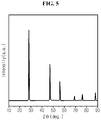
- FIG. 15 is an X-ray diffraction (XRD) graph of silicon flakes with no hyperporous structure prepared in comparative example 4.
- FIG. 16 is an SEM image of silicon flakes obtained in comparative example 5, and an inside figure in FIG. 16 is a high resolution image of FIG. 16 .
- silicon flakes synthesized under temperature condition of 400°C have a structure of flakes of the used clay (talc), but the pore structure is irregular and does not achieve a hyperporous structure.
- a general magnesium reduction reaction is accomplished when magnesium melts around the melting point of magnesium and reacts with silica, and magnesium does not fully participate in reaction at 400°C, failing to achieve full reduction of silicon flakes, and as a consequence, a hyperporous structure is not formed.
- FIG. 17 is an SEM image of silicon flakes obtained in comparative example 6.
- FIG. 17 A smaller drawing in FIG. 17 is a high resolution image of FIG. 17 .
- macropores are not formed on the surface of silicon flakes under reaction conditions of 650°C and 10 minutes, and a layer composed of mesopores and micropores covers the surface.
- reaction time 10 minutes, reaction is not fully made, and silicon flakes do not perfectly form a hyperporous structure.
- FIG. 30 is an SEM image of diatomite used in comparative example 7
- FIG. 31 is an SEM image of silicon flakes finally obtained in comparative example 7.
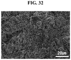
- FIG. 32 is an SEM image of slag used in comparative example 8
- FIG. 33 is an SEM image of silicon flakes finally obtained in comparative example 8.
- reaction time is 30 minutes, macropores structure starts to form, and due to reaction heat, a layer of silicon flakes delaminated from the stack structure of clay is formed.
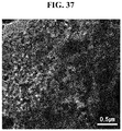
- FIG. 37 is a TEM image of silicon flakes having undergone thermal treatment reaction at 650°C for 6 hours. Referring to FIG. 37 , it can be seen that as the thermal treatment time increases, all the particles increase in size. This is thought to be aggregation typically appearing when subjected to reaction at high temperature for a long time, and one more point to note is a size reduction of macropores to very small size and consequential indefinite boundary as described previously. It may be caused by agglomeration of many layers of silicon flakes.
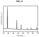
- the XRD equipment (D8 Advance, Bruker) was used to measure at 3kW X-ray power, 20kV measurement voltage, 50mA measurement current, and the measurement range between 10 and 90 degrees.
- a thin carbon layer is coated, but it is too small to be observed through XRD analysis, and referring to FIG. 12 , it can be seen that silicon and graphene oxide exist together.
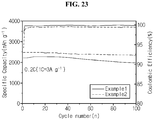
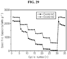
- charge/discharge capacity was measured at 25°C with .05C current and voltage ranging from 0.01 to 1.2 V, and discharge capacity and charge/discharge efficiency results are shown in FIGS. 18 to 22 .
- the half coin cells manufactured using silicon flakes and carbon-coated silicon flakes have the specific charge/discharge capacity of 2209/2383 and 2984/3216, and the initial charge/discharge efficiency of 92.67% and 92.77% respectively.
- the half coin cell manufactured using bulk silicon prepared from nanoclay has the specific charge/discharge capacity of 1772/2497, and the initial charge/discharge efficiency of 70.96%.
- the half coin cell manufactured using silicon flakes with added carbon compound had the specific charge/discharge capacity of 2027/2475, and the initial charge/discharge efficiency of 81.9%.
- the half coin cell manufactured using carbon-coated porous silicon prepared through a metal-assisted chemical etching method has the specific charge/discharge capacity of 2565/2886, and the initial charge/discharge efficiency of 88.88%.
- the half coin cell manufactured using silicon flakes with no hyperporous structure has the specific charge/discharge capacity of 1243/1381, and the initial charge/discharge efficiency of 90.05%.
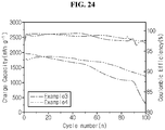
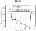
- charge/discharge capacity was measured at 25°C with .05C current and voltage ranging from 0.01 to 1.2 V, and discharge capacity and charge/discharge efficiency results are shown in FIG. 34 .
- the half coin cells manufactured using silicon flakes (example 1) and carbon-coated silicon flakes (example 2) have the specific charge/discharge capacity of 2209/2383 and 2984/3216, and the initial charge/discharge efficiency of 92.67% and 92.77%.
- the initial charge/discharge efficiency is considerably high compared to the case using bulk silicon and silicon flakes with no hyperporous structure, and further, it can be seen that they have higher initial charge/discharge efficiency than silicon flakes including carbon compound and carbon-coated porous silicon.
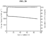
- the carbon-coated silicon prepared in examples 3 and 4 was used as a negative electrode active material, PAA/CMC was used as a binder, and carbon black was used as a conductive material.
- the negative electrode active material: binder: conductive material were mixed well in water at a weight ratio of 8: 1: 1, applied to a 18 ⁇ m thick Cu foil, and dried at 150°C to manufacture a negative electrode.
- the half coin cells manufactured using silicon flakes (example 1) and carbon-coated silicon flakes (example 2) as an active material have the cycle life of 89.0% and 94.6% in 100 charge/discharge cycles at the rate of 0.2 C respectively.
- life characteristics of the half coin cells manufactured using silicon flakes of examples 3 and 4 as an active material were evaluated in 100 charge/discharge cycles at the rate of 0.2 C. They have sufficiently good life characteristics compared to comparative examples.
- the life of the half coin cell using bulk silicon of comparative example 1 as an active material expired in 100 charge/discharge cycles at the rate of 0.2 C.
- the half coin cell manufactured using silicon flakes with added carbon compound has a rapid reduction in charge/discharge cycles at the rate of 0.2C, and has the cycle life of only 18.3% in 70 charge/discharge cycles at the rate of 0.5C.
- the life of the half coin cell manufactured using carbon-coated porous silicon expired in 100 charge/discharge cycles at the rate of 0.2C.
- the half coin cell manufactured using silicon flakes with no hyperporous structure has the cycle life of 71.74% in 90 charge/discharge cycles at the rate of 0.2C.
- the half coin cells manufactured using silicon flakes (example 1) and carbon-coated silicon flakes (example 2) show cycle characteristics of 100% and 95.97% in 50 charge/discharge cycles at 0.2 C rate, respectively.
- silicon synthesized from diatomite and Ferro-Si comparative example 9 showed life characteristics of 56.47% and 71.36% respectively.
- the cycle life was longer than the case using bulk silicon and silicon flakes with no hyperporous structure, and further, in the case of using carbon-coated silicon flakes, there is an effect on significantly improving the life characteristics compared to silicon flakes with added carbon compound.
- the half coin cells manufactured using silicon flakes (example 1) and carbon-coated silicon flakes (example 2) have the specific capacity of about 25 and 585 at 10 C rate.
- each specific capacity at 5 C is 134 and 958
- each silicon synthesized from diatomite of comparative example 7 and Ferro-Si of comparative example 8 is used, each specific capacity is 28 and 87 (unit of specific capacity: mAhg -1 ).
- the performance is also good in terms of rate characteristics, but when carbon-coated silicon flakes are used, it is much better in terms of rate characteristics.
- silicon flakes and carbon-coated silicon flakes according to an embodiment of the present disclosure have better initial efficiency, life characteristics, and rate characteristics than other silicon materials synthesized through Mg reduction.
- the silicon flakes according to an embodiment of the present disclosure can have greatly improved electrolyte solution impregnation characteristics through the hyperporous structure.
- Most of the porous silicon structures have pores on the surface only, while the silicon flakes according to an embodiment of the present disclosure have large macropores over the entire structure, bringing an electrolyte solution and an electrode material into uniform contact from the initial cycle, which helps improve the diffusion of lithium ions.
- the silicon flakes according to an embodiment of the present disclosure have various types of pores including macropores as well as mesopores and micropores, which is advantageous in terms of accommodating the volume expansion. According to earlier studies, volume expansion was reduced through porous structure, and 3D porous structure was proposed. Completely different from the earlier technology, the silicon flakes according to an embodiment of the present disclosure are applied as a silicon negative electrode active material with 2D porous structure.
- the silicon flakes according to an embodiment of the present disclosure exhibits superior reversible capacity at a high C rate despite a large particle size, which greatly improves electrolyte solution impregnation characteristics through the hyperporous structure, helping improve the diffusion of lithium ions, and thus it is advantageous in terms of accommodating the volume expansion.
- the reason why a material with 2D structure is more advantageous in volume expansion than 3D structure is that even under the same volume expansion, a material with 2D structure can maintain the structure better and a material with 3D structure changes the structure to 2D structure in many cycles. 2D structure expands in surface direction and vertical direction, and even though the same volume expansion is taken into account, an expansion rate in a real electrode is much smaller, so it is superior to the material of 3D structure expanding in all directions.
- FIG. 38 is a diagram of silicon flakes with hyperporous structure according to an embodiment of the present disclosure.
- the largest and round part is macropore, and pores disposed on the surface thereof are mesopore and micropore. That is, mesopores and micropores are formed on the frame surface of silicon flakes, and macropores are holes created inside of the silicon flakes frame, that is, in the frame itself.
Description
- The present disclosure relates to a negative electrode material comprising silicon flakes and a preparing method of silicon flakes.
- The present application claims the benefit of Korean Patent Application No.
10-2016-0104774 filed on August 18, 2016 - As the use of fossil fuels dramatically increases, it is required to use alternative energy and clean energy more and more, and in this circumstance, studies are made most intensively in the field of power generation and storage using electrochemistry.
- Currently, a typical example of electrochemical devices using electrochemical energy is secondary batteries, and the range of applications is gradually expanding.
- With the technology development and the increasing demand for mobile devices such as portable computers, mobile phones and cameras, the demand for secondary batteries as a source of energy is dramatically increasing at recent years, and among secondary batteries, lithium secondary batteries with high energy density and operating potential, a long cycle life and a low self-discharge rate have extensively been studied, and are commercialized and come into widespread use.
- In addition, with the increasing interest in environmental issue, many studies are being made on electric vehicles and hybrid electric vehicles that provide an alternative to cars using fossil fuels such as gasoline cars and diesel cars, known as one of the main causes of air pollution. Nickel/metal hydride secondary batteries are primarily used as a source of power for electric vehicles and hybrid electric vehicles, but lithium secondary batteries with high energy density and discharge voltage are intensively being studied and some manufacturers are commercializing products.
- Materials including graphite are widely used as a negative electrode (anode) active material of lithium secondary batteries. Materials including graphite have an average potential of about 0.2V (for Li/Li+) when disintercalating lithium, and during discharge, the potential changes relatively uniformly. By this reason, an advantage is a high and uniform battery voltage. However, graphite materials have an electrical capacity per unit mass as low as 372 mAh/g, but the capacity of graphite materials has been improved and now gets close to the theoretical capacity, so it is difficult to further increase the capacity.
- For higher capacity of lithium secondary batteries, many negative electrode active materials are being studied. Negative electrode active materials with high capacity include materials that form lithium-metal compounds, and for example, silicon or tin is expected to be a promising negative electrode active material. Particularly, silicon is an alloy type negative electrode active material having a theoretical capacity (4,200 mAh/g) that is at least about 10 times higher than graphite, and is today gaining attention as a negative electrode active material of lithium secondary batteries.
- However, silicon has a large volume change (∼300%) during charge/discharge, causing the mechanical contact between materials to break, resulting in spalling, and as a consequence, ionic conductivity and electrical conductivity reduces, and life characteristics tend to reduce sharply in real situation.
- Accordingly, to solve the problem with volume change of Si, a bottom-up approach to design/synthesize Si with nanostructure is recently receiving much attention, but its downside is an intricate production process, low yield and high production costs, making commercialization difficult.
- To apply silicon to lithium secondary batteries, there is an urgent need for development of technology to improve life characteristics and rate characteristics and minimize volume changes during charge/discharge.
-
WO 2015/082920 A1 discloses a method for the manufacture of electrodes for metal ion batteries, the method comprising sintering porous silicon-containing particles at a temperature of 500 to 1200 °C and in an oxygen-free atmosphere. - Therefore, the present disclosure is aimed at solving the problem of the related art and the technical problem that has been long requested.
- After in-depth studies and various experiments, the inventors completed the present disclosure based on the findings that synthesis of flake shaped silicon with hyperporous structure from low-priced clay using a metal reducing agent leads to production cost reduction and simple production process, and fabrication of a lithium secondary battery using the resulting silicon flakes as a negative electrode active material has effects in buffering volume expansion during charge/discharge and improving life characteristics and rate characteristics.
- To achieve this object, a negative electrode material of the present disclosure, as defined in
claim 1, includes, as an active material, silicon flakes with hyperporous structure, represented by the following chemical formula 1:
- In the formula,

- A is an impurity selected from the group consisting of Al2O3, MgO, SiO2, GeO2, Fe2O3, CaO, TiO2, Na2O K2O, CuO, ZnO, NiO, Zr2O3, Cr2O3 and BaO.
- Here, the x is a weight ratio, and the 'silicon flake' specifically refers to a plate structure or substantial plate structure in which silicon atoms having 2-dimensional (2D) crystal shape or tetrahedral crystal shape are periodically arranged in 2 dimensions.
- Furthermore, the 'hyperporous structure' refers to a structure in which macropores, mesopores and micropores classified based on the pore size are formed together.
- The silicon flakes with hyperporous structure have a hyperporous structure including macropores having the pore size in the range of greater than 50 nm to 500 nm, mesopores having the pore size of greater than 2 nm to 50 nm, and micropores having the pore size of 0.5 nm to 2 nm.
- The hyperporous structure is formed when the silicon flakes of the present disclosure are synthesized, and as described below, the silicon flakes of the present disclosure are synthesized by a metallothermic reduction method that thermally treats clay and a metal reducing agent. In this case, first, mesopores and micropores are formed together on the surface of clay through surface reaction of clay and a metal reducing agent, and macropores are not formed. Subsequently, as the reaction progresses, the metal reducing agent penetrated into the clay through the mesopores and micropores formed on the surface causes an internal reduction reaction to take place, metal oxide produced inside plays a role in forming macropores later and macropores are formed at the position of the metal oxide through subsequent post-treatment for removing the metal oxide, completing a hyperporous structure.
- When the silicon flakes with hyperporous structure are used as a negative electrode active material, volume expansion of silicon can be alleviated by the hyperporous structure during charge/discharge, and there is an effect on the marked improvements in life characteristics and rate characteristics appearing by increasing the contact area with an electrolyte and reducing the movement distance of lithium ions.
- To exert the intended effects more effectively, and achieve high capacity per volume, the pores of the silicon flakes with hyperporous structure may have an average pore diameter of 100 nm to 150 nm, and a porosity of 10% to 50%, specifically 10% to 30%, based on the total volume.
- Furthermore, the BET surface area of the silicon flakes may be 70 m2/g to 250 m2/g. Specifically, the BET surface area may be 120m2/g to 210 m2/g, and more specifically, 150m2/g to 190 m2/g.
- Here, the porosity was roughly calculated based on the total pore volume and tap density, and the BET surface area was measured by N2 adsorption-desorption isotherm measurement using Micromeritics ASAP 2020 instrument. In addition, the average pore diameter was calculated by applying BJH (Barrett, Johner and Halenda) equation to the result.
- Furthermore, the silicon flakes may have a thickness of 20 to 100 nm, and a size of 200 nm to 50 µm, but is not limited thereto.
- However, when the silicon flakes are thin enough to satisfy the range and large in size, it is more preferred because the movement distance of lithium ions can be effectively reduced and impregnation of an electrolyte is easy. Specifically, the silicon flakes may have a thickness of 30 to 50 nm, and a size of 1 µm to 5 µm.
- When a stack of silicon flakes is a unit (one), one flake may be formed, but 2 to 6 flakes, specifically 2 to 4 flakes may be stacked according to the synthesis conditions for forming silicon flakes, but is not limited thereto. When silicon flakes are used as a negative electrode active material of a lithium secondary battery, two or more silicon flakes stacked may be used. Accordingly, it is obvious that 'including silicon flakes as an active material' encompasses a stack of one or more silicon flakes when a silicon flake shaped material is a unit.
- Meanwhile, when the silicon flakes according to the present disclosure are used as an active material, carbon coating may be performed to increase electronic conductivity and improve the rate characteristics.
- In this instance, the carbon coating may be carried out as an additional process in the preparation of the silicon flakes, and a detailed description is provided in the following preparing method.
- The carbon coating may have a thickness of 1 to 100 nm, specifically 3 to 30 nm, and more specifically, 5 nm to 15nm.
- When the range is satisfied, rate characteristics sought to obtain from the carbon coating are improved and uniform carbon coating is formed, and as a result, electrochemical performance is improved, and a suitable amount of silicon for achieving high capacity to the total volume is ensured, thereby preventing the capacity reduction problem.
- Meanwhile, the present disclosure also provides a preparing method of the silicon flakes, as defined in claim 9, including:
- i) thermally treating a mixture of clay and a metal reducing agent at 500°C to 800°C for 30 minutes to 6 hours;
- ii) adding the thermally treated mixture to an acidic solution and stirring; and
- iii) obtaining silicon flakes with hyperporous structure from the stirred result.
- According to the method, when the uniform mixture of the clay and the metal reducing agent is subjected to reaction around the melting point of the metal reducing agent, the metal reducing agent starts to melt, causing reduction reaction to take place on the clay surface, so that silica in the outermost layer is reduced to silicon, releasing an excessive amount of heat. The released heat is transferred to a lower layer composed of metal oxide in the clay, and the metal oxide acts as a negative catalyst and a heat scavenger to mitigate the excessive amount of heat generated from the reduction reaction. Subsequently, macropores are formed at the position of the metal oxide through acidic solution post-treatment to remove the metal oxide, and silicon flakes with hyperporous structure are obtained together with the existing mesopores and micropores.
- In this instance, the clay used to obtain the silicon flakes may have a layered structure, and specifically, may have a structure corresponding to a plate structure corresponding to the shape of the silicon flakes.
- As described above, high-purity silicon with the purity of 90wt% or higher, specifically 95wt% or higher can be obtained from redundant and low-priced clay, and by the preparing method, it is thus very good in aspects of production costs and process.
- Specifically, the clay includes, but is not limited to, any clay having a layered structure, and may be clay including a mineral selected from the group consisting of montmorillonite, mica, talc, and their combination as a clay mineral, and specifically, talc.
- The type of metal oxide may change depending on the type of mineral included in the clay, and accordingly, the metal reducing agent for obtaining silicon by reducing silica included in the clay may be the same metal as metal oxide except silicon oxide included in the clay, and specifically, may be a metal selected from the group consisting of Al, Mg, Ge, Fe, Ca, Ti, Cu, Zn, Ni, Zr, Cr, Ba and their combination, specifically, Al or Mg. The metal reducing agent may be, specifically, in the form of powder, but is not limited thereto.
- In the i) process, a mix ratio between the clay and the metal reducing agent may be such that a mole ratio between oxygen of silicon oxide included in the clay and the metal reducing agent is from 1 : 0.5 to 1 : 2.
- When the amount of metal reducing agent is too much beyond the range, the metal reducing agent may be rather an impurity, and when the amount of metal reducing agent is too little, silica that is not reduced to silicon may remain behind, unfavorably resulting in low purity.
- The mixture of the clay and the metal reducing agent goes through thermal treatment, and by the thermal treatment, silica included in the clay is reduced into silicon flakes, and the metal reducing agent is oxidized. This process can be, as an example, represented by the following chemical formula:
(SiO2)x(MgO)y + 2xMg → xSi + (2x+y)MgO
(SiO2)x(Al2O3)y + 4/3xAl → xSi + (2/3x+y)MgO
- The i) thermal treatment process for reduction reaction is performed at 500°C to 800°C for 30 minutes to 6 hours, and specifically, may be performed at 600°C to 800°C for 1 hour to 3 hours.
- When the temperature is too low or the time is short beyond the range, reduction of silica included in the clay is insufficient, failing to obtain silicon flakes, and when the temperature is too high or the time is long, a hyperporous structure of desired shape cannot be obtained due to crystal structure rearrangement.
- Furthermore, the thermal treatment may be performed under atmosphere including inert gas, and specifically, may be performed under atmosphere including gas selected from the group consisting of nitrogen gas, argon gas, neon gas, helium gas and their combination, specifically under argon gas atmosphere.
- The metal reducing agent oxidized in the process produces oxide which acts as an impurity, and only the reduced silicon flakes can be obtained with high purity by removing the impurity by stirring with an acidic solution in the subsequent ii) process.
- In this instance, the ii) stirring process in the acidic solution may include stirring in a first acidic solution; and stirring in a second acidic solution in a sequential order.
- The double stirring in the acidic solution is for completely removing metal oxide existing in the mixture having undergone reduction reaction through thermal treatment and unreacted silica residual.
- Specifically, the acidic solution used to remove metal oxide and silica may be selected from the group consisting of hydrochloric acid, nitric acid, sulfuric acid, phosphoric acid, hydrofluoric acid, perchloric acid, chloric acid, chlorous acid, hypochlorous acid, iodic acid, and their combination. That is, each of the first acidic solution and the second acidic solution may be independently selected from the group consisting of hydrochloric acid, nitric acid, sulfuric acid, phosphoric acid, hydrofluoric acid, perchloric acid, chloric acid, chlorous acid, hypochlorous acid, iodic acid, and their combination. More specifically, the first acidic solution may be hydrochloric acid, and the second acidic solution may be hydrofluoric acid. The hydrochloric acid plays a role in dissolving metal oxide, and the hydrofluoric acid plays a role in dissolving silica.
- The stirring process with the acidic solution may be appropriately determined based on an amount of remaining impurities, and specifically, may be performed at 24°C to 40°C for 5 minutes to 5 hours, and when the first acidic solution is hydrochloric acid, the stirring time with the first acidic solution may be specifically 2 hours to 5 hours at 30°C to 40°C, and when the second acidic solution is hydrofluoric acid, the stirring time with the second acidic solution may be 5 minutes to 30 minutes at room temperature.
- The impurity-free material yields silicon flakes with hyperporous structure from the stirred result in the iii) process. A method for obtaining or separating silicon flakes with hyperporous structure is not limited to a particular type, but for example, may be performed through filtering or a centrifugal separator.
- A method for obtaining the result included in the solution using the centrifugal separator is known in the art, and specifically, the filtering may be a method through a vacuum filter, and a method for obtaining the result through the vacuum filter may include appropriately setting up the vacuum filter, and pouring the stirred solution into a vacuum filter container to separate the acidic solution and other solvents from silicon flakes.
- In this instance, the method for obtaining using the centrifugal separator has problems with a minimum solvent volume of 200ml or more, and incomplete separation in the case of a neutral solution with the acidic solution, and specifically, it is more desirable to synthesize silicon flakes with hyperporous structure from the stirred material through the filtering.
- Meanwhile, the preparing method of the silicon flakes may further include:
iv) thermally treating with providing carbon containing gas to the obtained silicon flakes. - Through this process, carbon-coated silicon flakes can be obtained.
- In this instance, the carbon containing gas may be selected from acetylene gas, ethylene gas, propylene gas, methane gas, ethane gas and their combination, and specifically, may be acetylene gas.
- Furthermore, the iv) thermal treatment process for coating with carbon through carbon containing gas may be performed at 500°C to 1,000°C for 1 minute to 30 minutes, and specifically, for 1 minute to 10 minutes.
- When the process is performed at too low temperature or for too short time beyond the range, a desired degree of carbon coating is not achieved, and when the process is performed at too high temperature or for too long time, the crystal structure and hyperporous structure of silicon flakes are affected, and the structure may be changed to a structure that forms a complex with silicon flakes, not a structure that coats with carbon.
- When silicon flakes are coated with carbon using carbon containing gas at the end of preparation, carbon has connectivity while not clogging the pores of silicon, so that an electron movement path is effectively formed and silicon flakes are coated in gas state, achieving uniform coating on the surface of silicon flakes, and thus, when reaction is induced with an addition of a carbon compound together in the course of preparation, a complex of silicon and the carbon compound is formed, and as the carbon compound forms a complex with silicon, the carbon compound may hamper the formation of pores, and silicon carbide may be formed due to an excessive amount of heat generated during metallothermic reduction reaction, but because silicon carbide is electrochemically inactive, it is better in aspects of structural maintenance of silicon flakes, uniform carbon coating and prevention of loss of active material.
- The present disclosure also provides a negative electrode including the negative electrode material and a secondary battery including the negative electrode.
- The secondary battery according to the present disclosure generally includes a positive electrode, a negative electrode, a separator and a lithium salt containing non-aqueous electrolyte. Accordingly, components that make up the lithium secondary battery other than the negative electrode material according to the present disclosure described above are described below.
- The positive electrode is manufactured by applying a mixture of a positive electrode active material, a conductive material and a binder to a positive electrode current collector and drying it, and a filler may be added to the mixture if necessary.
- The positive electrode active material includes, but is not limited to, layered compound such as lithium cobalt oxide (LiCoO2), lithium nickel oxide (LiNiO2) or compounds with one or more transition metal substitution; lithium manganese oxide of chemical formula Li1+yMn2-yO4 (in which y is 0 ∼ 0.33) such as LiMnO3, LiMn2O3, LiMnO2; lithium copper oxide (Li2CuO2); vanadium oxide such as LiV3O8, LiFe3O4, V2O5, Cu2V2O7; Ni-site lithium nickel oxide represented by chemical formula LiNi1-yMyO2 (in which M = Co, Mn, Al, Cu, Fe, Mg, B or Ga, y = 0.01 ∼ 0.3); lithium manganese composite oxide represented by chemical formula LiMn2-yMyO2 (in which M = Co, Ni, Fe, Cr, Zn or Ta, y = 0.01 ∼ 0.1) or Li2Mn3MO8 (in which M = Fe, Co, Ni, Cu or Zn); LiMn2O4 with partial substitution of alkali earth metal ion for Li in chemical formula; disulfide compound; Fe2(MoO4)3.
- The conductive material is generally present in an amount of 1 to 50 wt% based on the total weight of the mixture including the positive electrode active material. The conductive material is not limited to any particular type if it has conductivity while not causing a chemical change to the corresponding battery, and for example, graphite such as graphene, graphite pellet, natural graphite or artificial graphite; carbon black such as carbon black, acetylene black, ketjen black, channel black, furnace black, lamp black and thermal black; carbon fiber such as CNT or conductive fiber such as metal fiber; metal powder of fluorinated carbon, aluminum, nickel powder; conductive whisker of zinc oxide and potassium titanate; conductive metal oxide such as titanium oxide; conductive material such as polyphenylene derives.
- The binder is a component that assists in binding the active material to the conductive material and to the current collector, and is generally present in an amount of 1 to 50 wt% based on the total weight of the mixture including the positive electrode active material. Examples of the binder include polyvinylidene fluoride, polyvinyl alcohol, polyacrylic acid (PAA), carboxymethyl cellulose (CMC), starch, hydroxypropyl cellulose, regenerated cellulose, polyvinylpyrrolidone, tetrafluoroethylene, polyethylene, polypropylene, ethylene-propylene-diene ter polymer (EPDM), sulfonated EPDM, styrenebutadiene rubber, fluorine rubber, and a variety of copolymers.
- The filler is a component that inhibits the expansion of the positive electrode and is optionally used, and the filler is not limited to any particular type if it is a fibrous material while not causing a chemical change to the corresponding battery, and for example, includes olefin-based polymer such as polyethylene and polypropylene; fibrous material such as glass fiber and carbon fiber.
- The positive electrode current collector is formed 3 to 500 µm in thickness. The positive electrode current collector is not limited to any particular type if it has high conductivity while not causing a chemical change to the corresponding battery, and for example, includes stainless steel, aluminum, nickel, titanium, sintered carbon, or aluminum or stainless steel surface treated with carbon, nickel, titanium, and silver. The current collector may have fine surface texture to increase the adhesion of the positive electrode active material, and may come in various types including films, sheets, foils, nets, porous materials, foams, and nonwovens.
- The negative electrode is manufactured by binding a negative electrode material, i.e., a mixture of an active material, a conductive material and a binder to a negative electrode current collector according to common methods known in the art, and plays a role in intercalating and deintercalating lithium ions in the same way as the positive electrode.
- In addition to silicon flakes defined in the present disclosure, the negative electrode active material may further include carbon material composed only of carbon atoms with completely crystalized structure (ordered structure) by thermal treatment at the temperature of 2000°C or above, for example, carbon black such as natural graphite, artificial graphite, channel black, acetylene black, ketjen black and furnace black, Kish graphite (KG), SFG series (SFG-6, SFG-15, etc.), highly oriented pyrolytic graphite, Mesophase pitch based carbon fiber (MPCF), MCMB series (MCMB 2800, MCMB 2700,
MCMB 2500, etc.). - The negative electrode current collector is formed 3 to 500 µm in thickness. The negative electrode current collector is not limited to any particular type if it has conductivity while not causing a chemical change to the corresponding battery, and for example, includes copper, stainless steel, aluminum, nickel, titanium, sintered carbon, copper or stainless steel surface treated with carbon, nickel, titanium, and silver, and aluminum-cadmium alloy. Furthermore, similar to the positive electrode current collector, the negative electrode current collector may have fine surface texture to enhance the bond strength of the negative electrode active material, and may come in various types including films, sheets, foils, nets, porous materials, foams, and nonwovens.
- The negative electrode is manufactured by applying a mixture of the negative electrode active material, the conductive material and the binder to the negative electrode current collector and drying it, and a filler may be added to the mixture if necessary. In this instance, the type and amount of the conductive material, the binder and the filler used may be applied by referring to the description of the positive electrode.
- The separator is interposed between the positive electrode and the negative electrode, and includes an insulating thin film with high ionic permittivity and mechanical strength. Generally, the separator has a pore diameter of 0.01 ∼ 10 µm, and a thickness of 5 ∼ 300 µm. The separator includes, for example, chemical-resistant and hydrophobic olefin-based polymer such as polypropylene; sheets or nonwovens made of glass fiber or polyethylene. When a solid electrolyte such as polymer is used as the electrolyte, the solid electrolyte may serve as the separator.
- The lithium salt containing non-aqueous electrolyte includes a non-aqueous electrolyte solution and a lithium salt, and the non-aqueous electrolyte solution includes a non-aqueous organic solvent, an organic solid electrolyte, and an inorganic solid electrolyte.
- The organic solid electrolyte includes, for example, polyethylene derivatives, polyethylene oxide derivatives, polypropylene oxide derivatives, phosphoric acid ester polymer, poly agitation lysine, polyester sulfide, polyvinyl alcohol, polyvinylidene fluoride, and polymer including ionic dissociable group.
- The inorganic solid electrolyte includes, for example, nitride, halogenide, and sulphate of Li such as Li3N, LiI, Li5NI2, Li3N-LiI-LiOH, LiSiO4, LiSiO4-LiI-LiOH, Li2SiS3, Li4SiO4, Li4SiO4-LiI-LiOH, Li3PO4-Li2S-SiS2.
- The lithium salt is a material that is apt to dissolve in the non-aqueous electrolyte, and includes, for example, LiCl, LiBr, LiI, LiClO4, LiBF4, LiB10Cl10, LiPF6, LiCF3SO3, LiCF3CO2, LiAsF6, LiSbF6, LiAlCl4, CH3SO3Li, CF3SO3Li, (CF3SO2)2NLi, chloroborane lithium, lithium lower aliphatic carboxylate, lithium tetraphenylborate, and imide.
- Furthermore, to improve the charging/discharging characteristics and flame retardancy, for example, pyridine, triethylphosphite, triethanolamine, cyclic ether, ethylene diamine, n-glyme, triamide hexaphosphate, nitrobenzene derivatives, sulfur, quinone imine dye, N-substituted oxazolidinone, N,N-substituted imidazolidine, ethylene glycol dialkyl ether, ammonium salts, pyrrole, 2-methoxy ethanol, and aluminum trichloride may be added to the electrolyte solution. In some cases, to give non-combustibility, a halogen containing solvent such as carbon tetrachloride and trifluoroethylene may be further included, and to improve the preservation at high temperature, carbon dioxide gas may be further included.
- As described hereinabove, the negative electrode material according to the present disclosure includes silicon flakes with hyperporous structure synthesized from low-priced clay using a metal reducing agent, leading to production cost reduction and simple production process due to the synthesis of the silicon flakes, and when a lithium secondary battery is manufactured using the same, pores with various sizes alleviate the volume expansion of silicon, and despite the micrometer size of silicon, the hyperporous structure increases the contact area with an electrolyte and reduces the movement distance of lithium ions compared to conventional bulk silicon, thereby providing an improvement effect of life characteristics and rate characteristics.
-
-
FIG. 1 is a scanning electron microscopy (SEM) image of clay (talc) used in example 1. -
FIG. 2 is an SEM image of silicon flakes prepared in example 1. -
FIG. 3 is a transmission electron microscopy (TEM) image of silicon flakes prepared in example 1. -
FIG. 4 is a high resolution TEM image of silicon flakes prepared in example 1. -
FIG. 5 is an X-ray diffraction (XRD) graph of silicon flakes prepared in example 1. -
FIG. 6 is a TEM image showing a pore formation process of silicon flakes prepared in example 1 as a function of reaction time. -
FIG. 7 is an SEM image of carbon-coated silicon flakes prepared in example 2. -
FIG. 8 is an XRD graph of carbon-coated silicon flakes prepared in example 2. -
FIG. 9 is an SEM image of clay (nanoclay) used in comparative example 1. -
FIG. 10 is an SEM image of porous silicon prepared in comparative example 1. -
FIG. 11 is an SEM image of silicon flakes prepared with an addition of carbon compound in comparative example 2. -
FIG. 12 is an XRD graph of silicon flakes prepared with an addition of carbon compound in comparative example 2. -
FIG. 13 is an SEM image of carbon-coated porous bulk silicon prepared in comparative example 3. -
FIG. 14 is an SEM image of silicon flakes with no hyperporous structure prepared in comparative example 4. -
FIG. 15 is an XRD graph of silicon flakes with no hyperporous structure prepared in comparative example 4. -
FIG. 16 is an SEM image of silicon flakes prepared in comparative example 5. -
FIG. 17 is an SEM image of silicon flakes prepared in comparative example 6. -
FIG. 18 is an initial charge/discharge graph of coin cell fabricated in experimental example 4 using silicon flakes of example 1 and example 2 as an active material. -
FIG. 19 is an initial charge/discharge graph of coin cell fabricated in experimental example 4 using bulk silicon of comparative example 1 as an active material. -
FIG. 20 is an initial charge/discharge graph of coin cell fabricated in experimental example 4 using silicon flakes with added carbon compound of comparative example 2 as an active material. -
FIG. 21 is an initial charge/discharge graph of coin cell fabricated in experimental example 4 using carbon-coated porous bulk silicon of comparative example 3 as an active material. -
FIG. 22 is an initial charge/discharge graph of coin cell fabricated in experimental example 4 using silicon flakes with no hyperporous structure of comparative example 4 as an active material. -
FIG. 23 is a graph showing charge/discharge life characteristics of coin cell fabricated in experimental example 5 using silicon flakes of example 1 and example 2 as an active material. -
FIG. 24 is a graph showing charge/discharge life characteristics of coin cell fabricated in experimental example 5 using silicon flakes coated with carbon at different thicknesses of examples 3 and 4 as an active material. -
FIG. 25 is a graph showing charge/discharge life characteristics of coin cell fabricated in experimental example 5 using bulk silicon of comparative example 1 as an active material. -
FIG. 26 is a graph showing charge/discharge life characteristics of coin cell fabricated in experimental example 5 using silicon flakes with added carbon compound of comparative example 2 as an active material. -
FIG. 27 is a graph showing charge/discharge life characteristics of coin cell fabricated in experimental example 5 using carbon-coated porous bulk silicon of comparative example 3 as an active material. -
FIG. 28 is a graph showing charge/discharge life characteristics of coin cell fabricated in experimental example 5 using silicon flakes with no hyperporous structure of comparative example 4 as an active material. -
FIG. 29 is a graph showing charge/discharge characteristics as a function of C-rate for coin cell fabricated in experimental example 6 using silicon flakes of example 1 and example 2 as an active material. -
FIG. 30 is an SEM image of diatomite used in comparative example 7. -
FIG. 31 is an SEM image of silicon flakes finally obtained in comparative example 7. -
FIG. 32 is an SEM image of slag used in comparative example 8. -
FIG. 33 is an SEM image of silicon flakes finally obtained in comparative example 8. -
FIG. 34 is an initial charge/discharge graph of coin cell fabricated in experimental example 4 using each silicon material of example 1, example 2, comparative example 7, and comparative example 8 as an active material. -
FIG. 35 is a graph showing charge/discharge life characteristics of coin cell fabricated in experimental example 5 using silicon material of example 1, example 2, comparative example 7, and comparative example 8 as an active material. -
FIG. 36 is a graph showing charge/discharge characteristics as a function of C-rate for coin cell fabricated in experimental example 6 using silicon material of example 1, example 2, comparative example 7, and comparative example 8 as an active material. -
FIG. 37 is a TEM image of silicon flakes having undergone thermal treatment reaction of 650°C for 6 hours. -
FIG. 38 is a diagram of silicon flakes with hyperporous structure according to an embodiment of the present disclosure. - Hereinafter, the embodiments/examples are described to explain the present disclosure in more detail, but the following embodiments/examples are provided for illustration only, and the scope of the present disclosure is not limited thereto.
- 1g of clay (talc) was mixed with 0.7g of magnesium while milling uniformly using a mortar. The uniformly mixed mixture was put into a reaction container, and heated in argon atmosphere at 650°C for 3 hours to drive reduction reaction. The silicon flakes having undergone reaction were added to 200mL of 0.5M HCL aqueous solution and mixed at 35°C for 3 hours to remove magnesium oxide and other impurities. Removal of silica remaining after reaction was carried out by mixing silicon flakes with 0.1 to 5% of hydrofluoric acid for 5 to 30 minutes. Finally, silicon flakes with hyperporous structure were synthesized through a vacuum filter.
- Acetylene gas was introduced to silicon flakes synthesized in example 1 in 900°C argon atmosphere for 3 minutes to drive reaction. After naturally cooling to room temperature, finally, silicon flakes coated with carbon 9 nm in thickness were synthesized.
- Silicon flakes were synthesized in the same way as example 2 except that the thickness of carbon was 5 nm.
- Silicon flakes were synthesized in the same way as example 2 except that the thickness of carbon coated was 15 nm.
- The same process was performed except the type of clay used in synthesis example of silicon flakes. That is, clay used in comparative example 1 was nanoclay.
- Silicon composite including graphene oxide was obtained in the same way as example 1 except that reaction took place with an addition of 0.05g of carbon compound to 1 g of clay.
- 50g of bulk silicon was added to 100 mL of mixed solution of 40mM of CuSO4 with 5M HF and stirred at 50°C for 12 hours. After reaction, porous silicon including macropores was filtered out through a filter, and remaining Cu metal was removed by stirring in 50 mL of nitric acid solution at 50°C for 3 hours. Acetylene gas was introduced to the porous silicon in 900°C argon atmosphere for 28 minutes to drive reaction. After naturally cooling to room temperature, finally, porous silicon coated with 15wt% of carbon was synthesized.
- Silicon flakes were synthesized in the same way as example 1 except that the type of clay used was illite.
- Silicon flakes were synthesized in the same way as example 1 except that the reduction reaction temperature was 400°C.
- Silicon flakes were synthesized in the same way as example 1 except that the reduction reaction time was 10 minutes.
- Silicon flakes were synthesized by the same method as example 1 except that diatomite was used instead of clay (talc).
- Silicon flakes were synthesized by the same method as example 1 except that slag was used instead of clay (talc). In this instance, the used slag is also called iron slag, and its composition was CaO (43.3 wt%), SiO2 (34.5 wt%), Al2O3 (13.3 wt%), MgO (3.6 wt%), TiO2 (1.7 wt%), and Fe2O3 (1.1 wt%).
- For evaluation of appearance, SEM image and/or TEM image of clay used in examples 1 and 2 and comparative examples 1 to 6 and silicon flakes or bulk silicon prepared using the same are shown in
FIGS. 1 to 4 ,7 ,9 to 11 ,13 ,14 ,16 and17 . - Specifically,
FIG. 1 is a scanning electron microscopy (SEM) image of clay (talc) used in example 1, andFIG. 2 is an SEM image of silicon flakes finally obtained in example 1. - Referring to
FIG. 1 , a layered structure of raw material, i.e., clay (talc) is found to include flakes stacked in 2 to 4 layers through covalent bond of silica and metal oxide, and when the stacked flakes are a unit structure, the thickness is 50 to 200 nm. - Referring to
FIG. 2 , it can be seen that silicon flakes synthesized in example 1 has a hyperporous structure. - Furthermore, to understand the structure of silicon flakes finally obtained in example 1 better, a TEM image was taken and is shown in
FIG. 3 . - Referring to
FIG. 3 , it can be seen that macropores having 100 to 150 nm size are uniformly formed on the surface of silicon flakes, and silicon flakes are stacked in 2 to 4 layers. - A smaller drawing in
FIG. 4 is a high resolution image ofFIG. 4 . Referring toFIG. 4 , it can be seen that mesopores and micropores are formed on the surface of silicon flakes. - That is, analyzing
FIGS. 3 and4 together, it can be seen that silicon flakes according to example 1 have a hyperporous structure. - Furthermore,
FIG. 7 is an SEM image of carbon-coated silicon flakes prepared in example 2, and a smaller drawing inFIG. 7 is a high resolution image ofFIG. 7 . - Referring to
FIG. 7 , it can be seen that silicon flakes maintain a hyperporous structure well even after they are coated with a carbon layer. - Meanwhile,
FIG. 9 is an SEM image of clay (nanoclay) used in comparative example 1, andFIG. 10 is an SEM image of bulk silicon finally obtained in comparative example 1. - Referring to
FIG. 9 , a layered structure of raw material, i.e., clay (nanoclay) is found to include nanosheets stacked through covalent bond of silica and metal oxide, and when the stacked nanosheets are a unit structure, the thickness is about 10 to 50 nm. - In contrast, referring to
FIG. 10 , it can be seen that silicon synthesized in comparative example 1 does not have an existing layered structure, and shows a structure of 3-dimensional (3D) bulk silicon primarily having 100 to 300 nm macropores. - In the case of nanoclay, because metal oxide (i.e., aluminum oxide) inside cannot act as a negative catalyst (heat scavenger), an excessive amount of heat generated during reduction reaction is fully transmitted to the structure, and nanoclays of small size are agglomerated. Furthermore, 100 to 300nm macropores formed by removing MgO produced as a result of reduction are all that is formed, and accordingly, there is no hyperporous structure. For this reason, obviously, an existing layered structure or a layered structure such as silicon flakes cannot be maintained.
-
FIG. 11 is an SEM image of silicon flakes with added carbon compound prepared in comparative example 2, and a smaller drawing inFIG. 11 is a high resolution image ofFIG. 11 . - Referring to
FIG. 11 , in the case of silicon flakes synthesized with an addition of carbon compound, the structure of flakes is maintained on predetermined level, but during reduction reaction, the carbon compound hinders the reduction reaction, and as a result, the pore structure is not definite, and a non-uniform structure is formed. -
FIG. 13 is an SEM image of carbon-coated porous bulk silicon prepared in comparative example 3. - Referring to
FIG. 13 , a porous structure composed only of macropores is formed in bulk silicon with 3D structure, and a hyperporous structure is not found. - Further, to understand the structure of silicon flakes finally obtained in comparative example 4 better, an SEM image was taken and is shown in
FIG. 14 . - Referring to
FIG. 14 , silicon prepared from raw material, i.e., clay (illite) shows a flake structure, but a hyperporous structure on the surface is absent. -
FIG. 15 is an X-ray diffraction (XRD) graph of silicon flakes with no hyperporous structure prepared in comparative example 4. - Furthermore,
FIG. 16 is an SEM image of silicon flakes obtained in comparative example 5, and an inside figure inFIG. 16 is a high resolution image ofFIG. 16 . - Referring to
FIG. 16 , silicon flakes synthesized under temperature condition of 400°C have a structure of flakes of the used clay (talc), but the pore structure is irregular and does not achieve a hyperporous structure. - A general magnesium reduction reaction is accomplished when magnesium melts around the melting point of magnesium and reacts with silica, and magnesium does not fully participate in reaction at 400°C, failing to achieve full reduction of silicon flakes, and as a consequence, a hyperporous structure is not formed.
-
FIG. 17 is an SEM image of silicon flakes obtained in comparative example 6. - A smaller drawing in
FIG. 17 is a high resolution image ofFIG. 17 . Referring toFIG. 17 , it can be seen that macropores are not formed on the surface of silicon flakes under reaction conditions of 650°C and 10 minutes, and a layer composed of mesopores and micropores covers the surface. When the reaction time is 10 minutes, reaction is not fully made, and silicon flakes do not perfectly form a hyperporous structure. - That is, analyzing
FIGS. 16 and17 together, the synthesis conditions including reaction temperature and reaction time applied to example 1 are found reasonable. - For evaluation of appearance, SEM images of diatomite and slag used in comparative examples 7 and 8, and silicon flakes prepared using the same are shown in
FIGS. 30 to 33 . - Specifically,
FIG. 30 is an SEM image of diatomite used in comparative example 7, andFIG. 31 is an SEM image of silicon flakes finally obtained in comparative example 7. - Furthermore,
FIG. 32 is an SEM image of slag used in comparative example 8, andFIG. 33 is an SEM image of silicon flakes finally obtained in comparative example 8. - For silicon flakes prepared using talc for clay, compared to
FIG. 2 in which porous silicon of 2D structure was synthesized, in comparative example 7, porous silicon of 3D structure was synthesized, and in comparative example 8, mesoporous silicon particles having 500nm size were synthesized and a hyperporous structure was not formed. <Experimental example 2> - To understand the pore structure formation process of silicon flakes finally obtained in example 1 as a function of reaction time better, a TEM image was taken and is shown in
FIG. 6 . - Referring to
FIG. 6 , when the reaction time is 10 minutes, macropores structure of the silicon flakes was hardly observed, and the entire surface was composed of mesopores. It can be also seen that the thickness is more than the level of clay. Additionally, it can be seen that crystallinity of silicon reduces. - When the reaction time is 30 minutes, macropores structure starts to form, and due to reaction heat, a layer of silicon flakes delaminated from the stack structure of clay is formed.
- Furthermore, it can be seen that 50 to 70 % of the surface of silicon flakes is composed of mesopores, and crystallinity increases.
- When the reaction time is 1 hour, macropores have a more uniform size, and judging from the observation of overlapping macropores, it can be seen that delaminated silicon flakes start to be stacked in 2 to 3 layers.
- Furthermore, it can be seen that 10 to 30 % of the surface of silicon flakes is composed of mesopores, and crystallinity increases.
- When the reaction time is 3 hours, macropores have slightly smaller size, and a stack of 3 to 4 layers is observed.
- Furthermore, the mesoporous structure on the surface of silicon flakes disappears, and a frame of dense structure is observed.
- In conclusion, analyzing the TEM image of
FIG. 6 together, an excessive amount of mesopores are formed on the surface by a metal reducing agent at the initial time of reaction, and as the time passes, the reaction proceeds into the clay, making delamination and macropores structure more clear, and when the reaction time is longer than 30 minutes, stacks are observed again, and the macropore size reduces. Accordingly, the reaction time of at least 30 minutes is required to obtain the silicon flakes according to the present disclosure, and specifically, the most preferred reaction time is 1 hour to 3 hours. -
FIG. 37 is a TEM image of silicon flakes having undergone thermal treatment reaction at 650°C for 6 hours. Referring toFIG. 37 , it can be seen that as the thermal treatment time increases, all the particles increase in size. This is thought to be aggregation typically appearing when subjected to reaction at high temperature for a long time, and one more point to note is a size reduction of macropores to very small size and consequential indefinite boundary as described previously. It may be caused by agglomeration of many layers of silicon flakes. - To understand the structure of silicon flakes finally obtained in examples 1 and 2 and comparative examples 2 and 4 better, XRD graphs were plotted and are shown in
FIGS. 5 ,8 ,12 , and15 . - The XRD equipment (D8 Advance, Bruker) was used to measure at 3kW X-ray power, 20kV measurement voltage, 50mA measurement current, and the measurement range between 10 and 90 degrees.
- Referring to
FIGS. 5 ,8 and12 , it can be seen that pure silicon is synthesized without impurities. - Referring to
FIG. 8 , a thin carbon layer is coated, but it is too small to be observed through XRD analysis, and referring toFIG. 12 , it can be seen that silicon and graphene oxide exist together. - Various silicon prepared in example 1 and comparative examples 1 to 4 was used as a negative electrode active material, polyacrylic acid (PAA)/CMC was used as a binder and carbon black was used as a conductive material. The negative electrode active material: binder: conductive material were mixed well in water at a weight ratio of 8: 1: 1, applied to a 18 µm thick Cu foil and dried at 150°C to manufacture a negative electrode. For a positive electrode, a lithium foil was used, and a half coin cell was manufactured using an electrolyte solution containing 1M LiPF6 and 10 wt% of fluoroethylene carbonate (FEC) in a solvent of ethylene carbonate (EC) : diethyl carbonate (DEC) = 3 : 7.
- For the manufactured half coin cell, charge/discharge capacity was measured at 25°C with .05C current and voltage ranging from 0.01 to 1.2 V, and discharge capacity and charge/discharge efficiency results are shown in
FIGS. 18 to 22 . - Referring to
FIG. 18 , the half coin cells manufactured using silicon flakes and carbon-coated silicon flakes have the specific charge/discharge capacity of 2209/2383 and 2984/3216, and the initial charge/discharge efficiency of 92.67% and 92.77% respectively. - In contrast, referring to
FIG. 19 , the half coin cell manufactured using bulk silicon prepared from nanoclay has the specific charge/discharge capacity of 1772/2497, and the initial charge/discharge efficiency of 70.96%. - Referring to
FIG. 20 , the half coin cell manufactured using silicon flakes with added carbon compound had the specific charge/discharge capacity of 2027/2475, and the initial charge/discharge efficiency of 81.9%. - Referring to
FIG. 21 , the half coin cell manufactured using carbon-coated porous silicon prepared through a metal-assisted chemical etching method has the specific charge/discharge capacity of 2565/2886, and the initial charge/discharge efficiency of 88.88%. - Referring to
FIG. 22 , the half coin cell manufactured using silicon flakes with no hyperporous structure has the specific charge/discharge capacity of 1243/1381, and the initial charge/discharge efficiency of 90.05%. - Various silicon prepared in example 1, example 2, comparative example 7 and comparative example 8 was used as a negative electrode active material, polyacrylic acid (PAA)/CMC was used as a binder, and carbon black was used as a conductive material. The negative electrode active material: binder: conductive material were mixed well in water at a weight ratio of 8: 1: 1, applied to a 18 µm thick Cu foil and dried at 150°C to manufacture a negative electrode. For a positive electrode, a lithium foil was used, and a half coin cell was manufactured using an electrolyte solution containing 1M LiPF6 and 10 wt% of fluoroethylene carbonate (FEC) in a solvent of ethylene carbonate (EC): diethyl carbonate (DEC) = 3 : 7.
- For the manufactured half coin cell, charge/discharge capacity was measured at 25°C with .05C current and voltage ranging from 0.01 to 1.2 V, and discharge capacity and charge/discharge efficiency results are shown in
FIG. 34 . - Referring to
FIG. 34 , the half coin cells manufactured using silicon flakes (example 1) and carbon-coated silicon flakes (example 2) have the specific charge/discharge capacity of 2209/2383 and 2984/3216, and the initial charge/discharge efficiency of 92.67% and 92.77%. - In contrast, in the case of silicon synthesized from diatomite and slag (comparative example 7 and comparative example 8), the charge/discharge specific capacity was 2742/3483 and 2320/2674, and the initial charge/discharge efficiency was 78.77% and 86.76, respectively.
- In conclusion, when silicon flakes according to the present disclosure are used as an active material, the initial charge/discharge efficiency is considerably high compared to the case using bulk silicon and silicon flakes with no hyperporous structure, and further, it can be seen that they have higher initial charge/discharge efficiency than silicon flakes including carbon compound and carbon-coated porous silicon.
- The carbon-coated silicon prepared in examples 3 and 4 was used as a negative electrode active material, PAA/CMC was used as a binder, and carbon black was used as a conductive material. The negative electrode active material: binder: conductive material were mixed well in water at a weight ratio of 8: 1: 1, applied to a 18 µm thick Cu foil, and dried at 150°C to manufacture a negative electrode. For a positive electrode, a lithium foil was used, and a half coin cell was manufactured using an electrolyte solution containing 1M LiPF6 and 10 wt% of FEC in a solvent of EC : DEC = 3 : 7.
- Using the half coin cells manufactured as above and half coin cells manufactured in experimental example 4, life characteristics were evaluated at 0.2C (1C=3A/g) current in 100 charge/discharge cycles, and the results are shown in
FIGS. 23 to 28 . - Referring to
FIG. 23 , the half coin cells manufactured using silicon flakes (example 1) and carbon-coated silicon flakes (example 2) as an active material have the cycle life of 89.0% and 94.6% in 100 charge/discharge cycles at the rate of 0.2 C respectively. - Referring to
FIG. 24 , life characteristics of the half coin cells manufactured using silicon flakes of examples 3 and 4 as an active material were evaluated in 100 charge/discharge cycles at the rate of 0.2 C. They have sufficiently good life characteristics compared to comparative examples. - Referring to
FIG. 25 , the life of the half coin cell using bulk silicon of comparative example 1 as an active material expired in 100 charge/discharge cycles at the rate of 0.2 C. - Referring to
FIG. 26 , the half coin cell manufactured using silicon flakes with added carbon compound has a rapid reduction in charge/discharge cycles at the rate of 0.2C, and has the cycle life of only 18.3% in 70 charge/discharge cycles at the rate of 0.5C. - Referring to
FIG. 27 , the life of the half coin cell manufactured using carbon-coated porous silicon expired in 100 charge/discharge cycles at the rate of 0.2C. - Referring to
FIG. 28 , the half coin cell manufactured using silicon flakes with no hyperporous structure has the cycle life of 71.74% in 90 charge/discharge cycles at the rate of 0.2C. - Various silicon prepared in example 1, example 2, comparative example 7, and comparative example 8 was used as a negative electrode active material, PAA/CMC was used as a binder, and carbon black was used as a conductive material. The negative electrode active material: binder: conductive material were mixed well in water at a weight ratio of 8: 1: 1, applied to a 18 µm thick Cu foil, and dried at 150°C to manufacture a negative electrode. For a positive electrode a lithium foil was used, and a half coin cell was used using an electrolyte solution containing 1M LiPF6 and 10 wt% of FEC in a solvent of EC : DEC = 3 : 7.
- Using the manufactured half coin cells, life characteristics were evaluated at 0.2C (1C=3A/g) current in 50 charge/discharge cycles, and the results are shown in
FIG. 35 . - Referring to
FIG. 35 , the half coin cells manufactured using silicon flakes (example 1) and carbon-coated silicon flakes (example 2) show cycle characteristics of 100% and 95.97% in 50 charge/discharge cycles at 0.2 C rate, respectively. In contrast, silicon synthesized from diatomite and Ferro-Si (comparative example 7 and comparative example 9) showed life characteristics of 56.47% and 71.36% respectively. - In conclusion, when the silicon flakes according to the present disclosure are used as an active material, the cycle life was longer than the case using bulk silicon and silicon flakes with no hyperporous structure, and further, in the case of using carbon-coated silicon flakes, there is an effect on significantly improving the life characteristics compared to silicon flakes with added carbon compound.
- According to experimental example 4, with half coin cells using silicon flakes prepared in example 1 and example 2 as a negative electrode active material, rate characteristics were evaluated under the charge/discharge condition with the current of 0.2C, 0.5C, 1C, 2C, 5C, 10C and its results are shown in
FIG. 29 . - Referring to
FIG. 29 , the half coin cells manufactured using silicon flakes (example 1) and carbon-coated silicon flakes (example 2) have the specific capacity of about 25 and 585 at 10 C rate. - Furthermore, according to experimental example 4, with half coin cells using silicon flakes prepared in example 1, example 2, comparative example 7 and comparative example 8 as a negative electrode active material, rate characteristics were evaluated under the charge/discharge condition with the current of 0.2C, 0.5C, 1C, 2C, 5C, and its results are shown in
FIG. 36 . - Referring to
FIG. 36 , when silicon flakes of example 1 and carbon-coated silicon flakes of example 2 are used as a negative electrode active material, each specific capacity at 5 C is 134 and 958, and when each silicon synthesized from diatomite of comparative example 7 and Ferro-Si of comparative example 8 is used, each specific capacity is 28 and 87 (unit of specific capacity: mAhg-1). - In conclusion, when the silicon flakes according to the present disclosure are used as an active material, the performance is also good in terms of rate characteristics, but when carbon-coated silicon flakes are used, it is much better in terms of rate characteristics.
- Through the electrochemical analysis, it can be seen that silicon flakes and carbon-coated silicon flakes according to an embodiment of the present disclosure have better initial efficiency, life characteristics, and rate characteristics than other silicon materials synthesized through Mg reduction.
- The reason for the performance improvement can be explained as below.
- First, the silicon flakes according to an embodiment of the present disclosure can have greatly improved electrolyte solution impregnation characteristics through the hyperporous structure. Most of the porous silicon structures have pores on the surface only, while the silicon flakes according to an embodiment of the present disclosure have large macropores over the entire structure, bringing an electrolyte solution and an electrode material into uniform contact from the initial cycle, which helps improve the diffusion of lithium ions.
- Second, the silicon flakes according to an embodiment of the present disclosure have various types of pores including macropores as well as mesopores and micropores, which is advantageous in terms of accommodating the volume expansion. According to earlier studies, volume expansion was reduced through porous structure, and 3D porous structure was proposed. Completely different from the earlier technology, the silicon flakes according to an embodiment of the present disclosure are applied as a silicon negative electrode active material with 2D porous structure.
- In addition, the silicon flakes according to an embodiment of the present disclosure exhibits superior reversible capacity at a high C rate despite a large particle size, which greatly improves electrolyte solution impregnation characteristics through the hyperporous structure, helping improve the diffusion of lithium ions, and thus it is advantageous in terms of accommodating the volume expansion. The reason why a material with 2D structure is more advantageous in volume expansion than 3D structure is that even under the same volume expansion, a material with 2D structure can maintain the structure better and a material with 3D structure changes the structure to 2D structure in many cycles. 2D structure expands in surface direction and vertical direction, and even though the same volume expansion is taken into account, an expansion rate in a real electrode is much smaller, so it is superior to the material of 3D structure expanding in all directions.
-
FIG. 38 is a diagram of silicon flakes with hyperporous structure according to an embodiment of the present disclosure. Referring toFIG. 38 , the largest and round part is macropore, and pores disposed on the surface thereof are mesopore and micropore. That is, mesopores and micropores are formed on the frame surface of silicon flakes, and macropores are holes created inside of the silicon flakes frame, that is, in the frame itself.
Claims (14)
- A negative electrode material comprising, as an active material, silicon flakes with a hyperporous structure, represented by the following chemical formula 1:
 where 0.5≤ x ≤1.0, andA is an impurity selected from the group consisting of Al2O3, MgO, SiO2, GeO2, Fe2O3, CaO, TiO2, Na2O, K2O, CuO, ZnO, NiO, Zr2O3, Cr2O3 and BaO, and wherein the silicon flakes have a hyperporous structure including macropores having a pore size in the range of greater than 50 nm to 500 nm, mesopores having a pore size of greater than 2 nm to 50 nm, and micropores having a pore size of 0.5 nm to 2 nm, the pore size being determined as described in the specification.
 - The negative electrode material according to claim 1, wherein the silicon flakes have an average pore diameter of 100 nm to 150 nm, the average pore diameter being determined as described in the specification.
- The negative electrode material according to claim 1, wherein the silicon flakes have a porosity of 10% to 50% based on a total volume, the porosity being determined as described in the specification.
- The negative electrode material according to claim 1, wherein the silicon flakes have a thickness of 20 to 100 nm.
- The negative electrode material according to claim 1, wherein the silicon flakes have a size of 200 nm to 50 µm.
- The negative electrode material according to claim 1, wherein the silicon flakes have a BET surface area of 70 m2/g to 250 m2/g, the BET surface area being determined as described in the specification.
- The negative electrode material according to claim 1, wherein the silicon flakes further include carbon coating.
- The negative electrode material according to claim 7, wherein the carbon coating has a thickness of 1 to 100 nm.
- A preparing method of the silicon flakes defined in claim 1, comprising:i) thermally treating a mixture of clay and a metal reducing agent at 500 to 800°C for 30 minutes to 6 hours;ii) adding the thermally treated mixture to an acidic solution and stirring; andiii) obtaining silicon flakes with hyperporous structure from the stirred result.
- The method for preparing the silicon flakes according to claim 9, further comprising:
iv) performing thermal treatment with providing carbon containing gas to the obtained silicon flakes. - The method for preparing the silicon flakes according to claim 9, wherein the clay includes a mineral selected from the group consisting of montmorillonite, mica, talc and their combination as a clay mineral.
- The method for preparing the silicon flakes according to claim 9, wherein the metal reducing agent is a same metal as metal oxide except silicon oxide included in the clay.
- The method for preparing the silicon flakes according to claim 9, wherein a mix ratio between the clay and the metal reducing agent in the i) step is adjusted such that a mole ratio between oxygen of silicon oxide included in the clay and the metal reducing agent is from 1 : 0.5 to 1 : 2.
- The method for preparing the silicon flakes according to claim 9, wherein the stirring in the acidic solution in the ii) step comprises stirring in a first acidic solution; and stirring in a second acidic solution in a subsequent order.
Priority Applications (1)
| Application Number | Priority Date | Filing Date | Title |
|---|---|---|---|
| PL17841735T PL3422445T3 (en) | 2016-08-18 | 2017-08-18 | Negative electrode material comprising silicon flakes and preparing method of silicon flakes |
Applications Claiming Priority (2)
| Application Number | Priority Date | Filing Date | Title |
|---|---|---|---|
| KR20160104774 | 2016-08-18 | ||
| PCT/KR2017/009065 WO2018034553A1 (en) | 2016-08-18 | 2017-08-18 | Negative electrode material comprising silicon flakes and method for preparing silicon flakes |
Publications (3)
| Publication Number | Publication Date |
|---|---|
| EP3422445A1 EP3422445A1 (en) | 2019-01-02 |
| EP3422445A4 EP3422445A4 (en) | 2019-05-29 |
| EP3422445B1 true EP3422445B1 (en) | 2021-03-17 |
Family
ID=61196866
Family Applications (1)
| Application Number | Title | Priority Date | Filing Date |
|---|---|---|---|
| EP17841735.8A Active EP3422445B1 (en) | 2016-08-18 | 2017-08-18 | Negative electrode material comprising silicon flakes and preparing method of silicon flakes |
Country Status (7)
| Country | Link |
|---|---|
| US (1) | US11302913B2 (en) |
| EP (1) | EP3422445B1 (en) |
| JP (1) | JP6750038B2 (en) |
| KR (1) | KR101889661B1 (en) |
| CN (1) | CN109478642B (en) |
| PL (1) | PL3422445T3 (en) |
| WO (1) | WO2018034553A1 (en) |
Families Citing this family (4)
| Publication number | Priority date | Publication date | Assignee | Title |
|---|---|---|---|---|
| CN109095473A (en) * | 2018-08-22 | 2018-12-28 | 吉林唯圣能源科技开发有限公司 | The low cost preparation method of silica and the low cost preparation method of silicon-carbon cathode material |
| CN109309220B (en) * | 2018-10-10 | 2021-03-23 | 成都爱敏特新能源技术有限公司 | Lithium-supplementing porous silicon monoxide negative electrode material for lithium ion battery and preparation method thereof |
| CN109607544A (en) * | 2018-12-27 | 2019-04-12 | 王子衿 | A kind of method of synthesizing flaky nano elementary silicon |
| CN113488651B (en) * | 2020-08-31 | 2022-11-25 | 中南大学 | Titanium oxide @ C hollow composite framework embedded with noble metal silver, and preparation method and application thereof |
Family Cites Families (18)
| Publication number | Priority date | Publication date | Assignee | Title |
|---|---|---|---|---|
| CN102157731B (en) | 2011-03-18 | 2015-03-04 | 上海交通大学 | Silicon and carbon compound anode material of lithium ion battery and preparation method of silicon and carbon compound anode material |
| CN103765607B (en) | 2011-06-30 | 2016-12-21 | 陶氏环球技术有限责任公司 | Have integrated back sheet material and encapsulation performance and include comprising crystalline block copolymers complex or block copolymer complex layer based on polyolefinic multilayer film |
| CN103890915A (en) * | 2011-08-19 | 2014-06-25 | 威廉马歇莱思大学 | Anode battery materials and methods of making the same |
| KR101514501B1 (en) * | 2012-04-19 | 2015-04-23 | 주식회사 엘지화학 | Electrode active material having pores and secondary battery comprising the same |
| JP5761761B2 (en) | 2012-04-19 | 2015-08-12 | エルジー・ケム・リミテッド | Porous electrode active material, method for producing the same, and secondary battery |
| GB2502625B (en) * | 2012-06-06 | 2015-07-29 | Nexeon Ltd | Method of forming silicon |
| WO2014102219A1 (en) | 2012-12-24 | 2014-07-03 | Solvay Sa | Silicon nanosheet and preparing method of the same |
| PL2863455T3 (en) | 2013-05-30 | 2019-11-29 | Lg Chemical Ltd | Porous silicon-based negative electrode active material, method for preparing same, and lithium secondary battery comprising same |
| KR101573423B1 (en) * | 2013-06-21 | 2015-12-02 | 국립대학법인 울산과학기술대학교 산학협력단 | Porous silicon based negative electrode active material, method for manufacturing the same, and rechargeable lithium battery including the same |
| TWI504047B (en) * | 2013-09-16 | 2015-10-11 | Auo Crystal Corp | Materials and manufacture method for a battery |
| KR101544088B1 (en) * | 2013-11-12 | 2015-08-12 | 한국기술교육대학교 산학협력단 | METHOD FOR SEPARATING PURE SILICONS IN Al-Si ALLOYS USING CENTRIFUGAL SEPARATION, AN ALLOY REFINING METHOD, AND A PURE FOAM PRODUCED USING THE SAME |
| GB2520946A (en) * | 2013-12-03 | 2015-06-10 | Nexeon Ltd | Electrodes for Metal-Ion Batteries |
| US10756330B2 (en) * | 2014-06-20 | 2020-08-25 | The Regents Of The University Of California | Porous silicon nanostructured electrode and method |
| KR101665104B1 (en) | 2014-09-26 | 2016-10-13 | (주)에스제이신소재 | The porous silicon based negative active material for a secondary battery and manufacturing method, and rechargeable lithium ion battery including the same |
| KR101670353B1 (en) * | 2015-01-08 | 2016-11-01 | 충북대학교 산학협력단 | Method for synthesis of Silicon/Carbon/CNT as the lithium secondary battery anode material |
| CN105084365B (en) * | 2015-07-17 | 2017-11-07 | 中国科学技术大学 | A kind of preparation method and application of silicon nano material |
| CN105047892B (en) * | 2015-08-03 | 2018-07-27 | 中国科学院宁波材料技术与工程研究所 | Porous silica material, preparation method and application |
| US10763501B2 (en) * | 2015-08-14 | 2020-09-01 | Group14 Technologies, Inc. | Nano-featured porous silicon materials |
-
2017
- 2017-08-18 CN CN201780021589.5A patent/CN109478642B/en active Active
- 2017-08-18 JP JP2018556966A patent/JP6750038B2/en active Active
- 2017-08-18 KR KR1020170105099A patent/KR101889661B1/en active IP Right Grant
- 2017-08-18 EP EP17841735.8A patent/EP3422445B1/en active Active
- 2017-08-18 US US16/082,021 patent/US11302913B2/en active Active
- 2017-08-18 WO PCT/KR2017/009065 patent/WO2018034553A1/en active Application Filing
- 2017-08-18 PL PL17841735T patent/PL3422445T3/en unknown
Non-Patent Citations (1)
| Title |
|---|
| None * |
Also Published As
| Publication number | Publication date |
|---|---|
| KR20180020928A (en) | 2018-02-28 |
| JP6750038B2 (en) | 2020-09-02 |
| EP3422445A4 (en) | 2019-05-29 |
| CN109478642A (en) | 2019-03-15 |
| US11302913B2 (en) | 2022-04-12 |
| JP2019519067A (en) | 2019-07-04 |
| CN109478642B (en) | 2022-05-03 |
| KR101889661B1 (en) | 2018-08-17 |
| PL3422445T3 (en) | 2021-07-19 |
| US20200119344A1 (en) | 2020-04-16 |
| EP3422445A1 (en) | 2019-01-02 |
| WO2018034553A1 (en) | 2018-02-22 |
Similar Documents
| Publication | Publication Date | Title |
|---|---|---|
| Jamil et al. | Suppressing H2–H3 phase transition in high Ni–low Co layered oxide cathode material by dual modification | |
| KR101989399B1 (en) | Positive electrode active material for secondary battery and secondary battery comprising the same | |
| EP2360117B1 (en) | Lithium iron phosphate having an olivine structure, and preparation method thereof | |
| US20170346079A1 (en) | Electrodes for metal-ion batteries | |
| US20180069234A1 (en) | Electroactive materials for metal-ion batteries | |
| KR101473171B1 (en) | Positive active material for rechargeable, method of preparing same, and rechargeable lithium battery comprising same | |
| KR20180121267A (en) | Positive active material, lithium secondary battery containing the material, and method of manufacturing the material | |
| US20160156031A1 (en) | Anode active material for lithium secondary battery and lithium secondary battery including the anode active material | |
| JP5987401B2 (en) | Cathode active material for non-aqueous electrolyte secondary battery, method for producing the same, and secondary battery | |
| JP2009099523A (en) | Lithium secondary battery | |
| EP3422445B1 (en) | Negative electrode material comprising silicon flakes and preparing method of silicon flakes | |
| WO2014129096A1 (en) | Lithium-ion secondary battery and manufacturing method therefor | |
| US10164254B2 (en) | Composite for anode active material, anode including the composite, lithium secondary battery including the anode, and method of preparing the composite | |
| KR20200075209A (en) | Negative active material, method for preparing the same and lithium secondary battery comprising the same | |
| EP2874227B1 (en) | Lithium secondary battery | |
| JP5760871B2 (en) | Positive electrode material for lithium ion secondary battery, positive electrode member for lithium ion secondary battery, lithium ion secondary battery, and method for producing positive electrode material for lithium ion secondary battery | |
| KR101511694B1 (en) | Anode active material of lithium rechargeable battery and process for preparing the same | |
| Li et al. | Correlated biphasic features of improved rate capability upon Ga doping in LiNi 0.6 Mn 0.2 Co 0.2 O 2 | |
| KR102314042B1 (en) | Composite for anode active material, anode including the composite, lithium secondary battery including the anode, and method of preparing the composite | |
| JP6119123B2 (en) | Active material, battery, and method for producing active material | |
| JP2012018832A (en) | Cathode active material for lithium secondary battery, manufacturing method thereof, precursor of cathode active material, manufacturing method thereof, and lithium secondary battery using cathode active material | |
| KR20200100961A (en) | Cathode for lithium secondary battery comprising nanoclay, and lithium secondary battery comprising the same | |
| CN111094188A (en) | Metal composite hydroxide and method for producing same, positive electrode active material for nonaqueous electrolyte secondary battery and method for producing same, and nonaqueous electrolyte secondary battery using same | |
| Wang et al. | Metal oxides in batteries | |
| KR101224618B1 (en) | Positive active material for rechargeable lithium battery, cathod for rechargeable lithium battery, rechargeable lithium battery and method for manufacturing thereof |
Legal Events
| Date | Code | Title | Description |
|---|---|---|---|
| STAA | Information on the status of an ep patent application or granted ep patent |
Free format text: STATUS: THE INTERNATIONAL PUBLICATION HAS BEEN MADE |
|
| PUAI | Public reference made under article 153(3) epc to a published international application that has entered the european phase |
Free format text: ORIGINAL CODE: 0009012 |
|
| STAA | Information on the status of an ep patent application or granted ep patent |
Free format text: STATUS: REQUEST FOR EXAMINATION WAS MADE |
|
| 17P | Request for examination filed |
Effective date: 20180925 |
|
| AK | Designated contracting states |
Kind code of ref document: A1 Designated state(s): AL AT BE BG CH CY CZ DE DK EE ES FI FR GB GR HR HU IE IS IT LI LT LU LV MC MK MT NL NO PL PT RO RS SE SI SK SM TR |
|
| AX | Request for extension of the european patent |
Extension state: BA ME |
|
| RIC1 | Information provided on ipc code assigned before grant |
Ipc: H01M 4/36 20060101ALI20190416BHEP Ipc: H01M 4/134 20100101ALI20190416BHEP Ipc: H01M 4/38 20060101AFI20190416BHEP Ipc: C01B 33/021 20060101ALI20190416BHEP |
|
| A4 | Supplementary search report drawn up and despatched |
Effective date: 20190430 |
|
| DAV | Request for validation of the european patent (deleted) | ||
| DAX | Request for extension of the european patent (deleted) | ||
| STAA | Information on the status of an ep patent application or granted ep patent |
Free format text: STATUS: EXAMINATION IS IN PROGRESS |
|
| 17Q | First examination report despatched |
Effective date: 20200306 |
|
| GRAP | Despatch of communication of intention to grant a patent |
Free format text: ORIGINAL CODE: EPIDOSNIGR1 |
|
| STAA | Information on the status of an ep patent application or granted ep patent |
Free format text: STATUS: GRANT OF PATENT IS INTENDED |
|
| INTG | Intention to grant announced |
Effective date: 20200924 |
|
| GRAS | Grant fee paid |
Free format text: ORIGINAL CODE: EPIDOSNIGR3 |
|
| STAA | Information on the status of an ep patent application or granted ep patent |
Free format text: STATUS: GRANT OF PATENT IS INTENDED |
|
| GRAA | (expected) grant |
Free format text: ORIGINAL CODE: 0009210 |
|
| STAA | Information on the status of an ep patent application or granted ep patent |
Free format text: STATUS: THE PATENT HAS BEEN GRANTED |
|
| AK | Designated contracting states |
Kind code of ref document: B1 Designated state(s): AL AT BE BG CH CY CZ DE DK EE ES FI FR GB GR HR HU IE IS IT LI LT LU LV MC MK MT NL NO PL PT RO RS SE SI SK SM TR |
|
| REG | Reference to a national code |
Ref country code: GB Ref legal event code: FG4D |
|
| REG | Reference to a national code |
Ref country code: CH Ref legal event code: EP |
|
| REG | Reference to a national code |
Ref country code: DE Ref legal event code: R096 Ref document number: 602017034969 Country of ref document: DE |
|
| REG | Reference to a national code |
Ref country code: IE Ref legal event code: FG4D |
|
| REG | Reference to a national code |
Ref country code: AT Ref legal event code: REF Ref document number: 1373076 Country of ref document: AT Kind code of ref document: T Effective date: 20210415 |
|
| REG | Reference to a national code |
Ref country code: SE Ref legal event code: TRGR |
|
| REG | Reference to a national code |
Ref country code: LT Ref legal event code: MG9D |
|
| PG25 | Lapsed in a contracting state [announced via postgrant information from national office to epo] |
Ref country code: NO Free format text: LAPSE BECAUSE OF FAILURE TO SUBMIT A TRANSLATION OF THE DESCRIPTION OR TO PAY THE FEE WITHIN THE PRESCRIBED TIME-LIMIT Effective date: 20210617 Ref country code: HR Free format text: LAPSE BECAUSE OF FAILURE TO SUBMIT A TRANSLATION OF THE DESCRIPTION OR TO PAY THE FEE WITHIN THE PRESCRIBED TIME-LIMIT Effective date: 20210317 Ref country code: GR Free format text: LAPSE BECAUSE OF FAILURE TO SUBMIT A TRANSLATION OF THE DESCRIPTION OR TO PAY THE FEE WITHIN THE PRESCRIBED TIME-LIMIT Effective date: 20210618 Ref country code: FI Free format text: LAPSE BECAUSE OF FAILURE TO SUBMIT A TRANSLATION OF THE DESCRIPTION OR TO PAY THE FEE WITHIN THE PRESCRIBED TIME-LIMIT Effective date: 20210317 Ref country code: BG Free format text: LAPSE BECAUSE OF FAILURE TO SUBMIT A TRANSLATION OF THE DESCRIPTION OR TO PAY THE FEE WITHIN THE PRESCRIBED TIME-LIMIT Effective date: 20210617 |
|
| REG | Reference to a national code |
Ref country code: AT Ref legal event code: MK05 Ref document number: 1373076 Country of ref document: AT Kind code of ref document: T Effective date: 20210317 |
|
| REG | Reference to a national code |
Ref country code: NL Ref legal event code: MP Effective date: 20210317 |
|
| PG25 | Lapsed in a contracting state [announced via postgrant information from national office to epo] |
Ref country code: RS Free format text: LAPSE BECAUSE OF FAILURE TO SUBMIT A TRANSLATION OF THE DESCRIPTION OR TO PAY THE FEE WITHIN THE PRESCRIBED TIME-LIMIT Effective date: 20210317 Ref country code: LV Free format text: LAPSE BECAUSE OF FAILURE TO SUBMIT A TRANSLATION OF THE DESCRIPTION OR TO PAY THE FEE WITHIN THE PRESCRIBED TIME-LIMIT Effective date: 20210317 |
|
| PG25 | Lapsed in a contracting state [announced via postgrant information from national office to epo] |
Ref country code: NL Free format text: LAPSE BECAUSE OF FAILURE TO SUBMIT A TRANSLATION OF THE DESCRIPTION OR TO PAY THE FEE WITHIN THE PRESCRIBED TIME-LIMIT Effective date: 20210317 |
|
| PG25 | Lapsed in a contracting state [announced via postgrant information from national office to epo] |
Ref country code: SM Free format text: LAPSE BECAUSE OF FAILURE TO SUBMIT A TRANSLATION OF THE DESCRIPTION OR TO PAY THE FEE WITHIN THE PRESCRIBED TIME-LIMIT Effective date: 20210317 Ref country code: AT Free format text: LAPSE BECAUSE OF FAILURE TO SUBMIT A TRANSLATION OF THE DESCRIPTION OR TO PAY THE FEE WITHIN THE PRESCRIBED TIME-LIMIT Effective date: 20210317 Ref country code: EE Free format text: LAPSE BECAUSE OF FAILURE TO SUBMIT A TRANSLATION OF THE DESCRIPTION OR TO PAY THE FEE WITHIN THE PRESCRIBED TIME-LIMIT Effective date: 20210317 Ref country code: CZ Free format text: LAPSE BECAUSE OF FAILURE TO SUBMIT A TRANSLATION OF THE DESCRIPTION OR TO PAY THE FEE WITHIN THE PRESCRIBED TIME-LIMIT Effective date: 20210317 Ref country code: LT Free format text: LAPSE BECAUSE OF FAILURE TO SUBMIT A TRANSLATION OF THE DESCRIPTION OR TO PAY THE FEE WITHIN THE PRESCRIBED TIME-LIMIT Effective date: 20210317 |
|
| PG25 | Lapsed in a contracting state [announced via postgrant information from national office to epo] |
Ref country code: IS Free format text: LAPSE BECAUSE OF FAILURE TO SUBMIT A TRANSLATION OF THE DESCRIPTION OR TO PAY THE FEE WITHIN THE PRESCRIBED TIME-LIMIT Effective date: 20210717 Ref country code: SK Free format text: LAPSE BECAUSE OF FAILURE TO SUBMIT A TRANSLATION OF THE DESCRIPTION OR TO PAY THE FEE WITHIN THE PRESCRIBED TIME-LIMIT Effective date: 20210317 Ref country code: RO Free format text: LAPSE BECAUSE OF FAILURE TO SUBMIT A TRANSLATION OF THE DESCRIPTION OR TO PAY THE FEE WITHIN THE PRESCRIBED TIME-LIMIT Effective date: 20210317 Ref country code: PT Free format text: LAPSE BECAUSE OF FAILURE TO SUBMIT A TRANSLATION OF THE DESCRIPTION OR TO PAY THE FEE WITHIN THE PRESCRIBED TIME-LIMIT Effective date: 20210719 |
|
| REG | Reference to a national code |
Ref country code: DE Ref legal event code: R097 Ref document number: 602017034969 Country of ref document: DE |
|
| PLBE | No opposition filed within time limit |
Free format text: ORIGINAL CODE: 0009261 |
|
| STAA | Information on the status of an ep patent application or granted ep patent |
Free format text: STATUS: NO OPPOSITION FILED WITHIN TIME LIMIT |
|
| PG25 | Lapsed in a contracting state [announced via postgrant information from national office to epo] |
Ref country code: ES Free format text: LAPSE BECAUSE OF FAILURE TO SUBMIT A TRANSLATION OF THE DESCRIPTION OR TO PAY THE FEE WITHIN THE PRESCRIBED TIME-LIMIT Effective date: 20210317 Ref country code: DK Free format text: LAPSE BECAUSE OF FAILURE TO SUBMIT A TRANSLATION OF THE DESCRIPTION OR TO PAY THE FEE WITHIN THE PRESCRIBED TIME-LIMIT Effective date: 20210317 Ref country code: AL Free format text: LAPSE BECAUSE OF FAILURE TO SUBMIT A TRANSLATION OF THE DESCRIPTION OR TO PAY THE FEE WITHIN THE PRESCRIBED TIME-LIMIT Effective date: 20210317 |
|
| 26N | No opposition filed |
Effective date: 20211220 |
|
| PG25 | Lapsed in a contracting state [announced via postgrant information from national office to epo] |
Ref country code: SI Free format text: LAPSE BECAUSE OF FAILURE TO SUBMIT A TRANSLATION OF THE DESCRIPTION OR TO PAY THE FEE WITHIN THE PRESCRIBED TIME-LIMIT Effective date: 20210317 |
|
| REG | Reference to a national code |
Ref country code: CH Ref legal event code: PL |
|
| PG25 | Lapsed in a contracting state [announced via postgrant information from national office to epo] |
Ref country code: MC Free format text: LAPSE BECAUSE OF FAILURE TO SUBMIT A TRANSLATION OF THE DESCRIPTION OR TO PAY THE FEE WITHIN THE PRESCRIBED TIME-LIMIT Effective date: 20210317 |
|
| REG | Reference to a national code |
Ref country code: BE Ref legal event code: MM Effective date: 20210831 |
|
| PG25 | Lapsed in a contracting state [announced via postgrant information from national office to epo] |
Ref country code: LI Free format text: LAPSE BECAUSE OF NON-PAYMENT OF DUE FEES Effective date: 20210831 Ref country code: IT Free format text: LAPSE BECAUSE OF FAILURE TO SUBMIT A TRANSLATION OF THE DESCRIPTION OR TO PAY THE FEE WITHIN THE PRESCRIBED TIME-LIMIT Effective date: 20210317 Ref country code: CH Free format text: LAPSE BECAUSE OF NON-PAYMENT OF DUE FEES Effective date: 20210831 |
|
| PG25 | Lapsed in a contracting state [announced via postgrant information from national office to epo] |
Ref country code: IS Free format text: LAPSE BECAUSE OF FAILURE TO SUBMIT A TRANSLATION OF THE DESCRIPTION OR TO PAY THE FEE WITHIN THE PRESCRIBED TIME-LIMIT Effective date: 20210717 Ref country code: LU Free format text: LAPSE BECAUSE OF NON-PAYMENT OF DUE FEES Effective date: 20210818 |
|
| PG25 | Lapsed in a contracting state [announced via postgrant information from national office to epo] |
Ref country code: IE Free format text: LAPSE BECAUSE OF NON-PAYMENT OF DUE FEES Effective date: 20210818 Ref country code: BE Free format text: LAPSE BECAUSE OF NON-PAYMENT OF DUE FEES Effective date: 20210831 |
|
| PG25 | Lapsed in a contracting state [announced via postgrant information from national office to epo] |
Ref country code: CY Free format text: LAPSE BECAUSE OF FAILURE TO SUBMIT A TRANSLATION OF THE DESCRIPTION OR TO PAY THE FEE WITHIN THE PRESCRIBED TIME-LIMIT Effective date: 20210317 |
|
| P01 | Opt-out of the competence of the unified patent court (upc) registered |
Effective date: 20230525 |
|
| PG25 | Lapsed in a contracting state [announced via postgrant information from national office to epo] |
Ref country code: HU Free format text: LAPSE BECAUSE OF FAILURE TO SUBMIT A TRANSLATION OF THE DESCRIPTION OR TO PAY THE FEE WITHIN THE PRESCRIBED TIME-LIMIT; INVALID AB INITIO Effective date: 20170818 |
|
| PGFP | Annual fee paid to national office [announced via postgrant information from national office to epo] |
Ref country code: GB Payment date: 20230720 Year of fee payment: 7 |
|
| PGFP | Annual fee paid to national office [announced via postgrant information from national office to epo] |
Ref country code: SE Payment date: 20230721 Year of fee payment: 7 Ref country code: PL Payment date: 20230724 Year of fee payment: 7 Ref country code: FR Payment date: 20230725 Year of fee payment: 7 Ref country code: DE Payment date: 20230720 Year of fee payment: 7 |