EP3422389A1 - Ohmic electrode - Google Patents
Ohmic electrode Download PDFInfo
- Publication number
- EP3422389A1 EP3422389A1 EP17756136.2A EP17756136A EP3422389A1 EP 3422389 A1 EP3422389 A1 EP 3422389A1 EP 17756136 A EP17756136 A EP 17756136A EP 3422389 A1 EP3422389 A1 EP 3422389A1
- Authority
- EP
- European Patent Office
- Prior art keywords
- layer
- electrode layer
- electrode
- heat treatment
- barrier layer
- Prior art date
- Legal status (The legal status is an assumption and is not a legal conclusion. Google has not performed a legal analysis and makes no representation as to the accuracy of the status listed.)
- Withdrawn
Links
Images


Classifications
-
- H—ELECTRICITY
- H10—SEMICONDUCTOR DEVICES; ELECTRIC SOLID-STATE DEVICES NOT OTHERWISE PROVIDED FOR
- H10D—INORGANIC ELECTRIC SEMICONDUCTOR DEVICES
- H10D64/00—Electrodes of devices having potential barriers
- H10D64/60—Electrodes characterised by their materials
- H10D64/62—Electrodes ohmically coupled to a semiconductor
-
- H—ELECTRICITY
- H10—SEMICONDUCTOR DEVICES; ELECTRIC SOLID-STATE DEVICES NOT OTHERWISE PROVIDED FOR
- H10D—INORGANIC ELECTRIC SEMICONDUCTOR DEVICES
- H10D30/00—Field-effect transistors [FET]
- H10D30/60—Insulated-gate field-effect transistors [IGFET]
-
- H—ELECTRICITY
- H10—SEMICONDUCTOR DEVICES; ELECTRIC SOLID-STATE DEVICES NOT OTHERWISE PROVIDED FOR
- H10D—INORGANIC ELECTRIC SEMICONDUCTOR DEVICES
- H10D30/00—Field-effect transistors [FET]
- H10D30/60—Insulated-gate field-effect transistors [IGFET]
- H10D30/64—Double-diffused metal-oxide semiconductor [DMOS] FETs
- H10D30/66—Vertical DMOS [VDMOS] FETs
-
- H—ELECTRICITY
- H10—SEMICONDUCTOR DEVICES; ELECTRIC SOLID-STATE DEVICES NOT OTHERWISE PROVIDED FOR
- H10D—INORGANIC ELECTRIC SEMICONDUCTOR DEVICES
- H10D62/00—Semiconductor bodies, or regions thereof, of devices having potential barriers
- H10D62/80—Semiconductor bodies, or regions thereof, of devices having potential barriers characterised by the materials
- H10D62/83—Semiconductor bodies, or regions thereof, of devices having potential barriers characterised by the materials being Group IV materials, e.g. B-doped Si or undoped Ge
- H10D62/832—Semiconductor bodies, or regions thereof, of devices having potential barriers characterised by the materials being Group IV materials, e.g. B-doped Si or undoped Ge being Group IV materials comprising two or more elements, e.g. SiGe
- H10D62/8325—Silicon carbide
-
- H—ELECTRICITY
- H10—SEMICONDUCTOR DEVICES; ELECTRIC SOLID-STATE DEVICES NOT OTHERWISE PROVIDED FOR
- H10D—INORGANIC ELECTRIC SEMICONDUCTOR DEVICES
- H10D64/00—Electrodes of devices having potential barriers
- H10D64/01—Manufacture or treatment
-
- H—ELECTRICITY
- H10—SEMICONDUCTOR DEVICES; ELECTRIC SOLID-STATE DEVICES NOT OTHERWISE PROVIDED FOR
- H10D—INORGANIC ELECTRIC SEMICONDUCTOR DEVICES
- H10D64/00—Electrodes of devices having potential barriers
- H10D64/01—Manufacture or treatment
- H10D64/011—Manufacture or treatment of electrodes ohmically coupled to a semiconductor
- H10D64/0111—Manufacture or treatment of electrodes ohmically coupled to a semiconductor to Group IV semiconductors
- H10D64/0115—Manufacture or treatment of electrodes ohmically coupled to a semiconductor to Group IV semiconductors to silicon carbide
-
- H—ELECTRICITY
- H10—SEMICONDUCTOR DEVICES; ELECTRIC SOLID-STATE DEVICES NOT OTHERWISE PROVIDED FOR
- H10D—INORGANIC ELECTRIC SEMICONDUCTOR DEVICES
- H10D64/00—Electrodes of devices having potential barriers
- H10D64/20—Electrodes characterised by their shapes, relative sizes or dispositions
- H10D64/23—Electrodes carrying the current to be rectified, amplified, oscillated or switched, e.g. sources, drains, anodes or cathodes
- H10D64/251—Source or drain electrodes for field-effect devices
- H10D64/252—Source or drain electrodes for field-effect devices for vertical or pseudo-vertical devices
-
- H—ELECTRICITY
- H10—SEMICONDUCTOR DEVICES; ELECTRIC SOLID-STATE DEVICES NOT OTHERWISE PROVIDED FOR
- H10D—INORGANIC ELECTRIC SEMICONDUCTOR DEVICES
- H10D84/00—Integrated devices formed in or on semiconductor substrates that comprise only semiconducting layers, e.g. on Si wafers or on GaAs-on-Si wafers
- H10D84/01—Manufacture or treatment
- H10D84/02—Manufacture or treatment characterised by using material-based technologies
- H10D84/03—Manufacture or treatment characterised by using material-based technologies using Group IV technology, e.g. silicon technology or silicon-carbide [SiC] technology
- H10D84/035—Manufacture or treatment characterised by using material-based technologies using Group IV technology, e.g. silicon technology or silicon-carbide [SiC] technology using silicon carbide [SiC] technology
-
- H—ELECTRICITY
- H10—SEMICONDUCTOR DEVICES; ELECTRIC SOLID-STATE DEVICES NOT OTHERWISE PROVIDED FOR
- H10W—GENERIC PACKAGES, INTERCONNECTIONS, CONNECTORS OR OTHER CONSTRUCTIONAL DETAILS OF DEVICES COVERED BY CLASS H10
- H10W20/00—Interconnections in chips, wafers or substrates
- H10W20/01—Manufacture or treatment
- H10W20/031—Manufacture or treatment of conductive parts of the interconnections
- H10W20/032—Manufacture or treatment of conductive parts of the interconnections of conductive barrier, adhesion or liner layers
- H10W20/033—Manufacture or treatment of conductive parts of the interconnections of conductive barrier, adhesion or liner layers in openings in dielectrics
- H10W20/037—Manufacture or treatment of conductive parts of the interconnections of conductive barrier, adhesion or liner layers in openings in dielectrics the barrier, adhesion or liner layers being on top of a main fill metal
-
- H—ELECTRICITY
- H10—SEMICONDUCTOR DEVICES; ELECTRIC SOLID-STATE DEVICES NOT OTHERWISE PROVIDED FOR
- H10W—GENERIC PACKAGES, INTERCONNECTIONS, CONNECTORS OR OTHER CONSTRUCTIONAL DETAILS OF DEVICES COVERED BY CLASS H10
- H10W20/00—Interconnections in chips, wafers or substrates
- H10W20/01—Manufacture or treatment
- H10W20/031—Manufacture or treatment of conductive parts of the interconnections
- H10W20/032—Manufacture or treatment of conductive parts of the interconnections of conductive barrier, adhesion or liner layers
- H10W20/038—Manufacture or treatment of conductive parts of the interconnections of conductive barrier, adhesion or liner layers covering conductive structures
-
- H—ELECTRICITY
- H10—SEMICONDUCTOR DEVICES; ELECTRIC SOLID-STATE DEVICES NOT OTHERWISE PROVIDED FOR
- H10W—GENERIC PACKAGES, INTERCONNECTIONS, CONNECTORS OR OTHER CONSTRUCTIONAL DETAILS OF DEVICES COVERED BY CLASS H10
- H10W20/00—Interconnections in chips, wafers or substrates
- H10W20/01—Manufacture or treatment
- H10W20/071—Manufacture or treatment of dielectric parts thereof
- H10W20/074—Manufacture or treatment of dielectric parts thereof of dielectric parts comprising thin functional dielectric layers, e.g. dielectric etch-stop, barrier, capping or liner layers
Definitions
- the present invention relates to an ohmic electrode used in a SiC semiconductor device.
- SiC silicon carbide
- Si-IGBT insulated gate bipolar transistor
- An ohmic electrode (source/drain electrode) of the SiC-MOSFET includes an ohmic contact layer for forming an ohmic contact with a SiC substrate, and an electrode layer that is on the ohmic contact layer and has high electrically conductive properties.
- nickel silicide is used that is formed by subjecting Ni provided on the SiC substrate to a heat treatment at 800°C.
- an Al-based material such as Al or Al-Si is used that has high electrically conductive properties.
- the SiC-MOSFET has an ohmic electrode through which a larger current flows than in the Si-IGBT, so that the SiC-MOSFET has had a problem with the Al-based material in terms of heat resistance and durability.
- the current concentrates on a connection part with a bonding wire, so that the connection part is probably locally heated up to 600°C or higher.
- Another problem has been that the SiC-MOSFET becomes relatively high temperature during its operation to cause a difference in coefficient of thermal expansion between the SiC substrate and the ohmic electrode and thus apply shear stress to the ohmic electrode, generating a crack and peeling with the Al-based material.
- an object of the present invention is to provide an ohmic electrode that is used in a power semiconductor device including a SiC substrate, has good electrically conductive properties, is excellent in heat resistance and durability, and has high mechanical strength.
- the inventors have conducted earnest studies and have found as a result of the studies that a good ohmic electrode is obtained by using, as a material for the electrode layer, a Cu-Zn, Cu-Ni, Cu-Ti, Cu-Ca, or Cu-Mn alloy and forming a barrier layer to prevent diffusion of an ohmic contact material.
- a good ohmic electrode is obtained by using, as a material for the electrode layer, a Cu-Zn, Cu-Ni, Cu-Ti, Cu-Ca, or Cu-Mn alloy and forming a barrier layer to prevent diffusion of an ohmic contact material.
- the present invention is directed to an ohmic electrode that is used in a SiC semiconductor device, the ohmic electrode including an ohmic contact layer that is formed on a SiC semiconductor layer and is formed of a material selected from the group consisting of nickel and nickel silicide, a barrier layer formed on the ohmic contact layer, and an electrode layer that is formed on the barrier layer and is formed of a copper alloy containing at least one from among zinc, nickel, titanium, manganese, and calcium.
- the present invention is also a SiC semiconductor device including such an ohmic electrode.
- an ohmic electrode for a SiC semiconductor device that has good electrically conductive properties, is excellent in heat resistance and durability, and has high mechanical strength.
- Fig. 1 is a sectional view of a SiC-MOSFET according to an embodiment of the present invention, generally represented by 100.
- the SiC-MOSFET 100 includes an n-type SiC substrate 1.
- An epitaxial layer (drift layer) 2 formed of n + SiC is provided on the SiC substrate 1.
- An insulating film 5 formed of, for example, silicon oxide, is provided on the epitaxial layer 2, and a gate electrode 6 formed of, for example, polysilicon is provided on the insulating film.
- the gate electrode 6 is covered around with the insulating film 5.
- a p-type region 3 is provided in the epitaxial layer 2 and on both sides of the gate electrode 6, and an n-type region 4 is provided in the p-type region 3.
- the p-type region 3 and the n-type region 4 are formed by selectively introducing an impurity into the epitaxial layer 2 according to, for example, an ion implantation method or a thermal diffusion method.
- the ohmic contact layer 11 is provided on the n-type region 4.
- the ohmic contact layer 11 is formed of, for example, nickel silicide and has a film thickness of, for example, 100 nm.
- the ohmic contact layer 11 is formed by, for example, forming a Ni film on the n-type region 4 formed of SiC according to a sputtering method and then subjecting the Ni film to a heat treatment for a reaction of Si with Ni.
- a thermal oxide film (silicon oxide film) having a film thickness of 100 nm was formed on a Si substrate, and a sputtering layer having a film thickness of 100 nm was formed on the thermal oxide film by simultaneous discharge using a Ni target and a single-crystal Si target.
- the sputtering conditions are as follows.
- the sputtering layer was subjected to a heat treatment under the annealing conditions (800°C, nitrogen atmosphere) described above and then to X-ray diffraction.
- annealing conditions 800°C, nitrogen atmosphere
- X-ray diffraction X-ray diffraction
- the ohmic contact layer 11 is usually formed into nickel silicide by annealing at 800°C or higher. Part of the Ni layer, however, is not sometimes formed into silicide to leave Ni on a surface of the ohmic contact layer 11 depending on the film thickness of the Ni layer, the heat treatment time, or the heat treatment temperature.
- the ohmic contact layer 11 is preferably formed of nickel silicide.
- the ohmic contact layer 11, however, may be formed of Ni, in addition to the case where part of the Ni layer is not formed into silicide and Ni remains as described above.
- a barrier layer 12 is provided on the ohmic contact layer 11 to prevent mutual diffusion between the material for the ohmic contact layer 11 and a material for an electrode layer 13 formed on the barrier layer 12.
- Mo is used, for example.
- Cu contained in the electrode layer 13 forms an all proportional solid solution with Ni contained in the ohmic contact layer 11 to easily generate mutual diffusion.
- Cu forms no solid solution with Mo to hardly generate mutual diffusion.
- the mutual diffusion decreases conductivity of Cu and easily allows formation of a brittle mutual diffusion layer in an interface to degrade performance of the SiC-MOSFET 100.
- Used as the material for the barrier layer 12 is, for example, Ta, W, Nb, Ti, or nitrides of these elements, in addition to Mo.
- the barrier layer 12 has a film thickness of, for example, 50 nm.
- the film thickness may be selected within a range from 10 nm as a lower limit to 100 nm as an upper limit.
- a sputtering method is used for producing the barrier layer 12 and the film formation conditions when Mo is used as the material are as follows, for example.
- the film formation conditions when Ta, W, or Nb is used as the material are as follows, for example.
- the film formation conditions when Ti is used as the material are as follows, for example.
- a nitride of Mo, Ta, W, Nb, or Ti as the material for the barrier layer 12 has also been confirmed to be capable of preventing diffusion from the ohmic contact layer 11 in the heat treatment.
- a nitride film is formed into amorphousness to give no grain boundary as a diffusion path of an element, so that an effect of suppressing the diffusion is considered to be enhanced.
- molybdenum nitride is used as the material for the barrier layer 12
- molybdenum nitride is produced using a molybdenum target and using a mixed gas of argon with nitrogen as a sputtering gas under the following sputtering conditions.
- titanium nitride is used as the material for the barrier layer 12
- titanium nitride is produced using a titanium target and using a mixed gas of argon with nitrogen as a sputtering gas under the following sputtering conditions.
- the electrode layer 13 is formed on the barrier layer 12.
- the electrode layer 13 is formed of, for example, an alloy of Cu and Zn (Cu-Zn), an alloy of Cu and Ni (Cu-Ni), an alloy of Cu and Ti (Cu-Ti), an alloy of Cu and Al (Cu-Al), an alloy of Cu and Ca (Cu-Ca), or an alloy of Cu and Mn (Cu-Mn).
- the electrode layer 13 has a film thickness of, for example, 300 to 4000 nm and is produced under the following conditions according to, for example, a sputtering method.
- the ohmic contact layer 11, the barrier layer 12, and the electrode layer 13 that are formed as described above form a source electrode 10 of the SiC-MOSFET 100.
- an ohmic contact layer 21, a barrier layer 22, and an electrode layer 23 are sequentially produced also on a back surface of the SiC substrate 1 to form a drain electrode 20.
- the SiC-MOSFET 100 is completed.
- the Cu alloy (Cu-Zn, Cu-Ni, Cu-Ti, Cu-Al, Cu-Ca, or Cu-Mn) that has good electrically conductive properties, thermally conductive properties, high heat resistance and mechanical strength has been used as the material for the electrode layers 13 and 23, in place of the Al-based material (such as Al or Al-Si) that has been conventionally used.
- the barrier layers 12 and 22 have been provided between the ohmic contact layer 11 and the electrode layer 13 and between the ohmic contact layer 21 and the electrode layer 23, respectively, to prevent mutual diffusion between the ohmic contact layers and the electrode layers, particularly diffusion of Ni from the ohmic contact layers 11 and 21 into the electrode layers 13 and 23.
- SiC-MOSFET has been described.
- the ohmic electrode described above can also be applied to another SiC-based semiconductor device such as a schottky barrier diode.
- samples were each formed by producing an ohmic contact layer 11 formed of nickel silicide on a SiC substrate 1, then producing a barrier layer 12 formed of Ti, Ni, Mo, or Ta on the ohmic contact layer 11, and producing a Cu electrode layer 13 on the barrier layer 12.
- the barrier layer 12 and the electrode layer 13 were made to have film thicknesses of 50 nm and 4000 nm, respectively.
- a sample was also formed by stacking a Cu electrode layer 13 directly on an ohmic contact layer 11.
- the temperature was set to 450°C that is estimated as the temperature applied in a process of manufacturing a general semiconductor device.
- the heat treatment was performed in a nitrogen atmosphere for 1 hour.
- the electrode layers 13 were measured for electrical resistivity before and after the heat treatment and the effect of the barrier layers 12 was evaluated.
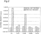
- Fig. 2 shows a change in electrical resistivity of the electrode layers 13 before and after the heat treatment.
- the horizontal axis represents the samples and the vertical axis represents the values of electrical resistivity of the samples before and after the heat treatment.
- Each of the samples that includes the barrier layer formed of Ti, Ni, Mo, or Ta is denoted by Cu/Ti, Cu/Ni, Cu/Mo, or Cu/Ta.
- Cu on the left end of the horizontal axis denotes the sample of the comparative example that was formed by producing the Cu electrode layer 13 directly on the ohmic contact layer 11.
- This electrical resistivity is larger than the electrical resistivity of the sample (Cu/Ni) that underwent the heat treatment. This clarifies that diffusion of Ni into the electrode layer 13 is more remarkable when the electrode layer is on nickel silicide than on Ni, and this fact has been demonstrated by actually analyzing the electrode layer 13.
- An increase in electrical resistivity of the electrode layer 13 increases a loss during energization to significantly deteriorate conversion efficiency of the SiC-MOSFET. Further, heat generation in the electrode layer 13 degrades device characteristics or decreases thermal conductivity correlated with the electrical resistivity to decrease thermal conduction in spite of using Cu high in thermally conductive properties for the electrode layer and further to possibly accelerate degradation of the device.
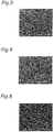
- Fig. 3 is a SEM photograph showing a surface of the sample (Cu/Mo) that includes the electrode layer 13 formed of Cu
- Fig. 4 is a SEM photograph showing a surface of the sample (Cu-1 at% Zn/Mo) that includes the electrode layer 13 formed of a Cu-Zn (Cu-1 at% Zn) alloy.
- Fig. 3 shows generation of voids along grain boundaries on the surface of the electrode layer 13.
- Fig. 4 shows no such void observed.
- Table 1 summarizes the electrical resistivity and the heat resistance of various samples that underwent a heat treatment.
- the ohmic contact layer 11 was formed of Ni, and the heat treatment conditions were set to 450°C for 1 hour.
- the evaluation of electrical resistivity was conducted according to the value of electrical resistivity of the electrode layer 13 that underwent the heat treatment, and a value of 4.0 ⁇ 10 -6 ⁇ cm or less was evaluated as acceptable ( ⁇ ) and a value of more than 4.0 ⁇ 10 -6 ⁇ cm was evaluated as unacceptable ( ⁇ ).
- the electrical resistivity never largely increases from before to after the heat treatment by using the barrier layer 12 formed of, for example, Mo.
- the electrical resistivity is large in the sample Cu-5 at% Zn due to a large ratio of Zn. In the meantime, no barrier layer component was observed in the electrode layers 13.
- Ni forms an all proportional solid solution with Cu, but forms no solid solution with Mo, and forms a compound with tungsten or niobium. That is, it is preferable to use, as the material for the barrier layer 12, a material that is non-solid soluble with Cu, that is, a material that forms no solid solution with Cu, or a material that forms a compound with Cu.
- grain boundary voids were observed on any of the electrode layers 13 formed of Cu, but addition of Zn to Cu in an amount of 0.1 to 5 at% suppressed generation of surface voids.
- the electrode layers 13 formed of Cu generate grain boundary voids by the heat treatment.
- the barrier layer 12 when the barrier layer 12 is not used, a constituent element diffused from the ohmic contact layer 11 into the Cu electrode has been confirmed to eventually improve the heat resistance of the Cu electrode layer.
- the diffusion of the constituent element from the ohmic contact layer 11 is considered to have been completely suppressed by the barrier layer 12 to generate grain boundary voids and thus make the heat resistance insufficient.
- Cu-1 at% Ni and Cu-1 at% Ti As a material having heat resistance to the heat treatment described above, there can be exemplified Cu-1 at% Ni and Cu-1 at% Ti, in addition to Cu-1 at% Zn in Table 1.
- the heat treatment generates a protrusion on a surface of the electrode layer formed of Cu-1 at% Ti but gives flatness on a surface of the electrode layer formed of Cu-1 at% Ni as in the case of the electrode layer formed of Cu-1 at% Zn.
- Table 2 shows comparative examples of an electrode that has a structure including no barrier layer 12, and Ni, Ti, Al, NiSi x (nickel silicide), and TiSi x (titanium silicide) were used as the materials for the ohmic contact layer 11.
- Used as the materials for the electrode layer 13 were Cu, a Cu-Ni alloy, and a Cu-Ti alloy.
- the heat treatment conditions are the same as in Table 1, i.e., 450°C for 1 hour.
- the evaluation of electrical resistivity was conducted in the same manner as in Table 1 according to the value of electrical resistivity of the electrode layer 13 that underwent the heat treatment, and a value of 4.0 ⁇ 10 -6 Qcm or less was evaluated as acceptable ( ⁇ ) and a value of more than 4.0 ⁇ 10 -6 Qcm was evaluated as unacceptable ( ⁇ ).
- the evaluation of heat resistance was conducted by observing with a SEM a surface of the electrode layer 13 that underwent the heat treatment, and the electrode layer that had no grain boundary void observed on the surface thereof was evaluated as ⁇ , the electrode layer that had a grain boundary void observed on the surface thereof was evaluated as ⁇ , the electrode layer that had a protrusion observed on the surface thereof was evaluated as ⁇ , and the electrode layer that had abnormal diffusion observed on the surface thereof was evaluated as ⁇ .
- the electrical resistivity after the heat treatment was larger than 4.0 ⁇ 10 -6 ⁇ cm in any comparative examples.
- the electrodes containing Cu as the material for the electrode layer 13 were improved in heat resistance. This is considered to be because the electrodes included no barrier layer 12 to allow the diffusion of the constituent element of the ohmic contact layer 11 into the electrode layer 13.
- the electrode that included the ohmic contact layer 11 formed of Ti had a protrusion observed on the surface of the electrode that underwent the heat treatment. This is because Ti diffused into Cu formed a compound with Cu, and the compound was generated as a protrusion on the surface.
- the electrodes that included the ohmic contact layer 11 formed of silicide were confirmed to have a large defect as shown in the SEM photograph of Fig. 5 showing a surface of an electrode layer. This is considered to be due to abnormal diffusion from silicide.
- the SiC-MOSFET is sometimes used in a use environment at higher temperature depending on the operation conditions.
- studied below are the results of samples that underwent a heat treatment at 450°C for 30 minutes or a heat treatment at 600°C for 5 minutes.
- an Al-based film (Al-1 at% Si film) was formed by sputtering on a thermal oxide film (silicon oxide film) that was produced on a surface of a silicon substrate and had a film thickness of 100 nm, and then subjected to the heat treatment at 450°C for 30 minutes or the heat treatment at 600°C for 5 minutes. A surface state of the Al-based film in either heat treatment was observed.
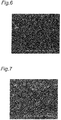
- Fig. 6 is a SEM photograph showing a surface of the Al-based electrode layer that underwent the heat treatment at 600°C for 5 minutes.
- the Al-based electrode layer had no abnormality observed on the surface thereof in the heat treatment at 450°C for 30 minutes, whereas the Al-based electrode layer generated a hillock as shown in Fig. 6 when undergoing the heat treatment at 600°C for 5 minutes.
- the electrode layer 13 formed of the Al-based material does not give heat resistance to 600°C or higher.
- the Al-based electrode layer generated a hillock on a surface thereof in the same manner.
- the conventional Al-based (Al-1 at% Si) electrode layer 13 generates mutual diffusion between the electrode layer and the material for the ohmic contact layer 11, such as Ni or NiSi.
- provision of the barrier layer 12 formed of Mo or TiN between the electrode layer 13 and the ohmic contact layer 11 is capable of reducing the mutual diffusion, but it is impossible to prevent diffusion of Ni with the barrier layer 12 formed of Ti.
- a Cu-based material is used for the electrode layer 13 to give, with appropriate selection of a barrier layer 12, an electrode layer 13 having good electrical resistivity even after a heat treatment, i.e., in a high temperature environment not only at 450°C but also at 600°C, thus enabling formation of an electrode layer 13 excellent in electrically conductive properties and thermally conductive properties.
- Fig. 7 is a SEM photograph of a surface of a sample (No. B-9 in Table 3) that contained Cu/Mo/NiSi for the electrode layer 13/barrier layer 12/ohmic contact layer 11 and underwent the heat treatment at 600°C for 5 minutes.
- Fig. 8 is a SEM photograph of a surface of a sample (No. B-11 in Table 3) that contained Cu-Zn/Mo/NiSi for the electrode layer 13/barrier layer 12/ohmic contact layer 11 and underwent the heat treatment at 600°C for 5 minutes.
- Fig. 7 clarifies generation of voids along grain boundaries in the Cu electrode layer 13.
- the generation of voids is more remarkable than in the case of the heat treatment at 450°C for 30 minutes.
- Fig. 8 clarifies reduction of generation of voids in the Cu-Zn electrode layer 13.
- Table 3 shows the evaluation results of electrical resistivity and heat resistance of various samples including the two samples described above that underwent the heat treatment at 450°C for 30 minutes or the heat treatment at 600°C for 5 minutes.
- all the samples included a SiO 2 film formed on a Si substrate and included a structure in Table 3 formed on the SiO 2 film.
- the ohmic contact layer 11 was formed of Ni or nickel silicide (NiSi), and the heat treatment conditions were set to 450°C for 30 minutes or 600°C for 5 minutes.
- the evaluation of electrical resistivity was conducted according to the value of electrical resistivity of the electrode layer 13 that underwent the heat treatment, and a value of 4.0 ⁇ 10 -6 ⁇ cm or less was evaluated as acceptable ( ⁇ ) and a value of more than 4.0 ⁇ 10 -6 ⁇ cm was evaluated as unacceptable ( ⁇ ).
- No. B-1 to B-7 in Table 3 show the results of evaluating the heat resistance of the single film of the Cu-based electrode layer 13, that is, the evaluation was conducted for the Cu-based electrode layer 13 produced on a thermal oxide film (silicon oxide film) that was produced on a surface of a silicon substrate and had a film thickness of 100 nm.
- the Cu-Ti electrode layer of No. B-4 had an electrical resistivity of larger than 4.0 ⁇ 10 -6 ⁇ cm after the heat treatment at 600°C for 5 minutes, and the Cu-Al electrode layer of No. B-5 formed a hillock on a surface thereof.
- No. B-2 (Cu-Ni), No. B-3 (Cu-Zn), No. B-6 (Cu-Ca), and No. B-7 (Cu-Mn) each had a low electrical resistivity even after the heat treatment at 600°C and were found to be excellent in heat resistance.
- No. B-8 to B-11 in Table 3 show the results of evaluating the Cu-based electrode layer 13 with Mo used for the barrier layer 12.
- Mutual diffusion was suppressed by the Mo barrier layer 12 even after the heat treatment at 600°C for 5 minutes, and the electrode layers exhibited excellent electrical resistivity and heat resistance.
- the samples did not show a reaction between Cu and Mo even after the heat treatment at 600°C for 5 minutes, and it is clarified that the Mo barrier layer 12 suppressed diffusion of an element from the NiSi ohmic contact layer 11. Further, it is also clarified that addition of an element such as Ni or Zn to the Cu electrode layer 13 is effective in order to improve the heat resistance of the Cu-based electrode layer 13 itself.
- No. B-12 to 20 in Table 3 show the results of evaluating the Cu-based electrode layer 13 with TiN used for the barrier layer 12. After the heat treatment at 450°C for 30 minutes, neither an increase in electrical resistivity nor an abnormal surface was observed. For example, as shown by No. B-14, mutual diffusion is found to be generated between the Cu electrode layer 13 and the TiN barrier layer 12 by the heat treatment at 600°C for 5 minutes. Particularly, use of the Ni-based ohmic contact layer 11 gives remarkable diffusion. The reason for this phenomenon is considered to be probably that TiN that is amorphous allows nitrogen to desorb from part of Ti and Ti to contribute to the diffusion. Ti forms an intermetallic compound with each of Cu and Ni, so that either Ti or Ni is assumed to be diffused into the Cu electrode.
- No. B-18 to 20 (Cu-Zn electrode layer 13/TiN barrier layer 12) had a smaller increase of the electrical resistivity than in the cases of the Cu electrode layers 13 of No. B-12 and 13.
- the Cu-Zn electrode layer 13 formed by pre-doping Cu with Zn is assumed to have suppressed diffusion of Ti from TiN.
- the electrode layer 13 formed of a Cu alloy such as Cu-Zn not only improves the heat resistance but also enables application of the TiN barrier layer 12 to the NiSi ohmic contact layer 11.
Landscapes
- Electrodes Of Semiconductors (AREA)
Abstract
Description
- The present invention relates to an ohmic electrode used in a SiC semiconductor device.
- SiC (silicon carbide) is a wide band gap semiconductor material and has high dielectric breakdown strength. Therefore, a SiC-containing MOSFET (MOS field-effect transistor) and the like are being developed as a next-generation power semiconductor device following a Si-IGBT (insulated gate bipolar transistor). An ohmic electrode (source/drain electrode) of the SiC-MOSFET includes an ohmic contact layer for forming an ohmic contact with a SiC substrate, and an electrode layer that is on the ohmic contact layer and has high electrically conductive properties. For the ohmic contact layer, for example, nickel silicide is used that is formed by subjecting Ni provided on the SiC substrate to a heat treatment at 800°C. For the electrode layer, an Al-based material such as Al or Al-Si is used that has high electrically conductive properties.
- The SiC-MOSFET has an ohmic electrode through which a larger current flows than in the Si-IGBT, so that the SiC-MOSFET has had a problem with the Al-based material in terms of heat resistance and durability. Particularly, the current concentrates on a connection part with a bonding wire, so that the connection part is probably locally heated up to 600°C or higher. Another problem has been that the SiC-MOSFET becomes relatively high temperature during its operation to cause a difference in coefficient of thermal expansion between the SiC substrate and the ohmic electrode and thus apply shear stress to the ohmic electrode, generating a crack and peeling with the Al-based material.
- Therefore, an object of the present invention is to provide an ohmic electrode that is used in a power semiconductor device including a SiC substrate, has good electrically conductive properties, is excellent in heat resistance and durability, and has high mechanical strength.
- The inventors have conducted earnest studies and have found as a result of the studies that a good ohmic electrode is obtained by using, as a material for the electrode layer, a Cu-Zn, Cu-Ni, Cu-Ti, Cu-Ca, or Cu-Mn alloy and forming a barrier layer to prevent diffusion of an ohmic contact material. Thus, the present invention has been completed.
- That is, the present invention is directed to an ohmic electrode that is used in a SiC semiconductor device, the ohmic electrode including an ohmic contact layer that is formed on a SiC semiconductor layer and is formed of a material selected from the group consisting of nickel and nickel silicide, a barrier layer formed on the ohmic contact layer, and an electrode layer that is formed on the barrier layer and is formed of a copper alloy containing at least one from among zinc, nickel, titanium, manganese, and calcium.
- The present invention is also a SiC semiconductor device including such an ohmic electrode.
- According to the present invention, it is possible to provide an ohmic electrode for a SiC semiconductor device that has good electrically conductive properties, is excellent in heat resistance and durability, and has high mechanical strength.
-
-
Fig. 1 is a sectional view of a SiC-MOSFET according to an embodiment of the present invention, -
Fig. 2 shows electrical resistivity of Cu electrode layers each formed on a barrier layer before and after a heat treatment, -
Fig. 3 is a SEM photograph showing a surface of a Cu electrode layer after a heat treatment, -
Fig. 4 is a SEM photograph showing a surface of a Cu alloy electrode layer after a heat treatment, -
Fig. 5 is a SEM photograph showing a surface of a Cu electrode layer formed on nickel silicide after a heat treatment, -
Fig. 6 is a SEM photograph showing a surface of an Al-based electrode layer after a heat treatment, -
Fig. 7 is a SEM photograph showing a surface of No. B-9 (Cu/Mo/NiSi) after a heat treatment at 600°C for 5 minutes, and -
Fig. 8 is a SEM photograph showing a surface of No. B-11 (Cu-Zn/Mo/NiSi) after a heat treatment at 600°C for 5 minutes. -
Fig. 1 is a sectional view of a SiC-MOSFET according to an embodiment of the present invention, generally represented by 100. The SiC-MOSFET 100 includes an n-type SiC substrate 1. An epitaxial layer (drift layer) 2 formed of n+SiC is provided on theSiC substrate 1. Aninsulating film 5 formed of, for example, silicon oxide, is provided on theepitaxial layer 2, and agate electrode 6 formed of, for example, polysilicon is provided on the insulating film. Here, thegate electrode 6 is covered around with theinsulating film 5. - A p-
type region 3 is provided in theepitaxial layer 2 and on both sides of thegate electrode 6, and an n-type region 4 is provided in the p-type region 3. The p-type region 3 and the n-type region 4 are formed by selectively introducing an impurity into theepitaxial layer 2 according to, for example, an ion implantation method or a thermal diffusion method. - An
ohmic contact layer 11 is provided on the n-type region 4. Theohmic contact layer 11 is formed of, for example, nickel silicide and has a film thickness of, for example, 100 nm. - The
ohmic contact layer 11 is formed by, for example, forming a Ni film on the n-type region 4 formed of SiC according to a sputtering method and then subjecting the Ni film to a heat treatment for a reaction of Si with Ni. - Below is one example of each of the sputtering conditions and the annealing conditions applied for producing the
ohmic contact layer 11. -
- Sputtering gas: argon
- Gas pressure: 2 mTorr
- Power: RF 400 W
-
- Temperature: 800°C
- Atmosphere: nitrogen
- In order to confirm formation of nickel silicide as a result of the reaction of Si in SiC with Ni under the annealing conditions described above, the following experiment was performed. First, a thermal oxide film (silicon oxide film) having a film thickness of 100 nm was formed on a Si substrate, and a sputtering layer having a film thickness of 100 nm was formed on the thermal oxide film by simultaneous discharge using a Ni target and a single-crystal Si target. The sputtering conditions are as follows.
-
- Sputtering gas: argon
- Gas pressure: 2 mTorr
- Power: RF 150 W (Ni target) and DC 400 W (Si target)
- Subsequently, the sputtering layer was subjected to a heat treatment under the annealing conditions (800°C, nitrogen atmosphere) described above and then to X-ray diffraction. This result clarified that the sputtering layer was formed into nickel silicide (Ni2Si, NiSi) and demonstrated that the
ohmic contact layer 11 was formed into nickel silicide under the annealing conditions described above. - In the SiC-
MOSFET 100, theohmic contact layer 11 is usually formed into nickel silicide by annealing at 800°C or higher. Part of the Ni layer, however, is not sometimes formed into silicide to leave Ni on a surface of theohmic contact layer 11 depending on the film thickness of the Ni layer, the heat treatment time, or the heat treatment temperature. - The
ohmic contact layer 11 is preferably formed of nickel silicide. Theohmic contact layer 11, however, may be formed of Ni, in addition to the case where part of the Ni layer is not formed into silicide and Ni remains as described above. - A
barrier layer 12 is provided on theohmic contact layer 11 to prevent mutual diffusion between the material for theohmic contact layer 11 and a material for anelectrode layer 13 formed on thebarrier layer 12. As a material for thebarrier layer 12, Mo is used, for example. Cu contained in theelectrode layer 13 forms an all proportional solid solution with Ni contained in theohmic contact layer 11 to easily generate mutual diffusion. Cu, however, forms no solid solution with Mo to hardly generate mutual diffusion. The mutual diffusion decreases conductivity of Cu and easily allows formation of a brittle mutual diffusion layer in an interface to degrade performance of the SiC-MOSFET 100. Used as the material for thebarrier layer 12 is, for example, Ta, W, Nb, Ti, or nitrides of these elements, in addition to Mo. Particularly, TiN that exhibits excellent electrically conductive properties is suitable for thebarrier layer 12. Thebarrier layer 12 has a film thickness of, for example, 50 nm. The film thickness may be selected within a range from 10 nm as a lower limit to 100 nm as an upper limit. - A sputtering method is used for producing the
barrier layer 12 and the film formation conditions when Mo is used as the material are as follows, for example. -
- Sputtering gas: argon
- Gas pressure: 2 to 10 mTorr
- Power: DC 260 to 500 W
- The film formation conditions when Ta, W, or Nb is used as the material are as follows, for example.
-
- Sputtering gas: argon
- Gas pressure: 2 mTorr
- Power: DC 260 to 500 W
- The film formation conditions when Ti is used as the material are as follows, for example.
-
- Sputtering gas: argon, nitrogen
- Gas pressure: 2 mTorr
- Power: DC 260 to 500 W
- Use of a nitride of Mo, Ta, W, Nb, or Ti as the material for the
barrier layer 12 has also been confirmed to be capable of preventing diffusion from theohmic contact layer 11 in the heat treatment. A nitride film is formed into amorphousness to give no grain boundary as a diffusion path of an element, so that an effect of suppressing the diffusion is considered to be enhanced. - When molybdenum nitride is used as the material for the
barrier layer 12, molybdenum nitride is produced using a molybdenum target and using a mixed gas of argon with nitrogen as a sputtering gas under the following sputtering conditions. -
- Sputtering gas: argon + nitrogen (flow rate of nitrogen gas to whole gas: 30%)
- Gas pressure: 2 mTorr
- Power: DC 500 W
- When titanium nitride is used as the material for the
barrier layer 12, titanium nitride is produced using a titanium target and using a mixed gas of argon with nitrogen as a sputtering gas under the following sputtering conditions. -
- Sputtering gas: argon + nitrogen (flow rate of nitrogen gas to whole gas: 50 to 90%)
- Gas pressure: 2 mTorr
- Power: DC 500 to 1000 W
- The
electrode layer 13 is formed on thebarrier layer 12. Theelectrode layer 13 is formed of, for example, an alloy of Cu and Zn (Cu-Zn), an alloy of Cu and Ni (Cu-Ni), an alloy of Cu and Ti (Cu-Ti), an alloy of Cu and Al (Cu-Al), an alloy of Cu and Ca (Cu-Ca), or an alloy of Cu and Mn (Cu-Mn). Theelectrode layer 13 has a film thickness of, for example, 300 to 4000 nm and is produced under the following conditions according to, for example, a sputtering method. -
- Sputtering gas: argon
- Gas pressure: 2 mTorr
- Power: DC 260 to 500 W
- The
ohmic contact layer 11, thebarrier layer 12, and theelectrode layer 13 that are formed as described above form asource electrode 10 of the SiC-MOSFET 100. - In the same manner as the
source electrode 10, anohmic contact layer 21, abarrier layer 22, and anelectrode layer 23 are sequentially produced also on a back surface of theSiC substrate 1 to form adrain electrode 20. Thus, the SiC-MOSFET 100 is completed. - As described above, in the SiC-
MOSFET 100 according to the embodiment of the present invention, the Cu alloy (Cu-Zn, Cu-Ni, Cu-Ti, Cu-Al, Cu-Ca, or Cu-Mn) that has good electrically conductive properties, thermally conductive properties, high heat resistance and mechanical strength has been used as the material for the electrode layers 13 and 23, in place of the Al-based material (such as Al or Al-Si) that has been conventionally used. - Further, in association with the use of the Cu alloy as the material for the electrode layers 13 and 23, the barrier layers 12 and 22 have been provided between the
ohmic contact layer 11 and theelectrode layer 13 and between theohmic contact layer 21 and theelectrode layer 23, respectively, to prevent mutual diffusion between the ohmic contact layers and the electrode layers, particularly diffusion of Ni from the ohmic contact layers 11 and 21 into the electrode layers 13 and 23. - This enables provision of an ohmic electrode for a SiC-MOSFET including an ohmic electrode that has good electrically conductive properties, is excellent in heat resistance and durability, and has high mechanical strength; and a SiC-MOSFET including such an ohmic electrode.
- Here, the SiC-MOSFET has been described. The ohmic electrode described above, however, can also be applied to another SiC-based semiconductor device such as a schottky barrier diode.
- Next, thermal stability is studied of
source electrodes 10 with the material for thebarrier layer 12 changed. Samples were each formed by producing anohmic contact layer 11 formed of nickel silicide on aSiC substrate 1, then producing abarrier layer 12 formed of Ti, Ni, Mo, or Ta on theohmic contact layer 11, and producing aCu electrode layer 13 on thebarrier layer 12. Thebarrier layer 12 and theelectrode layer 13 were made to have film thicknesses of 50 nm and 4000 nm, respectively. As a comparative example, a sample was also formed by stacking aCu electrode layer 13 directly on anohmic contact layer 11. - As the heat treatment conditions, the temperature was set to 450°C that is estimated as the temperature applied in a process of manufacturing a general semiconductor device. The heat treatment was performed in a nitrogen atmosphere for 1 hour. The electrode layers 13 were measured for electrical resistivity before and after the heat treatment and the effect of the barrier layers 12 was evaluated.
Fig. 2 shows a change in electrical resistivity of the electrode layers 13 before and after the heat treatment. - In
Fig. 2 , the horizontal axis represents the samples and the vertical axis represents the values of electrical resistivity of the samples before and after the heat treatment. Each of the samples that includes the barrier layer formed of Ti, Ni, Mo, or Ta is denoted by Cu/Ti, Cu/Ni, Cu/Mo, or Cu/Ta. Cu on the left end of the horizontal axis denotes the sample of the comparative example that was formed by producing theCu electrode layer 13 directly on theohmic contact layer 11. - As is clarified by
Fig. 2 , only the sample (Cu/Ni) that included the barrier layer formed of Ni remarkably increased the electrical resistivity, but the samples formed of the other materials (Cu/Ti, Cu/Mo, and Cu/Ta) were capable of preventing an increase in electrical resistivity caused by the heat treatment. - On the other hand, as shown by the comparative example, the sample (Cu) included no barrier layer formed severely increased the electrical resistivity of the
electrode layer 13 from 2.1 × 10⁻⁶ Ωcm to 1.35 × 10⁻⁵ Qcm. This electrical resistivity is larger than the electrical resistivity of the sample (Cu/Ni) that underwent the heat treatment. This clarifies that diffusion of Ni into theelectrode layer 13 is more remarkable when the electrode layer is on nickel silicide than on Ni, and this fact has been demonstrated by actually analyzing theelectrode layer 13. - An increase in electrical resistivity of the
electrode layer 13 increases a loss during energization to significantly deteriorate conversion efficiency of the SiC-MOSFET. Further, heat generation in theelectrode layer 13 degrades device characteristics or decreases thermal conductivity correlated with the electrical resistivity to decrease thermal conduction in spite of using Cu high in thermally conductive properties for the electrode layer and further to possibly accelerate degradation of the device. - With use of Mo, Ti, or Ta as the material for the barrier layer, however, it is possible to prevent the diffusion of Ni from the
ohmic contact layer 11 into theelectrode layer 13 to give anelectrode layer 13 having good electrical resistivity even after the heat treatment, thus enabling formation of anelectrode layer 13 excellent in electrically conductive properties and thermally conductive properties. - Next, as regards a sample (Cu/Mo) that included a
barrier layer 12 formed of Mo and samples that each included thesame barrier layer 12 and anelectrode layer 13 formed of a Cu-Zn alloy (Cu-0.1 at% Zn, Cu-1 at% Zn, Cu-2 at% Zn, or Cu-5 at% Zn), surface state of the electrode layers 13 that underwent a heat treatment were observed. The heat treatment conditions are the same as in the case ofFig. 2 , i.e., 450°C for 1 hour. -
Fig. 3 is a SEM photograph showing a surface of the sample (Cu/Mo) that includes theelectrode layer 13 formed of Cu, andFig. 4 is a SEM photograph showing a surface of the sample (Cu-1 at% Zn/Mo) that includes theelectrode layer 13 formed of a Cu-Zn (Cu-1 at% Zn) alloy.Fig. 3 shows generation of voids along grain boundaries on the surface of theelectrode layer 13.Fig. 4 , however, shows no such void observed. These facts clarify that because the generation of voids causes a decrease in heat resistance, addition of Zn to Cu as the material for theelectrode layer 13 suppresses the generation of voids during the heat treatment and improves the heat resistance. - Table 1 summarizes the electrical resistivity and the heat resistance of various samples that underwent a heat treatment. Here, the
ohmic contact layer 11 was formed of Ni, and the heat treatment conditions were set to 450°C for 1 hour. The evaluation of electrical resistivity was conducted according to the value of electrical resistivity of theelectrode layer 13 that underwent the heat treatment, and a value of 4.0 × 10⁻⁶ Ωcm or less was evaluated as acceptable (○) and a value of more than 4.0 × 10⁻⁶ Ωcm was evaluated as unacceptable (×). The evaluation of heat resistance was conducted by observing with a SEM theelectrode layer 13 that underwent the heat treatment, and the electrode layer that had no grain boundary void observed on a surface thereof was evaluated as acceptable (○) and the electrode layer that had a grain boundary void observed on a surface thereof was evaluated as unacceptable (×).[Table 1] Structure Electrical resistivity (Ωcm) Electrical resistivity Heat resistance Content rate of barrier layer component detected in electrode layer As-depo. After heat treatment Cu/Mo/Ni 2.00E-06 2.00E-06 ○ × 0at% Cu/Ta/Ni 2.00E-06 2.10E-06 ○ × 0at% Cu/W/Ni 2.00E-06 2.00E-06 ○ × 0at% Cu/Nb/Ni 2.00E-06 2.00E-06 ○ × 0at% Cu-0.1at%Zn/Mo/Ni 2.20E-06 2.10E-06 ○ ○ 0at% Cu-1at%Zn/Mo/Ni 3.30E-06 2.30E-06 ○ ○ 0at% Cu-2at%Zn/Mo/Ni 4.20E-06 2.70E-06 ○ ○ 0at% Cu-3at%Zn/Mo/Ni 5.50E-06 3.30E-06 ○ ○ 0at% Cu-5at%Zn/Mo/Ni 7.70E-06 4.90E-06 × ○ 0at% Cu-0.1at%Ni/Ni 2.20E-06 2.00E-06 ○ ○ 0at% Cu-1at%Ni/Mo/Ni 3.50E-06 2.70E-06 ○ ○ 0at% Cu-2at%Ni/Mo/Ni 4.60E-06 3.30E-06 ○ ○ 0at% Cu-3at%Ni/Mo/Ni 6.00E-06 4.20E-06 × ○ 0at% Cu-0.1at%Ti/Mo/Ni 2.50E-06 2.40E-06 ○ ○ 0at% Cu-0.5at%Ti/Mo/Ni 3.80E-06 3.50E-06 ○ ○ 0at% Cu-1at%Ti/Mo/Ni 4.50E-06 4.00E-06 × ○ 0at% - The electrical resistivity never largely increases from before to after the heat treatment by using the
barrier layer 12 formed of, for example, Mo. The electrical resistivity, however, is large in the sample Cu-5 at% Zn due to a large ratio of Zn. In the meantime, no barrier layer component was observed in the electrode layers 13. - Ni forms an all proportional solid solution with Cu, but forms no solid solution with Mo, and forms a compound with tungsten or niobium. That is, it is preferable to use, as the material for the
barrier layer 12, a material that is non-solid soluble with Cu, that is, a material that forms no solid solution with Cu, or a material that forms a compound with Cu. - As to the heat resistance, grain boundary voids were observed on any of the electrode layers 13 formed of Cu, but addition of Zn to Cu in an amount of 0.1 to 5 at% suppressed generation of surface voids.
- As shown in Table 1, the electrode layers 13 formed of Cu generate grain boundary voids by the heat treatment. On the other hand, when the
barrier layer 12 is not used, a constituent element diffused from theohmic contact layer 11 into the Cu electrode has been confirmed to eventually improve the heat resistance of the Cu electrode layer. In Table 1, however, the diffusion of the constituent element from theohmic contact layer 11 is considered to have been completely suppressed by thebarrier layer 12 to generate grain boundary voids and thus make the heat resistance insufficient. - As a material having heat resistance to the heat treatment described above, there can be exemplified Cu-1 at% Ni and Cu-1 at% Ti, in addition to Cu-1 at% Zn in Table 1. The heat treatment generates a protrusion on a surface of the electrode layer formed of Cu-1 at% Ti but gives flatness on a surface of the electrode layer formed of Cu-1 at% Ni as in the case of the electrode layer formed of Cu-1 at% Zn.
- In the meantime, it has also been confirmed that it is possible to suppress grain boundary voids by using, as the material for the
electrode layer 13, Cu-1 at% Ni described above, Cu-0.15 at% Ni-0.2 at% Nb, Cu-0.15 at% Ni-0.2 at% Al, or Cu-0.15 at% Ni-0.2 at% Mn, in addition to the samples indicated in Table 1. - Table 2 shows comparative examples of an electrode that has a structure including no
barrier layer 12, and Ni, Ti, Al, NiSix (nickel silicide), and TiSix (titanium silicide) were used as the materials for theohmic contact layer 11. Used as the materials for theelectrode layer 13 were Cu, a Cu-Ni alloy, and a Cu-Ti alloy. The heat treatment conditions are the same as in Table 1, i.e., 450°C for 1 hour. - The evaluation of electrical resistivity was conducted in the same manner as in Table 1 according to the value of electrical resistivity of the
electrode layer 13 that underwent the heat treatment, and a value of 4.0 × 10⁻⁶ Qcm or less was evaluated as acceptable (○) and a value of more than 4.0 × 10⁻⁶ Qcm was evaluated as unacceptable (×). The evaluation of heat resistance was conducted by observing with a SEM a surface of theelectrode layer 13 that underwent the heat treatment, and the electrode layer that had no grain boundary void observed on the surface thereof was evaluated as ○, the electrode layer that had a grain boundary void observed on the surface thereof was evaluated as ×, the electrode layer that had a protrusion observed on the surface thereof was evaluated as ▲, and the electrode layer that had abnormal diffusion observed on the surface thereof was evaluated as Δ.[Table 2] Structure Electrical resistivity before heat treatment Electrical resistivity after heat treatment Content rate of barrier layer component detected in electrode layer Heat resistance Cu/Ni ○ × 5.5at% ○ Cu/Ti ○ × 4.1at% ▲ Cu/Al ○ × 5.3at% ○ Cu-0.1at%Ni/Ni ○ × 4.9at% ○ Cu-1at%Ni/Ni ○ × 6.7at% ○ Cu-2at%Ni/Ni × × 8.8at% ○ Cu-0.1at%Ti/Ti ○ × 4.4at% ▲ Cu-1at%Ti/Ti × × 5.1at% ▲ Cu-2at%Ti/Ti × × 9.5at% ▲ Cu-0.1at%Al/Al ○ × 5.3at% ○ Cu-1at%Al/Al ○ × 4.9at% ○ Cu-2at%Al/Al × × 6.3at% ○ Cu/NiSix ○ × >10at% Δ Cu/TiSix ○ × >6at% Δ Cu-0.1at%Ni/NiSi ○ × >10at% Δ Cu-1at%Ni/NiSi ○ × >10at% Δ Cu-2at%Ni/NiSi × × >10at% Δ Cu-0.1at%Ti/TiSi ○ × >10at% Δ Cu-1at%Ti/TiSi × × >10at% Δ Cu-2at%Ti/TiSi × × >10at% Δ - The electrical resistivity after the heat treatment was larger than 4.0 × 10⁻⁶Ωcm in any comparative examples.
- On the other hand, as is clarified when Table 2 is compared with Table 1, the electrodes containing Cu as the material for the
electrode layer 13 were improved in heat resistance. This is considered to be because the electrodes included nobarrier layer 12 to allow the diffusion of the constituent element of theohmic contact layer 11 into theelectrode layer 13. The electrode that included theohmic contact layer 11 formed of Ti, however, had a protrusion observed on the surface of the electrode that underwent the heat treatment. This is because Ti diffused into Cu formed a compound with Cu, and the compound was generated as a protrusion on the surface. - The electrodes that included the
ohmic contact layer 11 formed of silicide (NiSi or TiSi) were confirmed to have a large defect as shown in the SEM photograph ofFig. 5 showing a surface of an electrode layer. This is considered to be due to abnormal diffusion from silicide. - The results in Table 2 clarify that the electrode that contains Cu or a Cu alloy as the material for the
electrode layer 13 is not practical without thebarrier layer 12 in consideration of both the electrical conductivity and the heat resistance after the heat treatment. - The SiC-MOSFET is sometimes used in a use environment at higher temperature depending on the operation conditions. Thus, studied below are the results of samples that underwent a heat treatment at 450°C for 30 minutes or a heat treatment at 600°C for 5 minutes.
- First, in order to evaluate the heat resistance of the
electrode layer 13 formed of a conventional Al-based material, an Al-based film (Al-1 at% Si film) was formed by sputtering on a thermal oxide film (silicon oxide film) that was produced on a surface of a silicon substrate and had a film thickness of 100 nm, and then subjected to the heat treatment at 450°C for 30 minutes or the heat treatment at 600°C for 5 minutes. A surface state of the Al-based film in either heat treatment was observed. -
Fig. 6 is a SEM photograph showing a surface of the Al-based electrode layer that underwent the heat treatment at 600°C for 5 minutes. The Al-based electrode layer had no abnormality observed on the surface thereof in the heat treatment at 450°C for 30 minutes, whereas the Al-based electrode layer generated a hillock as shown inFig. 6 when undergoing the heat treatment at 600°C for 5 minutes. Thus, theelectrode layer 13 formed of the Al-based material does not give heat resistance to 600°C or higher. - Further, even when a barrier film is provided between the Al-based electrode layer and the thermal oxide film, the Al-based electrode layer generated a hillock on a surface thereof in the same manner. The conventional Al-based (Al-1 at% Si)
electrode layer 13 generates mutual diffusion between the electrode layer and the material for theohmic contact layer 11, such as Ni or NiSi. Further, provision of thebarrier layer 12 formed of Mo or TiN between theelectrode layer 13 and theohmic contact layer 11 is capable of reducing the mutual diffusion, but it is impossible to prevent diffusion of Ni with thebarrier layer 12 formed of Ti. - In order to solve these problems, a Cu-based material is used for the
electrode layer 13 to give, with appropriate selection of abarrier layer 12, anelectrode layer 13 having good electrical resistivity even after a heat treatment, i.e., in a high temperature environment not only at 450°C but also at 600°C, thus enabling formation of anelectrode layer 13 excellent in electrically conductive properties and thermally conductive properties. -
Fig. 7 is a SEM photograph of a surface of a sample (No. B-9 in Table 3) that contained Cu/Mo/NiSi for theelectrode layer 13/barrier layer 12/ohmic contact layer 11 and underwent the heat treatment at 600°C for 5 minutes.Fig. 8 is a SEM photograph of a surface of a sample (No. B-11 in Table 3) that contained Cu-Zn/Mo/NiSi for theelectrode layer 13/barrier layer 12/ohmic contact layer 11 and underwent the heat treatment at 600°C for 5 minutes. -
Fig. 7 clarifies generation of voids along grain boundaries in theCu electrode layer 13. The generation of voids is more remarkable than in the case of the heat treatment at 450°C for 30 minutes. In contrast,Fig. 8 clarifies reduction of generation of voids in the Cu-Zn electrode layer 13. These facts clarify that because the generation of voids causes a decrease in heat resistance of theelectrode layer 13, addition of Zn to Cu as the material for theelectrode layer 13 suppresses the generation of voids during the heat treatment and improves the heat resistance. - Table 3 shows the evaluation results of electrical resistivity and heat resistance of various samples including the two samples described above that underwent the heat treatment at 450°C for 30 minutes or the heat treatment at 600°C for 5 minutes. Here, all the samples included a SiO2 film formed on a Si substrate and included a structure in Table 3 formed on the SiO2 film. The
ohmic contact layer 11 was formed of Ni or nickel silicide (NiSi), and the heat treatment conditions were set to 450°C for 30 minutes or 600°C for 5 minutes. - The evaluation of electrical resistivity was conducted according to the value of electrical resistivity of the
electrode layer 13 that underwent the heat treatment, and a value of 4.0 × 10⁻⁶ Ωcm or less was evaluated as acceptable (○) and a value of more than 4.0 × 10⁻⁶ Ωcm was evaluated as unacceptable (×). The evaluation of heat resistance was conducted by observing with a SEM theelectrode layer 13 that underwent the heat treatment, and the electrode layer that had no grain boundary void observed on a surface thereof was evaluated as acceptable (○), the electrode layer that had a grain boundary void observed on a surface thereof was evaluated as unacceptable (×), the electrode layer that had a protrusion observed on a surface thereof was evaluated as unacceptable (▲), and the electrode layer that had abnormal diffusion observed on a surface thereof was evaluated as unacceptable (Δ).[Table 3] No. Structure Electrical resistivity Ωcm Electrical resistivity Heat resistance As-depo. After heat treatment at 450°C After heat treatment at 600°C 450°C 600°C 450°C 600°C A-1 Al/Ni 4.2E-06 4.2E-06 1.5E-05 × × ▲ ▲ A-2 Al/NiSi 4.4E-06 1.0E-05 9.6E-06 × × ▲ ▲ A-3 Al/Ti/Ni 3.7E-06 1.8E-05 1.9E-05 × × Δ Δ A-4 Al/Ti/NiSi 3.7E-06 5.5E-06 1.0E-05 × × A A A-5 Al-1at%Si 4.7E-06 3. 4E-06 3.4E-06 ○ ○ ○ ▲ A-6 Al-1at%Si/Ni 4.4E-06 3.1E-06 1.7E-05 ○ × ○ Δ A-7 Al-1at%Si/NiSi 4.4E-06 1.1E-05 1.2E-05 × × Δ Δ A-8 Al-1at%Si/Mo 4.3E-06 3.6E-06 3.4E-05 ○ × ○ ▲ A-9 Al-1at%Si/Mo/Ni 4.0E-06 3.3E-06 4.4E-05 ○ × ○ ▲ A-10 Al-1at%Si/Mo/NiSi 4.0E-06 3.4E-06 4.1E-05 ○ × ○ ▲ A-11 Al-1at%Si/ Ti 4. 3E-06 4. 7E-06 2.9E-05 × × ○ ▲ A-12 Al-1at%Si/Ti/Ni 4.1E-06 4.9E-06 2.0E-05 × × Δ Δ A-13 Al-1at%Si/Ti/NiSi 4.0E-06 4.0E-06 1.4E-05 ○ × Δ Δ A-14 Al-1at%Si/TiN 4.3E-06 3.7E-06 4.9E-06 ○ × ○ ▲ A-15 Al-1at%Si/TiN/Ni 3.9E-06 3.2E-06 4.0E-06 ○ ○ ○ A A-16 Al-1at%Si/TiN/NiSi 4.1E-06 3.4E-06 4.6E-06 ○ × ○ ▲ B-1 Cu 2.3E-06 2.0E-06 2.0E-06 ○ ○ × × B-2 Cu-1at%Ni 3.8E-06 3.6E-06 3.4E-06 ○ ○ ○ ○ B-3 Cu-1at%Zn 2.2E-06 2.0E-06 2.0E-06 ○ ○ ○ ○ B-4 Cu-1at%Ti 1.1E-05 6.0E-06 4.2E-06 × × ▲ ▲ B-5 Cu- 1at%Al 4. 9E-06 3.1E-06 3.1E-06 ○ ○ ▲ ▲ B-6 Cu-1at%Ca 2.4E-06 2.3E-06 2.2E-06 ○ ○ ○ ○ B-7 Cu-1at%Mn 6.1E-06 2.9E-06 2.4E-06 ○ ○ ○ ○ B-8 Cu/Mo 2.4E-06 2.0E-06 2.0E-06 ○ ○ × × B-9 Cu/Mo/NiSi 2.3E-06 2.0E-06 2.3E-06 ○ ○ × × B-10 Cu-1at%Ni/Mo/NiSi 4.5E-06 3.4E-06 3.3E-06 ○ ○ ○ ○ B-11 Cu-1at%Zn/Mo/NiSi 2.9E-06 2.0E-06 2.0E-06 ○ ○ ○ ○ B-12 Cu/TiN 2.6E-06 2.0E-06 3.3E-06 ○ ○ × × B-13 Cu/TiN/Ni 2.2E-06 2.1E-06 1.2E-05 ○ × × Δ B-14 Cu/TiN/NiSi 2.1E-06 2.0E-06 5.1E-06 ○ × × × B-15 Cu-1at%Ni/TiN 4.0E-06 3.6E-06 5.1E-06 ○ × ○ ○ B-16 Cu-1at%Ni/TiN/Ni 4.0E-06 3.4E-06 1.4E-05 ○ × ○ Δ B-17 Cu-1at%Ni/TiN/NiSi 4.8E-06 3.6E-06 8.2E-06 ○ × ○ Δ B-18 Cu-1at%Zn/TiN 2.1E-06 2.0E-06 2.9E-06 ○ ○ ○ ○ B-19 Cu-1at%Zn/TiN/Ni 2.5E-06 1.9E-06 8.5E-06 ○ × ○ Δ B-20 Cu-1at%Zn/TiN/NiSi 2.8E-06 2.0E-06 3.3E-06 ○ ○ ○ ○ - No. B-1 to B-7 in Table 3 show the results of evaluating the heat resistance of the single film of the Cu-based
electrode layer 13, that is, the evaluation was conducted for the Cu-basedelectrode layer 13 produced on a thermal oxide film (silicon oxide film) that was produced on a surface of a silicon substrate and had a film thickness of 100 nm. The Cu-Ti electrode layer of No. B-4 had an electrical resistivity of larger than 4.0 × 10⁻⁶ Ωcm after the heat treatment at 600°C for 5 minutes, and the Cu-Al electrode layer of No. B-5 formed a hillock on a surface thereof. On the other hand, No. B-2 (Cu-Ni), No. B-3 (Cu-Zn), No. B-6 (Cu-Ca), and No. B-7 (Cu-Mn) each had a low electrical resistivity even after the heat treatment at 600°C and were found to be excellent in heat resistance. - No. B-8 to B-11 in Table 3 show the results of evaluating the Cu-based
electrode layer 13 with Mo used for thebarrier layer 12. Mutual diffusion was suppressed by theMo barrier layer 12 even after the heat treatment at 600°C for 5 minutes, and the electrode layers exhibited excellent electrical resistivity and heat resistance. The samples did not show a reaction between Cu and Mo even after the heat treatment at 600°C for 5 minutes, and it is clarified that theMo barrier layer 12 suppressed diffusion of an element from the NiSiohmic contact layer 11. Further, it is also clarified that addition of an element such as Ni or Zn to theCu electrode layer 13 is effective in order to improve the heat resistance of the Cu-basedelectrode layer 13 itself. - No. B-12 to 20 in Table 3 show the results of evaluating the Cu-based
electrode layer 13 with TiN used for thebarrier layer 12. After the heat treatment at 450°C for 30 minutes, neither an increase in electrical resistivity nor an abnormal surface was observed. For example, as shown by No. B-14, mutual diffusion is found to be generated between theCu electrode layer 13 and theTiN barrier layer 12 by the heat treatment at 600°C for 5 minutes. Particularly, use of the Ni-basedohmic contact layer 11 gives remarkable diffusion. The reason for this phenomenon is considered to be probably that TiN that is amorphous allows nitrogen to desorb from part of Ti and Ti to contribute to the diffusion. Ti forms an intermetallic compound with each of Cu and Ni, so that either Ti or Ni is assumed to be diffused into the Cu electrode. - On the other hand, No. B-18 to 20 (Cu-
Zn electrode layer 13/TiN barrier layer 12) had a smaller increase of the electrical resistivity than in the cases of the Cu electrode layers 13 of No. B-12 and 13. The Cu-Zn electrode layer 13 formed by pre-doping Cu with Zn is assumed to have suppressed diffusion of Ti from TiN. Theelectrode layer 13 formed of a Cu alloy such as Cu-Zn not only improves the heat resistance but also enables application of theTiN barrier layer 12 to the NiSiohmic contact layer 11. -
- 1
- SiC SUBSTRATE
- 2
- EPITAXIAL LAYER
- 3
- p-TYPE REGION
- 4
- n-TYPE REGION
- 5
- INSULATING FILM
- 6
- GATE ELECTRODE
- 10
- SOURCE ELECTRODE
- 20
- DRAIN ELECTRODE
- 11, 21
- OHMIC CONTACT LAYER
- 12, 22
- BARRIER LAYER
- 13, 23
- ELECTRODE LAYER
- 100
- SiC-MOSFET
Claims (6)
- An ohmic electrode comprising:an ohmic contact layer formed on a SiC semiconductor layer and formed of a material selected from the group consisting of nickel and nickel silicide;a barrier layer formed on the ohmic contact layer; andan electrode layer formed on the barrier layer and formed of a copper alloy containing at least one from among zinc, nickel, titanium, manganese, and calcium.
- The ohmic electrode according to claim 1, wherein the barrier layer is formed of an element that forms no solid solution with copper or an element that forms a compound with copper.
- The ohmic electrode according to claim 1, wherein the barrier layer is formed of a material selected from the group consisting of molybdenum, tantalum, tungsten, niobium, titanium, and nitrides of these elements.
- The ohmic electrode according to claim 1, wherein the electrode layer contains zinc and/or nickel in an amount of 0.1 at% or more and 3 at% or less, titanium in an amount of 0.1 at% or more and 0.5 at% or less, and/or manganese and/or calcium in an amount of 0.1 at% or more and 1 at% or less.
- The ohmic electrode according to claim 1, wherein the barrier layer has a film thickness of 10 nm or more and 100 nm or less.
- A SiC semiconductor device comprising the ohmic electrode according to any one of claims 1 to 5.
Applications Claiming Priority (3)
| Application Number | Priority Date | Filing Date | Title |
|---|---|---|---|
| JP2016032693 | 2016-02-24 | ||
| JP2016088311A JP6690985B2 (en) | 2016-02-24 | 2016-04-26 | Ohmic electrode |
| PCT/JP2017/003816 WO2017145694A1 (en) | 2016-02-24 | 2017-02-02 | Ohmic electrode |
Publications (2)
| Publication Number | Publication Date |
|---|---|
| EP3422389A1 true EP3422389A1 (en) | 2019-01-02 |
| EP3422389A4 EP3422389A4 (en) | 2019-10-23 |
Family
ID=59739131
Family Applications (1)
| Application Number | Title | Priority Date | Filing Date |
|---|---|---|---|
| EP17756136.2A Withdrawn EP3422389A4 (en) | 2016-02-24 | 2017-02-02 | OHMIC ELECTRODE |
Country Status (5)
| Country | Link |
|---|---|
| US (1) | US20190058048A1 (en) |
| EP (1) | EP3422389A4 (en) |
| JP (1) | JP6690985B2 (en) |
| KR (1) | KR20180116324A (en) |
| CN (1) | CN108701596A (en) |
Families Citing this family (5)
| Publication number | Priority date | Publication date | Assignee | Title |
|---|---|---|---|---|
| JP2019140234A (en) * | 2018-02-09 | 2019-08-22 | トヨタ自動車株式会社 | Semiconductor device |
| CN113424313B (en) * | 2019-02-18 | 2024-05-07 | 三菱电机株式会社 | Power semiconductor device and power conversion device |
| US10847647B2 (en) | 2019-03-14 | 2020-11-24 | Cree, Inc. | Power semiconductor devices having top-side metallization structures that include buried grain stop layers |
| WO2021028353A1 (en) * | 2019-08-09 | 2021-02-18 | Abb Schweiz Ag | Strain enhanced sic power semiconductor device and method of manufacturing |
| EP4071786B1 (en) * | 2021-04-06 | 2025-11-05 | Hitachi Energy Ltd | Method for forming an ohmic contact on a wide-bandgap semiconductor device and wide-bandgap semiconductor device |
Family Cites Families (10)
| Publication number | Priority date | Publication date | Assignee | Title |
|---|---|---|---|---|
| JP4091931B2 (en) * | 2004-07-13 | 2008-05-28 | 新電元工業株式会社 | SiC semiconductor device and method of manufacturing SiC semiconductor device |
| JP4038498B2 (en) * | 2004-07-13 | 2008-01-23 | 新電元工業株式会社 | Semiconductor device and method for manufacturing semiconductor device |
| JP4594113B2 (en) * | 2005-01-19 | 2010-12-08 | 新電元工業株式会社 | Manufacturing method of semiconductor device |
| JP2008166504A (en) * | 2006-12-28 | 2008-07-17 | Toshiba Corp | Field effect transistor and manufacturing method thereof |
| CN101842878B (en) * | 2007-10-24 | 2012-05-23 | 松下电器产业株式会社 | Semiconductor device and method for manufacturing the same |
| JP2011091364A (en) * | 2009-07-27 | 2011-05-06 | Kobe Steel Ltd | Wiring structure and method of manufacturing the same, as well as display apparatus with wiring structure |
| CN102227812A (en) * | 2009-10-05 | 2011-10-26 | 住友电气工业株式会社 | Semiconductor device |
| JP6324914B2 (en) * | 2010-11-25 | 2018-05-16 | 三菱電機株式会社 | Silicon carbide semiconductor device |
| JP5889171B2 (en) * | 2012-12-04 | 2016-03-22 | 三菱電機株式会社 | Silicon carbide semiconductor device and manufacturing method thereof |
| JP6010773B2 (en) * | 2014-03-10 | 2016-10-19 | パナソニックIpマネジメント株式会社 | Semiconductor device and manufacturing method thereof |
-
2016
- 2016-04-26 JP JP2016088311A patent/JP6690985B2/en not_active Expired - Fee Related
-
2017
- 2017-02-02 CN CN201780013111.8A patent/CN108701596A/en active Pending
- 2017-02-02 KR KR1020187026713A patent/KR20180116324A/en not_active Ceased
- 2017-02-02 EP EP17756136.2A patent/EP3422389A4/en not_active Withdrawn
- 2017-02-02 US US16/079,457 patent/US20190058048A1/en not_active Abandoned
Also Published As
| Publication number | Publication date |
|---|---|
| US20190058048A1 (en) | 2019-02-21 |
| JP2017152667A (en) | 2017-08-31 |
| CN108701596A (en) | 2018-10-23 |
| EP3422389A4 (en) | 2019-10-23 |
| KR20180116324A (en) | 2018-10-24 |
| JP6690985B2 (en) | 2020-04-28 |
Similar Documents
| Publication | Publication Date | Title |
|---|---|---|
| JP4995187B2 (en) | Power semiconductor device | |
| US20190058048A1 (en) | Ohmic electrode | |
| CN101536152B (en) | Ohmic electrode for SiC semiconductor, semiconductor device, and method for manufacturing the same | |
| US8264046B2 (en) | Synergy effect of alloying materials in interconnect structures | |
| US10651140B2 (en) | Semiconductor device with metal structure electrically connected to a conductive structure | |
| JP2014110362A (en) | Silicon carbide semiconductor device and manufacturing method of the same | |
| US7719030B2 (en) | Aluminum alloys for low resistance, ohmic contacts to III-nitride or compound semiconductor | |
| US9741805B2 (en) | Semiconductor device and method for manufacturing the semiconductor device | |
| KR20140036126A (en) | Method for segregating the alloying elements and reducing the residue resistivity of copper alloy layers | |
| US10224237B2 (en) | Semiconductor devices and methods for forming a semiconductor device | |
| DE102016104788B4 (en) | A semiconductor device having a metal adhesion and barrier structure and method of manufacturing a semiconductor device | |
| US9812328B2 (en) | Methods for forming low resistivity interconnects | |
| WO2017145694A1 (en) | Ohmic electrode | |
| CN105874566A (en) | Method for manufacturing silicon carbide semiconductor device | |
| US20260122993A1 (en) | Semiconductor device | |
| JPS6015970A (en) | Semiconductor device | |
| JP5846779B2 (en) | Semiconductor device and manufacturing method thereof | |
| JP2004289008A (en) | Semiconductor integrated circuit device and its manufacturing method | |
| KR20170037594A (en) | Semiconductor device comprising metal nitride electrode | |
| JP2025122761A (en) | Semiconductor Devices | |
| US6706630B1 (en) | Method for forming an alloyed metal conductive element of an integrated circuit | |
| KR101541656B1 (en) | Semiconductor element and method for manufacturing semiconductor element | |
| CN1981381A (en) | Schottky electrode of nitride semiconductor device and manufacturing method thereof | |
| Yang et al. | In-situ metal/dielectric capping process for electromigration enhancement in Cu interconnects | |
| JP2009124033A (en) | Semiconductor device and manufacturing method thereof |
Legal Events
| Date | Code | Title | Description |
|---|---|---|---|
| STAA | Information on the status of an ep patent application or granted ep patent |
Free format text: STATUS: THE INTERNATIONAL PUBLICATION HAS BEEN MADE |
|
| PUAI | Public reference made under article 153(3) epc to a published international application that has entered the european phase |
Free format text: ORIGINAL CODE: 0009012 |
|
| STAA | Information on the status of an ep patent application or granted ep patent |
Free format text: STATUS: REQUEST FOR EXAMINATION WAS MADE |
|
| 17P | Request for examination filed |
Effective date: 20180913 |
|
| AK | Designated contracting states |
Kind code of ref document: A1 Designated state(s): AL AT BE BG CH CY CZ DE DK EE ES FI FR GB GR HR HU IE IS IT LI LT LU LV MC MK MT NL NO PL PT RO RS SE SI SK SM TR |
|
| AX | Request for extension of the european patent |
Extension state: BA ME |
|
| DAV | Request for validation of the european patent (deleted) | ||
| DAX | Request for extension of the european patent (deleted) | ||
| A4 | Supplementary search report drawn up and despatched |
Effective date: 20190920 |
|
| RIC1 | Information provided on ipc code assigned before grant |
Ipc: H01L 29/45 20060101AFI20190916BHEP Ipc: H01L 21/28 20060101ALI20190916BHEP Ipc: H01L 29/78 20060101ALI20190916BHEP |
|
| STAA | Information on the status of an ep patent application or granted ep patent |
Free format text: STATUS: THE APPLICATION HAS BEEN WITHDRAWN |
|
| 18W | Application withdrawn |
Effective date: 20191028 |