EP3422055A1 - Scanner and scanner data generating method - Google Patents
Scanner and scanner data generating method Download PDFInfo
- Publication number
- EP3422055A1 EP3422055A1 EP18176495.2A EP18176495A EP3422055A1 EP 3422055 A1 EP3422055 A1 EP 3422055A1 EP 18176495 A EP18176495 A EP 18176495A EP 3422055 A1 EP3422055 A1 EP 3422055A1
- Authority
- EP
- European Patent Office
- Prior art keywords
- mirror
- concavity
- sensor
- walls
- light
- Prior art date
- Legal status (The legal status is an assumption and is not a legal conclusion. Google has not performed a legal analysis and makes no representation as to the accuracy of the status listed.)
- Withdrawn
Links
- 238000000034 method Methods 0.000 title claims description 29
- 230000003287 optical effect Effects 0.000 claims description 54
- 238000006243 chemical reaction Methods 0.000 description 51
- 230000008569 process Effects 0.000 description 18
- 230000000903 blocking effect Effects 0.000 description 14
- 239000000758 substrate Substances 0.000 description 14
- 230000002194 synthesizing effect Effects 0.000 description 7
- 230000015572 biosynthetic process Effects 0.000 description 5
- 230000006870 function Effects 0.000 description 5
- 238000003384 imaging method Methods 0.000 description 5
- 238000003786 synthesis reaction Methods 0.000 description 5
- 230000009467 reduction Effects 0.000 description 4
- 230000002452 interceptive effect Effects 0.000 description 3
- 238000005304 joining Methods 0.000 description 3
- 230000007246 mechanism Effects 0.000 description 3
- 239000003086 colorant Substances 0.000 description 2
- 238000001514 detection method Methods 0.000 description 2
- 238000010586 diagram Methods 0.000 description 2
- 238000005259 measurement Methods 0.000 description 2
- 238000012986 modification Methods 0.000 description 2
- 230000004048 modification Effects 0.000 description 2
- 230000032683 aging Effects 0.000 description 1
- 238000003491 array Methods 0.000 description 1
- 230000012447 hatching Effects 0.000 description 1
- 238000010191 image analysis Methods 0.000 description 1
- 238000004519 manufacturing process Methods 0.000 description 1
- 238000003860 storage Methods 0.000 description 1
Images









Classifications
-
- H—ELECTRICITY
- H04—ELECTRIC COMMUNICATION TECHNIQUE
- H04N—PICTORIAL COMMUNICATION, e.g. TELEVISION
- H04N1/00—Scanning, transmission or reproduction of documents or the like, e.g. facsimile transmission; Details thereof
- H04N1/00976—Arrangements for regulating environment, e.g. removing static electricity
- H04N1/00997—Light control, e.g. shielding from ambient light or preventing light leakage
-
- G—PHYSICS
- G02—OPTICS
- G02B—OPTICAL ELEMENTS, SYSTEMS OR APPARATUS
- G02B26/00—Optical devices or arrangements for the control of light using movable or deformable optical elements
- G02B26/08—Optical devices or arrangements for the control of light using movable or deformable optical elements for controlling the direction of light
- G02B26/10—Scanning systems
- G02B26/12—Scanning systems using multifaceted mirrors
- G02B26/125—Details of the optical system between the polygonal mirror and the image plane
- G02B26/126—Details of the optical system between the polygonal mirror and the image plane including curved mirrors
-
- G—PHYSICS
- G02—OPTICS
- G02B—OPTICAL ELEMENTS, SYSTEMS OR APPARATUS
- G02B5/00—Optical elements other than lenses
- G02B5/003—Light absorbing elements
-
- G—PHYSICS
- G02—OPTICS
- G02B—OPTICAL ELEMENTS, SYSTEMS OR APPARATUS
- G02B5/00—Optical elements other than lenses
- G02B5/12—Reflex reflectors
- G02B5/122—Reflex reflectors cube corner, trihedral or triple reflector type
- G02B5/124—Reflex reflectors cube corner, trihedral or triple reflector type plural reflecting elements forming part of a unitary plate or sheet
-
- H—ELECTRICITY
- H04—ELECTRIC COMMUNICATION TECHNIQUE
- H04N—PICTORIAL COMMUNICATION, e.g. TELEVISION
- H04N1/00—Scanning, transmission or reproduction of documents or the like, e.g. facsimile transmission; Details thereof
- H04N1/024—Details of scanning heads ; Means for illuminating the original
-
- H—ELECTRICITY
- H04—ELECTRIC COMMUNICATION TECHNIQUE
- H04N—PICTORIAL COMMUNICATION, e.g. TELEVISION
- H04N1/00—Scanning, transmission or reproduction of documents or the like, e.g. facsimile transmission; Details thereof
- H04N1/024—Details of scanning heads ; Means for illuminating the original
- H04N1/028—Details of scanning heads ; Means for illuminating the original for picture information pick-up
- H04N1/02815—Means for illuminating the original, not specific to a particular type of pick-up head
-
- H—ELECTRICITY
- H04—ELECTRIC COMMUNICATION TECHNIQUE
- H04N—PICTORIAL COMMUNICATION, e.g. TELEVISION
- H04N1/00—Scanning, transmission or reproduction of documents or the like, e.g. facsimile transmission; Details thereof
- H04N1/024—Details of scanning heads ; Means for illuminating the original
- H04N1/028—Details of scanning heads ; Means for illuminating the original for picture information pick-up
- H04N1/02815—Means for illuminating the original, not specific to a particular type of pick-up head
- H04N1/02895—Additional elements in the illumination means or cooperating with the illumination means, e.g. filters
-
- H—ELECTRICITY
- H04—ELECTRIC COMMUNICATION TECHNIQUE
- H04N—PICTORIAL COMMUNICATION, e.g. TELEVISION
- H04N1/00—Scanning, transmission or reproduction of documents or the like, e.g. facsimile transmission; Details thereof
- H04N1/024—Details of scanning heads ; Means for illuminating the original
- H04N1/028—Details of scanning heads ; Means for illuminating the original for picture information pick-up
- H04N1/03—Details of scanning heads ; Means for illuminating the original for picture information pick-up with photodetectors arranged in a substantially linear array
- H04N1/0301—Details of scanning heads ; Means for illuminating the original for picture information pick-up with photodetectors arranged in a substantially linear array using a bent optical path between the scanned line and the photodetector array, e.g. a folded optical path
- H04N1/0305—Details of scanning heads ; Means for illuminating the original for picture information pick-up with photodetectors arranged in a substantially linear array using a bent optical path between the scanned line and the photodetector array, e.g. a folded optical path with multiple folds of the optical path
-
- H—ELECTRICITY
- H04—ELECTRIC COMMUNICATION TECHNIQUE
- H04N—PICTORIAL COMMUNICATION, e.g. TELEVISION
- H04N1/00—Scanning, transmission or reproduction of documents or the like, e.g. facsimile transmission; Details thereof
- H04N1/024—Details of scanning heads ; Means for illuminating the original
- H04N1/028—Details of scanning heads ; Means for illuminating the original for picture information pick-up
- H04N1/03—Details of scanning heads ; Means for illuminating the original for picture information pick-up with photodetectors arranged in a substantially linear array
- H04N1/0306—Details of scanning heads ; Means for illuminating the original for picture information pick-up with photodetectors arranged in a substantially linear array using a plurality of optical elements arrayed in the main scan direction, e.g. an array of lenses
-
- H—ELECTRICITY
- H04—ELECTRIC COMMUNICATION TECHNIQUE
- H04N—PICTORIAL COMMUNICATION, e.g. TELEVISION
- H04N1/00—Scanning, transmission or reproduction of documents or the like, e.g. facsimile transmission; Details thereof
- H04N1/04—Scanning arrangements, i.e. arrangements for the displacement of active reading or reproducing elements relative to the original or reproducing medium, or vice versa
Definitions
- the present invention relates to a scanner and method of generating scanning data.
- a scanner configured to read image segments that partially overlap on a main scanning line by means of sensor chips corresponding to the individual segments, and generate scanning data for the main scanning line by synthesizing scanning data from plural segments respectively read by the plural sensor chips, is known from the literature. See, for example, JP-A-2013-131794 .
- concave mirrors corresponding one-to-one to each segment are disposed to the optical path through which light from segments partially overlapping each other in the main scanning line of a document, light (referred to below as stray light) other than the intended light from the segments the concave mirrors are designed to reflect may be incident to the concave mirrors. If stray light is reflected by a concave mirror and incident to the sensor, the image quality of the scanning data drops.
- An objective of the present invention is to improve the image quality of scanning data.
- a scanner has a first mirror having multiple concavities configured to reflect light from a document; a sensor configured to sense light reflected by a concavity of the first mirror; and a wall disposed to the first mirror and protruding from between the multiple concavities.
- the wall in this configuration can block unwanted light (stray light), that is, light other than light from the part of a document corresponding to each concavity, from reaching the sensor.
- stray light that is, light other than light from the part of a document corresponding to each concavity
- the sensor includes multiple sensor chips corresponding one-to-one with the concavities of the first mirror; and light from a defined range of a main scanning line of the document is reflected by a first concavity of the first mirror and input to a first sensor chip corresponding to the first concavity, and is reflected by a second concavity of the first mirror and input to a second sensor chip corresponding to the second concavity.
- This configuration can therefore generate scanning data for one main scanning line by synthesizing the scanning data in the range corresponding to the first sensor chip, and the scanning data in the range corresponding to the second sensor chip, based on the scanning data from the defined range.
- the first concavity and the second concavity are aligned adjacently in a main scanning direction; the sensor chips are aligned in the main scanning direction; and the wall protrudes from between the first concavity and the second concavity to a height Hdm equal to (0 ⁇ H dm ⁇ L- (q + W dm )/(2tan ⁇ 2 )) where: L is a distance to the first mirror from a virtual plane, which is a position where an image formed through the first mirror on the sensor chip is in focus; q is the length of the defined range on the main scanning line in the virtual plane; ⁇ 2 is the angle, in a plane including a principal ray from an end of the defined range and the main scanning line, between a perpendicular to the main scanning line and the principal ray; and W dm is a width in the main scanning direction of the wall disposed to a position equidistant from the first concav
- This aspect of the invention enables configuring a wall of a height that does not block at least the principal rays from the ends of the defined range.
- a scanner also has a second mirror having multiple concavities, and configured to reflect to the sensor, by corresponding concavities, light reflected by the multiple concavities of the first mirror; and an aperture that is different from the walls and is positioned between the first mirror and the second mirror on the optical path.
- this configuration Separately from an aperture provided between the first mirror and second mirror for the purpose of adjusting the amount of light incident to the sensor, this configuration provides walls located on the document side of the aperture in the optical path for the purpose of keeping stray light from striking the first mirror. Stray light on the document side of the aperture is therefore blocked by the walls.
- a scanner according to another aspect of the invention also has a second wall disposed to the second mirror and protruding from between multiple concavities of the second mirror.
- this configuration In addition to walls protruding from between the concavities of the first mirror, this configuration also has walls protruding from between the concavities of the second mirror. As a result, stray light can be blocked even more effectively.
- a scanner also has a third mirror having multiple concavities configured to reflect light from the document to a concavity corresponding to the first mirror; and an aperture that is different from the walls and is positioned between the third mirror and the first mirror on the optical path.
- this configuration Separately from an aperture provided between the third mirror and first mirror for the purpose of adjusting the amount of light incident to the sensor, this configuration provides walls located on the sensor side of the aperture in the optical path for the purpose of keeping stray light from striking the first mirror. Stray light on the sensor side of the aperture is therefore blocked by the walls.
- the walls are adjacent to concavities of the first mirror on both sides of the wall.
- Stray light is thereby blocked by the walls adjacent to concavities of the first mirror on both sides of the wall.
- the walls protrude from a ridge between concavities of the first mirror.
- the wall can prevent stray light being incident to the concavity from the gap.
- a protruding end of the wall is shaped conforming to the shape of the ridge formed by concavities of the first mirror.
- This configuration blocks stray light by a wall that is disposed between adjacent concavities and has a concave shape conforming to the shape (concave) of the ridge formed by adjacent concavities.
- another aspect of the invention is a scanning data generating method that is used by a scanner including a first mirror having multiple concavities configured to reflect light from a document, a sensor configured to sense light reflected by a concavity of the first mirror, and a wall disposed to the first mirror and protruding from between the multiple concavities; and includes steps of reading the document by the sensor and generating scanning data of the document.
- This method can block, by a wall, unwanted light (stray light), that is, light other than light from the part of a document corresponding to each concavity, from reaching the sensor.
- stray light that is, light other than light from the part of a document corresponding to each concavity
- Preferred embodiments of the present invention are described below in the following order: (1) scanner configuration, (2) shield wall configuration, (2-1) walls of a first mirror, (2-2) walls of an aperture member, (2-3) walls of a second mirror, (2-4) walls of a sensor substrate, (3) scanning process, (4) other embodiments.
- FIG. 1 is a block diagram of a scanner 1 according to this embodiment of the invention.
- the scanner 1 includes a controller 10, conveyance device 40, communicator 70, operating unit 80, computer 90, and a 2-channel reading unit (including light sources, sensors, and optical units).
- the controller 10 includes a recording medium not shown, and a processor that reads and executes a program from the recording medium.
- the processor may be a dedicated circuit device such as an ASIC embodied by circuits executing a specific process, or a CPU and ASIC that work together.
- the controller 10 controls parts of the scanner 1, and generates scanning data based on output from a reading unit.
- An operating unit 80 includes an output unit that provides information to the user, and an input unit for receiving input from the user.
- the controller 10 controls the operating unit 80 to display on the output unit information for selecting scanning conditions and instructing scanning, for example. Based on output from the output unit, the user can select scanning conditions and input start-scanning commands.
- the controller 10 controls parts of the scanner 1 to execute the operations for scanning a document (such as conveying the document).
- scanning data is output from the reading unit by this operation, the controller 10 generates scanning data.
- the communicator 70 is a device for communicating with an external device (an external computer 90 in this example), and the controller 10 can send desired information to the computer 90 and receive instructions and information from the computer 90 via the communicator 70.
- the controller 10 when the controller 10 produces scanning data, the controller 10 sends the scanning data through the communicator 70 to the computer 90.
- the scanning data may obviously be used in many ways, and may be stored on a recording medium not shown of the scanner 1, stored on a removable recording medium, or sent through the communicator 70 to a device other than the computer 90.
- the scanner 1 has both an automatic document feeder (ADF) not shown, and a scanning platen, and documents are scanned at the scanning position regardless of which is used.
- the scanner 1 according to this embodiment has a first reading unit and a second reading unit.
- the first reading unit can scan both moving documents (the front or first side) that are conveyed by the ADF, and stationary documents that are placed by the user directly on the scanning platen.
- the second reading unit can scan moving documents (the back or second side, the opposite side as the front), and cannot scan stationary documents.
- the first reading unit includes, as shown in FIG. 1 , a first sensor 21, a first light source 31, a sub-scanning device 41, and a first optical system 51.
- the sub-scanning device 41 is a device for moving the first sensor 21, first light source 31, and first optical system 51 bidirectionally in the sub-scanning direction.
- the second reading unit includes, as shown in FIG. 1 , a second sensor 22, a second light source 32, and a second optical system 52, and does not have a device equivalent to the sub-scanning device 41. More specifically, the second sensor 22, second light source 32, and second optical system 52 are stationary inside the scanner 1. Light from the second light source 32 is emitted to a specific position in the conveyance path of the moving document, and light from the moving document passes through the second optical system 52 and is sensed by the second sensor 22 to image the document.
- the first sensor 21 and second sensor 22 comprise multiple sensor chips.
- Each sensor chip forms a line sensor, which is a sensor extending in one direction, and comprises numerous photoelectric conversion elements arrayed in the one direction.
- each sensor chip has photoelectric conversion elements arranged in three rows, and a red (R), green (G), and blue (B) color filter is respectively disposed to the photoelectric conversion elements in each row.
- the direction in which the rows of photoelectric conversion elements extend is perpendicular to the sub-scanning direction (the conveyance direction of a moving document).
- the direction in which the photoelectric conversion elements are arrayed is referred to as the main scanning direction.
- the multiple sensor chips of the first sensor 21 are disposed at a specific interval in the main scanning direction.
- the multiple sensor chips of the second sensor 22 are disposed adjacently in the main scanning direction, and the interval between adjacent photoelectric conversion elements in different sensor chips is the same as the interval between photoelectric conversion elements in a sensor chip at a different position. In the second sensor 22, therefore, the multiple sensor chips are arrayed adjacently, and effectively form a line sensor for scanning one line in the main scanning direction.
- the first light source 31 and second light source 32 each have a lamp that emits light to a scanning area (exposure position) in the conveyance path of the moving document.
- a scanning area exposure position
- the exposure position moves in the sub-scanning direction.
- Light reflected from the object (a document or white calibration plate, for example) located at the exposure position is received by the sensor chips of the first sensor 21 or second sensor 22, and the sensor chips generate signals corresponding to the amount of light received by each photoelectric conversion element.
- the first sensor 21 and second sensor 22 have an analog front end, not shown.
- the analog front end includes a circuit that applies gain to the signals output by the photoelectric conversion elements according to the amount of light received, and an analog/digital conversion (ADC) circuit.
- ADC analog/digital conversion
- the analog front end in this example also has a recording medium for recording information indicating the gain, and the analog front end, based on the gain information, adjusts the gain of the black level of the first sensor 21 and second sensor 22 to the lowest output value, and the white level to the highest output level.
- the first light source 31 and second light source 32 are light sources that output white light. Because the photoelectric conversion element arrays of the first sensor 21 and second sensor 22 are equipped with RGB color filters, the first sensor 21 and second sensor 22 can generate RGB scanning data based on the light from a document exposed to white light.
- the conveyance device 40 is a mechanism that conveys documents.
- the conveyance device 40 conveys the moving document to the position exposed to light from the first light source 31, and the position exposed to light from the second light source 32, and then conveys the moving document out from the scanner 1.
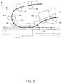
- FIG. 2 schematically illustrates the conveyance path of the conveyance device 40.
- the conveyance path comprises plastic members not shown forming the path of the moving document, and a moving document is conveyed through the conveyance path by opposing conveyance rollers 40a, 40b disposed at multiple positions along the path.
- the conveyance path is indicated by the curve of the heavy solid line in FIG. 2 .
- the exposure positions on the conveyance path are indicated by the dotted lines, and one line in the main scanning direction (direction perpendicular to the X-axis and Z-axis) is read at the exposure position by the first sensor 21 and second sensor 22.
- Light from the area of one line on a document is therefore split into light from multiple areas of which the ends in the main scanning direction overlap, and each of the split light beams is focused on a sensor chip.
- the output from the sensor chips of the first sensor 21 must be synthesized to generate one line of scanning data.
- a merging mark used as an index for synthesizing data is therefore formed on the calibration plate 61 in this embodiment of the invention.
- the merging mark is formed at a position where areas overlap at the ends of adjacent areas, and by scanning the merging mark when a document is not on the platen, the photoelectric conversion elements that read the same position can be identified in the output of the sensor chips.
- the calibration plate 61 includes a white calibration plate and a black calibration plate for gain adjustment, the white level is determined based on the result measured with the white calibration plate, and the black level is determined based on the result measured with the black calibration plate.
- the calibration plate 61 may be configured with a moving part, and disposed so that the target selected from among the merging mark, white calibration plate, and black calibration plate is moved by the moving part and set to the exposure position.
- calibration plate 62 also has a white calibration plate and a black calibration plate.
- the sub-scanning device 41 is a device capable of moving the first unit U1 bidirectionally in the sub-scanning direction (X-axis).
- the sub-scanning device 41 sets the first unit U1 to a defined position as shown in FIG. 2 .
- the document is then scanned with the first unit U1 at this specific position.
- the sub-scanning device 41 moves the first sensor 21, first light source 31, and first optical system 51 in the sub-scanning direction to scan the document.
- the area indicated in FIG. 2 by the dotted line and the dot-dash line connected to the dotted line is the exposure position (the document scanning range), and the exposure position can move in the sub-scanning direction.
- the second sensor 22, second light source 32, and second optical system 52 of the second reading unit are disposed in the second unit U2 shown in FIG. 2 .
- the second reading unit is a CIS (contact image sensor).
- the first optical system 51 includes an optical member (reduction optics system) for reducing and converging an image of the document on the first sensor 21. More specifically, the first optical system 51 has a member forming an optical path guiding, to the sensor chip, light from the document produced by the first light source 31 emitting light to the document.
- the optical path may be configured in many ways, and can be configured from combinations of various members, including an aperture member, lenses, and mirrors.
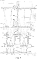
- FIG. 3 illustrates the first optical system 51 in this embodiment of the invention as viewed parallel to the main scanning direction.
- the configuration in FIG. 3 shows the first light source 31 that emits light to the document P, first optical system 51 (51a to 51h), and a first sensor 21.
- a first optical system 51 uses configurations which include a first mirror 51a with multiple concavities, a second mirror 51b with multiple concavities, an aperture member 51c having multiple openings that function as apertures; and walls (51d to 51h) for blocking stray light; and guides the light to the sensor chip 21a by splitting the light from one line in the main scanning direction of the document P (the direction perpendicular to the X-axis and Z-axis) into multiple areas that overlap in part in the main scanning direction, and reducing the image of each area.
- the light beam reflected from a desired area on the main scanning line is indicated by the three lines. More specifically, the principal ray, which is the light ray in the center of the light beam, is indicated by a dot-dash line, and the rays on the outside of the light beam are indicated by the dot-dot-dash lines.
- FIG. 4 schematically illustrates the operation of the optical system with the main scanning direction on the horizontal axis.
- the concavity 51ai of the first mirror 51a, and the concavity 51bi of the second mirror 51b are represented by ovals representing replacement by equivalent lenses with the outgoing beam leaving the lens from the opposite side from which the incident beam enters.
- the concavities 51ai of the first mirrors 51a and the concavities 51bi of the second mirrors 51b also correspond one-to-one.
- the sensor chips 21a of the first sensor 21 are provided on a substrate 210.
- the sensor chip 21a extends in the main scanning direction (Y-axis), and images of adjacent parts of the document P that partially overlap in the main scanning direction are reduced in the parts of the first optical system 51 corresponding to those parts of the document P.
- the images from each area of the document P are then focused on the sensor chip 21a corresponding to those parts. More specifically, an image of the area of length LP in the main scanning direction is focused on a sensor chip 21a of length d.
- One-to-one imaging optics that form images on the second sensor 22 without reducing the size are used in the second optical system 52.
- the controller 10 therefore does not need to apply the synthesizing process to the output of the second sensor 22, and applies another imaging process (such as cropping or edge enhancement) to acquire the scanning data.
- the controller 10 must synthesize data output from adjacent sensor chips where the outputs coincide to generate the scanning data. More specifically, the controller 10, based on the read results of the merging mark formed on the calibration plate 61, superimposes the outputs of the sensor chips 21a. More specifically, as shown in FIG. 4 , the first sensor 21 is embodied by multiple sensor chips 21a, and the multiple sensor chips 21a are disposed at different positions.
- each sensor chip 21a When the same positions are read by different sensor chips 21a, the same positions are read at the ends of the sensor chips 21a. Because these same positions are where the merging marks are disposed on the calibration plate 61, when the merging mark is read without a document present, each sensor chip 21a outputs data capturing the merging mark.
- FIG. 5 schematically illustrates the photoelectric conversion elements of the sensor chip 21a, the black dots denoting the photoelectric conversion elements.
- the merging mark is a line extending in the sub-scanning direction, and the areas around the merging mark are white.
- the merging mark is read by each pair of adjacent sensor chips 21a.
- the photoelectric conversion elements of the sensor chips 21a that read the merging mark are indicated by black dots
- the merging mark is indicated by hatching
- the photoelectric conversion elements that read the merging mark are shown overlapping.
- One of the adjacent sensor chips 21a is located on the top left side, the other is located on the bottom right side, and the sensor chips 21a are shown schematically so that the photoelectric conversion elements that read the merging mark are vertically aligned.
- One of the two adjacent sensor chips 21a is referred to below as first sensor chip 21a1, and the other as second sensor chip 21a2.
- the first sensor chip 21a1 and second sensor chip 21a2 output, as serial data, signals corresponding to the amount of light detected by the photoelectric conversion elements aligned in the main scanning direction.
- the controller 10 analyzes the output of the first sensor chip 21a1, and determines that the merging mark was detected by the fifth and sixth photoelectric conversion elements E5, E6 from the end.
- the controller 10 also analyzes the output of the second sensor chip 21a2, and determines that the merging mark was detected by the fourth and fifth photoelectric conversion elements E4, E5 from the end.
- the controller 10 determines that the fifth and sixth photoelectric conversion elements E5, E6 of the first sensor chip 21a1, and the fourth and fifth photoelectric conversion elements E4, E5 of the second sensor chip 21a2, read the same position, and in memory not shown stores the locations of the corresponding elements in each sensor chip 21a.
- the controller 10 applies the above process sequentially from the end of the sensor chips 21a in the main scanning direction, and identifies the location of the photoelectric conversion elements that read the same position in each sensor chip 21a.
- any of the sensor chips other than the sensor chips at the ends may be either a first sensor chip 21a1 or a second sensor chip 21a2.
- one sensor chip 21a is the first sensor chip 21a1 and then becomes the adjacent second sensor chip 21a2 such that the second sensor chip 21a2 is treated as the first sensor chip 21a1, the sensor chip 21a adjacent thereto on the opposite side becomes the second sensor chip 21a2.
- the controller 10 generates one line of scanning data by synthesizing the outputs of the sensor chips 21a based on their respective positions.
- the first optical system 51 has walls (51d to 51h) for preventing stray light, which is light other than the light on the optical paths shown in FIG. 3 and FIG. 4 , from being incident to the sensor chips 21a.
- Walls 51d shown in FIG. 3 are shield walls disposed on the first mirror 51a.
- walls 51d include walls 51dm, and walls 51ds connecting one wall 51dm with the adjacent wall 51dm.
- the walls 51dm are disposed adjacent to two adjacent concavities.
- the walls 51dm protrude from the ridge line R between two adjacent concavities, and there is no gap between the ridge line R and the walls 51dm (the bottom of the wall 51dm is in contact with the ridge line R).
- the walls 51ds from a grid pattern (or a ladder shape) when seen from the Z-axis, and one concavity can be seen from one opening between walls 51ds.
- the protruding distal ends To of the walls 51dm have a concave shape conforming to the shape of the ridge line R.
- the walls 51ds and walls 51dm surround the edges of the concavity 51ai.
- the shape (wall thickness and height) of the walls 51dm is described below with reference to FIG. 7 .
- FIG. 7 schematically illustrates the configuration of the walls on the optical path through which light reflected from the document P is guided to a sensor chip 21a.
- the target concavity is referred to as the first concavity 51a1
- the concavity adjacent to the first concavity 51a1 is referred to as the second concavity 51a2.
- the concavity of the first mirror 51a and the concavity of the second mirror 51b are represented by convex lenses.
- the light beam (conical shapes) representing light reflected from a desired position on the main scanning line (scan line) of the document P are indicated by the three lines (the principal ray, which is the light ray in the center of the light beam, indicated by a dot-dash line, and the rays on the outside of the light beam indicated by the dot-dot-dash lines).
- the thickness (width W dm ) of the walls 51dm in this example is constant, and the wall 51dm between a first concavity 51a1 and a second concavity 51a2 is disposed at a position equidistant from the first concavity 51a1 and second concavity 51a2.
- the overlapping portions (referred to below as the defined range) of the range P1 and second range P2 are read by both the first sensor chip 21a1 and the second sensor chip 21a2.
- the length of the defined range in the main scanning direction is length q.
- the wall height must be limited to a height at which at least the principal ray from the end P 1R on the second concavity 51a2 side of the defined range where range P1 and second range P2 overlap is not blocked. Therefore, the wall 51dm disposed between the first concavity 51a1 and second concavity 51a2 of the first mirror 51a protrudes from point p02 on the ridge line R to height Hdm defined by equation (1). 0 ⁇ Hdm ⁇ L ⁇ q + W dm / 2 tan ⁇ 2
- L is the distance from a virtual plane, which is the position where the image formed through the first mirror 51a on the sensor chip 21a is in focus, to the first mirror 51a.
- the relative positions of the scanning platen T (not shown in FIG. 7 ) and first optical system 51 are designed so that the document P is positioned on this virtual plane. The following description supposes that the read side of the document P is position on this virtual plane. More specifically, length L is the distance from point p02 to the document P end P 1R on a plane parallel to the XZ plane.
- the first mirror 51a is disposed extending in the main scanning direction (Y-axis), and the walls 51dm protrude from the ridge line R of the first mirror 51a in the direction parallel to the XZ plane.
- Point p02 is described below with reference to FIG. 8 and FIG. 9 .
- FIG. 8 is an oblique view of the first mirror 51a omitting for clarity the wall 51ds shown on the -X-axis side in the oblique view in FIG. 6 .
- FIG. 9 schematically illustrates the wall 51dm between the first concavity 51a1 and the second concavity 51a2 as seen from the -Y-axis side to the +Y-axis side.
- Point p01 is the point where the principal ray Rc of the light reflected from the second concavity 51a2 side end P 1R (see FIG. 7 ) of the defined range, which is where range P1 and second range P2 overlap, is incident to the first concavity 51a1.
- the principal ray Rc from end P 1R projected to the side (a plane parallel to the XZ plane) of the wall 51dm on the first concavity 51a1 side is ray Rcc as shown in FIG. 9 .
- Point p02 is at the intersection of ray Rcc and the ridge line (see FIG. 8 and FIG. 9 ) on the first concavity side of the ridge line R formed by the first concavity 51a1 and second concavity 51a2.
- ⁇ 2 in equation (1) is the angle, in a plane including the main scanning line of the document P and the principal ray Rc incident to the first concavity 51a1 from end P 1R , between the perpendicular to the main scanning line and the principal ray Rc.
- W dm is the width in the main scanning direction (Y-axis) of the wall 51dm located equidistantly from the first concavity 51a1 and second concavity 51a2.
- Point p05 is the intersection between ray Rcc and principal ray Rc. Note that the Y coordinate of the center of the length q of the defined range on the Y-axis, and the Y coordinate of the center of the wall 51dm on the Y-axis, are the same, and wall 51dm is parallel to the XZ plane. Therefore, (q + W dm )/(2tan ⁇ 2 ) in equation (1) means the length of line k1. As shown in FIG.
- the wall 51dm is formed so that the length (height Hdm) from point p02 parallel to the ray Rcc is less than (L - k1).
- the wall 51dm can be configured to not obstruct at least the principal ray Rc incident to the first concavity 51a1 from the end P 1R of the defined range.
- data can be synthesized using the merging mark even if ray Re on the outside side of the light beam from the principal ray Rc and closest to the second concavity 51a2 side are blocked by the wall 51dm. More specifically, data can be synthesized using a merging mark in scanning data with a reduced amount of light around the merging mark.
- the light beam of the reflected light from the end P 1R detected by the second sensor chip 21a2 includes rays on the outside side of the principal ray, the image quality of scanning data after synthesis of the position at the end P 1R is not affected.
- the height Hdm of the wall 51dm from point p02 can be set to a height not obstructing ray Re if height Hdm satisfies equation (2) below. 0 ⁇ Hdm ⁇ L ⁇ q + W dm / 2 tan ⁇ 1
- ⁇ 1 is the angle, in a plane (the same plane as the plane including the main scanning line and principal ray Rc) including the main scanning line of the document P and the ray Re closest to the second concavity 51a2 side of the light beam incident to the first concavity 51a1 from end P 1R , between the perpendicular to the main scanning line and the principal ray Re.
- Point p04 is the intersection of ray Rcc (ray Re from end P 1R projected to the side (a plane parallel to the XZ plane) of the wall 51dm on the first concavity 51a1 side) and ray Re.
- (q + W dm )/(2tan ⁇ 2 ) means the length of line k2.
- wall 51dm is formed so that the height Hdm from point p02 satisfies equation (2). More specifically, the figures show a wall 51dm of Hdm ⁇ L - k2.
- the other walls 51dm of the first mirror 51a are formed in the same way as the wall 51dm between the first concavity 51a1 and second concavity 51a2.
- the walls 51ds joining the walls 51dm are disposed in contact with the sub-scanning direction (X-axis) edges of the concavities between one wall 51dm and the next wall 51dm. There is no gap between the X-axis end of a concavity and the wall 51ds.
- the wall 51ds may be formed to any height not blocking the beam of the light incident to the concavities and the beam of light reflected from the concavities; and the height of walls 51ds on the side of light incident to the concavities and the height of walls 51ds on the side of light outgoing from the concavities may be the same or different.
- the walls 51ds on the side of the incident light are higher than the walls 51ds on the side of outgoing light.
- An aperture member 51c is a flat member extending in the main scanning direction (Y-axis), and a plurality of apertures (openings) are formed in the main scanning direction. As shown in FIG. 7 , the aperture corresponding to the first concavity 51a1 is referred to as the first aperture 51c1, and the aperture corresponding to the second concavity 51a2 is referred to as the second aperture 51c2.
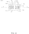
- FIG. 10 shows the aperture member 51c from the document P side of the optical path.
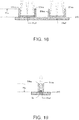
- FIG. 11 is a section view through f11- f11 in FIG. 10
- FIG. 12 is a section view through f12 - f12 in FIG. 10 .
- Walls 51e are shield walls protruding from the aperture member 51c to the document P side of the optical path, and as shown in FIG. 10 , include walls 51em disposed between the multiple apertures formed in the aperture member 51c, and walls 51es joining one wall 51em to another wall 51em. By connecting walls 51es by a pair of walls 51em, the strength of the walls 51em is increased and the angle of the walls 51em to the surface of the aperture member 51c is stable.
- walls 51e are shield walls protruding from the aperture member 51c to the sensor chip side of the optical path, and like the walls 51e shown in FIG. 10 , include walls 51fm disposed between the multiple apertures, and walls 51fs joining one wall 51fm to another wall 51fm. By connecting walls 51fs by a pair of walls 51fm, the strength of the walls 51fm is increased and the angle of the walls 51fm to the surface of the aperture member 51c is stable.
- the walls 51em disposed on opposite sides of the first aperture 51c1 protrude from the aperture member 51c to a height and position not blocking the principal rays Rc (in this example, the two principal rays incident to the photoelectric conversion elements at both ends in the main scanning direction of the first sensor chip 21a1 corresponding to the first aperture 51c1).
- the walls 51em may also be disposed to a height Hem and position not blocking the outside-most rays Re, in addition to the principal rays Rc in the light beam incident to the photoelectric conversion elements at both ends in the main scanning direction of the first sensor chip 21a1.
- the other walls 51em disposed to the aperture member 51c are also disposed with the same shape described above.
- the walls 51es connecting one wall 51em to another wall 51em are disposed to a height Hes not obstructing light beams incident to the corresponding sensor chip (first sensor chip 21a1 in this example).
- the other walls 51es disposed to the aperture member 51c are also disposed with the same shape described above.
- the walls 51fm disposed on opposite sides of the first aperture 51c1 protrude from the aperture member 51c to a height and position not blocking the principal rays Rc incident to the ends of the first sensor chip 21a1 in the main scanning direction.
- the walls 51fm may also be disposed to a height Hfm and position not blocking the rays Re closest to the second aperture 51c2, in addition to the principal rays Rc in the light beam incident to the first sensor chip 21a1.
- the other walls 51fm disposed to the aperture member 51c are also disposed with the same shape described above.
- the walls 51fs connecting one wall 51fm to another wall 51fm are disposed to a height Hfs not obstructing light beams incident to the corresponding sensor chip (first sensor chip 21a1 in this example).
- the other walls 51fs disposed to the aperture member 51c are also disposed with the same shape described above.
- the second mirror 51b has multiple concavities, and reflects light reflected from the multiple concavities of the first mirror 51a by the corresponding concavities to the corresponding sensor chip 21a.
- FIG. 13 illustrates the surface on which the concavities of the second mirror 51b are formed. Shown in FIG. 13 are the first concavity 51b1 corresponding to the first aperture 51c1, and the second concavity 51b2 corresponding to the second aperture 51c2.
- FIG. 14 is a section view through line f14-f14 in FIG. 13
- FIG. 15 is a section view through line f15-f15 in FIG. 13
- FIG. 16 is a section view through line f16-f16 in FIG. 13 .
- walls 51g include walls 51gm (examples of second walls) disposed between adjacent concavities of the second mirror 51b, and walls 51gs connecting adjacent walls 51gm.
- a wall 51gm disposed between a first concavity 51b1 and a second concavity 51b2 is disposed adjacent to the concavity on each side.
- the walls 51gm protrude from the ridge line R formed by the first concavity 51b1 and second concavity 51b2, and there is no gap between the ridge line R and the wall 51gm.
- the protruding distal end To of the wall 51gm is concave, following the shape of the ridge line R as shown in FIG. 16 .
- the walls 51gs enclose the edges of the walls 51gm, first concavity 51b1, and second concavity 51b2. By the walls 51gs connecting the walls 51gm, the strength of the walls 51gm is improved, and the angle of the walls 51gm to the optical path is stable.
- the thin dot-dash lines indicate the principal ray in the beam of incident light passing through the corresponding aperture and incident to a concavity of the second mirror 51b, and the thin dot-dot-dash lines indicate rays on the outside side of the light beam.
- the bold dot-dash lines indicate the principal ray in the beam of reflected light from a concavity of the second mirror 51b to the corresponding sensor chip 21a, and the bold dot-dot-dash lines indicate rays on the outside side of the light beam.
- the walls 51gm disposed on both sides of the first concavity 51b1 are configured in a shape protruding from the ridge line R in a shape (height Hgm, width Wgm) not interfering with the principal rays of the light beams incident to the photoelectric conversion elements located at the opposite ends in the main scanning direction (Y-axis) of the first sensor chips 21a1 corresponding to the first concavity 51b1.
- the thin dot-dash lines indicate the principal ray in the beam of incident light passing through the first aperture 51c1 corresponding to the first concavity 51b1 and incident to the first concavity 51b1, and the thin dot-dot-dash lines indicate rays on the outside side of the light beam.
- the bold dot-dash lines indicate the principal ray in the beam of reflected light from the first concavity 51b1 to the corresponding sensor chip 21a, and the bold dot-dot-dash lines indicate rays on the outside side of the light beam.
- the walls 51gs connecting one wall 51gm to another wall 51gm are disposed on the second mirror 51b to a height Hgs at which the wall 51gs that will not block the beam of incident light to the concavity of the second mirror 51b and the beam of reflected light from the concavity.
- the walls 51h (see FIG. 3 ) disposed on the substrate 210 on which the sensor chips 21a are disposed are described next.
- FIG. 17 is a plan view of the substrate 210.
- FIG. 18 is a section view through line f18-f18 in FIG. 17
- FIG. 19 is a section view through line f19-f19 in FIG. 17 .
- the walls 51h include walls 51hm disposed between the multiple sensor chips 21a arrayed parallel to the main scanning direction on the substrate 210; and walls 51hs connecting the walls 51hm.
- One sensor chip 21a is surrounded by a pair of walls 51hm and a pair of walls 51hs.
- the dot-dash lines indicate the principal rays in the beam of incident light from the second mirror 51b to the sensor chip 21a, and the dot-dot-dash lines indicate rays on the outside side of the light beam.
- the walls 51hm are configured in a shape not interfering with the principal rays of the light beams incident to the photoelectric conversion elements located at both ends in the main scanning direction of the corresponding sensor chip 21a. More specifically, in this embodiment of the invention, the walls 51hm are formed perpendicularly to the substrate 210, and the principal rays incident from the inside to the outside of the sensor chip 21a at the Y-axis ends of the sensor chip 21a are not blocked by the walls 51hm.
- the walls 51hs connecting one wall 51hm to the other wall 51hm are configured to a height Hhs not interfering with the light beam incident to the first sensor chip 21a1.
- RGB photoelectric conversion elements that receive light from the same position on the main scanning line of the document P are disposed to the imaging area S3 of the light beam shown in FIG. 19 .
- the controller 10 receives the scan command and starts the scanning process shown in FIG. 20 .
- the controller 10 gets the scanning settings, including the document scanning resolution and the paper feed method (step S100). Note that in this example the user can select and set the desired resolution from among the plural document scanning resolutions that can be set for reading light reflected from a moving document.
- the controller 10 measures image shading. More specifically, the lowest level of light detectable by the sensor chip is the black level, and the highest level of detectable light is the white level, but the black level and white level can vary according to the sensor, light source, and other characteristics. For example, sensor characteristics may vary due to noise such as dark current, sensor manufacturing errors, and aging, and the black level and white level can vary according to such variations. Therefore, to scan with high quality, imaging shading is preferably measured before reading a document to determine at least one of the black level and white level.
- the controller 10 in this example first measures the white level (step S105). More specifically, before reading the document, the controller 10 controls the first reading unit (and the second reading unit if scanning both sides) to read the white calibration plate of the calibration plate 61. As a result, because output indicating the measurement acquired by the first sensor 21 (and the second sensor 22 if scanning both sides) from the white calibration plate is acquired, the controller 10 acquires the output as the white level.
- the controller 10 measures the black level (step S110). More specifically, before reading the document, the controller 10 controls the first reading unit (and the second reading unit if scanning both sides) to read the black calibration plate of the calibration plate 61. As a result, because output indicating the measurement acquired by the first sensor 21 (and the second sensor 22 if scanning both sides) from the black calibration plate is acquired, the controller 10 acquires the output as the black level.
- the controller 10 measures the merging mark (step S115). More specifically, before scanning the document, the controller 10 controls the first reading unit to scan the merging mark of the calibration plate 61. As a result, the results of scanning the merging mark are output from the multiple sensor chips of the first sensor 21. Note that because there is no need to synthesize the output of the second sensor 22 in this embodiment, the merging mark is not scanned by the second sensor 22.
- the controller 10 identifies the photoelectric conversion elements that read the same position (step S120). For example, using the example in FIG. 5 , the controller 10 identifies photoelectric conversion elements E5, E6 of the first sensor chip 21a1, and photoelectric conversion elements E4, E5 of second sensor chip 21a2, as the photoelectric conversion elements that read the same position. The controller 10 executes the same process for each sensor chip 21a, and identifies the photoelectric conversion elements in each sensor chip that read the same position.
- the controller 10 sets the black level and white level (step S125). That is, the controller 10, based on the white level measured in step S105 and black level measured in step S110, sets the white level and black level for each photoelectric conversion element. More specifically, based on the white level measured in step S105 and black level measured in step S110, the control unit 13 sets the gain to enable measuring gradations between the white level and black level in the effective detection range.
- the controller 10 determines if the paper supply method is by ADF or not (step S130). More specifically, the controller 10 references the scanning settings acquired in step S100 to determine if the paper supply method is by ADF or using the scanning platen. If the controller 10 determines in step S130 that the paper supply method is not by ADF, that is, that a document on the document platen is to be scanned, the controller 10 starts sub-scanning (step S135). More specifically, the controller 10 outputs a control signal to the sub-scanning device 41 to move the first sensor 21, first light source 31, and first optical system 51 in the sub-scanning direction.
- the controller 10 reads the document during the sub-scanning operation (step S140). More specifically, the controller 10 controls the first sensor 21 to read, and acquires the read results from the sensor chips 21a of the first sensor 21.
- the controller 10 signal processes the output from the sensor chips 21a (step S145). More specifically, the controller 10 digitizes the output of the sensor chips 21a, adjusts the gain according to the white level and black level set in step S125, executes a synthesizing process causing the photoelectric conversion elements identified in step S120 to output one pixel, converts value and color, crops the document, applies edge enhancement, and executes other signal processing operations. These processes may be applied sequentially to the line by line results read in step S140, or in a batch after all read results are acquired.
- step S150 the controller 10 outputs the scanning data (step S150). More specifically, when one page of data synthesized in step S145 is accumulated, the controller 10 generates scanning data for the one page, and outputs the scanning data through the communicator 70 to the computer 90.
- step S155 the controller 10 starts conveying the document (step S155). More specifically, the controller 10 outputs a control signal to the sub-scanning device 41 to move the first reading unit to a specific scanning position. The controller 10 then outputs a control signal to the conveyance device 40 to convey the document through the conveyance path.
- the controller 10 While the document is being conveyed, the controller 10 reads the document (step S160). More specifically, the controller 10 controls the first sensor 21 to read, and acquires the read results from the sensor chips 21a of the first sensor 21. Note that if duplex scanning is selected in step S100, the controller 10 also controls the second sensor 22 to read, and acquires the read results from the second sensor 22.
- the controller 10 signal processes the output (step S165). More specifically, the controller 10 digitizes the output of the sensor chips 21a (including the output from the second sensor 22 if duplex scanning is selected), adjusts the gain according to the white level and black level set in step S125, executes a synthesizing process causing the photoelectric conversion elements identified in step S120 to output one pixel, converts value and color, crops the document, applies edge enhancement, and executes other signal processing operations. These processes may be applied sequentially to the line by line results read in step S160, or in a batch after all read results are acquired. Note that because there is no need to synthesize the read results from the second sensor 22, the read results from the second sensor 22 are not subject to the synthesis process.
- the controller 10 outputs the scanning data (step S170). More specifically, when one page of data synthesized in step S165 is accumulated, the controller 10 applies image processing including cropping and edge enhancement, for example, generates scanning data for the one page, and outputs the scanning data through the communicator 70 to the computer 90. If duplex scanning was selected, the controller 10 generates the scanning data using the one page of data synthesized in step S165 and the one page of data read from the back in step S160, and then outputs to the computer 90.
- image processing including cropping and edge enhancement for example, generates scanning data for the one page, and outputs the scanning data through the communicator 70 to the computer 90. If duplex scanning was selected, the controller 10 generates the scanning data using the one page of data synthesized in step S165 and the one page of data read from the back in step S160, and then outputs to the computer 90.
- the scanner described above may be a component of a multifunction device, which is an electronic device that is also used for other purposes.
- the merging mark may also be configured in many ways, and may be two lines or graphic of another shape.
- images may also be synthesized to eliminate deviation (such as skewing) of the sensor chips in the sub-scanning direction.
- a statistical value (such as the average) of scanning data from one sensor chip and scanning data from the other sensor chip may be acquired and used, or the scanning data from one of the sensor chips may be used.
- Scanning data generated by scanning may be output to a computer 90, output and stored to a storage medium such as USB memory installed to the device, output to a print mechanism and printed (or copied), or output and displayed on a monitor.
- a storage medium such as USB memory installed to the device
- the final scanning data may be generated by outputting an area detection image to a computer 90, and applying image analysis and synthesis by a driver program or application program of the computer 90.
- the computer 90 may be considered part of the scanner.
- the first mirror may have multiple concavities reflecting light from the document. More specifically, the first mirror may be configured as needed to form an optical path to the sensor group by changing the direction of travel of light from a document by reflection.
- the light from a document may be any light output from the document as a result of exposing the document to light from a light source, and in many configurations is reflected light, but may be fluorescent light, for example.
- the first mirror has multiple concavities. More specifically, different optical paths can be formed by the concavities, and light from a document can be guided through multiple optical paths to multiple sensor chips corresponding to the respective optical paths.
- the concavities may be configured as surfaces that reflect and converge parallel incident light on a focal point, and may be surfaces configured as an optical system (such as a reduction optical system that reduces the size of the image) that changes the size of the image corresponding to the light from a document.
- an optical system such as a reduction optical system that reduces the size of the image
- the number of concavities is not limited insofar as the configuration at least guides light from multiple areas in the main scanning direction to multiple sensor chips.
- a configuration that is a number corresponding to the number of sensor chips in a sensor can be used.
- multiple mirrors may be disposed to the same optical path.
- a configuration that converges light through two reflections by two concavities may be used.
- the focal length and curvature of a concavity is not specifically limited, and may be changed according to the size of the scanner or the configuration of the optical system, for example.
- a sensor may include multiple sensor chips each having a photoelectric conversion element line that senses light reflected by a concavity.
- a sensor may be configured in any form enabling multiple sensor chips to read light reflected by multiple concavities.
- a photoelectric conversion element line of multiple photoelectric conversion elements is formed in each of the multiple sensor chips, and the direction in which the photoelectric conversion elements are arranged is the main scanning direction.
- the sensor chip has photoelectric conversion elements arranged at least in the main scanning direction, and may also have photoelectric conversion elements at multiple positions in the sub-scanning direction. In the latter case, photoelectric conversion elements may be at multiple positions in the sub-scanning direction in the sensor chip, or by arraying sensor chips in the sub-scanning direction, photoelectric conversion elements may be disposed at multiple positions in the sub-scanning direction.
- the photoelectric conversion elements at multiple positions in the sub-scanning direction may be used to form images of different colors, or be used to form an image of one line in the main scanning direction by combining their outputs.
- the aperture member is disposed between the first mirror and the sensor in the optical path of light reflected by a concavity, and there may be multiple apertures paired one-to-one with the concavities. More specifically, any configuration that has an aperture disposed to each optical path of light reflected by each concavity, and focuses the light on the sensor chip after the light on the optical path is collimated by the aperture, may be used.
- An aperture corresponds one-to-one with a concavity.
- multiple concavities may correspond to each aperture.
- a configuration that has multiple concavities on an optical path, and uses a single aperture to focus light from multiple concavities on the sensor chip is conceivable.
- the sensor detecting light guided by a reduction optics system may be configured in any form enabling sensing light reflected by a concavity of a first mirror.
- the sensor may comprise multiple sensor chips arrayed in the main scanning direction, or comprising a single line sensor disposed lengthwise parallel to the main scanning direction.
- the second mirror 51b in the foregoing embodiment may be understood as equivalent to a first mirror
- the first mirror 51a in the foregoing embodiment as equivalent to a third mirror.
- the foregoing embodiment describes a configuration having the walls disposed between the concavities of the first mirror, and the walls disposed between the concavities of the second mirror, adjacent to concavities on both sides of the wall, but may be configured in other ways insofar as the they are disposed to a height not blocking the principal rays of light reflected from the ends of the defined range.
- the walls 51gm may be disposed separated from the concavities 51bi on both sides.
- a wall 51gm1 that functions as a shield wall for the first concavity 51b1 may be disposed between the first concavity 51b1 and the second concavity 51b2.
- the protruding distal ends of the walls between the concavities of the first mirror in the foregoing embodiment are shaped according to the profile of the ridge line between the concavities of the first mirror, but the shape of the protruding end of the walls may be configured in other ways insofar as they are of a height not blocking the principal rays of light reflected from the ends of the defined range.
- the shape of the protruding end may be flat.
- the walls disposed between first aperture and second aperture of the aperture member are formed with the walls corresponding to the first aperture separate from the walls corresponding to the second aperture, but may be configured in other ways insofar as the they are disposed to a height not blocking the principal rays of light reflected from the ends of the defined range.
- a wall that functions as a shield wall for the first aperture 51c1 may be formed integrally as walls 51em1.
- the walls 51em2 between one aperture and the next may be formed adjacent to the apertures on both sides of the walls.
- the walls between a first sensor chip and second sensor chip on the substrate are separately formed as a wall for the purpose of blocking light to the first sensor chip, and a wall for the purpose of blocking light to the second sensor chip, but may be configured in other ways insofar as the they are disposed to a height not blocking the principal rays of light reflected from the ends of the defined range.
- a wall for the purpose of blocking light to the first sensor chip 21a1, and a wall for the purpose of blocking light to the second sensor chip 21a2, may be formed integrally as walls 51hm1.
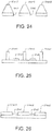
- the walls may be formed adjacent to the sensor chips on both sides as indicated by the walls 51hm2 in FIG. 26 .
- wall 51d, wall 51e, wall 51f, wall 51g, and wall 51h may be omitted, or only one of wall 51d, wall 51e, wall 51f, wall 51g, and wall 51h may be provided while the others are omitted.
- wall 51d and wall 51e may be connected together.
- wall 51f and wall 51g may be connected together.
- wall 51g and wall 51h may be connected together.
- wall 51ds, wall 51es, wall 51fs, wall 51gs, and wall 51hs may be omitted.
- mirrors described in the foregoing embodiments may be replaced by equivalent lenses.
- Mirrors may also be added to bend the optical path.
- the sensor may also be configured without color filters, and the sensor may be a monochrome sensor that does not differentiate colors.
Landscapes
- Engineering & Computer Science (AREA)
- Multimedia (AREA)
- Signal Processing (AREA)
- Physics & Mathematics (AREA)
- General Physics & Mathematics (AREA)
- Optics & Photonics (AREA)
- Environmental & Geological Engineering (AREA)
- Facsimile Scanning Arrangements (AREA)
- Facsimile Heads (AREA)
Abstract
Description
- The present invention relates to a scanner and method of generating scanning data.
- A scanner configured to read image segments that partially overlap on a main scanning line by means of sensor chips corresponding to the individual segments, and generate scanning data for the main scanning line by synthesizing scanning data from plural segments respectively read by the plural sensor chips, is known from the literature. See, for example,
JP-A-2013-131794 - When concave mirrors corresponding one-to-one to each segment are disposed to the optical path through which light from segments partially overlapping each other in the main scanning line of a document, light (referred to below as stray light) other than the intended light from the segments the concave mirrors are designed to reflect may be incident to the concave mirrors. If stray light is reflected by a concave mirror and incident to the sensor, the image quality of the scanning data drops.
- An objective of the present invention is to improve the image quality of scanning data.
- To achieve the foregoing objective, a scanner according to the invention has a first mirror having multiple concavities configured to reflect light from a document; a sensor configured to sense light reflected by a concavity of the first mirror; and a wall disposed to the first mirror and protruding from between the multiple concavities.
- The wall in this configuration can block unwanted light (stray light), that is, light other than light from the part of a document corresponding to each concavity, from reaching the sensor. As a result, stray light striking the sensor can be prevented, and a drop in image quality due to stray light can be prevented.
- Preferably in a scanner according to another aspect of the invention, the sensor includes multiple sensor chips corresponding one-to-one with the concavities of the first mirror; and light from a defined range of a main scanning line of the document is reflected by a first concavity of the first mirror and input to a first sensor chip corresponding to the first concavity, and is reflected by a second concavity of the first mirror and input to a second sensor chip corresponding to the second concavity.
- In this configuration, the area of the document on the main scanning line read by the first sensor chip, and the area read by the second sensor chip, overlap in part (the range of overlap is referred to as the defined range herein). This configuration can therefore generate scanning data for one main scanning line by synthesizing the scanning data in the range corresponding to the first sensor chip, and the scanning data in the range corresponding to the second sensor chip, based on the scanning data from the defined range.
- Preferably in a scanner according to another aspect of the invention, the first concavity and the second concavity are aligned adjacently in a main scanning direction; the sensor chips are aligned in the main scanning direction; and the wall protrudes from between the first concavity and the second concavity to a height Hdm equal to (0 < Hdm < L- (q + Wdm)/(2tan θ2)) where: L is a distance to the first mirror from a virtual plane, which is a position where an image formed through the first mirror on the sensor chip is in focus; q is the length of the defined range on the main scanning line in the virtual plane; θ2 is the angle, in a plane including a principal ray from an end of the defined range and the main scanning line, between a perpendicular to the main scanning line and the principal ray; and Wdm is a width in the main scanning direction of the wall disposed to a position equidistant from the first concavity and the second concavity.
- This aspect of the invention enables configuring a wall of a height that does not block at least the principal rays from the ends of the defined range.
- Preferably, a scanner according to another aspect of the invention also has a second mirror having multiple concavities, and configured to reflect to the sensor, by corresponding concavities, light reflected by the multiple concavities of the first mirror; and an aperture that is different from the walls and is positioned between the first mirror and the second mirror on the optical path.
- Separately from an aperture provided between the first mirror and second mirror for the purpose of adjusting the amount of light incident to the sensor, this configuration provides walls located on the document side of the aperture in the optical path for the purpose of keeping stray light from striking the first mirror. Stray light on the document side of the aperture is therefore blocked by the walls.
- Preferably, a scanner according to another aspect of the invention also has a second wall disposed to the second mirror and protruding from between multiple concavities of the second mirror.
- In addition to walls protruding from between the concavities of the first mirror, this configuration also has walls protruding from between the concavities of the second mirror. As a result, stray light can be blocked even more effectively.
- Preferably, a scanner according to another aspect of the invention also has a third mirror having multiple concavities configured to reflect light from the document to a concavity corresponding to the first mirror; and an aperture that is different from the walls and is positioned between the third mirror and the first mirror on the optical path.
- Separately from an aperture provided between the third mirror and first mirror for the purpose of adjusting the amount of light incident to the sensor, this configuration provides walls located on the sensor side of the aperture in the optical path for the purpose of keeping stray light from striking the first mirror. Stray light on the sensor side of the aperture is therefore blocked by the walls.
- Preferably, in a scanner according to another aspect of the invention, the walls are adjacent to concavities of the first mirror on both sides of the wall.
- Stray light is thereby blocked by the walls adjacent to concavities of the first mirror on both sides of the wall.
- Preferably, in a scanner according to another aspect of the invention, the walls protrude from a ridge between concavities of the first mirror.
- Because the bottom of the wall conforms to the shape of the ridge and the wall protrudes from the ridge without a gap therebetween, even if there is a gap, the wall can prevent stray light being incident to the concavity from the gap.
- Preferably, in a scanner according to another aspect of the invention, a protruding end of the wall is shaped conforming to the shape of the ridge formed by concavities of the first mirror.
- This configuration blocks stray light by a wall that is disposed between adjacent concavities and has a concave shape conforming to the shape (concave) of the ridge formed by adjacent concavities.
- To achieve the foregoing objective, another aspect of the invention is a scanning data generating method that is used by a scanner including a first mirror having multiple concavities configured to reflect light from a document, a sensor configured to sense light reflected by a concavity of the first mirror, and a wall disposed to the first mirror and protruding from between the multiple concavities; and includes steps of reading the document by the sensor and generating scanning data of the document.
- This method can block, by a wall, unwanted light (stray light), that is, light other than light from the part of a document corresponding to each concavity, from reaching the sensor. As a result, stray light striking the sensor can be prevented, and a drop in image quality due to stray light can be prevented.
- Other objects and attainments together with a fuller understanding of the invention will become apparent and appreciated by referring to the following description and claims taken in conjunction with the accompanying drawings.
- In order that the present invention may be more readily understood, embodiments thereof will now be described, by way of example only, with reference to the accompanying drawings, of which:
-
FIG. 1 is a block diagram of a scanner. -
FIG. 2 illustrates the configuration around the conveyance mechanism of the scanner. -
FIG. 3 illustrates the configuration of an optical system of the scanner. -
FIG. 4 schematically illustrates image reduction by the optical system. -
FIG. 5 describes data synthesis. -
FIG. 6 is an oblique view of the walls of the first mirror. -
FIG. 7 schematically illustrates the optical paths and walls. -
FIG. 8 is an oblique view describing the height of walls in the first mirror. -
FIG. 9 is an oblique view describing the height of walls in the first mirror. -
FIG. 10 is a plan view of the walls of an aperture member. -
FIG. 11 is a plan view of the walls of an aperture member. -
FIG. 12 is a plan view of the walls of an aperture member. -
FIG. 13 is a plan view of walls of a second mirror. -
FIG. 14 is a plan view of walls of a second mirror. -
FIG. 15 is a plan view of walls of a second mirror. -
FIG. 16 is a plan view of walls of a second mirror. -
FIG. 17 is a plan view of walls of a sensor substrate. -
FIG. 18 is a plan view of walls of a sensor substrate. -
FIG. 19 is a plan view of walls of a sensor substrate. -
FIG. 20 is a flow chart of the scanning process. -
FIG. 21 schematically illustrates another embodiment of the invention. -
FIG. 22 schematically illustrates another embodiment of the invention. -
FIG. 23 schematically illustrates another embodiment of the invention. -
FIG. 24 schematically illustrates another embodiment of the invention. -
FIG. 25 schematically illustrates another embodiment of the invention. -
FIG. 26 schematically illustrates another embodiment of the invention. - Preferred embodiments of the present invention are described below in the following order: (1) scanner configuration, (2) shield wall configuration, (2-1) walls of a first mirror, (2-2) walls of an aperture member, (2-3) walls of a second mirror, (2-4) walls of a sensor substrate, (3) scanning process, (4) other embodiments.
-
FIG. 1 is a block diagram of ascanner 1 according to this embodiment of the invention. Thescanner 1 includes acontroller 10,conveyance device 40,communicator 70, operatingunit 80,computer 90, and a 2-channel reading unit (including light sources, sensors, and optical units). Thecontroller 10 includes a recording medium not shown, and a processor that reads and executes a program from the recording medium. The processor may be a dedicated circuit device such as an ASIC embodied by circuits executing a specific process, or a CPU and ASIC that work together. - The
controller 10 controls parts of thescanner 1, and generates scanning data based on output from a reading unit. An operatingunit 80 includes an output unit that provides information to the user, and an input unit for receiving input from the user. Thecontroller 10 controls the operatingunit 80 to display on the output unit information for selecting scanning conditions and instructing scanning, for example. Based on output from the output unit, the user can select scanning conditions and input start-scanning commands. - When a start-scanning command is input, the
controller 10 controls parts of thescanner 1 to execute the operations for scanning a document (such as conveying the document). When scanning data is output from the reading unit by this operation, thecontroller 10 generates scanning data. - The
communicator 70 is a device for communicating with an external device (anexternal computer 90 in this example), and thecontroller 10 can send desired information to thecomputer 90 and receive instructions and information from thecomputer 90 via thecommunicator 70. - In this embodiment of the invention, when the
controller 10 produces scanning data, thecontroller 10 sends the scanning data through thecommunicator 70 to thecomputer 90. The scanning data may obviously be used in many ways, and may be stored on a recording medium not shown of thescanner 1, stored on a removable recording medium, or sent through thecommunicator 70 to a device other than thecomputer 90. - The
scanner 1 according to this embodiment has both an automatic document feeder (ADF) not shown, and a scanning platen, and documents are scanned at the scanning position regardless of which is used. Thescanner 1 according to this embodiment has a first reading unit and a second reading unit. The first reading unit can scan both moving documents (the front or first side) that are conveyed by the ADF, and stationary documents that are placed by the user directly on the scanning platen. The second reading unit can scan moving documents (the back or second side, the opposite side as the front), and cannot scan stationary documents. - The first reading unit includes, as shown in
FIG. 1 , afirst sensor 21, afirst light source 31, asub-scanning device 41, and a firstoptical system 51. Thesub-scanning device 41 is a device for moving thefirst sensor 21,first light source 31, and firstoptical system 51 bidirectionally in the sub-scanning direction. - The second reading unit includes, as shown in
FIG. 1 , asecond sensor 22, a secondlight source 32, and a secondoptical system 52, and does not have a device equivalent to thesub-scanning device 41. More specifically, thesecond sensor 22, secondlight source 32, and secondoptical system 52 are stationary inside thescanner 1. Light from the secondlight source 32 is emitted to a specific position in the conveyance path of the moving document, and light from the moving document passes through the secondoptical system 52 and is sensed by thesecond sensor 22 to image the document. - The
first sensor 21 andsecond sensor 22 comprise multiple sensor chips. Each sensor chip forms a line sensor, which is a sensor extending in one direction, and comprises numerous photoelectric conversion elements arrayed in the one direction. In this embodiment, each sensor chip has photoelectric conversion elements arranged in three rows, and a red (R), green (G), and blue (B) color filter is respectively disposed to the photoelectric conversion elements in each row. In this embodiment of the invention, the direction in which the rows of photoelectric conversion elements extend is perpendicular to the sub-scanning direction (the conveyance direction of a moving document). The direction in which the photoelectric conversion elements are arrayed is referred to as the main scanning direction. - The multiple sensor chips of the
first sensor 21 are disposed at a specific interval in the main scanning direction. - The multiple sensor chips of the
second sensor 22 are disposed adjacently in the main scanning direction, and the interval between adjacent photoelectric conversion elements in different sensor chips is the same as the interval between photoelectric conversion elements in a sensor chip at a different position. In thesecond sensor 22, therefore, the multiple sensor chips are arrayed adjacently, and effectively form a line sensor for scanning one line in the main scanning direction. - The
first light source 31 and secondlight source 32 each have a lamp that emits light to a scanning area (exposure position) in the conveyance path of the moving document. When a document is scanned as a stationary document, the exposure position moves in the sub-scanning direction. Light reflected from the object (a document or white calibration plate, for example) located at the exposure position is received by the sensor chips of thefirst sensor 21 orsecond sensor 22, and the sensor chips generate signals corresponding to the amount of light received by each photoelectric conversion element. - The
first sensor 21 andsecond sensor 22 have an analog front end, not shown. The analog front end includes a circuit that applies gain to the signals output by the photoelectric conversion elements according to the amount of light received, and an analog/digital conversion (ADC) circuit. The analog front end in this example also has a recording medium for recording information indicating the gain, and the analog front end, based on the gain information, adjusts the gain of the black level of thefirst sensor 21 andsecond sensor 22 to the lowest output value, and the white level to the highest output level. - Note that in this embodiment the
first light source 31 and secondlight source 32 are light sources that output white light. Because the photoelectric conversion element arrays of thefirst sensor 21 andsecond sensor 22 are equipped with RGB color filters, thefirst sensor 21 andsecond sensor 22 can generate RGB scanning data based on the light from a document exposed to white light. - The
conveyance device 40 is a mechanism that conveys documents. Theconveyance device 40 conveys the moving document to the position exposed to light from thefirst light source 31, and the position exposed to light from the secondlight source 32, and then conveys the moving document out from thescanner 1. -
FIG. 2 schematically illustrates the conveyance path of theconveyance device 40. The conveyance path comprises plastic members not shown forming the path of the moving document, and a moving document is conveyed through the conveyance path by opposingconveyance rollers FIG. 2 . The exposure positions on the conveyance path are indicated by the dotted lines, and one line in the main scanning direction (direction perpendicular to the X-axis and Z-axis) is read at the exposure position by thefirst sensor 21 andsecond sensor 22. - Light from the area of one line on a document is therefore split into light from multiple areas of which the ends in the main scanning direction overlap, and each of the split light beams is focused on a sensor chip. As a result, in this embodiment of the invention, the output from the sensor chips of the
first sensor 21 must be synthesized to generate one line of scanning data. A merging mark used as an index for synthesizing data is therefore formed on thecalibration plate 61 in this embodiment of the invention. - The merging mark is formed at a position where areas overlap at the ends of adjacent areas, and by scanning the merging mark when a document is not on the platen, the photoelectric conversion elements that read the same position can be identified in the output of the sensor chips.
- The
calibration plate 61 includes a white calibration plate and a black calibration plate for gain adjustment, the white level is determined based on the result measured with the white calibration plate, and the black level is determined based on the result measured with the black calibration plate. Note that thecalibration plate 61 may be configured with a moving part, and disposed so that the target selected from among the merging mark, white calibration plate, and black calibration plate is moved by the moving part and set to the exposure position. - Like
calibration plate 61,calibration plate 62 also has a white calibration plate and a black calibration plate. - In
FIG. 2 , thesub-scanning device 41 is a device capable of moving the first unit U1 bidirectionally in the sub-scanning direction (X-axis). When scanning a moving document, thesub-scanning device 41 sets the first unit U1 to a defined position as shown inFIG. 2 . The document is then scanned with the first unit U1 at this specific position. - When scanning a stationary document set on the scanning platen T (that is, when scanning on a flat bed), the
sub-scanning device 41 moves thefirst sensor 21,first light source 31, and firstoptical system 51 in the sub-scanning direction to scan the document. In the case of a stationary document, therefore, the area indicated inFIG. 2 by the dotted line and the dot-dash line connected to the dotted line is the exposure position (the document scanning range), and the exposure position can move in the sub-scanning direction. - The
second sensor 22, secondlight source 32, and secondoptical system 52 of the second reading unit are disposed in the second unit U2 shown inFIG. 2 . When scanning a moving document, one side (the front) is read by the first unit U1, and the other side (the back) is read by the second unit U2 when necessary. In this embodiment of the invention, the second reading unit (second unit U2) is a CIS (contact image sensor). - The first
optical system 51 includes an optical member (reduction optics system) for reducing and converging an image of the document on thefirst sensor 21. More specifically, the firstoptical system 51 has a member forming an optical path guiding, to the sensor chip, light from the document produced by thefirst light source 31 emitting light to the document. The optical path may be configured in many ways, and can be configured from combinations of various members, including an aperture member, lenses, and mirrors. -
FIG. 3 illustrates the firstoptical system 51 in this embodiment of the invention as viewed parallel to the main scanning direction. The configuration inFIG. 3 shows thefirst light source 31 that emits light to the document P, first optical system 51 (51a to 51h), and afirst sensor 21. - A first
optical system 51 uses configurations which include afirst mirror 51a with multiple concavities, asecond mirror 51b with multiple concavities, anaperture member 51c having multiple openings that function as apertures; and walls (51d to 51h) for blocking stray light; and guides the light to thesensor chip 21a by splitting the light from one line in the main scanning direction of the document P (the direction perpendicular to the X-axis and Z-axis) into multiple areas that overlap in part in the main scanning direction, and reducing the image of each area. - Note that in
FIG. 3 the light beam reflected from a desired area on the main scanning line (scan line) is indicated by the three lines. More specifically, the principal ray, which is the light ray in the center of the light beam, is indicated by a dot-dash line, and the rays on the outside of the light beam are indicated by the dot-dot-dash lines. -
FIG. 4 schematically illustrates the operation of the optical system with the main scanning direction on the horizontal axis. Because understanding would be complicated if the incident beam and outgoing beam overlapped, the concavity 51ai of thefirst mirror 51a, and the concavity 51bi of thesecond mirror 51b, are represented by ovals representing replacement by equivalent lenses with the outgoing beam leaving the lens from the opposite side from which the incident beam enters. As shown in the figure, there is a one-to-one correlation between the concavity 51ai of eachfirst mirror 51a and the aperture 51ci (opening) of the correspondingaperture member 51c. The concavities 51ai of thefirst mirrors 51a and the concavities 51bi of thesecond mirrors 51b also correspond one-to-one. Thesensor chips 21a of thefirst sensor 21 are provided on asubstrate 210. - In
FIG. 4 , light from the document P passes the firstoptical system 51 and is guided to thesensor chip 21a, and the path of light from the document P is indicated schematically by the dotted lines and dot-dash lines. In other words, thesensor chip 21a extends in the main scanning direction (Y-axis), and images of adjacent parts of the document P that partially overlap in the main scanning direction are reduced in the parts of the firstoptical system 51 corresponding to those parts of the document P. The images from each area of the document P are then focused on thesensor chip 21a corresponding to those parts. More specifically, an image of the area of length LP in the main scanning direction is focused on asensor chip 21a of length d. - One-to-one imaging optics that form images on the
second sensor 22 without reducing the size are used in the secondoptical system 52. Thecontroller 10 therefore does not need to apply the synthesizing process to the output of thesecond sensor 22, and applies another imaging process (such as cropping or edge enhancement) to acquire the scanning data. - However, because the
first sensor 21 reads the same positions on the document P multiple times, thecontroller 10 must synthesize data output from adjacent sensor chips where the outputs coincide to generate the scanning data. More specifically, thecontroller 10, based on the read results of the merging mark formed on thecalibration plate 61, superimposes the outputs of thesensor chips 21a. More specifically, as shown inFIG. 4 , thefirst sensor 21 is embodied bymultiple sensor chips 21a, and themultiple sensor chips 21a are disposed at different positions. - When the same positions are read by
different sensor chips 21a, the same positions are read at the ends of thesensor chips 21a. Because these same positions are where the merging marks are disposed on thecalibration plate 61, when the merging mark is read without a document present, eachsensor chip 21a outputs data capturing the merging mark. -
FIG. 5 schematically illustrates the photoelectric conversion elements of thesensor chip 21a, the black dots denoting the photoelectric conversion elements. InFIG. 5 , the merging mark is a line extending in the sub-scanning direction, and the areas around the merging mark are white. - The merging mark is read by each pair of
adjacent sensor chips 21a. InFIG. 5 , the photoelectric conversion elements of thesensor chips 21a that read the merging mark are indicated by black dots, the merging mark is indicated by hatching, and the photoelectric conversion elements that read the merging mark are shown overlapping. One of theadjacent sensor chips 21a is located on the top left side, the other is located on the bottom right side, and thesensor chips 21a are shown schematically so that the photoelectric conversion elements that read the merging mark are vertically aligned. One of the twoadjacent sensor chips 21a is referred to below as first sensor chip 21a1, and the other as second sensor chip 21a2. - The first sensor chip 21a1 and second sensor chip 21a2 output, as serial data, signals corresponding to the amount of light detected by the photoelectric conversion elements aligned in the main scanning direction. In this example, the
controller 10 analyzes the output of the first sensor chip 21a1, and determines that the merging mark was detected by the fifth and sixth photoelectric conversion elements E5, E6 from the end. Thecontroller 10 also analyzes the output of the second sensor chip 21a2, and determines that the merging mark was detected by the fourth and fifth photoelectric conversion elements E4, E5 from the end. In this case, thecontroller 10 determines that the fifth and sixth photoelectric conversion elements E5, E6 of the first sensor chip 21a1, and the fourth and fifth photoelectric conversion elements E4, E5 of the second sensor chip 21a2, read the same position, and in memory not shown stores the locations of the corresponding elements in eachsensor chip 21a. - The
controller 10 applies the above process sequentially from the end of thesensor chips 21a in the main scanning direction, and identifies the location of the photoelectric conversion elements that read the same position in eachsensor chip 21a. Note that of themultiple sensor chips 21a embodying thefirst sensor 21, any of the sensor chips other than the sensor chips at the ends may be either a first sensor chip 21a1 or a second sensor chip 21a2. - For example, if one
sensor chip 21a is the first sensor chip 21a1 and then becomes the adjacent second sensor chip 21a2 such that the second sensor chip 21a2 is treated as the first sensor chip 21a1, thesensor chip 21a adjacent thereto on the opposite side becomes the second sensor chip 21a2. - Once the locations of the photoelectric conversion elements reading the same position are determined as described above, the next time a document P is scanned, the
controller 10 generates one line of scanning data by synthesizing the outputs of thesensor chips 21a based on their respective positions. - The first
optical system 51 has walls (51d to 51h) for preventing stray light, which is light other than the light on the optical paths shown inFIG. 3 andFIG. 4 , from being incident to thesensor chips 21a. -
Walls 51d shown inFIG. 3 are shield walls disposed on thefirst mirror 51a. As shown inFIG. 6 ,walls 51d include walls 51dm, and walls 51ds connecting one wall 51dm with the adjacent wall 51dm. The walls 51dm are disposed adjacent to two adjacent concavities. The walls 51dm protrude from the ridge line R between two adjacent concavities, and there is no gap between the ridge line R and the walls 51dm (the bottom of the wall 51dm is in contact with the ridge line R). In other words, the walls 51ds from a grid pattern (or a ladder shape) when seen from the Z-axis, and one concavity can be seen from one opening between walls 51ds. The protruding distal ends To of the walls 51dm have a concave shape conforming to the shape of the ridge line R. The walls 51ds and walls 51dm surround the edges of the concavity 51ai. By connecting the walls 51ds and walls 51dm, the strength of the walls 51dm increases, and the angle of the walls 51dm to the optical path is stabilized. - The shape (wall thickness and height) of the walls 51dm is described below with reference to
FIG. 7 . -
FIG. 7 schematically illustrates the configuration of the walls on the optical path through which light reflected from the document P is guided to asensor chip 21a. Of the multiple concavities of thefirst mirror 51a, the target concavity is referred to as the first concavity 51a1, and the concavity adjacent to the first concavity 51a1 is referred to as the second concavity 51a2. InFIG. 7 , the concavity of thefirst mirror 51a and the concavity of thesecond mirror 51b are represented by convex lenses. - In
FIG. 7 , the light beam (conical shapes) representing light reflected from a desired position on the main scanning line (scan line) of the document P are indicated by the three lines (the principal ray, which is the light ray in the center of the light beam, indicated by a dot-dash line, and the rays on the outside of the light beam indicated by the dot-dot-dash lines). - The thickness (width Wdm) of the walls 51dm in this example is constant, and the wall 51dm between a first concavity 51a1 and a second concavity 51a2 is disposed at a position equidistant from the first concavity 51a1 and second concavity 51a2.
- Light reflected from range P1 (the range from end P1L to end P1R) on the main scanning line of the document P is incident to the first sensor chip 21a1 through the first concavity 51a1 of the
first mirror 51a, the first aperture 51c1, and the first concavity 51b1 of thesecond mirror 51b. - Light reflected from range P2 (the range from end P2L to end P2R) on the main scanning line of the document P is incident to the second sensor chip 21a2 through the second concavity 51a2 of the
first mirror 51a, the second aperture 51c2, and the second concavity 51b2 of thesecond mirror 51b. - The overlapping portions (referred to below as the defined range) of the range P1 and second range P2 are read by both the first sensor chip 21a1 and the second sensor chip 21a2.
- The length of the defined range in the main scanning direction is length q.
- Light reflected from the end P1R of the defined range on the second concavity 51a2 side is incident to the first sensor chip 21a1 at end S1L of the first sensor chip 21a1 (the end farthest from the second sensor chip 21a2).
- Light reflected from the end P2L of the defined range on the first concavity 51a1 side is incident to the second sensor chip 21a2 at the photoelectric conversion element at the end S2R of the second sensor chip 21a2 farthest from the first sensor chip 21a1.
- Note that light reflected from end P1R of the defined range is incident to the photoelectric conversion element on the opposite end of the first sensor chip 21a1 as end S2R of the second sensor chip 21a2; and light reflected from end P2L of the defined range is incident to the photoelectric conversion element on the opposite end of the second sensor chip 21a2 as end S1L of the first sensor chip 21a1.
- When a wall 51dm is not disposed between the concavities of the
first mirror 51a, some of the light reflected by the second concavity 51a2 of thefirst mirror 51a passing through the adjacent first aperture 51c1 instead of the second concavity 51a2 of thefirst mirror 51a may not be preventable, possibly resulting in a drop in image quality due to stray light. However, this problem can be prevented by the walls 51dm. While the height of the walls 51dm is preferably as great as possible to prevent this problem from occurring, the following limits can be defined to ensure that light from the imaging areas (range P1 and second range P2, for example) on the main scanning line defined for each concavity is reflected by the target concavity. - More specifically, if the target is first concavity 51a1, the wall height must be limited to a height at which at least the principal ray from the end P1R on the second concavity 51a2 side of the defined range where range P1 and second range P2 overlap is not blocked. Therefore, the wall 51dm disposed between the first concavity 51a1 and second concavity 51a2 of the
first mirror 51a protrudes from point p02 on the ridge line R to height Hdm defined by equation (1).
- In equation (1), L is the distance from a virtual plane, which is the position where the image formed through the
first mirror 51a on thesensor chip 21a is in focus, to thefirst mirror 51a. The relative positions of the scanning platen T (not shown inFIG. 7 ) and firstoptical system 51 are designed so that the document P is positioned on this virtual plane. The following description supposes that the read side of the document P is position on this virtual plane. More specifically, length L is the distance from point p02 to the document P end P1R on a plane parallel to the XZ plane. - Note that as shown in
FIG. 6 , thefirst mirror 51a is disposed extending in the main scanning direction (Y-axis), and the walls 51dm protrude from the ridge line R of thefirst mirror 51a in the direction parallel to the XZ plane. - Point p02 is described below with reference to
FIG. 8 andFIG. 9 . -
FIG. 8 is an oblique view of thefirst mirror 51a omitting for clarity the wall 51ds shown on the -X-axis side in the oblique view inFIG. 6 .FIG. 9 schematically illustrates the wall 51dm between the first concavity 51a1 and the second concavity 51a2 as seen from the -Y-axis side to the +Y-axis side. - Point p01 is the point where the principal ray Rc of the light reflected from the second concavity 51a2 side end P1R (see
FIG. 7 ) of the defined range, which is where range P1 and second range P2 overlap, is incident to the first concavity 51a1. The principal ray Rc from end P1R projected to the side (a plane parallel to the XZ plane) of the wall 51dm on the first concavity 51a1 side is ray Rcc as shown inFIG. 9 . Point p02 is at the intersection of ray Rcc and the ridge line (seeFIG. 8 andFIG. 9 ) on the first concavity side of the ridge line R formed by the first concavity 51a1 and second concavity 51a2. - As shown in
FIG. 7 , θ2 in equation (1) is the angle, in a plane including the main scanning line of the document P and the principal ray Rc incident to the first concavity 51a1 from end P1R, between the perpendicular to the main scanning line and the principal ray Rc. - Wdm is the width in the main scanning direction (Y-axis) of the wall 51dm located equidistantly from the first concavity 51a1 and second concavity 51a2. Point p05 is the intersection between ray Rcc and principal ray Rc. Note that the Y coordinate of the center of the length q of the defined range on the Y-axis, and the Y coordinate of the center of the wall 51dm on the Y-axis, are the same, and wall 51dm is parallel to the XZ plane. Therefore, (q + Wdm)/(2tanθ2) in equation (1) means the length of line k1. As shown in
FIG. 9 , therefore, the wall 51dm is formed so that the length (height Hdm) from point p02 parallel to the ray Rcc is less than (L - k1). By making the height Hdm of the wall 51dm less than (L - k1), the wall 51dm can be configured to not obstruct at least the principal ray Rc incident to the first concavity 51a1 from the end P1R of the defined range. - If at least the principal ray Rc in the light beam incident to the first concavity 51a1 side from the end P1R is not blocked by the wall 51dm, data can be synthesized using the merging mark even if ray Re on the outside side of the light beam from the principal ray Rc and closest to the second concavity 51a2 side are blocked by the wall 51dm. More specifically, data can be synthesized using a merging mark in scanning data with a reduced amount of light around the merging mark. In addition, because the light beam of the reflected light from the end P1R detected by the second sensor chip 21a2 includes rays on the outside side of the principal ray, the image quality of scanning data after synthesis of the position at the end P1R is not affected. Note that the height Hdm of the wall 51dm from point p02 can be set to a height not obstructing ray Re if height Hdm satisfies equation (2) below.

- As shown in
FIG. 7 , in equation (2), θ1 is the angle, in a plane (the same plane as the plane including the main scanning line and principal ray Rc) including the main scanning line of the document P and the ray Re closest to the second concavity 51a2 side of the light beam incident to the first concavity 51a1 from end P1R, between the perpendicular to the main scanning line and the principal ray Re. - Point p04 is the intersection of ray Rcc (ray Re from end P1R projected to the side (a plane parallel to the XZ plane) of the wall 51dm on the first concavity 51a1 side) and ray Re. In equation (2), (q + Wdm)/(2tanθ2) means the length of line k2.
- Note that in
FIG. 7 to FIG. 9 , wall 51dm is formed so that the height Hdm from point p02 satisfies equation (2). More specifically, the figures show a wall 51dm of Hdm < L - k2. - The other walls 51dm of the
first mirror 51a are formed in the same way as the wall 51dm between the first concavity 51a1 and second concavity 51a2. - Note that the walls 51ds joining the walls 51dm are disposed in contact with the sub-scanning direction (X-axis) edges of the concavities between one wall 51dm and the next wall 51dm. There is no gap between the X-axis end of a concavity and the wall 51ds. The wall 51ds may be formed to any height not blocking the beam of the light incident to the concavities and the beam of light reflected from the concavities; and the height of walls 51ds on the side of light incident to the concavities and the height of walls 51ds on the side of light outgoing from the concavities may be the same or different. In this embodiment of the invention, as shown in
FIG. 6 , the walls 51ds on the side of the incident light are higher than the walls 51ds on the side of outgoing light. - As described above, unintended light (stray light) from outside the targeted range of the main scanning line corresponding to the concavities of the
first mirror 51a can be blocked by the walls 51dm disposed between one concavity and the adjacent concavity. As a result, stray light being picked up by thesensor chip 21a can be prevented, and a drop in the image quality of scanning data due to stray light can be prevented. - The
walls 51e andwalls 51f disposed to anaperture member 51c as shown inFIG. 3 are described next. - An
aperture member 51c is a flat member extending in the main scanning direction (Y-axis), and a plurality of apertures (openings) are formed in the main scanning direction. As shown inFIG. 7 , the aperture corresponding to the first concavity 51a1 is referred to as the first aperture 51c1, and the aperture corresponding to the second concavity 51a2 is referred to as the second aperture 51c2.FIG. 10 shows theaperture member 51c from the document P side of the optical path.FIG. 11 is a section view through f11- f11 inFIG. 10 , andFIG. 12 is a section view through f12 - f12 inFIG. 10 . -
Walls 51e are shield walls protruding from theaperture member 51c to the document P side of the optical path, and as shown inFIG. 10 , include walls 51em disposed between the multiple apertures formed in theaperture member 51c, and walls 51es joining one wall 51em to another wall 51em. By connecting walls 51es by a pair of walls 51em, the strength of the walls 51em is increased and the angle of the walls 51em to the surface of theaperture member 51c is stable. - Likewise,
walls 51e are shield walls protruding from theaperture member 51c to the sensor chip side of the optical path, and like thewalls 51e shown inFIG. 10 , include walls 51fm disposed between the multiple apertures, and walls 51fs joining one wall 51fm to another wall 51fm. By connecting walls 51fs by a pair of walls 51fm, the strength of the walls 51fm is increased and the angle of the walls 51fm to the surface of theaperture member 51c is stable. - As shown in
FIG. 11 , the walls 51em disposed on opposite sides of the first aperture 51c1 protrude from theaperture member 51c to a height and position not blocking the principal rays Rc (in this example, the two principal rays incident to the photoelectric conversion elements at both ends in the main scanning direction of the first sensor chip 21a1 corresponding to the first aperture 51c1). - As shown in
FIG. 11 , the walls 51em may also be disposed to a height Hem and position not blocking the outside-most rays Re, in addition to the principal rays Rc in the light beam incident to the photoelectric conversion elements at both ends in the main scanning direction of the first sensor chip 21a1. The other walls 51em disposed to theaperture member 51c are also disposed with the same shape described above. - As shown in
FIG. 12 , the walls 51es connecting one wall 51em to another wall 51em are disposed to a height Hes not obstructing light beams incident to the corresponding sensor chip (first sensor chip 21a1 in this example). The other walls 51es disposed to theaperture member 51c are also disposed with the same shape described above. - The walls 51fm disposed on opposite sides of the first aperture 51c1 protrude from the
aperture member 51c to a height and position not blocking the principal rays Rc incident to the ends of the first sensor chip 21a1 in the main scanning direction. - As shown in
FIG. 11 , the walls 51fm may also be disposed to a height Hfm and position not blocking the rays Re closest to the second aperture 51c2, in addition to the principal rays Rc in the light beam incident to the first sensor chip 21a1. The other walls 51fm disposed to theaperture member 51c are also disposed with the same shape described above. - As shown in
FIG. 12 , the walls 51fs connecting one wall 51fm to another wall 51fm are disposed to a height Hfs not obstructing light beams incident to the corresponding sensor chip (first sensor chip 21a1 in this example). The other walls 51fs disposed to theaperture member 51c are also disposed with the same shape described above. - As a result, a drop in the image quality of scanning data due to stray light can be prevented by disposing
walls 51e andwalls 51f on theaperture member 51c. - If walls 51em are not disposed on the document P side between one aperture and the adjacent aperture, reflected light from a concavity (such as second concavity 51a2) other than the first concavity 51a1 of the
first mirror 51a corresponding to the first aperture 51c1 cannot be prevented from passing through the first aperture 51c1, and a drop in image quality due to stray light may result. - In addition, if walls 51fm are not disposed on the sensor side between adjacent apertures, some light that passed the first aperture 51c1 being incident to a concavity (such as second concavity 51b2) other than the first concavity 51b1 of the
second mirror 51b corresponding to the first aperture 51c1 cannot be prevented, and a drop in image quality due to stray light may result. - However, these problems can be prevented by disposing walls 51em and walls 51fm to the
aperture member 51c. - The
walls 51g disposed to thesecond mirror 51b (seeFIG. 3 ) are described next. - The
second mirror 51b has multiple concavities, and reflects light reflected from the multiple concavities of thefirst mirror 51a by the corresponding concavities to thecorresponding sensor chip 21a.FIG. 13 illustrates the surface on which the concavities of thesecond mirror 51b are formed. Shown inFIG. 13 are the first concavity 51b1 corresponding to the first aperture 51c1, and the second concavity 51b2 corresponding to the second aperture 51c2.FIG. 14 is a section view through line f14-f14 inFIG. 13 ,FIG. 15 is a section view through line f15-f15 inFIG. 13 , andFIG. 16 is a section view through line f16-f16 inFIG. 13 . - As shown in
FIG. 13 ,walls 51g include walls 51gm (examples of second walls) disposed between adjacent concavities of thesecond mirror 51b, and walls 51gs connecting adjacent walls 51gm. A wall 51gm disposed between a first concavity 51b1 and a second concavity 51b2 is disposed adjacent to the concavity on each side. - The walls 51gm protrude from the ridge line R formed by the first concavity 51b1 and second concavity 51b2, and there is no gap between the ridge line R and the wall 51gm. The protruding distal end To of the wall 51gm is concave, following the shape of the ridge line R as shown in
FIG. 16 . - The walls 51gs enclose the edges of the walls 51gm, first concavity 51b1, and second concavity 51b2. By the walls 51gs connecting the walls 51gm, the strength of the walls 51gm is improved, and the angle of the walls 51gm to the optical path is stable.
- In
FIG. 14 , the thin dot-dash lines indicate the principal ray in the beam of incident light passing through the corresponding aperture and incident to a concavity of thesecond mirror 51b, and the thin dot-dot-dash lines indicate rays on the outside side of the light beam. - Also in
FIG. 14 , the bold dot-dash lines indicate the principal ray in the beam of reflected light from a concavity of thesecond mirror 51b to thecorresponding sensor chip 21a, and the bold dot-dot-dash lines indicate rays on the outside side of the light beam. - The walls 51gm disposed on both sides of the first concavity 51b1 are configured in a shape protruding from the ridge line R in a shape (height Hgm, width Wgm) not interfering with the principal rays of the light beams incident to the photoelectric conversion elements located at the opposite ends in the main scanning direction (Y-axis) of the first sensor chips 21a1 corresponding to the first concavity 51b1.
- In
FIG. 15 , the thin dot-dash lines indicate the principal ray in the beam of incident light passing through the first aperture 51c1 corresponding to the first concavity 51b1 and incident to the first concavity 51b1, and the thin dot-dot-dash lines indicate rays on the outside side of the light beam. - Also in
FIG. 15 , the bold dot-dash lines indicate the principal ray in the beam of reflected light from the first concavity 51b1 to thecorresponding sensor chip 21a, and the bold dot-dot-dash lines indicate rays on the outside side of the light beam. - As shown in
FIG. 15 , the walls 51gs connecting one wall 51gm to another wall 51gm are disposed on thesecond mirror 51b to a height Hgs at which the wall 51gs that will not block the beam of incident light to the concavity of thesecond mirror 51b and the beam of reflected light from the concavity. - As described above, by disposing walls 51gm between adjacent concavities of the
second mirror 51b, a drop in image quality in the scanning data due to stray light can be prevented. - If walls 51gm are not provided between the concavities of the
second mirror 51b, some of the light reflected from the first concavity 51b1 being incident to a sensor chip (such as the second sensor chip 21a2) other than the first sensor chip 21a1 corresponding to the first concavity 51b1 cannot be prevented, and a drop in image quality due to stray light may result. - However, this problem can be prevented by providing walls 51gm on the
second mirror 51b. - The
walls 51h (seeFIG. 3 ) disposed on thesubstrate 210 on which thesensor chips 21a are disposed are described next. -
FIG. 17 is a plan view of thesubstrate 210.FIG. 18 is a section view through line f18-f18 inFIG. 17 , andFIG. 19 is a section view through line f19-f19 inFIG. 17 . As shown inFIG. 17 , thewalls 51h include walls 51hm disposed between themultiple sensor chips 21a arrayed parallel to the main scanning direction on thesubstrate 210; and walls 51hs connecting the walls 51hm. Onesensor chip 21a is surrounded by a pair of walls 51hm and a pair of walls 51hs. - In
FIG. 18 and FIG. 19 , the dot-dash lines indicate the principal rays in the beam of incident light from thesecond mirror 51b to thesensor chip 21a, and the dot-dot-dash lines indicate rays on the outside side of the light beam. - As shown in
FIG. 18 , the walls 51hm are configured in a shape not interfering with the principal rays of the light beams incident to the photoelectric conversion elements located at both ends in the main scanning direction of thecorresponding sensor chip 21a. More specifically, in this embodiment of the invention, the walls 51hm are formed perpendicularly to thesubstrate 210, and the principal rays incident from the inside to the outside of thesensor chip 21a at the Y-axis ends of thesensor chip 21a are not blocked by the walls 51hm. - As shown in
FIG. 19 , the walls 51hs connecting one wall 51hm to the other wall 51hm are configured to a height Hhs not interfering with the light beam incident to the first sensor chip 21a1. Note that RGB photoelectric conversion elements that receive light from the same position on the main scanning line of the document P are disposed to the imaging area S3 of the light beam shown inFIG. 19 . - As described above, by disposing walls 51hm protruding from the
substrate 210 between thesensor chips 21a on thesubstrate 210, a drop in image quality in the scanning data due to stray light can be prevented. - If walls 51hm are not provided, some of the light reflected from a concavity (such as the second concavity 51b2) other than the first concavity 51b1 of the
second mirror 51b corresponding to the first sensor chip 21a1 being incident to the first sensor chip 21a1 cannot be prevented, and a drop in image quality due to stray light may result. - However, this problem can be prevented by providing walls 51hm to the
substrate 210. - The scanning process in this embodiment of the invention is described next with reference to the flow chart in
FIG. 20 . - When the user directly or indirectly selects the document scanning resolution and paper feed method (ADF or document platen), and commands scanning to start, the
controller 10 receives the scan command and starts the scanning process shown inFIG. 20 . When the scanning process starts, thecontroller 10 gets the scanning settings, including the document scanning resolution and the paper feed method (step S100). Note that in this example the user can select and set the desired resolution from among the plural document scanning resolutions that can be set for reading light reflected from a moving document. - Next, the
controller 10 measures image shading. More specifically, the lowest level of light detectable by the sensor chip is the black level, and the highest level of detectable light is the white level, but the black level and white level can vary according to the sensor, light source, and other characteristics. For example, sensor characteristics may vary due to noise such as dark current, sensor manufacturing errors, and aging, and the black level and white level can vary according to such variations. Therefore, to scan with high quality, imaging shading is preferably measured before reading a document to determine at least one of the black level and white level. - The
controller 10 in this example first measures the white level (step S105). More specifically, before reading the document, thecontroller 10 controls the first reading unit (and the second reading unit if scanning both sides) to read the white calibration plate of thecalibration plate 61. As a result, because output indicating the measurement acquired by the first sensor 21 (and thesecond sensor 22 if scanning both sides) from the white calibration plate is acquired, thecontroller 10 acquires the output as the white level. - Next, the
controller 10 measures the black level (step S110). More specifically, before reading the document, thecontroller 10 controls the first reading unit (and the second reading unit if scanning both sides) to read the black calibration plate of thecalibration plate 61. As a result, because output indicating the measurement acquired by the first sensor 21 (and thesecond sensor 22 if scanning both sides) from the black calibration plate is acquired, thecontroller 10 acquires the output as the black level. - Next, the
controller 10 measures the merging mark (step S115). More specifically, before scanning the document, thecontroller 10 controls the first reading unit to scan the merging mark of thecalibration plate 61. As a result, the results of scanning the merging mark are output from the multiple sensor chips of thefirst sensor 21. Note that because there is no need to synthesize the output of thesecond sensor 22 in this embodiment, the merging mark is not scanned by thesecond sensor 22. - Next, the
controller 10 identifies the photoelectric conversion elements that read the same position (step S120). For example, using the example inFIG. 5 , thecontroller 10 identifies photoelectric conversion elements E5, E6 of the first sensor chip 21a1, and photoelectric conversion elements E4, E5 of second sensor chip 21a2, as the photoelectric conversion elements that read the same position. Thecontroller 10 executes the same process for eachsensor chip 21a, and identifies the photoelectric conversion elements in each sensor chip that read the same position. - Next, the
controller 10 sets the black level and white level (step S125). That is, thecontroller 10, based on the white level measured in step S105 and black level measured in step S110, sets the white level and black level for each photoelectric conversion element. More specifically, based on the white level measured in step S105 and black level measured in step S110, the control unit 13 sets the gain to enable measuring gradations between the white level and black level in the effective detection range. - Next, the
controller 10 determines if the paper supply method is by ADF or not (step S130). More specifically, thecontroller 10 references the scanning settings acquired in step S100 to determine if the paper supply method is by ADF or using the scanning platen. If thecontroller 10 determines in step S130 that the paper supply method is not by ADF, that is, that a document on the document platen is to be scanned, thecontroller 10 starts sub-scanning (step S135). More specifically, thecontroller 10 outputs a control signal to thesub-scanning device 41 to move thefirst sensor 21,first light source 31, and firstoptical system 51 in the sub-scanning direction. - The
controller 10 reads the document during the sub-scanning operation (step S140). More specifically, thecontroller 10 controls thefirst sensor 21 to read, and acquires the read results from thesensor chips 21a of thefirst sensor 21. - Next, the
controller 10 signal processes the output from thesensor chips 21a (step S145). More specifically, thecontroller 10 digitizes the output of thesensor chips 21a, adjusts the gain according to the white level and black level set in step S125, executes a synthesizing process causing the photoelectric conversion elements identified in step S120 to output one pixel, converts value and color, crops the document, applies edge enhancement, and executes other signal processing operations. These processes may be applied sequentially to the line by line results read in step S140, or in a batch after all read results are acquired. - Next, the
controller 10 outputs the scanning data (step S150). More specifically, when one page of data synthesized in step S145 is accumulated, thecontroller 10 generates scanning data for the one page, and outputs the scanning data through thecommunicator 70 to thecomputer 90. - If the
controller 10 determines in step S130 that the paper supply method is by ADF, thecontroller 10 starts conveying the document (step S155). More specifically, thecontroller 10 outputs a control signal to thesub-scanning device 41 to move the first reading unit to a specific scanning position. Thecontroller 10 then outputs a control signal to theconveyance device 40 to convey the document through the conveyance path. - While the document is being conveyed, the
controller 10 reads the document (step S160). More specifically, thecontroller 10 controls thefirst sensor 21 to read, and acquires the read results from thesensor chips 21a of thefirst sensor 21. Note that if duplex scanning is selected in step S100, thecontroller 10 also controls thesecond sensor 22 to read, and acquires the read results from thesecond sensor 22. - Next, the
controller 10 signal processes the output (step S165). More specifically, thecontroller 10 digitizes the output of thesensor chips 21a (including the output from thesecond sensor 22 if duplex scanning is selected), adjusts the gain according to the white level and black level set in step S125, executes a synthesizing process causing the photoelectric conversion elements identified in step S120 to output one pixel, converts value and color, crops the document, applies edge enhancement, and executes other signal processing operations. These processes may be applied sequentially to the line by line results read in step S160, or in a batch after all read results are acquired. Note that because there is no need to synthesize the read results from thesecond sensor 22, the read results from thesecond sensor 22 are not subject to the synthesis process. - Next, the
controller 10 outputs the scanning data (step S170). More specifically, when one page of data synthesized in step S165 is accumulated, thecontroller 10 applies image processing including cropping and edge enhancement, for example, generates scanning data for the one page, and outputs the scanning data through thecommunicator 70 to thecomputer 90. If duplex scanning was selected, thecontroller 10 generates the scanning data using the one page of data synthesized in step S165 and the one page of data read from the back in step S160, and then outputs to thecomputer 90. - The invention is described with reference to desirable embodiments above, but the invention is not so limited and can be varied in many ways. For example, the scanner described above may be a component of a multifunction device, which is an electronic device that is also used for other purposes.
- The merging mark may also be configured in many ways, and may be two lines or graphic of another shape. During synthesis, images may also be synthesized to eliminate deviation (such as skewing) of the sensor chips in the sub-scanning direction.
- To superimpose the outputs of photoelectric conversion elements that read the same part of the document, a statistical value (such as the average) of scanning data from one sensor chip and scanning data from the other sensor chip may be acquired and used, or the scanning data from one of the sensor chips may be used.
- Scanning data generated by scanning may be output to a
computer 90, output and stored to a storage medium such as USB memory installed to the device, output to a print mechanism and printed (or copied), or output and displayed on a monitor. - Alternatively, the final scanning data may be generated by outputting an area detection image to a
computer 90, and applying image analysis and synthesis by a driver program or application program of thecomputer 90. In this configuration, thecomputer 90 may be considered part of the scanner. - The first mirror may have multiple concavities reflecting light from the document. More specifically, the first mirror may be configured as needed to form an optical path to the sensor group by changing the direction of travel of light from a document by reflection. The light from a document may be any light output from the document as a result of exposing the document to light from a light source, and in many configurations is reflected light, but may be fluorescent light, for example.
- The first mirror has multiple concavities. More specifically, different optical paths can be formed by the concavities, and light from a document can be guided through multiple optical paths to multiple sensor chips corresponding to the respective optical paths.
- In addition, the concavities may be configured as surfaces that reflect and converge parallel incident light on a focal point, and may be surfaces configured as an optical system (such as a reduction optical system that reduces the size of the image) that changes the size of the image corresponding to the light from a document.
- The number of concavities is not limited insofar as the configuration at least guides light from multiple areas in the main scanning direction to multiple sensor chips. For example, a configuration that is a number corresponding to the number of sensor chips in a sensor can be used.
- In addition, multiple mirrors may be disposed to the same optical path. For example, a configuration that converges light through two reflections by two concavities may be used. The focal length and curvature of a concavity is not specifically limited, and may be changed according to the size of the scanner or the configuration of the optical system, for example.
- A sensor may include multiple sensor chips each having a photoelectric conversion element line that senses light reflected by a concavity. In other words, a sensor may be configured in any form enabling multiple sensor chips to read light reflected by multiple concavities. A photoelectric conversion element line of multiple photoelectric conversion elements is formed in each of the multiple sensor chips, and the direction in which the photoelectric conversion elements are arranged is the main scanning direction.
- Note that the sensor chip has photoelectric conversion elements arranged at least in the main scanning direction, and may also have photoelectric conversion elements at multiple positions in the sub-scanning direction. In the latter case, photoelectric conversion elements may be at multiple positions in the sub-scanning direction in the sensor chip, or by arraying sensor chips in the sub-scanning direction, photoelectric conversion elements may be disposed at multiple positions in the sub-scanning direction.
- Note that in a configuration in which photoelectric conversion elements are at multiple positions in the sub-scanning direction, the photoelectric conversion elements at multiple positions in the sub-scanning direction may be used to form images of different colors, or be used to form an image of one line in the main scanning direction by combining their outputs.
- The aperture member is disposed between the first mirror and the sensor in the optical path of light reflected by a concavity, and there may be multiple apertures paired one-to-one with the concavities. More specifically, any configuration that has an aperture disposed to each optical path of light reflected by each concavity, and focuses the light on the sensor chip after the light on the optical path is collimated by the aperture, may be used. An aperture corresponds one-to-one with a concavity. As a result, while there is always an aperture corresponding to a concavity, multiple concavities may correspond to each aperture. For example, a configuration that has multiple concavities on an optical path, and uses a single aperture to focus light from multiple concavities on the sensor chip, is conceivable.
- The sensor detecting light guided by a reduction optics system may be configured in any form enabling sensing light reflected by a concavity of a first mirror. For example, as described in the foregoing embodiments, the sensor may comprise multiple sensor chips arrayed in the main scanning direction, or comprising a single line sensor disposed lengthwise parallel to the main scanning direction.
- Note that a configuration having a third mirror with multiple concavities that reflect light from a document to a concavity corresponding to the first mirror, and an aperture different from the walls disposed to the optical path between the third mirror and the first mirror, is conceivable. In this configuration, the
second mirror 51b in the foregoing embodiment may be understood as equivalent to a first mirror, and thefirst mirror 51a in the foregoing embodiment as equivalent to a third mirror. - Furthermore, the foregoing embodiment describes a configuration having the walls disposed between the concavities of the first mirror, and the walls disposed between the concavities of the second mirror, adjacent to concavities on both sides of the wall, but may be configured in other ways insofar as the they are disposed to a height not blocking the principal rays of light reflected from the ends of the defined range.
- As shown in
FIG. 21 , for example, the walls 51gm may be disposed separated from the concavities 51bi on both sides. Alternatively, as shown inFIG. 22 , a wall 51gm1 that functions as a shield wall for the first concavity 51b1, and a separate wall 51gm2 that functions as a shield wall for the second concavity 51b2, may be disposed between the first concavity 51b1 and the second concavity 51b2. - The protruding distal ends of the walls between the concavities of the first mirror in the foregoing embodiment are shaped according to the profile of the ridge line between the concavities of the first mirror, but the shape of the protruding end of the walls may be configured in other ways insofar as they are of a height not blocking the principal rays of light reflected from the ends of the defined range. For example, the shape of the protruding end may be flat.
- In the embodiments described above, the walls disposed between first aperture and second aperture of the aperture member are formed with the walls corresponding to the first aperture separate from the walls corresponding to the second aperture, but may be configured in other ways insofar as the they are disposed to a height not blocking the principal rays of light reflected from the ends of the defined range.
- For example, as shown in
FIG. 23 , a wall that functions as a shield wall for the first aperture 51c1, and a wall that functions as a shield wall for the second aperture 51c2, between the first aperture 51c1 and the second aperture 51c2 may be formed integrally as walls 51em1. In addition, as shown inFIG. 24 , the walls 51em2 between one aperture and the next may be formed adjacent to the apertures on both sides of the walls. - Furthermore, in the embodiment described above, the walls between a first sensor chip and second sensor chip on the substrate are separately formed as a wall for the purpose of blocking light to the first sensor chip, and a wall for the purpose of blocking light to the second sensor chip, but may be configured in other ways insofar as the they are disposed to a height not blocking the principal rays of light reflected from the ends of the defined range.
- For example, as shown in
FIG. 25 , a wall for the purpose of blocking light to the first sensor chip 21a1, and a wall for the purpose of blocking light to the second sensor chip 21a2, may be formed integrally as walls 51hm1. In addition, the walls may be formed adjacent to the sensor chips on both sides as indicated by the walls 51hm2 inFIG. 26 . - Note that the walls described in the foregoing embodiments may be varied in many ways, including omitting some walls, and connecting walls of different members to each other. For example, one or more of
wall 51d,wall 51e,wall 51f,wall 51g, andwall 51h may be omitted, or only one ofwall 51d,wall 51e,wall 51f,wall 51g, andwall 51h may be provided while the others are omitted. In addition,wall 51d andwall 51e may be connected together. In addition,wall 51f andwall 51g may be connected together. In addition,wall 51g andwall 51h may be connected together. In addition, wall 51ds, wall 51es, wall 51fs, wall 51gs, and wall 51hs may be omitted. - Furthermore, the mirrors described in the foregoing embodiments may be replaced by equivalent lenses.
- Mirrors may also be added to bend the optical path.
- The sensor may also be configured without color filters, and the sensor may be a monochrome sensor that does not differentiate colors. The invention being thus described, it will be obvious that it may be varied in many ways. Such variations are not to be regarded as a departure from the spirit and scope of the invention, and all such modifications as would be obvious to one skilled in the art are intended to be included within the scope of the following claims.
- The foregoing description has been given by way of example only and it will be appreciated by a person skilled in the art that modifications can be made without departing from the scope of the present invention as defined by the claims.
Claims (10)
- A scanner (1) comprising:a first mirror (51a) having multiple concavities configured to reflect light from a document;a sensor (21) configured to sense light reflected by a concavity of the first mirror; anda wall (51d) disposed on the first mirror and protruding from between the multiple concavities.
- The scanner of claim 1, wherein:the sensor includes multiple sensor chips (21a) corresponding one-to-one with the concavities of the first mirror; andlight from a defined range of a main scanning line of the document is reflected by a first concavity of the first mirror and incident to a first sensor chip corresponding to the first concavity, and is reflected by a second concavity of the first mirror and incident to a second sensor chip corresponding to the second concavity.
- The scanner of claim 2, wherein:the first concavity and the second concavity are aligned adjacently in a main scanning direction;the sensor chips are aligned in the main scanning direction; andthe wall protrudes from between the first concavity and the second concavity to a height Hdm equal to (0 < Hdm < L- (q + Wdm)/(2tan θ2)) whereL is a distance to the first mirror from a virtual plane, which is a position where an image formed through the first mirror on the sensor chip is in focus,q is the length of the defined range on the main scanning line in the virtual plane,θ2 is the angle, in a plane including a principal ray from an end of the defined range and the main scanning line, between a perpendicular to the main scanning line and the principal ray, andWdm is a width in the main scanning direction of the wall disposed at a position equidistant from the first concavity and the second concavity.
- The scanner of any one of the preceding claims, further comprising:a second mirror (51b) having multiple concavities, and configured to reflect to the sensor, by the corresponding concavities, light reflected by the multiple concavities of the first mirror; andan aperture (51c) that is different from the walls and is positioned between the first mirror and the second mirror on the optical path.
- The scanner of claim 4, further comprising:
a second wall (51g) disposed on the second mirror and protruding from between multiple concavities of the second mirror. - The scanner of claim 2, further comprising:a third mirror having multiple concavities configured to reflect light from the document to a concavity corresponding to the first mirror; andan aperture that is different from the walls and is positioned between the third mirror and the first mirror on the optical path.
- The scanner of any one of the preceding claims, wherein:
the walls are adjacent to concavities of the first mirror on both sides of the wall. - The scanner of any one of the preceding claims, wherein:
the walls protrude from a ridge between concavities of the first mirror. - The scanner of any one of the preceding claims, wherein:
a protruding end of the wall is shaped conforming to the shape of the ridge formed by concavities of the first mirror. - A method of generating scanning data using a scanner (1) including a first mirror (51a) having multiple concavities configured to reflect light from a document, a sensor (21) configured to sense light reflected by a concavity of the first mirror, and a wall (51d) disposed on the first mirror and protruding from between the multiple concavities, comprising:
reading the document by the sensor and generating scanning data of the document.
Applications Claiming Priority (1)
| Application Number | Priority Date | Filing Date | Title |
|---|---|---|---|
| JP2017114065A JP2018207437A (en) | 2017-06-09 | 2017-06-09 | Scanner and method for producing scan data |
Publications (1)
| Publication Number | Publication Date |
|---|---|
| EP3422055A1 true EP3422055A1 (en) | 2019-01-02 |
Family
ID=62750741
Family Applications (1)
| Application Number | Title | Priority Date | Filing Date |
|---|---|---|---|
| EP18176495.2A Withdrawn EP3422055A1 (en) | 2017-06-09 | 2018-06-07 | Scanner and scanner data generating method |
Country Status (4)
| Country | Link |
|---|---|
| US (1) | US10462321B2 (en) |
| EP (1) | EP3422055A1 (en) |
| JP (1) | JP2018207437A (en) |
| CN (1) | CN109040509B (en) |
Families Citing this family (3)
| Publication number | Priority date | Publication date | Assignee | Title |
|---|---|---|---|---|
| JP2018207140A (en) * | 2017-05-30 | 2018-12-27 | セイコーエプソン株式会社 | Scanner and scan data production method |
| US10867198B2 (en) * | 2018-07-03 | 2020-12-15 | Gingy Technology Inc. | Image capturing device and image capturing module |
| TWM570473U (en) * | 2018-07-03 | 2018-11-21 | 金佶科技股份有限公司 | Image capturing module |
Citations (3)
| Publication number | Priority date | Publication date | Assignee | Title |
|---|---|---|---|---|
| EP2166743A1 (en) * | 2007-07-13 | 2010-03-24 | Mitsubishi Electric Corporation | Image-scanning device |
| EP2259566A1 (en) * | 2008-03-31 | 2010-12-08 | Mitsubishi Electric Corporation | Image scanner |
| JP2013131794A (en) | 2011-12-20 | 2013-07-04 | Mitsubishi Electric Corp | Image reader |
Family Cites Families (12)
| Publication number | Priority date | Publication date | Assignee | Title |
|---|---|---|---|---|
| JPH10329361A (en) * | 1997-03-31 | 1998-12-15 | Ricoh Co Ltd | Optical device and aperture array manufacturing method |
| US20030030923A1 (en) * | 2001-08-10 | 2003-02-13 | Chuan-Yu Hsu | Optical system |
| TW530477B (en) * | 2001-09-04 | 2003-05-01 | Veutron Corp | Optical device for scanner |
| TW562371U (en) * | 2002-09-24 | 2003-11-11 | Veutron Corp | Carriage device of scanner |
| JP2005070519A (en) * | 2003-08-26 | 2005-03-17 | Ricoh Co Ltd | Imaging element array, optical writing unit, and image forming apparatus |
| CN1937694A (en) * | 2005-09-19 | 2007-03-28 | 宇东电浆科技股份有限公司 | Machine core structure of scanning device |
| JP4453752B2 (en) * | 2007-12-06 | 2010-04-21 | 三菱電機株式会社 | Image reading device |
| JP2010147592A (en) * | 2008-12-16 | 2010-07-01 | Sharp Corp | Original reader and image forming apparatus equipped with the same |
| JP5674709B2 (en) * | 2012-05-23 | 2015-02-25 | 東芝テック株式会社 | Imaging element array and image forming apparatus |
| CN105814871B (en) * | 2014-01-31 | 2018-09-18 | 京瓷办公信息系统株式会社 | Image read-out |
| JP6547703B2 (en) * | 2016-07-26 | 2019-07-24 | 京セラドキュメントソリューションズ株式会社 | Reading module, image reading apparatus provided with the same, and image forming apparatus |
| CN108156347B (en) * | 2016-11-30 | 2020-07-28 | 京瓷办公信息系统株式会社 | Reading module, image reading device, and image forming device |
-
2017
- 2017-06-09 JP JP2017114065A patent/JP2018207437A/en not_active Withdrawn
-
2018
- 2018-06-07 CN CN201810585902.4A patent/CN109040509B/en active Active
- 2018-06-07 EP EP18176495.2A patent/EP3422055A1/en not_active Withdrawn
- 2018-06-07 US US16/001,993 patent/US10462321B2/en active Active
Patent Citations (3)
| Publication number | Priority date | Publication date | Assignee | Title |
|---|---|---|---|---|
| EP2166743A1 (en) * | 2007-07-13 | 2010-03-24 | Mitsubishi Electric Corporation | Image-scanning device |
| EP2259566A1 (en) * | 2008-03-31 | 2010-12-08 | Mitsubishi Electric Corporation | Image scanner |
| JP2013131794A (en) | 2011-12-20 | 2013-07-04 | Mitsubishi Electric Corp | Image reader |
Also Published As
| Publication number | Publication date |
|---|---|
| US20180359384A1 (en) | 2018-12-13 |
| JP2018207437A (en) | 2018-12-27 |
| CN109040509B (en) | 2019-12-06 |
| US10462321B2 (en) | 2019-10-29 |
| CN109040509A (en) | 2018-12-18 |
Similar Documents
| Publication | Publication Date | Title |
|---|---|---|
| US11451687B2 (en) | Image reading apparatus with detection of abnormal pixels | |
| CN104081248A (en) | Information processing device, imaging control method, program, digital microscope system, display control device, display control method and program | |
| US8970914B2 (en) | Image reading device capable of detecting abnormal pixels in white reference data | |
| JP2017216621A (en) | Image reading apparatus, image forming apparatus, image reading method, and computer program | |
| EP3422055A1 (en) | Scanner and scanner data generating method | |
| CN107454280A (en) | Image read-out, image processing system, image reading method and storage medium | |
| US10447885B2 (en) | Scanner system and image data generating method | |
| US10477057B2 (en) | Scanner and scanner data generating method | |
| EP0296806B1 (en) | An image sensing apparatus with shading compensation | |
| US10506127B2 (en) | Scanner including first sensor to read first document when placed on platen glass and second and third sensors to read second document when moving along conveyance path, and scanner data generating method | |
| US10587771B2 (en) | Scanner and scanner data generating method | |
| US10506125B2 (en) | Sensor chip including multiple photoelectric conversion elements | |
| JP2011193404A (en) | Light detection apparatus, light detection method, and light reflecting member | |
| US10097721B2 (en) | Scanner, and image data generating method | |
| JP6458758B2 (en) | Image processing device | |
| JP2018207438A (en) | Scanner and method for producing scan data | |
| JP2018207439A (en) | Scanner, scan data production method | |
| KR102188749B1 (en) | Hyperspectroscopic camera and spectral image extracting method using the same | |
| JP2018207139A (en) | Scanner and scan data production method | |
| JP2021090222A (en) | Image reading device and image forming apparatus |
Legal Events
| Date | Code | Title | Description |
|---|---|---|---|
| PUAI | Public reference made under article 153(3) epc to a published international application that has entered the european phase |
Free format text: ORIGINAL CODE: 0009012 |
|
| AK | Designated contracting states |
Kind code of ref document: A1 Designated state(s): AL AT BE BG CH CY CZ DE DK EE ES FI FR GB GR HR HU IE IS IT LI LT LU LV MC MK MT NL NO PL PT RO RS SE SI SK SM TR |
|
| AX | Request for extension of the european patent |
Extension state: BA ME |
|
| 17P | Request for examination filed |
Effective date: 20190614 |
|
| RBV | Designated contracting states (corrected) |
Designated state(s): AL AT BE BG CH CY CZ DE DK EE ES FI FR GB GR HR HU IE IS IT LI LT LU LV MC MK MT NL NO PL PT RO RS SE SI SK SM TR |
|
| 17Q | First examination report despatched |
Effective date: 20200901 |
|
| STAA | Information on the status of an ep patent application or granted ep patent |
Free format text: STATUS: THE APPLICATION HAS BEEN WITHDRAWN |
|
| 18W | Application withdrawn |
Effective date: 20200929 |