EP3421957A1 - Pressure sensor - Google Patents
Pressure sensor Download PDFInfo
- Publication number
- EP3421957A1 EP3421957A1 EP17769651.5A EP17769651A EP3421957A1 EP 3421957 A1 EP3421957 A1 EP 3421957A1 EP 17769651 A EP17769651 A EP 17769651A EP 3421957 A1 EP3421957 A1 EP 3421957A1
- Authority
- EP
- European Patent Office
- Prior art keywords
- wiring
- section
- electrode
- electrode pattern
- wiring section
- Prior art date
- Legal status (The legal status is an assumption and is not a legal conclusion. Google has not performed a legal analysis and makes no representation as to the accuracy of the status listed.)
- Granted
Links
Images






Classifications
-
- G—PHYSICS
- G01—MEASURING; TESTING
- G01L—MEASURING FORCE, STRESS, TORQUE, WORK, MECHANICAL POWER, MECHANICAL EFFICIENCY, OR FLUID PRESSURE
- G01L1/00—Measuring force or stress, in general
- G01L1/20—Measuring force or stress, in general by measuring variations in ohmic resistance of solid materials or of electrically-conductive fluids; by making use of electrokinetic cells, i.e. liquid-containing cells wherein an electrical potential is produced or varied upon the application of stress
- G01L1/205—Measuring force or stress, in general by measuring variations in ohmic resistance of solid materials or of electrically-conductive fluids; by making use of electrokinetic cells, i.e. liquid-containing cells wherein an electrical potential is produced or varied upon the application of stress using distributed sensing elements
-
- G—PHYSICS
- G01—MEASURING; TESTING
- G01L—MEASURING FORCE, STRESS, TORQUE, WORK, MECHANICAL POWER, MECHANICAL EFFICIENCY, OR FLUID PRESSURE
- G01L1/00—Measuring force or stress, in general
- G01L1/20—Measuring force or stress, in general by measuring variations in ohmic resistance of solid materials or of electrically-conductive fluids; by making use of electrokinetic cells, i.e. liquid-containing cells wherein an electrical potential is produced or varied upon the application of stress
-
- G—PHYSICS
- G01—MEASURING; TESTING
- G01L—MEASURING FORCE, STRESS, TORQUE, WORK, MECHANICAL POWER, MECHANICAL EFFICIENCY, OR FLUID PRESSURE
- G01L1/00—Measuring force or stress, in general
- G01L1/20—Measuring force or stress, in general by measuring variations in ohmic resistance of solid materials or of electrically-conductive fluids; by making use of electrokinetic cells, i.e. liquid-containing cells wherein an electrical potential is produced or varied upon the application of stress
- G01L1/22—Measuring force or stress, in general by measuring variations in ohmic resistance of solid materials or of electrically-conductive fluids; by making use of electrokinetic cells, i.e. liquid-containing cells wherein an electrical potential is produced or varied upon the application of stress using resistance strain gauges
- G01L1/225—Measuring circuits therefor
-
- G—PHYSICS
- G01—MEASURING; TESTING
- G01L—MEASURING FORCE, STRESS, TORQUE, WORK, MECHANICAL POWER, MECHANICAL EFFICIENCY, OR FLUID PRESSURE
- G01L5/00—Apparatus for, or methods of, measuring force, work, mechanical power, or torque, specially adapted for specific purposes
-
- G—PHYSICS
- G06—COMPUTING OR CALCULATING; COUNTING
- G06F—ELECTRIC DIGITAL DATA PROCESSING
- G06F3/00—Input arrangements for transferring data to be processed into a form capable of being handled by the computer; Output arrangements for transferring data from processing unit to output unit, e.g. interface arrangements
- G06F3/01—Input arrangements or combined input and output arrangements for interaction between user and computer
- G06F3/03—Arrangements for converting the position or the displacement of a member into a coded form
- G06F3/041—Digitisers, e.g. for touch screens or touch pads, characterised by the transducing means
- G06F3/0414—Digitisers, e.g. for touch screens or touch pads, characterised by the transducing means using force sensing means to determine a position
-
- G—PHYSICS
- G06—COMPUTING OR CALCULATING; COUNTING
- G06F—ELECTRIC DIGITAL DATA PROCESSING
- G06F3/00—Input arrangements for transferring data to be processed into a form capable of being handled by the computer; Output arrangements for transferring data from processing unit to output unit, e.g. interface arrangements
- G06F3/01—Input arrangements or combined input and output arrangements for interaction between user and computer
- G06F3/03—Arrangements for converting the position or the displacement of a member into a coded form
- G06F3/041—Digitisers, e.g. for touch screens or touch pads, characterised by the transducing means
- G06F3/045—Digitisers, e.g. for touch screens or touch pads, characterised by the transducing means using resistive elements, e.g. a single continuous surface or two parallel surfaces put in contact
Definitions
- the present invention relates to a pressure sensor, particularly to a pressure sensor in which a pressure-sensitive layer faces a pair of electrode patterns with a space interposed therebetween.
- a pressure sensor As a sensor having a pressing detection function for detecting a pressing force, a pressure sensor is known (for example, see Patent Citation 1).
- a pressure sensor 1 described in Patent Citation 1 includes a pressure-sensitive thin film 3, and electrode sections 41 and 42, which face each other with a space interposed therebetween.
- the electrode sections 41 and 42 illustrated in Fig. 11 have a comb-tooth shape.
- a pressure detection unit detects the pressing force.
- Patent Citation 1 JP-A-2012-247372
- a pressure-sensitive resistance of a conduction path (between output terminals of the electrodes) of the pressure sensor 1 described above is the sum of a first electrode wiring resistance, a contact resistance between the first electrode and the pressure-sensitive thin film, a resistance of the pressure-sensitive thin film, a contact resistance between a second electrode and the pressure-sensitive thin film, and a second electrode wiring resistance.
- the contact resistance is varied. In this way, the pressing force is measured.
- a conduction path length of the electrode wiring may be largely different regardless of the magnitude of the pressing force. Therefore, even the same pressing force may cause different resistance of the entire conduction path depending on the pressing position.
- the contact resistance is sufficiently larger than a conduction path resistance of the electrode wiring, and hence a variation in the conduction path resistance of the electrode wiring can be ignored without a problem.
- a pressure sensor comprises a first insulating base material, a second insulating base material, a pressure-sensitive conductor, a first electrode pattern, and a second electrode pattern, a first wiring section, and a second wiring section.
- the second insulating base material is disposed with a space interposed between itself and the first insulating base material.
- the pressure-sensitive conductor is formed on an entire surface of the first insulating base material on the second insulating base material side.
- the first electrode pattern is formed on a surface of the second insulating base material on the first insulating base material side.
- the first electrode pattern includes a plurality of first electrodes, a first interconnecting section having a first end and extending to connect first end portions of the plurality of first electrodes, and a first wiring section extending from the first end of the first interconnecting section.
- the second electrode pattern is formed on a surface of the second insulating base material on the first insulating base material side.
- the second electrode pattern includes a plurality of second electrodes arranged alternately with the first electrodes, a second interconnecting section extending to connect first end portions of the plurality of second electrodes and having a second end disposed at a diagonal position with respect to the first end, and a second wiring section extending from the second end of the second interconnecting section.
- the second wiring section extends so that a conduction path resistance between an output terminal of the first wiring section and an output terminal of the second wiring section is substantially equal in any combination of the first electrode and the second electrode, when adjacent first electrode and second electrode conduct with each other via the pressure-sensitive conductor.
- extending from the end means that it extends from anywhere having a length at or near the end (the same interpretation will be employed below.).
- the first wiring section extends from the first end of the first connecting portion, and the second wiring section extends the second end of the second connecting portion. Accordingly, the total resistance of the resistance of the first wiring section and the resistance of the second wiring section is substantially equal in any combination of the first electrode section and the second electrode section when the first electrode and the second electrode conduct with each other via the pressure conductive member.
- the second wiring section extends from the first end of the second interconnecting section in the second electrode pattern. Therefore, when the pressing force is applied so that the first electrode section and the second electrode section conduct with each other at a position close to the second end (in the first case), a conduction path in the first interconnecting section and a conduction path in the second interconnecting section are both long. In contrast, when the pressing force is applied so that the first electrode section and the second electrode section conduct with each other at a position close to the first end (in the second case), a conduction path in the first interconnecting section and a conduction path in the second interconnecting section are both short. Thus, the entire conduction path length in the interconnecting section is different between the first case and the second case, and hence resistance of the entire conduction path is largely different depending on a combination of the first electrode and the second electrode.
- the conduction path of the first interconnecting section is still long, while the conduction path of the second interconnecting section is shorter than that in the second case, and the resistance of the second wiring section is added thereto.
- the entire conduction path is slightly higher than the conventional structure.
- the conduction path of the first interconnecting section is still short, while the conduction path of the second interconnecting section becomes long, and the resistance of the second wiring section is added thereto.
- the entire conduction path is much more than the conventional structure.
- the resistance of the entire conduction path is substantially equal in any combination of the first electrode and the second electrode.
- a variation in the conduction path resistance between the output terminal of the first wiring section and the output terminal of the second wiring section may be equal to or less than 10% of a pressure-sensitive resistance when a maximum load is applied.
- the second wiring section may extend to pass close to the second interconnecting section.
- the second wiring section may extend to pass close to the first interconnecting section.
- a pressure sensor comprises a first insulating base material, a second insulating base material, a pressure-sensitive conductor, a first electrode pattern, a second electrode pattern, a first wiring section, a second wiring section, a third electrode pattern, a fourth electrode pattern, a third wiring section, and a fourth wiring section.
- the second insulating base material is disposed with a space interposed between itself and the first insulating base material.
- the pressure-sensitive conductor is formed on an entire surface of the first insulating base material on the second insulating base material side.
- the first electrode pattern is formed on a surface of the second insulating base material on the first insulating base material side.
- the first electrode pattern includes a plurality of first electrodes, a first interconnecting section having a first end and extending to connect first end portions of the plurality of first electrodes, and a first wiring section extending from the first end of the first interconnecting section.
- the second electrode pattern is formed on a surface of the second insulating base material on the first insulating base material side.
- the second electrode pattern includes a plurality of second electrodes arranged alternately with the first electrodes, a second interconnecting section extending to connect first end portions of the plurality of second electrodes and having a second end disposed at a diagonal position with respect to the first end, and a second wiring section extending from the second end of the second interconnecting section.
- the second wiring section extends so that a conduction path resistance between an output terminal of the first wiring section and an output terminal of the second wiring section is substantially equal in any combination of the first electrode and the second electrode, when adjacent first electrode and second electrode conduct with each other via the pressure-sensitive conductor.
- the third electrode pattern is formed on a surface of the second insulating base material on the first insulating base material side.
- the third electrode pattern includes a plurality of third electrodes, a third interconnecting section having a third end and extending to connect first end portions of the plurality of third electrodes, and a third wiring section extending from a third end of the third interconnecting section;
- the fourth electrode pattern is formed on a surface of the second insulating base material on the first insulating base material side.
- the fourth electrode pattern includes a plurality of fourth electrodes arranged alternately with the third electrodes, a fourth interconnecting section extending to connect first end portions of the plurality of fourth electrodes and having a fourth end disposed at a diagonal position with respect to the third end, and a fourth wiring section extending from the fourth end of the fourth interconnecting section.
- the fourth wiring section extends so that a conduction path resistance between an output terminal of the third wiring section and an output terminal of the fourth wiring section is substantially equal in any combination of the third electrode and the fourth electrode, when adjacent third electrode and fourth electrode conduct with each other via the pressure-sensitive conductor.
- a plurality of sensors are disposed at different positions over the plane. Accordingly, the pressing forces at different areas can be detected simultaneously.
- a variation in the conduction path resistance between the output terminal of the first wiring section and the output terminal of the second wiring section may be equal to or less than 10% of a pressure-sensitive resistance when a maximum load is applied.
- a variation in the conduction path resistance between the output terminal of the third end and the output terminal of the fourth end may be equal to or less than 10% of a pressure-sensitive resistance when a maximum load is applied.
- the first wiring section and the third wiring section maybe common, or the second wiring section and the fourth wiring section are common.
- the number and an occupying area of the wiring sections can be reduced.
- the number of control signal wiring necessary on the IC side can be reduced.
- the resistance of the conduction path between the output terminal of the first wiring section the output terminal of the second wiring section is substantially equal in any combination of the first electrode and the second electrode.
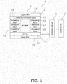
- Fig. 1 is a schematic diagram illustrating a structure of the pressure sensor according to the present invention. Note that the cross-sectional view of Fig. 1 is simply illustrates a schematic positional relationship among layers and does not accurately reproduce a real structure.
- the sensor device 1 is a device for detecting a pressing force.
- the sensor device 1 includes the pressure sensor 3.
- the pressure sensor 3 is a sensor that detects a change in a resistance when receiving a pressing force.
- the pressure sensor 3 mainly includes an upper layer 9, a lower layer 11, and an intermediate adhesion layer 13.
- the upper layer 9 includes an upper film 15 (one example of a first insulating base material) and a pressure-sensitive layer 17 (one example of a pressure-sensitive conductor).
- the upper film 15 is a layer to which a pressing force is applied from a human finger, for example.
- the pressure-sensitive layer 17 is formed on a lower surface of the upper film 15 (i.e. a surface on a lower film 19 side).
- the pressure-sensitive layer 17 is formed on the entire lower surface of the upper film 15. Expression "formed on the entire lower surface” means being formed solidly on the entire part necessary for contacting with electrodes described later.
- the lower layer 11 includes the lower film 19 (one example of a second insulating base material) and a wiring 21.
- the lower film 19 is disposed with a space interposed between itself and the upper film 15.
- the wiring 21 is formed on an upper surface of the lower film 19 (i.e. a surface on the upper film 15 side).
- An air layer 29 is secured between the wiring 21 and the pressure-sensitive layer 17.
- the intermediate adhesion layer 13 is a frame part between the upper layer 9 and the lower layer 11, which secures the air layer 29 described above.
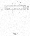
- the intermediate adhesion layer 13 includes an insulating layer 23, an insulating layer 25, and an adhesion layer 27.
- the insulating layer 23 is formed on the lower surface of the upper layer 9.
- the insulating layer 25 is formed on the upper surface of the lower layer 11.
- the adhesion layer 27 is disposed between the insulating layer 23 and the insulating layer 25 so as to adhere them. In this way, the upper layer 9 and the lower layer 11 are fixed in an insulating state. Note that the insulating layer 23 may be eliminated.
- the pressure-sensitive layer and the wiring are formed on opposed films respectively so as to be opposed to each other, and therefore the pressure-sensitive layer and the wiring may be upside down.
- the sensor device 1 includes a detection circuit 5.
- the detection circuit 5 is a device for detecting a pressing force when the pressing force is applied so that the pressure-sensitive layer 17 contacts with the wiring 21, by measuring a resistance in the wiring 21 and further by signal processing.
- the sensor device 1 includes a control unit 7.
- the control unit 7 is a device for controlling the detection circuit 5, transmitting an output from the detection circuit 5 to other device, and controlling a display unit for display.
- the control unit 7 is a computer including a CPU, a RAM, and a ROM.
- Fig. 2 is a side view of the pressure sensor.
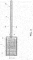
- Fig. 3 is a plan view of the pressure sensor.
- Fig. 4 is a II-II cross-sectional view of Fig. 3 .
- the lower film 19 includes an extension part 30 that further extends from a part opposed to the upper film 15.
- the extension part 30 includes a first wiring section 35 and a second wiring section 45 (described later).
- sensor output of the pressure sensor 3 is a one-side take-out type.
- the wiring 21 is constituted of a pair of electrode patterns having a comb-tooth shape (described later).
- the upper film 15 and the lower film 19 there is a material that can be used as a flexible substrate, for example, general-purpose resin such as polyethylene terephthalate, polystyrene resin, polyolefin resin, ABS resin, AS resin, acrylic resin, or AN resin.
- general-purpose resin such as polyethylene terephthalate, polystyrene resin, polyolefin resin, ABS resin, AS resin, acrylic resin, or AN resin.
- polystyrene resin polycarbonate resin, polyacetal resin, polycarbonate modified polyphenylene ether resin, polybutylene terephthalate resin, or ultra-high molecular weight polyethylene resin
- super engineering resin such as polysulfone resin, polyphenylene sulfide resin, polyphenylene oxide resin, polyallylate resin, polyetherimide resin, polyimide resin, liquid crystal polyester resin, or polyallyl heat resistant resin.
- the wiring 21 As a material of the wiring 21, there is a metal such as gold, silver, copper, or nickel, or paste made of carbon having electric conductivity. As a method of forming these, there is a printing method such as screen printing, offset printing, gravure printing, or flexographic printing, or a photoresist method. In addition, the wiring 21 can be formed also by adhering copper foil, gold foil, or other metal foil. Further, the wiring 21 can be formed also by forming an electrode pattern with resist on an FPC with plated metal such as copper and by etching a part of the metal foil that is not protected by the resist. Electrodes may be formed by a method described above or by combining or laminating materials.
- the wiring width is 30 to 500 ⁇ m, and the thickness is 1 to 100 ⁇ m.
- the material is copper
- the wiring width is 10 to 300 ⁇ m
- the thickness is 20 to 1000 nm.
- the pressure-sensitive layer 17 is made of a polymer containing, for example, carbon ink, PEDOT, or conductive particles.
- a composition of the pressure-sensitive layer 17 is constituted of a material whose electric characteristics such as a resistance value are changed in response to external force or the like.
- the pressure-sensitive layer 17 can be disposed on the lower film 19 by application.
- the insulating layers 23 and 25 are made of material such as polyol resin, isocyanate resin, methylene resin, acrylic resin, urethane resin, or silicone resin.
- the adhesion layer 27 is, for example, adhesive of acrylic resin, urethane resin or silicone resin.
- Fig. 5 is a schematic diagram illustrating a resistance measurement principle.
- the detection circuit 5 includes a DC power supply 22 and a resistance meter 24, which are connected in series, and ends of which are connected to a pair of electrode patterns of the wiring 21.
- the pair of electrodes conduct with each other via the pressure-sensitive layer 17 (details will be described later).
- the resistance meter 24 can measure the resistance. Note that when the pressing force increases, contact resistances between the pressure-sensitive layer 17 and the pair of electrodes are reduced. As a result, the magnitude of the pressing force can be accurately measured.
- Fig. 6 is a graph showing a change in a resistance R total with respect to a load (pressure-sensitive characteristics). It is understood from the curve indicated by a solid line that the resistance decreases as the load increases.
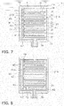
- FIGs. 7 and 8 are plan views illustrating an electrode pattern of the first example.
- the wiring includes a first electrode pattern 21A (one example of the first electrode pattern) and a second electrode pattern 21B (one example of the second electrode pattern).
- the first electrode pattern 21A includes a plurality of first electrode sections 31, a first interconnecting section 33, and a first wiring section 35.
- the plurality of first electrode sections 31 have a belt-like or strip-like shape extending in a left and right direction in the diagram, and are arranged with spaces in an up and down direction in the diagram.
- the first interconnecting section 33 extends in an up and down direction in the diagram and connects right side ends of the plurality of first electrode sections 31 in the diagram. Note that a lower end of the first interconnecting section 33 in the diagram is referred to as a first end 37, and an upper end in the diagram is referred to as a second end 39.
- the first wiring section 35 extends from the first end 37.
- the first wiring section 35 extends to the detection circuit 5 and has an output terminal that is connected to the detection circuit 5.
- the second electrode pattern 21B includes a plurality of second electrode sections 41, a second interconnecting section 43, and a second wiring section 45.
- the plurality of second electrode sections 41 have a belt-like or strip-like shape extending in the left and right direction in the diagram, and are arranged with spaces in an up and down direction in the diagram.
- the second electrode sections 41 and the first electrode sections 31 are alternately arranged.
- the second interconnecting section 43 extends in the up and down direction in the diagram and connects left side ends of the plurality of second electrode sections 41 in the diagram.
- a lower end of the second interconnecting section 43 in the diagram is referred to as a first end 47
- an upper end in the diagram is referred to as a second end 49.
- the first end 37 and the first end 47 are disposed on the same side
- the second end 39 and the second end 49 are disposed on the same side.
- the second end 49 is disposed at a diagonal position with respect to the first end 37.
- the second wiring section 45 extends from the second end 49. More specifically, the second wiring section 45 starts at the second end 49, extends along (i.e. passing close to) the second interconnecting section 43, further extends to approach the first wiring section 35, and finally extends in parallel to the first wiring section 35 in the vicinity of the first wiring section 35. In this way, the second wiring section 45 is longer than the first wiring section 35. Note that the second wiring section 45 extends to the detection circuit 5 and has an output terminal that is connected to the detection circuit 5.
- the first wiring section 35 extends from the first end 37 of the first interconnecting section 33, and the second wiring section 45 extends from the second end 49 of the second interconnecting section 43. Therefore, when the adjacent first electrode section 31 and second electrode section 41 contact with each other via the pressure-sensitive layer 17, resistance between the output terminal of the first wiring section 35 and the output terminal of the second wiring section 45 (the entire conduction path) is substantially equal in any combination of the first electrode section 31 and the second electrode section 41. This is further described in detail below.
- a first point P1 is pressed, and one of the first electrode sections 31 and one of the second electrode sections 41 conduct with each other via the pressure-sensitive layer 17 at a corresponding part.
- the first point P1 is positioned on an upper side in the diagram, i.e. on the side of the second end 39 and the second end 49.
- a conduction path A1 in the first electrode pattern 21A from the first point P1 includes the first electrode section 31, the first interconnecting section 33, and the first wiring section 35.
- a conduction path B1 in the second electrode pattern 21B from the first point P1 includes the second electrode section 41, the second interconnecting section 43, and the second wiring section 45.
- a conduction path A2 in the first electrode pattern 21A from the second point P2 includes the first electrode section 31, the first interconnecting section 33, and the first wiring section 35.
- a conduction path B2 in the second electrode pattern 21B from the second point P2 includes the second electrode section 41, the second interconnecting section 43, and the second wiring section 45.
- lengths of the entire conduction paths (A1+B1 and A2+B2) are substantially the same.
- variation of wiring resistance is equal to or less than 10% of a pressure-sensitive resistance value.
- the pressure-sensitive resistance value is a resistance value when a maximum load is applied in an implemented application.
- the second wiring section 45 extends from the first end 47 of the second interconnecting section 43 in the second electrode pattern 21B. Therefore, when the pressing force is applied so that the first electrode section 31 and the second electrode section 41 conduct with each other at a position close to the second end 39 and the second end 49 (in the first case), a conduction path in the first interconnecting section 33 (A1 in Fig. 7 ) and a conduction path in the second interconnecting section 43 (C1 in Fig. 7 ) are both long.
- the conduction path of the first interconnecting section 33 is still long, while the conduction path of the second interconnecting section 43 is shorter than that in the second case, and the resistance of the second wiring section 45 is added thereto.
- the entire conduction path is slightly higher than the conventional structure.
- the conduction path of the first interconnecting section 33 is still short, while the conduction path of the second interconnecting section 43 is long, and the resistance of the second wiring section 45 is added thereto.
- the entire conduction path is much more than the conventional structure.
- the resistance of the entire conduction path is substantially equal in any combination of the first electrode section 31 and the second electrode section 41. For example, almost the same resistance occurs as indicated in a solid line in Fig. 6 .
- FIGs. 9 and 10 are plan views illustrating an electrode pattern of the second example.
- the wiring includes a first electrode pattern 21C (one example of the first electrode pattern) and a second electrode pattern 21D (one example of the second electrode pattern).
- the first electrode pattern 21C includes the plurality of first electrode sections 31, the first interconnecting section 33, and a first wiring section 35A.
- the first electrode sections 31 have a belt-like or strip-like shape extending in the left and right direction in the diagram, and are arranged with spaces in an up and down direction in the diagram.
- the first interconnecting section 33 extends in the up and down direction in the diagram and connects left side ends of the plurality of first electrode sections 31 in the diagram.
- the first wiring section 35A extends from an end of the first interconnecting section 33. Note that a lower end of the first interconnecting section 33 in the diagram is referred to as a first end 37, while an upper end in the diagram is referred to as a second end 39.
- the first wiring section 35A extends from the first end 37.
- the first wiring section 35A extends to the detection circuit 5 and has an output terminal that is connected to the detection circuit 5.
- the second electrode pattern 21D includes a plurality of second electrode sections 41, a second interconnecting section 43, and a second wiring section 45A.
- the second electrode sections 41 have a belt-like or strip-like shape extending in the left and right direction in the diagram, and are arranged with spaces in the up and down direction in the diagram.
- the second electrode sections 41 and the first electrode sections 31 are alternately arranged.
- the second interconnecting section 43 extends in the up and down direction in the diagram and connects right side ends of the plurality of second electrode sections 41 in the diagram.
- a lower end of the second interconnecting section 43 in the diagram is referred to as a first end 47
- an upper end in the diagram is referred to as a second end 49.
- the first end 37 and the first end 47 are disposed on the same side
- the second end 39 and the second end 49 are disposed on the same side.
- the second end 49 is disposed at a diagonal position with respect to the first end 37.
- the second wiring section 45A extends from the second end 49. More specifically, the second wiring section 45A starts at the second end 49, extends along the first electrode section 31 disposed at the upper most position in the diagram, further extends along (i.e. passing close to) the first interconnecting section 33, and finally extends in parallel to the first wiring section 35A in a vicinity of the first wiring section 35A. In this way, the second wiring section 45A is longer than the first wiring section 35A. Note that the second wiring section 45A extends to the detection circuit 5 and has an output terminal that is connected to the detection circuit 5.
- the first wiring section 35A extends from the first end 37 of the first interconnecting section 33, and the second wiring section 45A extends from the second end 49 of the second interconnecting section 43. Therefore, when the adjacent first electrode section 31 and second electrode section 41 contact with each other via the pressure-sensitive layer 17, the resistance of the entire conduction path is substantially equal in any combination of the first electrode section 31 and the second electrode section 41. This is further described in detail below.
- the first point P1 is pressed, and one of the first electrode sections 31 and one of the second electrode sections 41 conduct with each other via the pressure-sensitive layer 17 at the corresponding part.
- the first point P1 is positioned on the upper side in the diagram, i.e. on the side of the second end 39 and the second end 49.
- a conduction path A3 in the first electrode pattern 21C from the first point P1 includes the first electrode section 31, the first interconnecting section 33, and the first wiring section 35A.
- a conduction path B3 in the second electrode pattern 21D from the first point P1 includes the second electrode section 41, the second interconnecting section 43, and the second wiring section 45A.
- a conduction path A4 in the first electrode pattern 21C from the second point P2 includes the first electrode section 31, the first interconnecting section 33, and the first wiring section 35A.
- a conduction path B4 in the second electrode pattern 21D from the second point P2 includes the second electrode section 41, the second interconnecting section 43, and the second wiring section 45A.
- FIGs. 11 to 12 are plan views illustrating an electrode pattern of the third example.
- the wiring includes a first electrode pattern 21E (one example of the first electrode pattern) and a second electrode pattern 21F (one example of the second electrode pattern).
- the first electrode pattern 21E includes a plurality of first electrode sections 31, a first interconnecting section 33, and a first wiring section 35B.
- the first electrode sections 31 have a belt-like or strip-like shape extending in the up and down direction in the diagram, and are arranged with spaces in the left and right direction in the diagram.
- the first interconnecting section 33 extends in the left and right direction in the diagram and connects lower ends of the plurality of first electrode sections 31 in the diagram. Note that the left side end of the first interconnecting section 33 in the diagram is referred to as a first end 37, while the right side end in the diagram is referred to as a second end 39.
- the first wiring section 35B extends from the first end 37.
- the first wiring section 35B extends to the detection circuit 5 and has an output terminal that is connected to the detection circuit 5.
- the second electrode pattern 21F includes a plurality of second electrode sections 41, a second interconnecting section 43, and a second wiring section 45B.
- the second electrode sections 41 have a belt-like or strip-like shape extending in the up and down direction in the diagram, and are arranged with spaces in the left and right direction in the diagram.
- the second electrode sections 41 and the first electrode sections 31 are alternately arranged.
- the second interconnecting section 43 extends in the left and right direction in the diagram and connects upper ends of the plurality of second electrode sections 41 in the diagram.
- the left side end of the second interconnecting section 43 in the diagram is referred to as a first end 47
- the right side end in the diagram is referred to as a second end 49.
- the first end 37 and the first end 47 are disposed on the same side
- the second end 39 and the second end 49 are disposed on the same side.
- the second end 49 is disposed at a diagonal position with respect to the first end 37.
- the second wiring section 45B extends from the second end 49. More specifically, the second wiring section 45B starts at the second end 49, extends along (i.e. passing close to) the second interconnecting section 43, further extends along the first electrode section 31 at the leftmost side in the diagram, and finally extends in parallel to the first wiring section 35B in a vicinity of the first wiring section 35B. In this way, the second wiring section 45B is longer than the first wiring section 35B. Note that the second wiring section 45B extends to the detection circuit 5 and has an output terminal that is connected to the detection circuit 5.
- the first wiring section 35B extends from the first end 37 of the first interconnecting section 33, and the second wiring section 45B extends from the second end 49 of the second interconnecting section 43. Therefore, when the adjacent first electrode section 31 and second electrode section 41 contact with each other via the pressure-sensitive layer 17, the resistance of the entire conduction path is substantially equal in any combination of the first electrode section 31 and the second electrode section 41.
- the first point P1 is pressed, and one of the first electrode sections 31 and one of the second electrode sections 41 conduct with each other via the pressure-sensitive layer 17 at the corresponding part.
- the first point P1 is positioned on the right side in the diagram, i.e. on the side of the second end 39 and the second end 49.
- a conduction path A5 in the first electrode pattern 21E from the first point P1 includes the first electrode section 31, the first interconnecting section 33, and the first wiring section 35B.
- a conduction path B5 in the second electrode pattern 21F from the first point P1 includes the second electrode section 41, the second interconnecting section 43, and the second wiring section 45B.
- a conduction path A6 in the first electrode pattern 21E from the second point P2 includes the first electrode section 31, the first interconnecting section 33, and the first wiring section 35B.
- a conduction path B6 in the second electrode pattern 21F from the second point P2 includes the second electrode section 41, the second interconnecting section 43, and the second wiring section 45B.
- FIGs. 13 and 14 are plan views illustrating an electrode pattern of the fourth example.
- two sets of wirings (a wiring 51 and a wiring 53) are disposed.
- the wirings 51 and 53 are formed at different positions on the same surface of the same film.
- the wiring 51 includes a first electrode pattern 21G (one example of the first electrode pattern) and a second electrode pattern 21H (one example of the second electrode pattern).
- the wiring 53 includes a first electrode pattern 21G (one example of the third electrode pattern) and a second electrode pattern 21H (one example of the fourth electrode pattern).
- the first electrode pattern 21G includes a plurality of first electrode sections 31, a first interconnecting section 33, and a first wiring section 35C.
- the first electrode sections 31 have a belt-like or strip-like shape extending in the left and right direction in the diagram, and are arranged with spaces in an up and down direction in the diagram.
- the first interconnecting section 33 extends in the up and down direction in the diagram and connects right side ends of the plurality of first electrode sections 31 in the diagram. Note that the lower end of the first interconnecting section 33 in the diagram is referred to as a first end 37, while the upper end in the diagram is referred to as a second end 39.
- the first wiring section 35C extends from the first end 37.
- the first wiring section 35C extends to the detection circuit 5 and has an output terminal that is connected to the detection circuit 5.
- the second electrode pattern 21H includes the plurality of second electrode sections 41, the second interconnecting section 43, and a second wiring section 45C.
- the second electrode sections 41 have a belt-like or strip-like shape extending in the left and right direction in the diagram, and are arranged with spaces in an up and down direction in the diagram.
- the second electrode sections 41 and the first electrode sections 31 are alternately arranged.
- the second interconnecting section 43 extends in the up and down direction in the diagram and connects the left side ends of the plurality of second electrode sections 41.
- the lower end of the second interconnecting section 43 in the diagram is referred to as a first end 47
- the upper end in the diagram is referred to as a second end 49.
- the first end 37 and the first end 47 are disposed on the same side
- the second end 39 and the second end 49 are disposed on the same side.
- the second end 49 is disposed at a diagonal position with respect to the first end 37.
- the second wiring section 45C extends from the second end 49. More specifically, the second wiring section 45C starts at the second end 49, extends along the first electrode section 31 on the uppermost side in Fig. 5 , further extends along (i.e. passing close to) the first interconnecting section 33, and finally extends in parallel to the first wiring section 35B in a vicinity of the first wiring section 35B. In this way, the second wiring section 45C is longer than the first wiring section 35C. Note that the second wiring section 45C extends to the detection circuit 5 and has an output terminal that is connected to the detection circuit 5.
- the first wiring section 35C extends from the first end 37 of the first interconnecting section 33, and the second wiring section 45C extends from the second end 49 of the second interconnecting section 43. Therefore, when the adjacent first electrode section 31 and second electrode section 41 contact with each other via the pressure-sensitive layer 17, the resistance of the entire conduction path is substantially equal in any combination of the first electrode section 31 and the second electrode section 41. This is further described in detail below.
- the first point P1 is pressed, and one of the first electrode sections 31 and one of the second electrode sections 41 conduct with each other via the pressure-sensitive layer 17 at the corresponding part.
- the first point P1 is positioned on the upper side in the diagram, i.e. on the side of the second end 39 and the second end 49.
- a conduction path A7 in the first electrode pattern 21G from the first point P1 includes the first electrode section 31, the first interconnecting section 33, and the first wiring section 35C.
- a conduction path B7 in the second electrode pattern 21H from the first point P1 includes the second electrode section 41, the second interconnecting section 43, and the second wiring section 45C.
- a conduction path A8 in the first electrode pattern 21G from the second point P2 includes the first electrode section 31, the first interconnecting section 33, and the first wiring section 35C.
- a conduction path B8 in the second electrode pattern 21H from the second point P2 includes the second electrode section 41, the second interconnecting section 43, and the second wiring section 45C.
- the wiring 53 has the same structure as the wiring 51 and has the same function.
- the four wiring sections extend to the detection circuit 5.
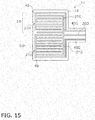
- Fig. 15 is a plan view illustrating an electrode pattern of the fifth example.
- a basic structure is the same as the fourth example.
- the difference is that the first wiring section 35C (one example of the first wiring section) of the first electrode pattern 21G of the wiring 51 (one example of the first electrode pattern) is common with the first wiring section 35C (one example of the third wiring section) of the first electrode pattern 21G of the wiring 53 (one example of the third electrode pattern).
- the number of the wiring sections can be reduced from four to three (i.e., one first wiring section 35D and two second wiring sections 45C), and thus material and an occupying area of the wiring sections can be reduced.
- the number of control signal wiring necessary on the IC side can be reduced.
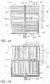
- FIG. 16 is a plan view illustrating an electrode pattern of the sixth example.
- a wiring 61, a wiring 63, a wiring 65, and a wiring 67 are disposed.
- the wiring 61, the wiring 63, the wiring 65, and the wiring 67 are formed at different positions on the same surface of the same film. Note that the wiring 61 and the wiring 65 are disposed on the side farther from the output terminal of the wiring section, while the wiring 63 and the wiring 67 are disposed on the side closer to the output terminal of the wiring section.
- the wiring 61 includes a first electrode pattern 211 (one example of the first electrode pattern) and a second electrode pattern 21J (one example of the second electrode pattern).
- the wiring 63 includes the first electrode pattern 211 (one example of the third electrode pattern) and the second electrode pattern 21J (one example of the fourth electrode pattern).
- the first electrode pattern 211 includes a plurality of first electrode sections 31, a first interconnecting section 33, and the first wiring section 35D.
- the plurality of first electrode sections 31 have a belt-like or strip-like shape extending in the left and right direction in the diagram, and are arranged with spaces in an up and down direction in the diagram.
- the first interconnecting section 33 extends in the up and down direction in the diagram and connects right side ends of the plurality of first electrode sections 31 in the diagram. Note that the lower end of the first interconnecting section 33 in the diagram is referred to as a first end 37, while the upper end in the diagram is referred to as a second end 39.
- the first wiring section 35D extends from the first end 37.
- the first wiring section 35D extends to the detection circuit 5 and has an output terminal that is connected to the detection circuit 5.
- the second electrode pattern 21J includes a plurality of second electrode sections 41, a second interconnecting section 43, and a second wiring section 45D.
- the plurality of second electrode sections 41 have a belt-like or strip-like shape extending in the left and right direction in the diagram, and are arranged with spaces in an up and down direction in the diagram.
- the second electrode sections 41 and the first electrode sections 31 are alternately arranged.
- the second interconnecting section 43 extends in the up and down direction in the diagram and connects the left side ends of the plurality of second electrode sections 41 in the diagram.
- a lower end of the second interconnecting section 43 in the diagram is referred to as a first end 47
- an upper end in the diagram is referred to as a second end 49.
- the first end 37 and the first end 47 are disposed on the same side
- the second end 39 and the second end 49 are disposed on the same side.
- the second end 49 is disposed at a diagonal position with respect to the first end 37.
- the second wiring section 45D extends from the second end 49. More specifically, the second wiring section 45D starts at the second end 49, extends along the first electrode section 31 on the uppermost side in the diagram, further extends along (i.e. passing close to) the first interconnecting section 33, and further extends along the first wiring section 35D. In this way, the second wiring section 45D is longer than the first wiring section 35D. Note that the second wiring section 45D extends to the detection circuit 5 and has an output terminal that is connected to the detection circuit 5.
- the first wiring section 35D extends from the first end 37 of the first interconnecting section 33, while the second wiring section 45D extends from the second end 49 of the second interconnecting section 43. Therefore, when the adjacent first electrode section 31 and second electrode section 41 contact with each other via the pressure-sensitive layer 17, resistance between the output terminal of the first wiring section 35D and the output terminal of the second wiring section 45D is substantially equal in any combination of the first electrode section 31 and the second electrode section 41.
- the wiring 63, the wiring 65, and the wiring 67 have the same structure as the wiring 61, and have the same function.
- the second wiring section 45D (one example of the second wiring section) of the second electrode pattern 21J of the wiring 61 (one example of the second electrode pattern) is common with the second wiring section 45D (one example of the fourth wiring section) of the second electrode pattern 21J of the wiring 63 (one example of the fourth electrode pattern).
- the second wiring section 45D of the wiring 65 is common with the second wiring section 45D of the wiring 67.
- the number of wiring sections disposed on the left and right frame areas is three each.
- FIG. 17 is a plan view illustrating an electrode pattern of the seventh example.
- a wiring 71, a wiring 73, a wiring 75, and a wiring 77 are disposed.
- the wiring 71, the wiring 73, the wiring 75, and the wiring 77 are formed at different positions on the same surface of the same film. Note that the wiring 71 and the wiring 75 are disposed on the side farther from the output terminal of the wiring section, while the wiring 73 and the wiring 77 are disposed on the side closer to the output terminal of the wiring section.
- the wiring 71 will be described.
- the wiring 71 includes a first electrode pattern 21K (one example of the first electrode pattern) and a second electrode pattern 21L (one example of the second electrode pattern).
- the wiring 73 includes the first electrode pattern 21K (one example of the third electrode pattern) and the second electrode pattern 21L (one example of the fourth electrode pattern).
- the first electrode pattern 21K includes a plurality of first electrode sections 31, a first interconnecting section 33, and a first wiring section 35E.
- the first electrode sections 31 have a belt-like or strip-like shape extending in the left and right direction in the diagram, and are arranged with spaces in an up and down direction in the diagram.
- the first interconnecting section 33 extends in the up and down direction in the diagram and connects the left side ends of the plurality of first electrode sections 31. Note that the lower end of the first interconnecting section 33 in the diagram is referred to as a first end 37, while the upper end in the diagram is referred to as a second end 39.
- the first wiring section 35E extends from the first end 37.
- the first wiring section 35E extends to the detection circuit 5 and has an output terminal that is connected to the detection circuit 5.
- the second electrode pattern 21L includes a plurality of second electrode sections 41, a second interconnecting section 43, and a second wiring section 45E.
- the second electrode sections 41 have a belt-like or strip-like shape extending in the left and right direction in the diagram, and are arranged with spaces in an up and down direction in the diagram.
- the second electrode sections 41 and the first electrode sections 31 are alternately arranged.
- the second interconnecting section 43 extends in the up and down direction in the diagram and connects right side ends of the plurality of second electrode sections 41 in the diagram.
- a lower end of the second interconnecting section 43 in the diagram is referred to as a first end 47
- an upper end in the diagram is referred to as a second end 49.
- the first end 37 and the first end 47 are disposed on the same side
- the second end 39 and the second end 49 are disposed on the same side.
- the second end 49 is disposed at a diagonal position with respect to the first end 37.
- the second wiring section 45E extends from the second end 49. More specifically, the second wiring section 45E starts at the second end 49, extends along (i.e. passing close to) the second interconnecting section 43, further extends along (i.e. passing close to) the second interconnecting section 43 of the wiring 73, and finally extends in parallel to the first wiring section 35E in a vicinity of the first wiring section 35E. In this way, the second wiring section 45E is longer than the first wiring section 35E. Note that the second wiring section 45E extends to the detection circuit 5 and has an output terminal that is connected to the detection circuit 5.
- the first wiring section 35E extends from the first end 37 of the first interconnecting section 33, while the second wiring section 45E extends from the second end 49 of the second interconnecting section 43. Therefore, when the adjacent first electrode section 31 and second electrode section 41 contact with each other via the pressure-sensitive layer 17, the resistance of the entire conduction path is substantially equal in any combination of the first electrode section 31 and the second electrode section 41.
- the wiring 73, the wiring 75, and the wiring 77 have the same structure as the wiring 71, and have the same function.
- the first wiring section 35E (one example of the first wiring section) of the first electrode pattern 21K of the wiring 71 (one example of the first electrode pattern) is common with the first wiring section 35E (one example of the third wiring section) of the first electrode pattern 21K of the wiring 73 (one example of the third electrode pattern), the first wiring section 35E of the first electrode pattern 21K of the wiring 75, and the first wiring section 35E of the first electrode pattern 21K of the wiring 77.
- originally eight wiring sections are reduced to five wiring sections (i.e., one first wiring section 35E and four second wiring sections 45E).
- the number of wiring sections disposed on the left and right frame areas is four each.
- FIG. 18 is a plan view illustrating an electrode pattern of the eighth example.
- a wiring 81, a wiring 83, a wiring 85, and a wiring 87 are disposed.
- the wiring 81, the wiring 83, the wiring 85, and the wiring 87 are formed at different positions on the same surface of the same film. Note that the wiring 81 and the wiring 85 are disposed on the side farther from the output terminal of the wiring section, while the wiring 83 and the wiring 87 are disposed on the side closer to the output terminal of the wiring section.
- the wiring 81 and the wiring 83 are described.
- the wiring 81 includes a first electrode pattern 21M (one example of the first electrode pattern) and a second electrode pattern 21N (one example of the second electrode pattern).
- the wiring 83 includes the first electrode pattern 21M (one example of the third electrode pattern) and the second electrode pattern 21N (one example of the fourth electrode pattern).
- the wiring 81 will be described in detail below.
- the first electrode pattern 21M includes a plurality of first electrode sections 31, a first interconnecting section 33, and a first wiring section 35F.
- the plurality of first electrode sections 31 have a belt-like or strip-like shape extending in the left and right direction in the diagram, and are arranged with spaces in an up and down direction in the diagram.
- the first interconnecting section 33 extends in the up and down direction in the diagram and connects right side ends of the plurality of first electrode sections 31 in the diagram. Note that the lower end of the first interconnecting section 33 in the diagram is referred to as a first end 37, while the upper end in the diagram is referred to as a second end 39.
- the first wiring section 35F extends from the first end 37. Specifically, the first wiring section 35F extends to pass on the right side in the diagram of the first wiring section 35F of the second wiring 83. The first wiring section 35F extends to the detection circuit 5 and has an output terminal that is connected to the detection circuit 5.
- the second electrode pattern 21N includes a plurality of second electrode sections 41, a second interconnecting section 43, and a second wiring section 45F.
- the plurality of second electrode sections 41 have a belt-like or strip-like shape extending in the left and right direction in the diagram, and are arranged with spaces in an up and down direction in the diagram.
- the second electrode sections 41 and the first electrode sections 31 are alternately arranged.
- the second interconnecting section 43 extends in the up and down direction in the diagram and connects the left side ends of the plurality of second electrode sections 41 in the diagram.
- the lower end of the second interconnecting section 43 in the diagram is referred to as a first end 47
- the upper end in the diagram is referred to as a second end 49.
- the first end 37 and the first end 47 are disposed on the same side
- the second end 39 and the second end 49 are disposed on the same side.
- the second end 49 is disposed at a diagonal position with respect to the first end 37.
- the second wiring section 45F extends from the second end 49. More specifically, the second wiring section 45F starts at the second end 49, extends upward in the diagram to be folded, extends along (i.e. passing close to) the second interconnecting section 43, further extends along (i.e. passing close to) the second interconnecting section 43 of the wiring 83, and finally extends in parallel to the first wiring section 35F in a vicinity of the first wiring section 35F. In this way, the second wiring section 45F is longer than the first wiring section 35F. Note that the second wiring section 45F extends to the detection circuit 5 and has an output terminal that is connected to the detection circuit 5.
- the second wiring section 45F extends between the wiring 81 and the wiring 85 and further between the wiring 83 and the wiring 87, so as to extend long at a position adjacent to each second interconnecting section 43.
- the first wiring section 35F extends from the first end 37 of the first interconnecting section 33, and the second wiring section 45F extends from the second end 49 of the second interconnecting section 43. Therefore, when the adjacent first electrode section 31 and second electrode section 41 conduct with each other via the pressure-sensitive layer 17, the resistance of the entire conduction path is substantially equal in any combination of the first electrode section 31 and the second electrode section 41.
- the wiring 83, the wiring 85, and the wiring 87 have the same structure as the wiring 81, and have the same function.
- the second wiring section 45F (one example of the second wiring section) of the second electrode pattern 21N of the wiring 81 (one example of the second electrode pattern) is common with the second wiring section 45F (one example of the fourth wiring section) of the second electrode pattern 21N of the wiring 83 (one example of the fourth electrode pattern), the second wiring section 45F of the second electrode pattern 21N of the wiring 85, and the second wiring section 45F of the second electrode pattern 21N of the wiring 87.
- originally eight wiring sections are reduced to five wiring sections (i.e., four first wiring sections 35F and one second wiring section 45F).
- the number of wiring sections disposed on the left and right frame areas is two each.
- FIG. 19 is a plan view illustrating an electrode pattern of the ninth example.
- a wiring 91, a wiring 93, a wiring 95, and a wiring 97 are disposed.
- the wiring 91, the wiring 93, the wiring 95, and the wiring 97 are formed at different positions on the same surface of the same film. Note that the wiring 91 and the wiring 95 are disposed on the side farther from the output terminal of the wiring section, while the wiring 93 and the wiring 97 are disposed on the side closer to the output terminal of the wiring section.
- the wiring 91 and the wiring 93 are described.
- the wiring 91 includes a first electrode pattern 210 (one example of the first electrode pattern) and a second electrode pattern 21P (one example of the second electrode pattern).
- the wiring 93 includes the first electrode pattern 210 (one example of the third electrode pattern) and the second electrode pattern 21P (one example of the fourth electrode pattern).
- the wiring 91 will be described in detail below.
- the first electrode pattern 210 includes a plurality of first electrode sections 31, a first interconnecting section 33, and a first wiring section 35G.
- the plurality of first electrode sections 31 have a belt-like or strip-like shape extending in the up and down direction in the diagram, and are arranged with spaces in the left and right direction in the diagram.
- the first interconnecting section 33 extends in the left and right direction in the diagram and connects lower ends of the plurality of first electrode sections 31 in the diagram. Note that the left side end of the first interconnecting section 33 in the diagram is referred to as a first end 37, while the right side end in the diagram is referred to as a second end 39.
- the first wiring section 35G extends from the first end 37. Specifically, the first wiring section 35G is disposed along (i.e. passing close to) the left side in the diagram of the third wiring 93. The first wiring section 35G extends to the detection circuit 5 and has an output terminal that is connected to the detection circuit 5.
- the second electrode pattern 21P includes a plurality of second electrode sections 41, a second interconnecting section 43, and a second wiring section 45G.
- the plurality of second electrode sections 41 have a belt-like or strip-like shape extending in the up and down direction in the diagram, and are arranged with spaces in the left and right direction in the diagram.
- the second electrode sections 41 and the first electrode sections 31 are alternately arranged.
- the second interconnecting section 43 extends in the left and right direction in the diagram and connects upper ends of the plurality of second electrode sections 41 in the diagram.
- the left side end of the second interconnecting section 43 in the diagram is referred to as a first end 47
- the right side end in the diagram is referred to as a second end 49.
- the first end 37 and the first end 47 are disposed on the same side
- the second end 39 and the second end 49 are disposed on the same side.
- the second end 49 is disposed at a diagonal position with respect to the first end 37.
- the second wiring section 45G extends from the second end 49. More specifically, the second wiring section 45G starts at the second end 49, extends along (i.e. passing close to) the first electrode section 31 on the rightmost side in the diagram, further extends along (i.e. passing close to) the second wiring section 45G of the wiring 93, and finally extends in parallel to the first wiring section 35G in a vicinity of the first wiring section 35G. In this way, the second wiring section 45G is longer than the first wiring section 35G. Note that the second wiring section 45G extends to the detection circuit 5 and has an output terminal that is connected to the detection circuit 5.
- the first wiring section 35G extends from the first end 37 of the first interconnecting section 33, and the second wiring section 45G extends from the second end 49 of the second interconnecting section 43. Therefore, when the adjacent first electrode section 31 and second electrode section 41 contact with each other via the pressure-sensitive layer 17, the resistance of the entire conduction path is substantially equal in any combination of the first electrode section 31 and the second electrode section 41.
- the wiring 93, the wiring 95, and the wiring 97 have the same structure as the wiring 91, and have the same function.
- the first wiring section 35G (one example of the first wiring section) of the first electrode pattern 210 of the wiring 91 (one example of the first electrode pattern) is common with the first wiring section 35G (one example of the third wiring section) of the first electrode pattern 210 of the wiring 93 (one example of the third electrode pattern), the first wiring section 35G of the first electrode pattern 210 of the wiring 95, and the first wiring section 35G of the first electrode pattern 210 of the wiring 97.
- originally eight wiring sections are reduced to five wiring sections (i.e., one first wiring section 35G and four second wiring sections 45G).
- the second wiring section 45G of the wiring 93 has the shape folded a plurality of times so that the length is increased.
- the number of wiring sections disposed on the left and right frame areas is two each.
- FIG. 20 is a plan view illustrating an electrode pattern of the tenth example.
- a wiring 201, a wiring 203, a wiring 205, and a wiring 207 are disposed.
- the wiring 201, the wiring 203, the wiring 205, and the wiring 207 are formed at different positions on the same surface of the same film. Note that the wiring 201 and the wiring 205 are disposed on the side farther from the output terminal of the wiring section, while the wiring 203 and the wiring 207 are disposed on the side closer to the output terminal of the wiring section.
- the wiring 201 and the wiring 203 are described.
- the wiring 201 includes a first electrode pattern 21Q (one example of the first electrode pattern) and a second electrode pattern 21R (one example of the second electrode pattern).
- the wiring 203 includes the first electrode pattern 21Q (one example of the third electrode pattern) and the second electrode pattern 21R (one example of the fourth electrode pattern).
- the wiring 201 will be described in detail below.
- the first electrode pattern 21Q includes a plurality of first electrode sections 31, a first interconnecting section 33, and a first wiring section 35H.
- the plurality of first electrode sections 31 have a belt-like or strip-like shape extending in the up and down direction in the diagram, and are arranged with spaces in the left and right direction in the diagram.
- the first interconnecting section 33 extends in the left and right direction in the diagram and connects lower ends of the plurality of first electrode sections 31 in the diagram. Note that the left side end of the first interconnecting section 33 in the diagram is referred to as a first end 37, while the right side end in the diagram is referred to as a second end 39.
- the first wiring section 35H extends from the first end 37.
- the first wiring section 35H extends to the detection circuit 5 and has an output terminal that is connected to the detection circuit 5.
- the second electrode pattern 21R includes a plurality of second electrode sections 41, a second interconnecting section 43, and a second wiring section 45H.
- the plurality of second electrode sections 41 have a belt-like or strip-like shape extending in the up and down direction in the diagram, and are arranged with spaces in the left and right direction in the diagram.
- the second electrode sections 41 and the first electrode sections 31 are alternately arranged.
- the second interconnecting section 43 extends in the left and right direction in the diagram and connects upper ends of the plurality of second electrode sections 41 in the diagram.
- the left side end of the second interconnecting section 43 in the diagram is referred to as a first end 47
- the right side end in the diagram is referred to as a second end 49.
- the first end 37 and the first end 47 are disposed on the same side
- the second end 39 and the second end 49 are disposed on the same side.
- the second end 49 is disposed at a diagonal position with respect to the first end 37.
- the second wiring section 45H extends from the second end 49. More specifically, the second wiring section 45H starts at the second end 49, extends along (i.e. passing close to) the first electrode section 31 on the rightmost side in the diagram, further extends along (i.e. passing close to) the first electrode section 31 on the rightmost side in the diagram of the wiring 203, and finally extends in parallel to the first wiring section 35H in a vicinity of the first wiring section 35H. In this way, the second wiring section 45H is longer than the first wiring section 35H. Note that the second wiring section 45H extends to the detection circuit 5 and has an output terminal that is connected to the detection circuit 5.
- the first wiring 201 and the second wiring 203 are line-symmetric, and the first interconnecting section 33 is common.
- the third wiring 205 and the fourth wiring 207 are line-symmetric, and the first interconnecting section 33 is common.
- the first wiring section 35H extends from the first end 37 of the first interconnecting section 33, and the second wiring section 45H extends from the second end 49 of the second interconnecting section 43. Therefore, when the adjacent first electrode section 31 and second electrode section 41 contact with each other via the pressure-sensitive layer 17, the resistance of the entire conduction path is substantially equal in any combination of the first electrode section 31 and the second electrode section 41.
- the wiring 203, the wiring 205, and the wiring 207 have the same structure as the wiring 201, and have the same function.
- the first wiring section 35H (one example of the first wiring section) of the first electrode pattern 21Q of the wiring 201 (one example of the first electrode pattern) is common with the first wiring section 35H (one example of the third wiring section) of the first electrode pattern 21Q of the wiring 203 (one example of the third electrode pattern), the first wiring section 35H of the first electrode pattern 21Q of the wiring 205, and the first wiring section 35H of the first electrode pattern 21Q of the wiring 207.
- originally eight wiring sections are reduced to five wiring sections (i.e., one first wiring section 35H and four second wiring sections 45H).
- the second wiring section 45H of the wiring 203 has the shape folded a plurality of times so that the length is increased.
- the number of wiring sections disposed on the left and right frame areas is one each.
- FIG. 21 is a schematic cross-sectional view of a display device to which the pressure sensor is applied.
- a display device 101 has a case 103.
- the case 103 has an upward open shape in the diagram.
- the display device 101 includes a glass 105.
- the lower surface of the glass 105 is fixed to the upper surface of a frame section of the case 103 with an adhesion layer 107.
- a space is secured between the glass 105 and the case 103.
- the display device 101 includes an LCD module 109.
- the LCD module 109 is disposed on the lower surface of the glass 105.
- the display device 101 includes a pressure sensor 111.
- the pressure sensor 111 is the same as the pressure sensor 3 described above.
- the display device 101 includes a cushioning material 113.
- the cushioning material 113 is disposed between the pressure sensor 111 and the bottom surface of the case 103.
- the cushioning material 113 is constituted of an elastically deformable material.
- the cushioning material 113 may be disposed only on the upper side of the pressure sensor 111, or both on the upper and lower sides of the pressure sensor 111.
- the pressing force acts on the pressure sensor 111 via the LCD module 109.
- the pressure sensor 111 detects the pressing force.
- an OLED may be used instead of the LCD module.
- the electrode pattern has a uniform line width, but the present invention is not limited to this as a matter of course.
- the space between the electrode sections is uniform, but the present invention is not limited to this as a matter of course.
- the electrode section has a linear shape, but the present invention is not limited to this as a matter of course.
- the present invention can be widely applied to pressure sensors in which a pressure-sensitive layer and a pair of electrode patterns are disposed to face each other with a space interposed therebetween.
Landscapes
- Engineering & Computer Science (AREA)
- Physics & Mathematics (AREA)
- General Physics & Mathematics (AREA)
- General Engineering & Computer Science (AREA)
- Theoretical Computer Science (AREA)
- Human Computer Interaction (AREA)
- Force Measurement Appropriate To Specific Purposes (AREA)
- Push-Button Switches (AREA)
Abstract
Description
- The present invention relates to a pressure sensor, particularly to a pressure sensor in which a pressure-sensitive layer faces a pair of electrode patterns with a space interposed therebetween.
- Conventionally, as a sensor having a pressing detection function for detecting a pressing force, a pressure sensor is known (for example, see Patent Citation 1).
- A pressure sensor 1 described in Patent Citation 1 includes a pressure-sensitive
thin film 3, andelectrode sections 41 and 42, which face each other with a space interposed therebetween. Theelectrode sections 41 and 42 illustrated inFig. 11 have a comb-tooth shape. When a pressing force is applied, a pair of comb teeth of theelectrode sections 41 and 42 are connected via the pressure-sensitivethin film 3. In this way, based on resistance values of theelectrode sections 41 and 42 and the pressure-sensitivethin film 3 at the contact position, a pressure detection unit detects the pressing force. - Patent Citation 1:
JP-A-2012-247372 - A pressure-sensitive resistance of a conduction path (between output terminals of the electrodes) of the pressure sensor 1 described above is the sum of a first electrode wiring resistance, a contact resistance between the first electrode and the pressure-sensitive thin film, a resistance of the pressure-sensitive thin film, a contact resistance between a second electrode and the pressure-sensitive thin film, and a second electrode wiring resistance. Depending on the magnitude of the pressing force, the contact resistance is varied. In this way, the pressing force is measured.
- Note that, if the pressing position is different, a conduction path length of the electrode wiring may be largely different regardless of the magnitude of the pressing force. Therefore, even the same pressing force may cause different resistance of the entire conduction path depending on the pressing position. However, in a case of a pressure sensor as a substitution of a general membrane switch, the contact resistance is sufficiently larger than a conduction path resistance of the electrode wiring, and hence a variation in the conduction path resistance of the electrode wiring can be ignored without a problem.
- On the other hand, in an upsized pressure sensor, a ratio of the conduction path resistance of the electrode wiring becomes large, and because of this difference, a detection value of the resistance corresponding to the pressing force may be largely changed.
- It is an object of the present invention to eliminate an in-surface sensitive variation of the pressing force in the pressure sensor.
- Aspects of the present invention are explained below as the technical solution. These aspects can be arbitrarily combined as needed.
- A pressure sensor according to one aspect of the present invention comprises a first insulating base material, a second insulating base material, a pressure-sensitive conductor, a first electrode pattern, and a second electrode pattern, a first wiring section, and a second wiring section.
- The second insulating base material is disposed with a space interposed between itself and the first insulating base material.
- The pressure-sensitive conductor is formed on an entire surface of the first insulating base material on the second insulating base material side.
- The first electrode pattern is formed on a surface of the second insulating base material on the first insulating base material side. The first electrode pattern includes a plurality of first electrodes, a first interconnecting section having a first end and extending to connect first end portions of the plurality of first electrodes, and a first wiring section extending from the first end of the first interconnecting section.
- The second electrode pattern is formed on a surface of the second insulating base material on the first insulating base material side. The second electrode pattern includes a plurality of second electrodes arranged alternately with the first electrodes, a second interconnecting section extending to connect first end portions of the plurality of second electrodes and having a second end disposed at a diagonal position with respect to the first end, and a second wiring section extending from the second end of the second interconnecting section.
- The second wiring section extends so that a conduction path resistance between an output terminal of the first wiring section and an output terminal of the second wiring section is substantially equal in any combination of the first electrode and the second electrode, when adjacent first electrode and second electrode conduct with each other via the pressure-sensitive conductor.
- It should be noted that "extending from the end" means that it extends from anywhere having a length at or near the end (the same interpretation will be employed below.).
- According to the sensor, the first wiring section extends from the first end of the first connecting portion, and the second wiring section extends the second end of the second connecting portion. Accordingly, the total resistance of the resistance of the first wiring section and the resistance of the second wiring section is substantially equal in any combination of the first electrode section and the second electrode section when the first electrode and the second electrode conduct with each other via the pressure conductive member.
- In a conventional structure, the second wiring section extends from the first end of the second interconnecting section in the second electrode pattern. Therefore, when the pressing force is applied so that the first electrode section and the second electrode section conduct with each other at a position close to the second end (in the first case), a conduction path in the first interconnecting section and a conduction path in the second interconnecting section are both long. In contrast, when the pressing force is applied so that the first electrode section and the second electrode section conduct with each other at a position close to the first end (in the second case), a conduction path in the first interconnecting section and a conduction path in the second interconnecting section are both short. Thus, the entire conduction path length in the interconnecting section is different between the first case and the second case, and hence resistance of the entire conduction path is largely different depending on a combination of the first electrode and the second electrode.
- In contrast, according to the present invention, in the first case, the conduction path of the first interconnecting section is still long, while the conduction path of the second interconnecting section is shorter than that in the second case, and the resistance of the second wiring section is added thereto. As a result, the entire conduction path is slightly higher than the conventional structure. In the second case, the conduction path of the first interconnecting section is still short, while the conduction path of the second interconnecting section becomes long, and the resistance of the second wiring section is added thereto. As a result, the entire conduction path is much more than the conventional structure. Further, as a result, the resistance of the entire conduction path is substantially equal in any combination of the first electrode and the second electrode.
- A variation in the conduction path resistance between the output terminal of the first wiring section and the output terminal of the second wiring section may be equal to or less than 10% of a pressure-sensitive resistance when a maximum load is applied.
- The second wiring section may extend to pass close to the second interconnecting section.
- The second wiring section may extend to pass close to the first interconnecting section.
- A pressure sensor according to another aspect of the present invention comprises a first insulating base material, a second insulating base material, a pressure-sensitive conductor, a first electrode pattern, a second electrode pattern, a first wiring section, a second wiring section, a third electrode pattern, a fourth electrode pattern, a third wiring section, and a fourth wiring section.
- The second insulating base material is disposed with a space interposed between itself and the first insulating base material.
- The pressure-sensitive conductor is formed on an entire surface of the first insulating base material on the second insulating base material side.
- The first electrode pattern is formed on a surface of the second insulating base material on the first insulating base material side. The first electrode pattern includes a plurality of first electrodes, a first interconnecting section having a first end and extending to connect first end portions of the plurality of first electrodes, and a first wiring section extending from the first end of the first interconnecting section.
- The second electrode pattern is formed on a surface of the second insulating base material on the first insulating base material side. The second electrode pattern includes a plurality of second electrodes arranged alternately with the first electrodes, a second interconnecting section extending to connect first end portions of the plurality of second electrodes and having a second end disposed at a diagonal position with respect to the first end, and a second wiring section extending from the second end of the second interconnecting section.
- The second wiring section extends so that a conduction path resistance between an output terminal of the first wiring section and an output terminal of the second wiring section is substantially equal in any combination of the first electrode and the second electrode, when adjacent first electrode and second electrode conduct with each other via the pressure-sensitive conductor.
- The third electrode pattern is formed on a surface of the second insulating base material on the first insulating base material side. The third electrode pattern includes a plurality of third electrodes, a third interconnecting section having a third end and extending to connect first end portions of the plurality of third electrodes, and a third wiring section extending from a third end of the third interconnecting section;
- The fourth electrode pattern is formed on a surface of the second insulating base material on the first insulating base material side. The fourth electrode pattern includes a plurality of fourth electrodes arranged alternately with the third electrodes, a fourth interconnecting section extending to connect first end portions of the plurality of fourth electrodes and having a fourth end disposed at a diagonal position with respect to the third end, and a fourth wiring section extending from the fourth end of the fourth interconnecting section.
- The fourth wiring section extends so that a conduction path resistance between an output terminal of the third wiring section and an output terminal of the fourth wiring section is substantially equal in any combination of the third electrode and the fourth electrode, when adjacent third electrode and fourth electrode conduct with each other via the pressure-sensitive conductor.
- According to the sensor, a plurality of sensors are disposed at different positions over the plane. Accordingly, the pressing forces at different areas can be detected simultaneously.
- A variation in the conduction path resistance between the output terminal of the first wiring section and the output terminal of the second wiring section may be equal to or less than 10% of a pressure-sensitive resistance when a maximum load is applied. A variation in the conduction path resistance between the output terminal of the third end and the output terminal of the fourth end may be equal to or less than 10% of a pressure-sensitive resistance when a maximum load is applied.
- The first wiring section and the third wiring section maybe common, or the second wiring section and the fourth wiring section are common. In this case, the number and an occupying area of the wiring sections can be reduced. In particular, the number of control signal wiring necessary on the IC side can be reduced.
- According to a pressure sensor of the present invention, the resistance of the conduction path between the output terminal of the first wiring section the output terminal of the second wiring section is substantially equal in any combination of the first electrode and the second electrode.
-
-
Fig. 1 is a schematic diagram illustrating a structure of a pressure sensor according to the present invention. -
Fig. 2 is a side view of the pressure sensor. -
Fig. 3 is a plan view of the pressure sensor. -
Fig. 4 is a II-II cross-sectional view ofFig. 3 . -
Fig. 5 is a schematic diagram illustrating a principle of resistance measurement. -
Fig. 6 is a graph showing a change in a resistance Rtotal with respect to a load (pressure-sensitive characteristics). -
Fig. 7 is a plan view illustrating an electrode pattern of a first example. -
Fig. 8 is a plan view illustrating the electrode pattern of the first example. -
Fig. 9 is a plan view illustrating an electrode pattern of a second example. -
Fig. 10 is a plan view illustrating the electrode pattern of the second example. -
Fig. 11 is a plan view illustrating an electrode pattern of a third example. -
Fig. 12 is a plan view illustrating the electrode pattern of the third example. -
Fig. 13 is a plan view illustrating an electrode pattern of a fourth example. -
Fig. 14 is a plan view illustrating the electrode pattern of the fourth example. -
Fig. 15 is a plan view illustrating an electrode pattern of a fifth example. -
Fig. 16 is a plan view illustrating an electrode pattern of a sixth example. -
Fig. 17 is a plan view illustrating an electrode pattern of a seventh example. -
Fig. 18 is a plan view illustrating an electrode pattern of an eighth example. -
Fig. 19 is a plan view illustrating an electrode pattern of a ninth example. -
Fig. 20 is a plan view illustrating an electrode pattern of a tenth example. -
Fig. 21 is a schematic cross-sectional view of a display device to which the pressure sensor is applied. - With reference to
Fig. 1 , a sensor device 1 including apressure sensor 3 will be described.Fig. 1 is a schematic diagram illustrating a structure of the pressure sensor according to the present invention. Note that the cross-sectional view ofFig. 1 is simply illustrates a schematic positional relationship among layers and does not accurately reproduce a real structure. - The sensor device 1 is a device for detecting a pressing force. The sensor device 1 includes the
pressure sensor 3. Thepressure sensor 3 is a sensor that detects a change in a resistance when receiving a pressing force. - The
pressure sensor 3 mainly includes anupper layer 9, alower layer 11, and anintermediate adhesion layer 13. - The
upper layer 9 includes an upper film 15 (one example of a first insulating base material) and a pressure-sensitive layer 17 (one example of a pressure-sensitive conductor). Theupper film 15 is a layer to which a pressing force is applied from a human finger, for example. The pressure-sensitive layer 17 is formed on a lower surface of the upper film 15 (i.e. a surface on alower film 19 side). The pressure-sensitive layer 17 is formed on the entire lower surface of theupper film 15. Expression "formed on the entire lower surface" means being formed solidly on the entire part necessary for contacting with electrodes described later. - The
lower layer 11 includes the lower film 19 (one example of a second insulating base material) and awiring 21. Thelower film 19 is disposed with a space interposed between itself and theupper film 15. Thewiring 21 is formed on an upper surface of the lower film 19 (i.e. a surface on theupper film 15 side). Anair layer 29 is secured between thewiring 21 and the pressure-sensitive layer 17. - The
intermediate adhesion layer 13 is a frame part between theupper layer 9 and thelower layer 11, which secures theair layer 29 described above. Theintermediate adhesion layer 13 includes an insulatinglayer 23, an insulatinglayer 25, and anadhesion layer 27. The insulatinglayer 23 is formed on the lower surface of theupper layer 9. The insulatinglayer 25 is formed on the upper surface of thelower layer 11. Theadhesion layer 27 is disposed between the insulatinglayer 23 and the insulatinglayer 25 so as to adhere them. In this way, theupper layer 9 and thelower layer 11 are fixed in an insulating state. Note that the insulatinglayer 23 may be eliminated. - In the example described above, it is sufficient if the pressure-sensitive layer and the wiring are formed on opposed films respectively so as to be opposed to each other, and therefore the pressure-sensitive layer and the wiring may be upside down.
- The sensor device 1 includes a
detection circuit 5. Thedetection circuit 5 is a device for detecting a pressing force when the pressing force is applied so that the pressure-sensitive layer 17 contacts with thewiring 21, by measuring a resistance in thewiring 21 and further by signal processing. - The sensor device 1 includes a
control unit 7. Thecontrol unit 7 is a device for controlling thedetection circuit 5, transmitting an output from thedetection circuit 5 to other device, and controlling a display unit for display. Thecontrol unit 7 is a computer including a CPU, a RAM, and a ROM. - With reference to
Figs. 2 to 4 , thepressure sensor 3 will be described in detail.Fig. 2 is a side view of the pressure sensor.Fig. 3 is a plan view of the pressure sensor.Fig. 4 is a II-II cross-sectional view ofFig. 3 . - As illustrated in
Figs. 2 and3 , thelower film 19 includes anextension part 30 that further extends from a part opposed to theupper film 15. Theextension part 30 includes afirst wiring section 35 and a second wiring section 45 (described later). As described above, sensor output of thepressure sensor 3 is a one-side take-out type. - Further, as illustrated in
Figs. 3 and4 , thewiring 21 is constituted of a pair of electrode patterns having a comb-tooth shape (described later). - As a material of the
upper film 15 and thelower film 19, there is a material that can be used as a flexible substrate, for example, general-purpose resin such as polyethylene terephthalate, polystyrene resin, polyolefin resin, ABS resin, AS resin, acrylic resin, or AN resin. In addition, it is also possible to use general-purpose engineering resin such as polystyrene resin, polycarbonate resin, polyacetal resin, polycarbonate modified polyphenylene ether resin, polybutylene terephthalate resin, or ultra-high molecular weight polyethylene resin, or super engineering resin such as polysulfone resin, polyphenylene sulfide resin, polyphenylene oxide resin, polyallylate resin, polyetherimide resin, polyimide resin, liquid crystal polyester resin, or polyallyl heat resistant resin. - As a material of the
wiring 21, there is a metal such as gold, silver, copper, or nickel, or paste made of carbon having electric conductivity. As a method of forming these, there is a printing method such as screen printing, offset printing, gravure printing, or flexographic printing, or a photoresist method. In addition, thewiring 21 can be formed also by adhering copper foil, gold foil, or other metal foil. Further, thewiring 21 can be formed also by forming an electrode pattern with resist on an FPC with plated metal such as copper and by etching a part of the metal foil that is not protected by the resist. Electrodes may be formed by a method described above or by combining or laminating materials. - As one example, when using screen printing, silver ink is the material, the wiring width is 30 to 500 µm, and the thickness is 1 to 100 µm. As another example, when using photolithography, the material is copper, the wiring width is 10 to 300 µm, and the thickness is 20 to 1000 nm.
- The pressure-
sensitive layer 17 is made of a polymer containing, for example, carbon ink, PEDOT, or conductive particles. A composition of the pressure-sensitive layer 17 is constituted of a material whose electric characteristics such as a resistance value are changed in response to external force or the like. The pressure-sensitive layer 17 can be disposed on thelower film 19 by application. As an application method of the pressure-sensitive layer 17, there is a printing method such as screen printing, offset printing, gravure printing, or flexographic printing. - The insulating layers 23 and 25 are made of material such as polyol resin, isocyanate resin, methylene resin, acrylic resin, urethane resin, or silicone resin. The
adhesion layer 27 is, for example, adhesive of acrylic resin, urethane resin or silicone resin. - With reference to
Fig. 5 , a resistance detection principle by thedetection circuit 5 will be described.Fig. 5 is a schematic diagram illustrating a resistance measurement principle. Thedetection circuit 5 includes aDC power supply 22 and aresistance meter 24, which are connected in series, and ends of which are connected to a pair of electrode patterns of thewiring 21. In this way, when the pressure-sensitive layer 17 contacts with a pair of electrodes by a pressing force as illustrated inFig. 5 , the pair of electrodes conduct with each other via the pressure-sensitive layer 17 (details will be described later). In this way, theresistance meter 24 can measure the resistance. Note that when the pressing force increases, contact resistances between the pressure-sensitive layer 17 and the pair of electrodes are reduced. As a result, the magnitude of the pressing force can be accurately measured. - With reference to
Fig. 6 , a change in the resistance corresponding to a load will be described.Fig. 6 is a graph showing a change in a resistance Rtotal with respect to a load (pressure-sensitive characteristics). It is understood from the curve indicated by a solid line that the resistance decreases as the load increases. - With reference to
Figs. 7 and 8 , a structure of a first example of the wiring will be described.Figs. 7 and 8 are plan views illustrating an electrode pattern of the first example. - The wiring includes a
first electrode pattern 21A (one example of the first electrode pattern) and asecond electrode pattern 21B (one example of the second electrode pattern). - The
first electrode pattern 21A includes a plurality offirst electrode sections 31, a first interconnectingsection 33, and afirst wiring section 35. The plurality offirst electrode sections 31 have a belt-like or strip-like shape extending in a left and right direction in the diagram, and are arranged with spaces in an up and down direction in the diagram. Thefirst interconnecting section 33 extends in an up and down direction in the diagram and connects right side ends of the plurality offirst electrode sections 31 in the diagram. Note that a lower end of the first interconnectingsection 33 in the diagram is referred to as afirst end 37, and an upper end in the diagram is referred to as asecond end 39. - The
first wiring section 35 extends from thefirst end 37. Thefirst wiring section 35 extends to thedetection circuit 5 and has an output terminal that is connected to thedetection circuit 5. - The
second electrode pattern 21B includes a plurality ofsecond electrode sections 41, asecond interconnecting section 43, and asecond wiring section 45. The plurality ofsecond electrode sections 41 have a belt-like or strip-like shape extending in the left and right direction in the diagram, and are arranged with spaces in an up and down direction in the diagram. Thesecond electrode sections 41 and thefirst electrode sections 31 are alternately arranged. Thesecond interconnecting section 43 extends in the up and down direction in the diagram and connects left side ends of the plurality ofsecond electrode sections 41 in the diagram. Note that a lower end of the second interconnectingsection 43 in the diagram is referred to as afirst end 47, and an upper end in the diagram is referred to as asecond end 49. In other words, thefirst end 37 and thefirst end 47 are disposed on the same side, while thesecond end 39 and thesecond end 49 are disposed on the same side. In other words, thesecond end 49 is disposed at a diagonal position with respect to thefirst end 37. - The
second wiring section 45 extends from thesecond end 49. More specifically, thesecond wiring section 45 starts at thesecond end 49, extends along (i.e. passing close to) the second interconnectingsection 43, further extends to approach thefirst wiring section 35, and finally extends in parallel to thefirst wiring section 35 in the vicinity of thefirst wiring section 35. In this way, thesecond wiring section 45 is longer than thefirst wiring section 35. Note that thesecond wiring section 45 extends to thedetection circuit 5 and has an output terminal that is connected to thedetection circuit 5. - In this
pressure sensor 3, thefirst wiring section 35 extends from thefirst end 37 of the first interconnectingsection 33, and thesecond wiring section 45 extends from thesecond end 49 of the second interconnectingsection 43. Therefore, when the adjacentfirst electrode section 31 andsecond electrode section 41 contact with each other via the pressure-sensitive layer 17, resistance between the output terminal of thefirst wiring section 35 and the output terminal of the second wiring section 45 (the entire conduction path) is substantially equal in any combination of thefirst electrode section 31 and thesecond electrode section 41. This is further described in detail below. - As illustrated in
Fig. 7 , a first point P1 is pressed, and one of thefirst electrode sections 31 and one of thesecond electrode sections 41 conduct with each other via the pressure-sensitive layer 17 at a corresponding part. As illustrated inFig. 7 , the first point P1 is positioned on an upper side in the diagram, i.e. on the side of thesecond end 39 and thesecond end 49. In this case, a conduction path A1 in thefirst electrode pattern 21A from the first point P1 includes thefirst electrode section 31, the first interconnectingsection 33, and thefirst wiring section 35. Further, a conduction path B1 in thesecond electrode pattern 21B from the first point P1 includes thesecond electrode section 41, the second interconnectingsection 43, and thesecond wiring section 45. - As illustrated in
Fig. 8 , when a second point P2 is pressed, one of thefirst electrode sections 31 and one of thesecond electrode sections 41 conduct with each other via the pressure-sensitive layer 17 at the corresponding part. As illustrated inFig. 8 , the second point P2 is positioned on a lower side in the diagram, i.e. on the side of thefirst end 37 and thefirst end 47. In this case, a conduction path A2 in thefirst electrode pattern 21A from the second point P2 includes thefirst electrode section 31, the first interconnectingsection 33, and thefirst wiring section 35. Further, a conduction path B2 in thesecond electrode pattern 21B from the second point P2 includes thesecond electrode section 41, the second interconnectingsection 43, and thesecond wiring section 45. - As described above, between cases of the first point P1 and the second point P2 are pressed, lengths of the entire conduction paths (A1+B1 and A2+B2) are substantially the same. Specifically, variation of wiring resistance is equal to or less than 10% of a pressure-sensitive resistance value. Note that the pressure-sensitive resistance value is a resistance value when a maximum load is applied in an implemented application.
- In a conventional structure, the
second wiring section 45 extends from thefirst end 47 of the second interconnectingsection 43 in thesecond electrode pattern 21B. Therefore, when the pressing force is applied so that thefirst electrode section 31 and thesecond electrode section 41 conduct with each other at a position close to thesecond end 39 and the second end 49 (in the first case), a conduction path in the first interconnecting section 33 (A1 inFig. 7 ) and a conduction path in the second interconnecting section 43 (C1 inFig. 7 ) are both long. In addition, in the conventional structure, when the pressing force is applied so that thefirst electrode section 31 and thesecond electrode section 41 conduct with each other at a position close to thefirst end 37 and the first end 47 (in the second case), a conduction path in the first interconnecting section 33 (A2 inFig. 8 ) and a conduction path in the second interconnecting section 43 (C2 inFig. 8 ) are both short. Thus, in the conventional structure, the entire conduction path length in the interconnecting section is different between the first case and the second case, and hence resistance of the entire conduction path is largely different depending on a combination of thefirst electrode section 31 and thesecond electrode section 41. As a result, for example, resistance difference ΔRAg is generated as indicated in broken lines inFig. 6 . - In this embodiment, in the first case, the conduction path of the first interconnecting
section 33 is still long, while the conduction path of the second interconnectingsection 43 is shorter than that in the second case, and the resistance of thesecond wiring section 45 is added thereto. As a result, the entire conduction path is slightly higher than the conventional structure. In the second case, the conduction path of the first interconnectingsection 33 is still short, while the conduction path of the second interconnectingsection 43 is long, and the resistance of thesecond wiring section 45 is added thereto. As a result, the entire conduction path is much more than the conventional structure. Further, as a result, the resistance of the entire conduction path is substantially equal in any combination of thefirst electrode section 31 and thesecond electrode section 41. For example, almost the same resistance occurs as indicated in a solid line inFig. 6 . - With reference to
Figs. 9 and 10 , a structure of a second example of the wiring will be described.Figs. 9 and 10 are plan views illustrating an electrode pattern of the second example. - The wiring includes a first electrode pattern 21C (one example of the first electrode pattern) and a
second electrode pattern 21D (one example of the second electrode pattern). - The first electrode pattern 21C includes the plurality of
first electrode sections 31, the first interconnectingsection 33, and afirst wiring section 35A. Thefirst electrode sections 31 have a belt-like or strip-like shape extending in the left and right direction in the diagram, and are arranged with spaces in an up and down direction in the diagram. Thefirst interconnecting section 33 extends in the up and down direction in the diagram and connects left side ends of the plurality offirst electrode sections 31 in the diagram. Thefirst wiring section 35A extends from an end of the first interconnectingsection 33. Note that a lower end of the first interconnectingsection 33 in the diagram is referred to as afirst end 37, while an upper end in the diagram is referred to as asecond end 39. - The
first wiring section 35A extends from thefirst end 37. Thefirst wiring section 35A extends to thedetection circuit 5 and has an output terminal that is connected to thedetection circuit 5. - The
second electrode pattern 21D includes a plurality ofsecond electrode sections 41, asecond interconnecting section 43, and asecond wiring section 45A. Thesecond electrode sections 41 have a belt-like or strip-like shape extending in the left and right direction in the diagram, and are arranged with spaces in the up and down direction in the diagram. Thesecond electrode sections 41 and thefirst electrode sections 31 are alternately arranged. Thesecond interconnecting section 43 extends in the up and down direction in the diagram and connects right side ends of the plurality ofsecond electrode sections 41 in the diagram. Note that a lower end of the second interconnectingsection 43 in the diagram is referred to as afirst end 47, and an upper end in the diagram is referred to as asecond end 49. In other words, thefirst end 37 and thefirst end 47 are disposed on the same side, while thesecond end 39 and thesecond end 49 are disposed on the same side. In other words, thesecond end 49 is disposed at a diagonal position with respect to thefirst end 37. - The
second wiring section 45A extends from thesecond end 49. More specifically, thesecond wiring section 45A starts at thesecond end 49, extends along thefirst electrode section 31 disposed at the upper most position in the diagram, further extends along (i.e. passing close to) the first interconnectingsection 33, and finally extends in parallel to thefirst wiring section 35A in a vicinity of thefirst wiring section 35A. In this way, thesecond wiring section 45A is longer than thefirst wiring section 35A. Note that thesecond wiring section 45A extends to thedetection circuit 5 and has an output terminal that is connected to thedetection circuit 5. - In this
pressure sensor 3, thefirst wiring section 35A extends from thefirst end 37 of the first interconnectingsection 33, and thesecond wiring section 45A extends from thesecond end 49 of the second interconnectingsection 43. Therefore, when the adjacentfirst electrode section 31 andsecond electrode section 41 contact with each other via the pressure-sensitive layer 17, the resistance of the entire conduction path is substantially equal in any combination of thefirst electrode section 31 and thesecond electrode section 41. This is further described in detail below. - As illustrated in
Fig. 9 , the first point P1 is pressed, and one of thefirst electrode sections 31 and one of thesecond electrode sections 41 conduct with each other via the pressure-sensitive layer 17 at the corresponding part. As illustrated inFig. 9 , the first point P1 is positioned on the upper side in the diagram, i.e. on the side of thesecond end 39 and thesecond end 49. In this case, a conduction path A3 in the first electrode pattern 21C from the first point P1 includes thefirst electrode section 31, the first interconnectingsection 33, and thefirst wiring section 35A. Further, a conduction path B3 in thesecond electrode pattern 21D from the first point P1 includes thesecond electrode section 41, the second interconnectingsection 43, and thesecond wiring section 45A. - As illustrated in
Fig. 10 , when the second point P2 is pressed, one of thefirst electrode sections 31 and one of thesecond electrode sections 41 conduct with each other via the pressure-sensitive layer 17 at the corresponding part. As illustrated inFig. 10 , the second point P2 is positioned on a lower side in the diagram, i.e. on the side of thefirst end 37 and thefirst end 47. In this case, a conduction path A4 in the first electrode pattern 21C from the second point P2 includes thefirst electrode section 31, the first interconnectingsection 33, and thefirst wiring section 35A. Further, a conduction path B4 in thesecond electrode pattern 21D from the second point P2 includes thesecond electrode section 41, the second interconnectingsection 43, and thesecond wiring section 45A. - As described above, between cases of the first point P1 and the second point P2 are pressed, lengths of the entire conduction paths (A3+B3 and A4+B4) are substantially the same.
- With reference to
Figs. 11 to 12 , a structure of a third example of the wiring will be described.Figs. 11 to 12 are plan views illustrating an electrode pattern of the third example. - The wiring includes a
first electrode pattern 21E (one example of the first electrode pattern) and asecond electrode pattern 21F (one example of the second electrode pattern). - The
first electrode pattern 21E includes a plurality offirst electrode sections 31, a first interconnectingsection 33, and afirst wiring section 35B. Thefirst electrode sections 31 have a belt-like or strip-like shape extending in the up and down direction in the diagram, and are arranged with spaces in the left and right direction in the diagram. Thefirst interconnecting section 33 extends in the left and right direction in the diagram and connects lower ends of the plurality offirst electrode sections 31 in the diagram. Note that the left side end of the first interconnectingsection 33 in the diagram is referred to as afirst end 37, while the right side end in the diagram is referred to as asecond end 39. - The
first wiring section 35B extends from thefirst end 37. Thefirst wiring section 35B extends to thedetection circuit 5 and has an output terminal that is connected to thedetection circuit 5. - The
second electrode pattern 21F includes a plurality ofsecond electrode sections 41, asecond interconnecting section 43, and asecond wiring section 45B. Thesecond electrode sections 41 have a belt-like or strip-like shape extending in the up and down direction in the diagram, and are arranged with spaces in the left and right direction in the diagram. Thesecond electrode sections 41 and thefirst electrode sections 31 are alternately arranged. Thesecond interconnecting section 43 extends in the left and right direction in the diagram and connects upper ends of the plurality ofsecond electrode sections 41 in the diagram. Note that the left side end of the second interconnectingsection 43 in the diagram is referred to as afirst end 47, and the right side end in the diagram is referred to as asecond end 49. In other words, thefirst end 37 and thefirst end 47 are disposed on the same side, while thesecond end 39 and thesecond end 49 are disposed on the same side. In other words, thesecond end 49 is disposed at a diagonal position with respect to thefirst end 37. - The
second wiring section 45B extends from thesecond end 49. More specifically, thesecond wiring section 45B starts at thesecond end 49, extends along (i.e. passing close to) the second interconnectingsection 43, further extends along thefirst electrode section 31 at the leftmost side in the diagram, and finally extends in parallel to thefirst wiring section 35B in a vicinity of thefirst wiring section 35B. In this way, thesecond wiring section 45B is longer than thefirst wiring section 35B. Note that thesecond wiring section 45B extends to thedetection circuit 5 and has an output terminal that is connected to thedetection circuit 5. - In this
pressure sensor 3, thefirst wiring section 35B extends from thefirst end 37 of the first interconnectingsection 33, and thesecond wiring section 45B extends from thesecond end 49 of the second interconnectingsection 43. Therefore, when the adjacentfirst electrode section 31 andsecond electrode section 41 contact with each other via the pressure-sensitive layer 17, the resistance of the entire conduction path is substantially equal in any combination of thefirst electrode section 31 and thesecond electrode section 41. - As illustrated in
Fig. 11 , the first point P1 is pressed, and one of thefirst electrode sections 31 and one of thesecond electrode sections 41 conduct with each other via the pressure-sensitive layer 17 at the corresponding part. As illustrated inFig. 11 , the first point P1 is positioned on the right side in the diagram, i.e. on the side of thesecond end 39 and thesecond end 49. In this case, a conduction path A5 in thefirst electrode pattern 21E from the first point P1 includes thefirst electrode section 31, the first interconnectingsection 33, and thefirst wiring section 35B. Further, a conduction path B5 in thesecond electrode pattern 21F from the first point P1 includes thesecond electrode section 41, the second interconnectingsection 43, and thesecond wiring section 45B. - As illustrated in
Fig. 12 , when the second point P2 is pressed, one of thefirst electrode sections 31 and one of thesecond electrode sections 41 conduct with each other via the pressure-sensitive layer 17 at the corresponding part. As illustrated inFig. 12 , the second point P2 is positioned on the left side in the diagram, i.e. on the side of thefirst end 37 and thefirst end 47. In this case, a conduction path A6 in thefirst electrode pattern 21E from the second point P2 includes thefirst electrode section 31, the first interconnectingsection 33, and thefirst wiring section 35B. Further, a conduction path B6 in thesecond electrode pattern 21F from the second point P2 includes thesecond electrode section 41, the second interconnectingsection 43, and thesecond wiring section 45B. - As described above, between cases of the first point P1 and the second point P2 are pressed, lengths of the entire conduction paths (A5+B5 and A6+B6) are substantially the same.
- With reference to
Figs. 13 and 14 , a structure of a fourth example of the wiring will be described.Figs. 13 and 14 are plan views illustrating an electrode pattern of the fourth example. - In this embodiment, two sets of wirings (a
wiring 51 and a wiring 53) are disposed. Thewirings - The
wiring 51 includes afirst electrode pattern 21G (one example of the first electrode pattern) and asecond electrode pattern 21H (one example of the second electrode pattern). Note that thewiring 53 includes afirst electrode pattern 21G (one example of the third electrode pattern) and asecond electrode pattern 21H (one example of the fourth electrode pattern). - The
wiring 51 will be described. Thefirst electrode pattern 21G includes a plurality offirst electrode sections 31, a first interconnectingsection 33, and afirst wiring section 35C. Thefirst electrode sections 31 have a belt-like or strip-like shape extending in the left and right direction in the diagram, and are arranged with spaces in an up and down direction in the diagram. Thefirst interconnecting section 33 extends in the up and down direction in the diagram and connects right side ends of the plurality offirst electrode sections 31 in the diagram. Note that the lower end of the first interconnectingsection 33 in the diagram is referred to as afirst end 37, while the upper end in the diagram is referred to as asecond end 39. - The
first wiring section 35C extends from thefirst end 37. Thefirst wiring section 35C extends to thedetection circuit 5 and has an output terminal that is connected to thedetection circuit 5. - The
second electrode pattern 21H includes the plurality ofsecond electrode sections 41, the second interconnectingsection 43, and asecond wiring section 45C. Thesecond electrode sections 41 have a belt-like or strip-like shape extending in the left and right direction in the diagram, and are arranged with spaces in an up and down direction in the diagram. Thesecond electrode sections 41 and thefirst electrode sections 31 are alternately arranged. Thesecond interconnecting section 43 extends in the up and down direction in the diagram and connects the left side ends of the plurality ofsecond electrode sections 41. Note that the lower end of the second interconnectingsection 43 in the diagram is referred to as afirst end 47, and the upper end in the diagram is referred to as asecond end 49. In other words, thefirst end 37 and thefirst end 47 are disposed on the same side, while thesecond end 39 and thesecond end 49 are disposed on the same side. In other words, thesecond end 49 is disposed at a diagonal position with respect to thefirst end 37. - The
second wiring section 45C extends from thesecond end 49. More specifically, thesecond wiring section 45C starts at thesecond end 49, extends along thefirst electrode section 31 on the uppermost side inFig. 5 , further extends along (i.e. passing close to) the first interconnectingsection 33, and finally extends in parallel to thefirst wiring section 35B in a vicinity of thefirst wiring section 35B. In this way, thesecond wiring section 45C is longer than thefirst wiring section 35C. Note that thesecond wiring section 45C extends to thedetection circuit 5 and has an output terminal that is connected to thedetection circuit 5. - In this
pressure sensor 3, thefirst wiring section 35C extends from thefirst end 37 of the first interconnectingsection 33, and thesecond wiring section 45C extends from thesecond end 49 of the second interconnectingsection 43. Therefore, when the adjacentfirst electrode section 31 andsecond electrode section 41 contact with each other via the pressure-sensitive layer 17, the resistance of the entire conduction path is substantially equal in any combination of thefirst electrode section 31 and thesecond electrode section 41. This is further described in detail below. - As illustrated in
Fig. 13 , the first point P1 is pressed, and one of thefirst electrode sections 31 and one of thesecond electrode sections 41 conduct with each other via the pressure-sensitive layer 17 at the corresponding part. As illustrated inFig. 13 , the first point P1 is positioned on the upper side in the diagram, i.e. on the side of thesecond end 39 and thesecond end 49. In this case, a conduction path A7 in thefirst electrode pattern 21G from the first point P1 includes thefirst electrode section 31, the first interconnectingsection 33, and thefirst wiring section 35C. Further, a conduction path B7 in thesecond electrode pattern 21H from the first point P1 includes thesecond electrode section 41, the second interconnectingsection 43, and thesecond wiring section 45C. - As illustrated in
Fig. 14 , when the second point P2 is pressed, one of thefirst electrode sections 31 and one of thesecond electrode sections 41 conduct with each other via the pressure-sensitive layer 17 at the corresponding part. As illustrated inFig. 14 , the second point P2 is positioned on a lower side in the diagram, i.e. on the side of thefirst end 37 and thefirst end 47. In this case, a conduction path A8 in thefirst electrode pattern 21G from the second point P2 includes thefirst electrode section 31, the first interconnectingsection 33, and thefirst wiring section 35C. Further, a conduction path B8 in thesecond electrode pattern 21H from the second point P2 includes thesecond electrode section 41, the second interconnectingsection 43, and thesecond wiring section 45C. - As described above, between cases of the first point P1 and the second point P2 are pressed, lengths of the entire conduction paths (A7+B7 and A8+B8) are substantially the same.
- Note that the
wiring 53 has the same structure as thewiring 51 and has the same function. - Note that with the structure described above, unlike the embodiment described above, the four wiring sections (two
first wiring sections 35C and twosecond wiring sections 45C) extend to thedetection circuit 5. - With reference to
Fig. 15 , a structure of a fifth example of the wiring will be described.Fig. 15 is a plan view illustrating an electrode pattern of the fifth example. - In this embodiment, a basic structure is the same as the fourth example.
- The difference is that the
first wiring section 35C (one example of the first wiring section) of thefirst electrode pattern 21G of the wiring 51 (one example of the first electrode pattern) is common with thefirst wiring section 35C (one example of the third wiring section) of thefirst electrode pattern 21G of the wiring 53 (one example of the third electrode pattern). In this way, the number of the wiring sections can be reduced from four to three (i.e., onefirst wiring section 35D and twosecond wiring sections 45C), and thus material and an occupying area of the wiring sections can be reduced. In particular, the number of control signal wiring necessary on the IC side can be reduced. - With reference to
Fig. 16 , a structure of a sixth example of the wiring will be described.Fig. 16 is a plan view illustrating an electrode pattern of the sixth example. - In this embodiment, four sets of wirings (a
wiring 61, awiring 63, awiring 65, and a wiring 67) are disposed. Thewiring 61, thewiring 63, thewiring 65, and thewiring 67 are formed at different positions on the same surface of the same film. Note that thewiring 61 and thewiring 65 are disposed on the side farther from the output terminal of the wiring section, while thewiring 63 and thewiring 67 are disposed on the side closer to the output terminal of the wiring section. - The
wiring 61 includes a first electrode pattern 211 (one example of the first electrode pattern) and asecond electrode pattern 21J (one example of the second electrode pattern). Note that thewiring 63 includes the first electrode pattern 211 (one example of the third electrode pattern) and thesecond electrode pattern 21J (one example of the fourth electrode pattern). - The
wiring 61 will be described. Thefirst electrode pattern 211 includes a plurality offirst electrode sections 31, a first interconnectingsection 33, and thefirst wiring section 35D. The plurality offirst electrode sections 31 have a belt-like or strip-like shape extending in the left and right direction in the diagram, and are arranged with spaces in an up and down direction in the diagram. Thefirst interconnecting section 33 extends in the up and down direction in the diagram and connects right side ends of the plurality offirst electrode sections 31 in the diagram. Note that the lower end of the first interconnectingsection 33 in the diagram is referred to as afirst end 37, while the upper end in the diagram is referred to as asecond end 39. - The
first wiring section 35D extends from thefirst end 37. Thefirst wiring section 35D extends to thedetection circuit 5 and has an output terminal that is connected to thedetection circuit 5. - The
second electrode pattern 21J includes a plurality ofsecond electrode sections 41, asecond interconnecting section 43, and asecond wiring section 45D. The plurality ofsecond electrode sections 41 have a belt-like or strip-like shape extending in the left and right direction in the diagram, and are arranged with spaces in an up and down direction in the diagram. Thesecond electrode sections 41 and thefirst electrode sections 31 are alternately arranged. Thesecond interconnecting section 43 extends in the up and down direction in the diagram and connects the left side ends of the plurality ofsecond electrode sections 41 in the diagram. Note that a lower end of the second interconnectingsection 43 in the diagram is referred to as afirst end 47, and an upper end in the diagram is referred to as asecond end 49. In other words, thefirst end 37 and thefirst end 47 are disposed on the same side, while thesecond end 39 and thesecond end 49 are disposed on the same side. In other words, thesecond end 49 is disposed at a diagonal position with respect to thefirst end 37. - The
second wiring section 45D extends from thesecond end 49. More specifically, thesecond wiring section 45D starts at thesecond end 49, extends along thefirst electrode section 31 on the uppermost side in the diagram, further extends along (i.e. passing close to) the first interconnectingsection 33, and further extends along thefirst wiring section 35D. In this way, thesecond wiring section 45D is longer than thefirst wiring section 35D. Note that thesecond wiring section 45D extends to thedetection circuit 5 and has an output terminal that is connected to thedetection circuit 5. - In the
wiring 61 of thispressure sensor 3, thefirst wiring section 35D extends from thefirst end 37 of the first interconnectingsection 33, while thesecond wiring section 45D extends from thesecond end 49 of the second interconnectingsection 43. Therefore, when the adjacentfirst electrode section 31 andsecond electrode section 41 contact with each other via the pressure-sensitive layer 17, resistance between the output terminal of thefirst wiring section 35D and the output terminal of thesecond wiring section 45D is substantially equal in any combination of thefirst electrode section 31 and thesecond electrode section 41. - Note that the
wiring 63, thewiring 65, and thewiring 67 have the same structure as thewiring 61, and have the same function. - In this embodiment, the
second wiring section 45D (one example of the second wiring section) of thesecond electrode pattern 21J of the wiring 61 (one example of the second electrode pattern) is common with thesecond wiring section 45D (one example of the fourth wiring section) of thesecond electrode pattern 21J of the wiring 63 (one example of the fourth electrode pattern). In the same manner, thesecond wiring section 45D of thewiring 65 is common with thesecond wiring section 45D of thewiring 67. As a result, originally eight wiring sections are reduced to six wiring sections (i.e., fourfirst wiring sections 35D and twosecond wiring sections 45D). - In addition, in this embodiment, the number of wiring sections disposed on the left and right frame areas is three each.
- With reference to
Fig. 17 , a structure of a seventh example of the wiring pattern will be described.Fig. 17 is a plan view illustrating an electrode pattern of the seventh example. - In this embodiment, four sets of wirings (a
wiring 71, awiring 73, a wiring 75, and a wiring 77) are disposed. Thewiring 71, thewiring 73, the wiring 75, and thewiring 77 are formed at different positions on the same surface of the same film. Note that thewiring 71 and the wiring 75 are disposed on the side farther from the output terminal of the wiring section, while thewiring 73 and thewiring 77 are disposed on the side closer to the output terminal of the wiring section. - The
wiring 71 will be described. Thewiring 71 includes afirst electrode pattern 21K (one example of the first electrode pattern) and asecond electrode pattern 21L (one example of the second electrode pattern). Note that thewiring 73 includes thefirst electrode pattern 21K (one example of the third electrode pattern) and thesecond electrode pattern 21L (one example of the fourth electrode pattern). - The
first electrode pattern 21K includes a plurality offirst electrode sections 31, a first interconnectingsection 33, and afirst wiring section 35E. Thefirst electrode sections 31 have a belt-like or strip-like shape extending in the left and right direction in the diagram, and are arranged with spaces in an up and down direction in the diagram. Thefirst interconnecting section 33 extends in the up and down direction in the diagram and connects the left side ends of the plurality offirst electrode sections 31. Note that the lower end of the first interconnectingsection 33 in the diagram is referred to as afirst end 37, while the upper end in the diagram is referred to as asecond end 39. - The
first wiring section 35E extends from thefirst end 37. Thefirst wiring section 35E extends to thedetection circuit 5 and has an output terminal that is connected to thedetection circuit 5. - The
second electrode pattern 21L includes a plurality ofsecond electrode sections 41, asecond interconnecting section 43, and asecond wiring section 45E. Thesecond electrode sections 41 have a belt-like or strip-like shape extending in the left and right direction in the diagram, and are arranged with spaces in an up and down direction in the diagram. Thesecond electrode sections 41 and thefirst electrode sections 31 are alternately arranged. Thesecond interconnecting section 43 extends in the up and down direction in the diagram and connects right side ends of the plurality ofsecond electrode sections 41 in the diagram. Note that a lower end of the second interconnectingsection 43 in the diagram is referred to as afirst end 47, and an upper end in the diagram is referred to as asecond end 49. In other words, thefirst end 37 and thefirst end 47 are disposed on the same side, while thesecond end 39 and thesecond end 49 are disposed on the same side. In other words, thesecond end 49 is disposed at a diagonal position with respect to thefirst end 37. - The
second wiring section 45E extends from thesecond end 49. More specifically, thesecond wiring section 45E starts at thesecond end 49, extends along (i.e. passing close to) the second interconnectingsection 43, further extends along (i.e. passing close to) the second interconnectingsection 43 of thewiring 73, and finally extends in parallel to thefirst wiring section 35E in a vicinity of thefirst wiring section 35E. In this way, thesecond wiring section 45E is longer than thefirst wiring section 35E. Note that thesecond wiring section 45E extends to thedetection circuit 5 and has an output terminal that is connected to thedetection circuit 5. - In the
wiring 71 of thispressure sensor 3, thefirst wiring section 35E extends from thefirst end 37 of the first interconnectingsection 33, while thesecond wiring section 45E extends from thesecond end 49 of the second interconnectingsection 43. Therefore, when the adjacentfirst electrode section 31 andsecond electrode section 41 contact with each other via the pressure-sensitive layer 17, the resistance of the entire conduction path is substantially equal in any combination of thefirst electrode section 31 and thesecond electrode section 41. - Note that the
wiring 73, the wiring 75, and thewiring 77 have the same structure as thewiring 71, and have the same function. - In this embodiment, the
first wiring section 35E (one example of the first wiring section) of thefirst electrode pattern 21K of the wiring 71 (one example of the first electrode pattern) is common with thefirst wiring section 35E (one example of the third wiring section) of thefirst electrode pattern 21K of the wiring 73 (one example of the third electrode pattern), thefirst wiring section 35E of thefirst electrode pattern 21K of the wiring 75, and thefirst wiring section 35E of thefirst electrode pattern 21K of thewiring 77. As a result, originally eight wiring sections are reduced to five wiring sections (i.e., onefirst wiring section 35E and foursecond wiring sections 45E). - In addition, in this embodiment, the number of wiring sections disposed on the left and right frame areas is four each.
- With reference to
Fig. 18 , a structure of an eighth example of the wiring pattern will be described.Fig. 18 is a plan view illustrating an electrode pattern of the eighth example. - In this embodiment, four sets of wirings (a
wiring 81, awiring 83, awiring 85, and a wiring 87) are disposed. Thewiring 81, thewiring 83, thewiring 85, and thewiring 87 are formed at different positions on the same surface of the same film. Note that thewiring 81 and thewiring 85 are disposed on the side farther from the output terminal of the wiring section, while thewiring 83 and thewiring 87 are disposed on the side closer to the output terminal of the wiring section. - The
wiring 81 and thewiring 83 are described. Thewiring 81 includes afirst electrode pattern 21M (one example of the first electrode pattern) and asecond electrode pattern 21N (one example of the second electrode pattern). Thewiring 83 includes thefirst electrode pattern 21M (one example of the third electrode pattern) and thesecond electrode pattern 21N (one example of the fourth electrode pattern). - The
wiring 81 will be described in detail below. - The
first electrode pattern 21M includes a plurality offirst electrode sections 31, a first interconnectingsection 33, and afirst wiring section 35F. The plurality offirst electrode sections 31 have a belt-like or strip-like shape extending in the left and right direction in the diagram, and are arranged with spaces in an up and down direction in the diagram. Thefirst interconnecting section 33 extends in the up and down direction in the diagram and connects right side ends of the plurality offirst electrode sections 31 in the diagram. Note that the lower end of the first interconnectingsection 33 in the diagram is referred to as afirst end 37, while the upper end in the diagram is referred to as asecond end 39. - The
first wiring section 35F extends from thefirst end 37. Specifically, thefirst wiring section 35F extends to pass on the right side in the diagram of thefirst wiring section 35F of thesecond wiring 83. Thefirst wiring section 35F extends to thedetection circuit 5 and has an output terminal that is connected to thedetection circuit 5. - The
second electrode pattern 21N includes a plurality ofsecond electrode sections 41, asecond interconnecting section 43, and asecond wiring section 45F. The plurality ofsecond electrode sections 41 have a belt-like or strip-like shape extending in the left and right direction in the diagram, and are arranged with spaces in an up and down direction in the diagram. Thesecond electrode sections 41 and thefirst electrode sections 31 are alternately arranged. Thesecond interconnecting section 43 extends in the up and down direction in the diagram and connects the left side ends of the plurality ofsecond electrode sections 41 in the diagram. Note that the lower end of the second interconnectingsection 43 in the diagram is referred to as afirst end 47, and the upper end in the diagram is referred to as asecond end 49. In other words, thefirst end 37 and thefirst end 47 are disposed on the same side, while thesecond end 39 and thesecond end 49 are disposed on the same side. In other words, thesecond end 49 is disposed at a diagonal position with respect to thefirst end 37. - The
second wiring section 45F extends from thesecond end 49. More specifically, thesecond wiring section 45F starts at thesecond end 49, extends upward in the diagram to be folded, extends along (i.e. passing close to) the second interconnectingsection 43, further extends along (i.e. passing close to) the second interconnectingsection 43 of thewiring 83, and finally extends in parallel to thefirst wiring section 35F in a vicinity of thefirst wiring section 35F. In this way, thesecond wiring section 45F is longer than thefirst wiring section 35F. Note that thesecond wiring section 45F extends to thedetection circuit 5 and has an output terminal that is connected to thedetection circuit 5. - Note that the
second wiring section 45F extends between thewiring 81 and thewiring 85 and further between thewiring 83 and thewiring 87, so as to extend long at a position adjacent to each second interconnectingsection 43. - In the
wiring 81 of thispressure sensor 3, thefirst wiring section 35F extends from thefirst end 37 of the first interconnectingsection 33, and thesecond wiring section 45F extends from thesecond end 49 of the second interconnectingsection 43. Therefore, when the adjacentfirst electrode section 31 andsecond electrode section 41 conduct with each other via the pressure-sensitive layer 17, the resistance of the entire conduction path is substantially equal in any combination of thefirst electrode section 31 and thesecond electrode section 41. - Note that the
wiring 83, thewiring 85, and thewiring 87 have the same structure as thewiring 81, and have the same function. - In this embodiment, the
second wiring section 45F (one example of the second wiring section) of thesecond electrode pattern 21N of the wiring 81 (one example of the second electrode pattern) is common with thesecond wiring section 45F (one example of the fourth wiring section) of thesecond electrode pattern 21N of the wiring 83 (one example of the fourth electrode pattern), thesecond wiring section 45F of thesecond electrode pattern 21N of thewiring 85, and thesecond wiring section 45F of thesecond electrode pattern 21N of thewiring 87. As a result, originally eight wiring sections are reduced to five wiring sections (i.e., fourfirst wiring sections 35F and onesecond wiring section 45F). - In addition, in this embodiment, the number of wiring sections disposed on the left and right frame areas is two each.
- With reference to
Fig. 19 , a structure of a ninth example of the wiring pattern will be described.Fig. 19 is a plan view illustrating an electrode pattern of the ninth example. - In this embodiment, four sets of wirings (a
wiring 91, awiring 93, awiring 95, and a wiring 97) are disposed. Thewiring 91, thewiring 93, thewiring 95, and the wiring 97 are formed at different positions on the same surface of the same film. Note that thewiring 91 and thewiring 95 are disposed on the side farther from the output terminal of the wiring section, while thewiring 93 and the wiring 97 are disposed on the side closer to the output terminal of the wiring section. - The
wiring 91 and thewiring 93 are described. Thewiring 91 includes a first electrode pattern 210 (one example of the first electrode pattern) and a second electrode pattern 21P (one example of the second electrode pattern). Note that thewiring 93 includes the first electrode pattern 210 (one example of the third electrode pattern) and the second electrode pattern 21P (one example of the fourth electrode pattern). - The
wiring 91 will be described in detail below. - The
first electrode pattern 210 includes a plurality offirst electrode sections 31, a first interconnectingsection 33, and afirst wiring section 35G. The plurality offirst electrode sections 31 have a belt-like or strip-like shape extending in the up and down direction in the diagram, and are arranged with spaces in the left and right direction in the diagram. Thefirst interconnecting section 33 extends in the left and right direction in the diagram and connects lower ends of the plurality offirst electrode sections 31 in the diagram. Note that the left side end of the first interconnectingsection 33 in the diagram is referred to as afirst end 37, while the right side end in the diagram is referred to as asecond end 39. - The
first wiring section 35G extends from thefirst end 37. Specifically, thefirst wiring section 35G is disposed along (i.e. passing close to) the left side in the diagram of thethird wiring 93. Thefirst wiring section 35G extends to thedetection circuit 5 and has an output terminal that is connected to thedetection circuit 5. - The second electrode pattern 21P includes a plurality of
second electrode sections 41, asecond interconnecting section 43, and asecond wiring section 45G. The plurality ofsecond electrode sections 41 have a belt-like or strip-like shape extending in the up and down direction in the diagram, and are arranged with spaces in the left and right direction in the diagram. Thesecond electrode sections 41 and thefirst electrode sections 31 are alternately arranged. Thesecond interconnecting section 43 extends in the left and right direction in the diagram and connects upper ends of the plurality ofsecond electrode sections 41 in the diagram. Note that the left side end of the second interconnectingsection 43 in the diagram is referred to as afirst end 47, and the right side end in the diagram is referred to as asecond end 49. In other words, thefirst end 37 and thefirst end 47 are disposed on the same side, while thesecond end 39 and thesecond end 49 are disposed on the same side. In other words, thesecond end 49 is disposed at a diagonal position with respect to thefirst end 37. - The
second wiring section 45G extends from thesecond end 49. More specifically, thesecond wiring section 45G starts at thesecond end 49, extends along (i.e. passing close to) thefirst electrode section 31 on the rightmost side in the diagram, further extends along (i.e. passing close to) thesecond wiring section 45G of thewiring 93, and finally extends in parallel to thefirst wiring section 35G in a vicinity of thefirst wiring section 35G. In this way, thesecond wiring section 45G is longer than thefirst wiring section 35G. Note that thesecond wiring section 45G extends to thedetection circuit 5 and has an output terminal that is connected to thedetection circuit 5. - In the
wiring 91 of thispressure sensor 3, thefirst wiring section 35G extends from thefirst end 37 of the first interconnectingsection 33, and thesecond wiring section 45G extends from thesecond end 49 of the second interconnectingsection 43. Therefore, when the adjacentfirst electrode section 31 andsecond electrode section 41 contact with each other via the pressure-sensitive layer 17, the resistance of the entire conduction path is substantially equal in any combination of thefirst electrode section 31 and thesecond electrode section 41. - Note that the
wiring 93, thewiring 95, and the wiring 97 have the same structure as thewiring 91, and have the same function. - In this embodiment, the
first wiring section 35G (one example of the first wiring section) of thefirst electrode pattern 210 of the wiring 91 (one example of the first electrode pattern) is common with thefirst wiring section 35G (one example of the third wiring section) of thefirst electrode pattern 210 of the wiring 93 (one example of the third electrode pattern), thefirst wiring section 35G of thefirst electrode pattern 210 of thewiring 95, and thefirst wiring section 35G of thefirst electrode pattern 210 of the wiring 97. As a result, originally eight wiring sections are reduced to five wiring sections (i.e., onefirst wiring section 35G and foursecond wiring sections 45G). - Note that the
second wiring section 45G of thewiring 93 has the shape folded a plurality of times so that the length is increased. - In addition, in this embodiment, the number of wiring sections disposed on the left and right frame areas is two each.
- With reference to
Fig. 20 , a structure of a tenth example of the wiring pattern will be described.Fig. 20 is a plan view illustrating an electrode pattern of the tenth example. - In this embodiment, four sets of wirings (a
wiring 201, awiring 203, awiring 205, and a wiring 207) are disposed. Thewiring 201, thewiring 203, thewiring 205, and thewiring 207 are formed at different positions on the same surface of the same film. Note that thewiring 201 and thewiring 205 are disposed on the side farther from the output terminal of the wiring section, while thewiring 203 and thewiring 207 are disposed on the side closer to the output terminal of the wiring section. - The
wiring 201 and thewiring 203 are described. Thewiring 201 includes afirst electrode pattern 21Q (one example of the first electrode pattern) and asecond electrode pattern 21R (one example of the second electrode pattern). Note that thewiring 203 includes thefirst electrode pattern 21Q (one example of the third electrode pattern) and thesecond electrode pattern 21R (one example of the fourth electrode pattern). - The
wiring 201 will be described in detail below. - The
first electrode pattern 21Q includes a plurality offirst electrode sections 31, a first interconnectingsection 33, and afirst wiring section 35H. The plurality offirst electrode sections 31 have a belt-like or strip-like shape extending in the up and down direction in the diagram, and are arranged with spaces in the left and right direction in the diagram. Thefirst interconnecting section 33 extends in the left and right direction in the diagram and connects lower ends of the plurality offirst electrode sections 31 in the diagram. Note that the left side end of the first interconnectingsection 33 in the diagram is referred to as afirst end 37, while the right side end in the diagram is referred to as asecond end 39. - The
first wiring section 35H extends from thefirst end 37. Thefirst wiring section 35H extends to thedetection circuit 5 and has an output terminal that is connected to thedetection circuit 5. - The
second electrode pattern 21R includes a plurality ofsecond electrode sections 41, asecond interconnecting section 43, and asecond wiring section 45H. The plurality ofsecond electrode sections 41 have a belt-like or strip-like shape extending in the up and down direction in the diagram, and are arranged with spaces in the left and right direction in the diagram. Thesecond electrode sections 41 and thefirst electrode sections 31 are alternately arranged. Thesecond interconnecting section 43 extends in the left and right direction in the diagram and connects upper ends of the plurality ofsecond electrode sections 41 in the diagram. Note that the left side end of the second interconnectingsection 43 in the diagram is referred to as afirst end 47, and the right side end in the diagram is referred to as asecond end 49. In other words, thefirst end 37 and thefirst end 47 are disposed on the same side, while thesecond end 39 and thesecond end 49 are disposed on the same side. In other words, thesecond end 49 is disposed at a diagonal position with respect to thefirst end 37. - The
second wiring section 45H extends from thesecond end 49. More specifically, thesecond wiring section 45H starts at thesecond end 49, extends along (i.e. passing close to) thefirst electrode section 31 on the rightmost side in the diagram, further extends along (i.e. passing close to) thefirst electrode section 31 on the rightmost side in the diagram of thewiring 203, and finally extends in parallel to thefirst wiring section 35H in a vicinity of thefirst wiring section 35H. In this way, thesecond wiring section 45H is longer than thefirst wiring section 35H. Note that thesecond wiring section 45H extends to thedetection circuit 5 and has an output terminal that is connected to thedetection circuit 5. - In this embodiment, the
first wiring 201 and thesecond wiring 203 are line-symmetric, and the first interconnectingsection 33 is common. In addition, thethird wiring 205 and thefourth wiring 207 are line-symmetric, and the first interconnectingsection 33 is common. - In the
wiring 201 of thispressure sensor 3, thefirst wiring section 35H extends from thefirst end 37 of the first interconnectingsection 33, and thesecond wiring section 45H extends from thesecond end 49 of the second interconnectingsection 43. Therefore, when the adjacentfirst electrode section 31 andsecond electrode section 41 contact with each other via the pressure-sensitive layer 17, the resistance of the entire conduction path is substantially equal in any combination of thefirst electrode section 31 and thesecond electrode section 41. - Note that the
wiring 203, thewiring 205, and thewiring 207 have the same structure as thewiring 201, and have the same function. - In this embodiment, the
first wiring section 35H (one example of the first wiring section) of thefirst electrode pattern 21Q of the wiring 201 (one example of the first electrode pattern) is common with thefirst wiring section 35H (one example of the third wiring section) of thefirst electrode pattern 21Q of the wiring 203 (one example of the third electrode pattern), thefirst wiring section 35H of thefirst electrode pattern 21Q of thewiring 205, and thefirst wiring section 35H of thefirst electrode pattern 21Q of thewiring 207. As a result, originally eight wiring sections are reduced to five wiring sections (i.e., onefirst wiring section 35H and foursecond wiring sections 45H). - Note that the
second wiring section 45H of thewiring 203 has the shape folded a plurality of times so that the length is increased. - In addition, in this embodiment, the number of wiring sections disposed on the left and right frame areas is one each.
- With reference to
Fig. 21 , an example will be described in which the pressure sensor described above is applied to a display device.Fig. 21 is a schematic cross-sectional view of a display device to which the pressure sensor is applied. - As illustrated in
Fig. 21 , adisplay device 101 has acase 103. Thecase 103 has an upward open shape in the diagram. - The
display device 101 includes aglass 105. The lower surface of theglass 105 is fixed to the upper surface of a frame section of thecase 103 with anadhesion layer 107. A space is secured between theglass 105 and thecase 103. - The
display device 101 includes anLCD module 109. TheLCD module 109 is disposed on the lower surface of theglass 105. - The
display device 101 includes apressure sensor 111. Thepressure sensor 111 is the same as thepressure sensor 3 described above. - The
display device 101 includes acushioning material 113. Thecushioning material 113 is disposed between thepressure sensor 111 and the bottom surface of thecase 103. Thecushioning material 113 is constituted of an elastically deformable material. Thecushioning material 113 may be disposed only on the upper side of thepressure sensor 111, or both on the upper and lower sides of thepressure sensor 111. - In the embodiment described above, when a pressing force is applied to the
glass 105, the pressing force acts on thepressure sensor 111 via theLCD module 109. In this way, as described above in the embodiment, thepressure sensor 111 detects the pressing force. Note that an OLED may be used instead of the LCD module. - Although one embodiment of the present invention will be described above, the present invention is not limited to the embodiment described above and can be variously modified within the scope of the invention without deviating from the spirit thereof. In particular, a plurality of embodiments and variations described in this specification can be arbitrarily combined as necessary.
- In the embodiment described above, the electrode pattern has a uniform line width, but the present invention is not limited to this as a matter of course.
- In the embodiment described above, the space between the electrode sections is uniform, but the present invention is not limited to this as a matter of course.
- In the embodiment described above, the electrode section has a linear shape, but the present invention is not limited to this as a matter of course.
- The present invention can be widely applied to pressure sensors in which a pressure-sensitive layer and a pair of electrode patterns are disposed to face each other with a space interposed therebetween.
-
- 1 sensor device
- 3 pressure sensor
- 5 detection circuit
- 7 control unit
- 9 upper layer
- 11 lower layer
- 13 intermediate adhesion layer
- 15 upper film
- 17 pressure-sensitive layer
- 19 lower film
- 21 wiring
- 21A first electrode pattern
- 21B second electrode pattern
- 31 first electrode section
- 33 first interconnecting section
- 35 first wiring section
- 37 first end
- 39 second end
- 41 second electrode section
- 43 second interconnecting section
- 45 second wiring section
- 47 first end
- 49 second end
Claims (7)
- A pressure sensor comprising:a first insulating base material;a second insulating base material disposed with a space interposed between itself and the first insulating base material;a pressure-sensitive conductor formed on an entire surface of the first insulating base material on the second insulating base material side;a first electrode pattern formed on a surface of the second insulating base material on the first insulating base material side, the first electrode pattern including a plurality of first electrodes, a first interconnecting section having a first end and extending to connect first end portions of the plurality of first electrodes, and a first wiring section extending from the first end of the first interconnecting section; anda second electrode pattern formed on a surface of the second insulating base material on the first insulating base material side, the second electrode pattern including a plurality of second electrodes arranged alternately with the first electrodes, a second interconnecting section extending to connect first end portions of the plurality of second electrodes and having a second end disposed at a diagonal position with respect to the first end, and a second wiring section extending from the second end of the second interconnecting section, whereinthe second wiring section extends so that a conduction path resistance between an output terminal of the first wiring section and an output terminal of the second wiring section is substantially equal in any combination of the first electrode and the second electrode, when adjacent first electrode and second electrode conduct with each other via the pressure-sensitive conductor.
- The pressure sensor according to claim 1, wherein a variation in the conduction path resistance between the output terminal of the first wiring section and the output terminal of the second wiring section is equal to or less than 10% of a pressure-sensitive resistance when a maximum load is applied.
- The pressure sensor according to claim 1 or 2, wherein the second wiring section extends to pass close to the second interconnecting section.
- The pressure sensor according to claim 1 or 2, wherein the second wiring section extends to pass close to the first interconnecting section.
- A pressure sensor comprising:a first insulating base material;a second insulating base material disposed with a space interposed between itself and the first insulating base material;a pressure-sensitive conductor formed on an entire surface of the first insulating base material on the second insulating base material side;a first electrode pattern formed on a surface of the second insulating base material on the first insulating base material side, the first electrode pattern including a plurality of first electrodes, a first interconnecting section having a first end and extending to connect first end portions of the plurality of first electrodes, and a first wiring section extending from the first end of the first interconnecting section;a second electrode pattern formed on a surface of the second insulating base material on the first insulating base material side, the second electrode pattern including a plurality of second electrodes arranged alternately with the first electrodes, a second interconnecting section extending to connect first end portions of the plurality of second electrodes and having a second end disposed at a diagonal position with respect to the first end, and a second wiring section extending from the second end of the second interconnecting section;the second wiring section extending so that a conduction path resistance between an output terminal of the first wiring section and an output terminal of the second wiring section is substantially equal in any combination of the first electrode and the second electrode, when adjacent first electrode and second electrode conduct with each other via the pressure-sensitive conductor;a third electrode pattern formed on a surface of the second insulating base material on the first insulating base material side, the third electrode pattern including a plurality of third electrodes, a third interconnecting section having a third end and extending to connect first end portions of the plurality of third electrodes, and a third wiring section extending from a third end of the third interconnecting section;a fourth electrode pattern formed on a surface of the second insulating base material on the first insulating base material side, the fourth electrode pattern including a plurality of fourth electrodes arranged alternately with the third electrodes, a fourth interconnecting section extending to connect first end portions of the plurality of fourth electrodes and having a fourth end disposed at a diagonal position with respect to the third end, and a fourth wiring section extending from the fourth end of the fourth interconnecting section; andthe fourth wiring section extending so that a conduction path resistance between an output terminal of the third wiring section and an output terminal of the fourth wiring section is substantially equal in any combination of the third electrode and the fourth electrode, when adjacent third electrode and fourth electrode conduct with each other via the pressure-sensitive conductor.
- The pressure sensor according to claim 5, wherein a variation in the conduction path resistance between the output terminal of the first wiring section and the output terminal of the second wiring section is equal to or less than 10% of a pressure-sensitive resistance when a maximum load is applied, and a variation in the conduction path resistance between the output terminal of the third end and the output terminal of the fourth end is equal to or less than 10% of a pressure-sensitive resistance when a maximum load is applied.
- The pressure sensor according to claim 5 or 6, wherein the first wiring section and the third wiring section are common, or the second wiring section and the fourth wiring section are common.
Applications Claiming Priority (2)
| Application Number | Priority Date | Filing Date | Title |
|---|---|---|---|
| JP2016056859A JP6297613B2 (en) | 2016-03-22 | 2016-03-22 | Pressure sensor |
| PCT/JP2017/002944 WO2017163604A1 (en) | 2016-03-22 | 2017-01-27 | Pressure sensor |
Publications (3)
| Publication Number | Publication Date |
|---|---|
| EP3421957A1 true EP3421957A1 (en) | 2019-01-02 |
| EP3421957A4 EP3421957A4 (en) | 2019-04-17 |
| EP3421957B1 EP3421957B1 (en) | 2024-04-10 |
Family
ID=59900216
Family Applications (1)
| Application Number | Title | Priority Date | Filing Date |
|---|---|---|---|
| EP17769651.5A Active EP3421957B1 (en) | 2016-03-22 | 2017-01-27 | Pressure sensor |
Country Status (7)
| Country | Link |
|---|---|
| US (1) | US10928259B2 (en) |
| EP (1) | EP3421957B1 (en) |
| JP (1) | JP6297613B2 (en) |
| KR (1) | KR102534083B1 (en) |
| CN (1) | CN108885147B (en) |
| TW (1) | TWI705237B (en) |
| WO (1) | WO2017163604A1 (en) |
Families Citing this family (12)
| Publication number | Priority date | Publication date | Assignee | Title |
|---|---|---|---|---|
| US11536619B2 (en) * | 2016-09-13 | 2022-12-27 | Sony Corporation | Sensor, band, electronic device, and wristwatch-type electronic device |
| CN106648491A (en) * | 2016-10-12 | 2017-05-10 | 深圳市优景观复光电有限公司 | Interactive LED display apparatus and display method |
| KR102204967B1 (en) * | 2019-03-08 | 2021-01-19 | 한국전자기술연구원 | Flexible pressure sensor and a method for making the same |
| CN111190504A (en) * | 2019-12-31 | 2020-05-22 | 厦门天马微电子有限公司 | Display device |
| CN110806223B (en) | 2020-01-08 | 2020-04-14 | 腾讯科技(深圳)有限公司 | Flexible sensing system, proximity sensing method, device, intelligent robot and equipment |
| US12056994B2 (en) * | 2020-07-15 | 2024-08-06 | Xerox Corporation | Systems and methods for improved object placement sensing for point-of-purchase sales |
| US12216011B2 (en) | 2020-07-30 | 2025-02-04 | Xerox Corporation | Systems and methods for improved sensing performance of pressure-sensitive conductive sheets |
| CN116324357B (en) * | 2020-12-16 | 2025-12-30 | 株式会社藤仓 | Pressure sensor |
| JP7542448B2 (en) * | 2021-01-14 | 2024-08-30 | 株式会社ジャパンディスプレイ | Pressure Sensors |
| US12009159B2 (en) | 2021-04-13 | 2024-06-11 | Xerox Corporation | Membrane switches configured to sense pressure applied from compliant and rigid objects |
| CN113270555B (en) * | 2021-05-06 | 2022-06-21 | 西安交通大学 | Electroluminescent device with independent electrode structure, and preparation method and application thereof |
| WO2022266972A1 (en) * | 2021-06-24 | 2022-12-29 | 鹏鼎控股(深圳)股份有限公司 | Pressure sensor, pressure-sensitive circuit board, and fabrication method for pressure-sensitive circuit board |
Family Cites Families (45)
| Publication number | Priority date | Publication date | Assignee | Title |
|---|---|---|---|---|
| JPS55131707U (en) * | 1979-03-12 | 1980-09-18 | ||
| WO1993014386A1 (en) * | 1987-11-05 | 1993-07-22 | Kikuo Kanaya | Distribution-type touch sensor |
| US5296837A (en) * | 1992-07-10 | 1994-03-22 | Interlink Electronics, Inc. | Stannous oxide force transducer and composition |
| US5302936A (en) * | 1992-09-02 | 1994-04-12 | Interlink Electronics, Inc. | Conductive particulate force transducer |
| JPH1078357A (en) * | 1996-09-04 | 1998-03-24 | Alps Electric Co Ltd | Pressure-sensitive resistance element |
| US6360612B1 (en) * | 1999-01-29 | 2002-03-26 | Constantin M. Trantzas | Pressure sensor apparatus |
| US6909354B2 (en) | 2001-02-08 | 2005-06-21 | Interlink Electronics, Inc. | Electronic pressure sensitive transducer apparatus and method for manufacturing same |
| US7112755B2 (en) * | 2003-05-21 | 2006-09-26 | Nitta Corporation | Pressure-sensitive sensor |
| EP1492136A1 (en) * | 2003-06-23 | 2004-12-29 | IEE International Electronics & Engineering S.A.R.L. | Foil-type pressure sensor |
| GB0319714D0 (en) * | 2003-08-21 | 2003-09-24 | Philipp Harald | Anisotropic touch screen element |
| WO2007047762A2 (en) * | 2005-10-14 | 2007-04-26 | P-Inc. Holdings, Llc | Pressure responsive sensor |
| US8134473B2 (en) * | 2008-04-10 | 2012-03-13 | Chg Hospital Beds Inc. | Signaling device for detecting the presence of an object |
| WO2010035615A1 (en) * | 2008-09-29 | 2010-04-01 | 日本写真印刷株式会社 | Pressure sensor |
| KR101625611B1 (en) * | 2009-09-03 | 2016-06-14 | 삼성디스플레이 주식회사 | Touch panel and touch input/output apparatus having the same |
| EP2413120A1 (en) * | 2010-07-30 | 2012-02-01 | Delphi Technologies, Inc. | Pressure sensitive transducer assembly and control method for a system including such an assembly |
| JP5575596B2 (en) * | 2010-09-22 | 2014-08-20 | 日本写真印刷株式会社 | Multi-touch panel with equipotential distortion correction |
| JP2012163348A (en) * | 2011-02-03 | 2012-08-30 | Tokai Rubber Ind Ltd | Capacitive type plane sensor |
| JP2012247372A (en) | 2011-05-30 | 2012-12-13 | Nippon Mektron Ltd | Pressure sensor, manufacturing method thereof, and pressure detection module |
| WO2013032311A2 (en) * | 2011-09-02 | 2013-03-07 | 주식회사 엘지화학 | Printing plate and method for manufacturing same |
| US8893565B2 (en) * | 2012-07-13 | 2014-11-25 | Nokia Corporation | Apparatus for sensing |
| GB2510600B (en) * | 2013-02-08 | 2015-05-20 | R & D Core Ltd | Calibration of Contact Sensor |
| US10007380B2 (en) * | 2013-07-29 | 2018-06-26 | Hideep Inc. | Touch input device with edge support member |
| KR101681305B1 (en) * | 2014-08-01 | 2016-12-02 | 주식회사 하이딥 | Touch input device |
| KR102271637B1 (en) * | 2013-09-27 | 2021-07-02 | 센셀, 인크. | Resistive touch sensor system and method |
| KR101712346B1 (en) * | 2014-09-19 | 2017-03-22 | 주식회사 하이딥 | Touch input device |
| DE102014107657B4 (en) * | 2014-05-30 | 2016-02-25 | Stabilo International Gmbh | Electronic sensor of an electronic writing instrument |
| JP2016024109A (en) * | 2014-07-23 | 2016-02-08 | パナソニックIpマネジメント株式会社 | Pressure sensor |
| JP6527343B2 (en) * | 2014-08-01 | 2019-06-05 | 株式会社 ハイディープHiDeep Inc. | Touch input device |
| JP5845371B1 (en) * | 2014-09-19 | 2016-01-20 | 株式会社 ハイディープ | smartphone |
| WO2016163111A1 (en) * | 2015-04-06 | 2016-10-13 | 株式会社デンソー | Force detection device |
| KR101652029B1 (en) * | 2015-04-13 | 2016-08-30 | 주식회사 하이딥 | Pressure detection module and smartphone including the same |
| KR101583221B1 (en) * | 2015-06-17 | 2016-01-07 | 주식회사 하이딥 | Electrode sheet for pressure detection and pressure detecting module including the same |
| KR20170025706A (en) * | 2015-08-31 | 2017-03-08 | 주식회사 하이딥 | Pressure detector capable of pressure sensitivity adjustment and touch input depvice including the same |
| JP6486308B2 (en) * | 2015-12-28 | 2019-03-20 | 富士フイルム株式会社 | Hard coat film and its application |
| CN105807988A (en) * | 2016-02-25 | 2016-07-27 | 京东方科技集团股份有限公司 | Touch display substrate, touch display screen and fabrication method for touch display substrate |
| US10006820B2 (en) * | 2016-03-08 | 2018-06-26 | Apple Inc. | Magnetic interference avoidance in resistive sensors |
| US10054503B2 (en) * | 2016-03-11 | 2018-08-21 | Microsoft Technology Licensing, Llc | Force sensor |
| JP6700896B2 (en) * | 2016-03-25 | 2020-05-27 | 株式会社ジャパンディスプレイ | Detection device and display device with touch detection function |
| JP6681765B2 (en) * | 2016-03-29 | 2020-04-15 | 株式会社ジャパンディスプレイ | Detector |
| US10209830B2 (en) * | 2016-03-31 | 2019-02-19 | Apple Inc. | Electronic device having direction-dependent strain elements |
| US9965092B2 (en) * | 2016-05-18 | 2018-05-08 | Apple Inc. | Managing power consumption of force sensors |
| US9851267B1 (en) * | 2016-06-01 | 2017-12-26 | Microsoft Technology Licensing, Llc | Force-sensing element |
| US10133418B2 (en) * | 2016-09-07 | 2018-11-20 | Apple Inc. | Force sensing in an electronic device using a single layer of strain-sensitive structures |
| KR102050183B1 (en) * | 2016-11-23 | 2019-11-28 | 선전 구딕스 테크놀로지 컴퍼니, 리미티드 | Force measuring methods, devices and instruments |
| CN107340912B (en) * | 2017-06-30 | 2020-08-14 | 上海天马微电子有限公司 | Touch panel, touch display device and touch pressure detection method |
-
2016
- 2016-03-22 JP JP2016056859A patent/JP6297613B2/en not_active Expired - Fee Related
-
2017
- 2017-01-27 WO PCT/JP2017/002944 patent/WO2017163604A1/en not_active Ceased
- 2017-01-27 EP EP17769651.5A patent/EP3421957B1/en active Active
- 2017-01-27 KR KR1020187026748A patent/KR102534083B1/en active Active
- 2017-01-27 CN CN201780018953.2A patent/CN108885147B/en active Active
- 2017-03-20 TW TW106109059A patent/TWI705237B/en not_active IP Right Cessation
-
2018
- 2018-09-22 US US16/138,981 patent/US10928259B2/en active Active
Also Published As
| Publication number | Publication date |
|---|---|
| JP6297613B2 (en) | 2018-03-20 |
| KR102534083B1 (en) | 2023-05-18 |
| TWI705237B (en) | 2020-09-21 |
| KR20180122356A (en) | 2018-11-12 |
| JP2017173028A (en) | 2017-09-28 |
| CN108885147B (en) | 2020-10-23 |
| US20190025139A1 (en) | 2019-01-24 |
| TW201736815A (en) | 2017-10-16 |
| US10928259B2 (en) | 2021-02-23 |
| CN108885147A (en) | 2018-11-23 |
| EP3421957B1 (en) | 2024-04-10 |
| EP3421957A4 (en) | 2019-04-17 |
| WO2017163604A1 (en) | 2017-09-28 |
Similar Documents
| Publication | Publication Date | Title |
|---|---|---|
| EP3421957B1 (en) | Pressure sensor | |
| US10678363B2 (en) | Pressure sensor and display device | |
| CN205091721U (en) | Electronic equipment and force transducer who is used for electronic equipment | |
| US8698777B2 (en) | Mount structure of touch input device having pressure sensitive sensor | |
| CN106017747A (en) | Pressure sensor | |
| US20060209050A1 (en) | Position detection device | |
| US9921705B2 (en) | Resistive film type touch panel having electrode grouping and routing wires arranged to miniaturize the touch panel, and a method of detecting a pressing position on the touch panel | |
| US20130277186A1 (en) | Touch panel | |
| KR20090054894A (en) | Panel input device | |
| EP4585892A1 (en) | Stress sensor and stress detection sheet | |
| JP6860853B2 (en) | Pressure sensor device | |
| US12467803B2 (en) | Force sensor with bypass wire | |
| US20220137735A1 (en) | Touch panel device | |
| US20230008926A1 (en) | Sensor | |
| WO2021039600A1 (en) | Tactile sensor element, tactile sensor, triaxial tactile sensor, and tactile sensor element manufacturing method | |
| US20240077370A1 (en) | Sensor Device | |
| JP2011003105A (en) | Resistive film type touch panel | |
| KR20100001669A (en) | Touch input device | |
| CN107688405A (en) | Touch pressure sensing device further and electronic product | |
| JP4258494B2 (en) | Wiring branch | |
| JP2006053136A (en) | Human body model, robot pressure sensor, and system using the same |
Legal Events
| Date | Code | Title | Description |
|---|---|---|---|
| STAA | Information on the status of an ep patent application or granted ep patent |
Free format text: STATUS: THE INTERNATIONAL PUBLICATION HAS BEEN MADE |
|
| PUAI | Public reference made under article 153(3) epc to a published international application that has entered the european phase |
Free format text: ORIGINAL CODE: 0009012 |
|
| STAA | Information on the status of an ep patent application or granted ep patent |
Free format text: STATUS: REQUEST FOR EXAMINATION WAS MADE |
|
| 17P | Request for examination filed |
Effective date: 20180925 |
|
| AK | Designated contracting states |
Kind code of ref document: A1 Designated state(s): AL AT BE BG CH CY CZ DE DK EE ES FI FR GB GR HR HU IE IS IT LI LT LU LV MC MK MT NL NO PL PT RO RS SE SI SK SM TR |
|
| AX | Request for extension of the european patent |
Extension state: BA ME |
|
| A4 | Supplementary search report drawn up and despatched |
Effective date: 20190318 |
|
| RIC1 | Information provided on ipc code assigned before grant |
Ipc: G06F 3/041 20060101ALI20190312BHEP Ipc: G06F 3/045 20060101ALI20190312BHEP Ipc: G01L 1/20 20060101AFI20190312BHEP |
|
| DAV | Request for validation of the european patent (deleted) | ||
| DAX | Request for extension of the european patent (deleted) | ||
| STAA | Information on the status of an ep patent application or granted ep patent |
Free format text: STATUS: EXAMINATION IS IN PROGRESS |
|
| 17Q | First examination report despatched |
Effective date: 20220214 |
|
| GRAP | Despatch of communication of intention to grant a patent |
Free format text: ORIGINAL CODE: EPIDOSNIGR1 |
|
| STAA | Information on the status of an ep patent application or granted ep patent |
Free format text: STATUS: GRANT OF PATENT IS INTENDED |
|
| INTG | Intention to grant announced |
Effective date: 20231017 |
|
| GRAS | Grant fee paid |
Free format text: ORIGINAL CODE: EPIDOSNIGR3 |
|
| GRAA | (expected) grant |
Free format text: ORIGINAL CODE: 0009210 |
|
| STAA | Information on the status of an ep patent application or granted ep patent |
Free format text: STATUS: THE PATENT HAS BEEN GRANTED |
|
| AK | Designated contracting states |
Kind code of ref document: B1 Designated state(s): AL AT BE BG CH CY CZ DE DK EE ES FI FR GB GR HR HU IE IS IT LI LT LU LV MC MK MT NL NO PL PT RO RS SE SI SK SM TR |
|
| REG | Reference to a national code |
Ref country code: GB Ref legal event code: FG4D |
|
| REG | Reference to a national code |
Ref country code: CH Ref legal event code: EP |
|
| REG | Reference to a national code |
Ref country code: DE Ref legal event code: R096 Ref document number: 602017080869 Country of ref document: DE |
|
| REG | Reference to a national code |
Ref country code: IE Ref legal event code: FG4D |
|
| REG | Reference to a national code |
Ref country code: LT Ref legal event code: MG9D |
|
| REG | Reference to a national code |
Ref country code: NL Ref legal event code: MP Effective date: 20240410 |
|
| REG | Reference to a national code |
Ref country code: AT Ref legal event code: MK05 Ref document number: 1675350 Country of ref document: AT Kind code of ref document: T Effective date: 20240410 |
|
| PG25 | Lapsed in a contracting state [announced via postgrant information from national office to epo] |
Ref country code: NL Free format text: LAPSE BECAUSE OF FAILURE TO SUBMIT A TRANSLATION OF THE DESCRIPTION OR TO PAY THE FEE WITHIN THE PRESCRIBED TIME-LIMIT Effective date: 20240410 |
|
| PG25 | Lapsed in a contracting state [announced via postgrant information from national office to epo] |
Ref country code: NL Free format text: LAPSE BECAUSE OF FAILURE TO SUBMIT A TRANSLATION OF THE DESCRIPTION OR TO PAY THE FEE WITHIN THE PRESCRIBED TIME-LIMIT Effective date: 20240410 |
|
| PG25 | Lapsed in a contracting state [announced via postgrant information from national office to epo] |
Ref country code: IS Free format text: LAPSE BECAUSE OF FAILURE TO SUBMIT A TRANSLATION OF THE DESCRIPTION OR TO PAY THE FEE WITHIN THE PRESCRIBED TIME-LIMIT Effective date: 20240810 |
|
| PG25 | Lapsed in a contracting state [announced via postgrant information from national office to epo] |
Ref country code: BG Free format text: LAPSE BECAUSE OF FAILURE TO SUBMIT A TRANSLATION OF THE DESCRIPTION OR TO PAY THE FEE WITHIN THE PRESCRIBED TIME-LIMIT Effective date: 20240410 |
|
| PG25 | Lapsed in a contracting state [announced via postgrant information from national office to epo] |
Ref country code: FI Free format text: LAPSE BECAUSE OF FAILURE TO SUBMIT A TRANSLATION OF THE DESCRIPTION OR TO PAY THE FEE WITHIN THE PRESCRIBED TIME-LIMIT Effective date: 20240410 Ref country code: HR Free format text: LAPSE BECAUSE OF FAILURE TO SUBMIT A TRANSLATION OF THE DESCRIPTION OR TO PAY THE FEE WITHIN THE PRESCRIBED TIME-LIMIT Effective date: 20240410 |
|
| PG25 | Lapsed in a contracting state [announced via postgrant information from national office to epo] |
Ref country code: GR Free format text: LAPSE BECAUSE OF FAILURE TO SUBMIT A TRANSLATION OF THE DESCRIPTION OR TO PAY THE FEE WITHIN THE PRESCRIBED TIME-LIMIT Effective date: 20240711 |
|
| PG25 | Lapsed in a contracting state [announced via postgrant information from national office to epo] |
Ref country code: PT Free format text: LAPSE BECAUSE OF FAILURE TO SUBMIT A TRANSLATION OF THE DESCRIPTION OR TO PAY THE FEE WITHIN THE PRESCRIBED TIME-LIMIT Effective date: 20240812 |
|
| PG25 | Lapsed in a contracting state [announced via postgrant information from national office to epo] |
Ref country code: ES Free format text: LAPSE BECAUSE OF FAILURE TO SUBMIT A TRANSLATION OF THE DESCRIPTION OR TO PAY THE FEE WITHIN THE PRESCRIBED TIME-LIMIT Effective date: 20240410 |
|
| PG25 | Lapsed in a contracting state [announced via postgrant information from national office to epo] |
Ref country code: AT Free format text: LAPSE BECAUSE OF FAILURE TO SUBMIT A TRANSLATION OF THE DESCRIPTION OR TO PAY THE FEE WITHIN THE PRESCRIBED TIME-LIMIT Effective date: 20240410 |
|
| PG25 | Lapsed in a contracting state [announced via postgrant information from national office to epo] |
Ref country code: PL Free format text: LAPSE BECAUSE OF FAILURE TO SUBMIT A TRANSLATION OF THE DESCRIPTION OR TO PAY THE FEE WITHIN THE PRESCRIBED TIME-LIMIT Effective date: 20240410 |
|
| PG25 | Lapsed in a contracting state [announced via postgrant information from national office to epo] |
Ref country code: LV Free format text: LAPSE BECAUSE OF FAILURE TO SUBMIT A TRANSLATION OF THE DESCRIPTION OR TO PAY THE FEE WITHIN THE PRESCRIBED TIME-LIMIT Effective date: 20240410 |
|
| PG25 | Lapsed in a contracting state [announced via postgrant information from national office to epo] |
Ref country code: PT Free format text: LAPSE BECAUSE OF FAILURE TO SUBMIT A TRANSLATION OF THE DESCRIPTION OR TO PAY THE FEE WITHIN THE PRESCRIBED TIME-LIMIT Effective date: 20240812 Ref country code: PL Free format text: LAPSE BECAUSE OF FAILURE TO SUBMIT A TRANSLATION OF THE DESCRIPTION OR TO PAY THE FEE WITHIN THE PRESCRIBED TIME-LIMIT Effective date: 20240410 Ref country code: NO Free format text: LAPSE BECAUSE OF FAILURE TO SUBMIT A TRANSLATION OF THE DESCRIPTION OR TO PAY THE FEE WITHIN THE PRESCRIBED TIME-LIMIT Effective date: 20240710 Ref country code: LV Free format text: LAPSE BECAUSE OF FAILURE TO SUBMIT A TRANSLATION OF THE DESCRIPTION OR TO PAY THE FEE WITHIN THE PRESCRIBED TIME-LIMIT Effective date: 20240410 Ref country code: IS Free format text: LAPSE BECAUSE OF FAILURE TO SUBMIT A TRANSLATION OF THE DESCRIPTION OR TO PAY THE FEE WITHIN THE PRESCRIBED TIME-LIMIT Effective date: 20240810 Ref country code: HR Free format text: LAPSE BECAUSE OF FAILURE TO SUBMIT A TRANSLATION OF THE DESCRIPTION OR TO PAY THE FEE WITHIN THE PRESCRIBED TIME-LIMIT Effective date: 20240410 Ref country code: GR Free format text: LAPSE BECAUSE OF FAILURE TO SUBMIT A TRANSLATION OF THE DESCRIPTION OR TO PAY THE FEE WITHIN THE PRESCRIBED TIME-LIMIT Effective date: 20240711 Ref country code: FI Free format text: LAPSE BECAUSE OF FAILURE TO SUBMIT A TRANSLATION OF THE DESCRIPTION OR TO PAY THE FEE WITHIN THE PRESCRIBED TIME-LIMIT Effective date: 20240410 Ref country code: ES Free format text: LAPSE BECAUSE OF FAILURE TO SUBMIT A TRANSLATION OF THE DESCRIPTION OR TO PAY THE FEE WITHIN THE PRESCRIBED TIME-LIMIT Effective date: 20240410 Ref country code: BG Free format text: LAPSE BECAUSE OF FAILURE TO SUBMIT A TRANSLATION OF THE DESCRIPTION OR TO PAY THE FEE WITHIN THE PRESCRIBED TIME-LIMIT Effective date: 20240410 Ref country code: AT Free format text: LAPSE BECAUSE OF FAILURE TO SUBMIT A TRANSLATION OF THE DESCRIPTION OR TO PAY THE FEE WITHIN THE PRESCRIBED TIME-LIMIT Effective date: 20240410 Ref country code: RS Free format text: LAPSE BECAUSE OF FAILURE TO SUBMIT A TRANSLATION OF THE DESCRIPTION OR TO PAY THE FEE WITHIN THE PRESCRIBED TIME-LIMIT Effective date: 20240710 |
|
| REG | Reference to a national code |
Ref country code: DE Ref legal event code: R097 Ref document number: 602017080869 Country of ref document: DE |
|
| PG25 | Lapsed in a contracting state [announced via postgrant information from national office to epo] |
Ref country code: DK Free format text: LAPSE BECAUSE OF FAILURE TO SUBMIT A TRANSLATION OF THE DESCRIPTION OR TO PAY THE FEE WITHIN THE PRESCRIBED TIME-LIMIT Effective date: 20240410 |
|
| PG25 | Lapsed in a contracting state [announced via postgrant information from national office to epo] |
Ref country code: EE Free format text: LAPSE BECAUSE OF FAILURE TO SUBMIT A TRANSLATION OF THE DESCRIPTION OR TO PAY THE FEE WITHIN THE PRESCRIBED TIME-LIMIT Effective date: 20240410 |
|
| PG25 | Lapsed in a contracting state [announced via postgrant information from national office to epo] |
Ref country code: CZ Free format text: LAPSE BECAUSE OF FAILURE TO SUBMIT A TRANSLATION OF THE DESCRIPTION OR TO PAY THE FEE WITHIN THE PRESCRIBED TIME-LIMIT Effective date: 20240410 |
|
| PG25 | Lapsed in a contracting state [announced via postgrant information from national office to epo] |
Ref country code: RO Free format text: LAPSE BECAUSE OF FAILURE TO SUBMIT A TRANSLATION OF THE DESCRIPTION OR TO PAY THE FEE WITHIN THE PRESCRIBED TIME-LIMIT Effective date: 20240410 Ref country code: SK Free format text: LAPSE BECAUSE OF FAILURE TO SUBMIT A TRANSLATION OF THE DESCRIPTION OR TO PAY THE FEE WITHIN THE PRESCRIBED TIME-LIMIT Effective date: 20240410 |
|
| PG25 | Lapsed in a contracting state [announced via postgrant information from national office to epo] |
Ref country code: SM Free format text: LAPSE BECAUSE OF FAILURE TO SUBMIT A TRANSLATION OF THE DESCRIPTION OR TO PAY THE FEE WITHIN THE PRESCRIBED TIME-LIMIT Effective date: 20240410 |
|
| PG25 | Lapsed in a contracting state [announced via postgrant information from national office to epo] |
Ref country code: SM Free format text: LAPSE BECAUSE OF FAILURE TO SUBMIT A TRANSLATION OF THE DESCRIPTION OR TO PAY THE FEE WITHIN THE PRESCRIBED TIME-LIMIT Effective date: 20240410 Ref country code: SK Free format text: LAPSE BECAUSE OF FAILURE TO SUBMIT A TRANSLATION OF THE DESCRIPTION OR TO PAY THE FEE WITHIN THE PRESCRIBED TIME-LIMIT Effective date: 20240410 Ref country code: RO Free format text: LAPSE BECAUSE OF FAILURE TO SUBMIT A TRANSLATION OF THE DESCRIPTION OR TO PAY THE FEE WITHIN THE PRESCRIBED TIME-LIMIT Effective date: 20240410 Ref country code: EE Free format text: LAPSE BECAUSE OF FAILURE TO SUBMIT A TRANSLATION OF THE DESCRIPTION OR TO PAY THE FEE WITHIN THE PRESCRIBED TIME-LIMIT Effective date: 20240410 Ref country code: DK Free format text: LAPSE BECAUSE OF FAILURE TO SUBMIT A TRANSLATION OF THE DESCRIPTION OR TO PAY THE FEE WITHIN THE PRESCRIBED TIME-LIMIT Effective date: 20240410 Ref country code: CZ Free format text: LAPSE BECAUSE OF FAILURE TO SUBMIT A TRANSLATION OF THE DESCRIPTION OR TO PAY THE FEE WITHIN THE PRESCRIBED TIME-LIMIT Effective date: 20240410 |
|
| PG25 | Lapsed in a contracting state [announced via postgrant information from national office to epo] |
Ref country code: IT Free format text: LAPSE BECAUSE OF FAILURE TO SUBMIT A TRANSLATION OF THE DESCRIPTION OR TO PAY THE FEE WITHIN THE PRESCRIBED TIME-LIMIT Effective date: 20240410 |
|
| PLBE | No opposition filed within time limit |
Free format text: ORIGINAL CODE: 0009261 |
|
| STAA | Information on the status of an ep patent application or granted ep patent |
Free format text: STATUS: NO OPPOSITION FILED WITHIN TIME LIMIT |
|
| 26N | No opposition filed |
Effective date: 20250113 |
|
| PGFP | Annual fee paid to national office [announced via postgrant information from national office to epo] |
Ref country code: DE Payment date: 20250121 Year of fee payment: 9 |
|
| PG25 | Lapsed in a contracting state [announced via postgrant information from national office to epo] |
Ref country code: SI Free format text: LAPSE BECAUSE OF FAILURE TO SUBMIT A TRANSLATION OF THE DESCRIPTION OR TO PAY THE FEE WITHIN THE PRESCRIBED TIME-LIMIT Effective date: 20240410 |
|
| PGFP | Annual fee paid to national office [announced via postgrant information from national office to epo] |
Ref country code: FR Payment date: 20250127 Year of fee payment: 9 |
|
| PGFP | Annual fee paid to national office [announced via postgrant information from national office to epo] |
Ref country code: GB Payment date: 20250128 Year of fee payment: 9 |
|
| REG | Reference to a national code |
Ref country code: CH Ref legal event code: PL |
|
| PG25 | Lapsed in a contracting state [announced via postgrant information from national office to epo] |
Ref country code: SE Free format text: LAPSE BECAUSE OF FAILURE TO SUBMIT A TRANSLATION OF THE DESCRIPTION OR TO PAY THE FEE WITHIN THE PRESCRIBED TIME-LIMIT Effective date: 20240410 |
|
| PG25 | Lapsed in a contracting state [announced via postgrant information from national office to epo] |
Ref country code: MC Free format text: LAPSE BECAUSE OF FAILURE TO SUBMIT A TRANSLATION OF THE DESCRIPTION OR TO PAY THE FEE WITHIN THE PRESCRIBED TIME-LIMIT Effective date: 20240410 Ref country code: LU Free format text: LAPSE BECAUSE OF NON-PAYMENT OF DUE FEES Effective date: 20250127 |
|
| PG25 | Lapsed in a contracting state [announced via postgrant information from national office to epo] |
Ref country code: BE Free format text: LAPSE BECAUSE OF NON-PAYMENT OF DUE FEES Effective date: 20250131 |
|
| PG25 | Lapsed in a contracting state [announced via postgrant information from national office to epo] |
Ref country code: CH Free format text: LAPSE BECAUSE OF NON-PAYMENT OF DUE FEES Effective date: 20250131 |
|
| REG | Reference to a national code |
Ref country code: BE Ref legal event code: MM Effective date: 20250131 |
|
| PG25 | Lapsed in a contracting state [announced via postgrant information from national office to epo] |
Ref country code: IE Free format text: LAPSE BECAUSE OF NON-PAYMENT OF DUE FEES Effective date: 20250127 |
|
| PG25 | Lapsed in a contracting state [announced via postgrant information from national office to epo] |
Ref country code: CY Free format text: LAPSE BECAUSE OF FAILURE TO SUBMIT A TRANSLATION OF THE DESCRIPTION OR TO PAY THE FEE WITHIN THE PRESCRIBED TIME-LIMIT Effective date: 20240410 |
|
| PG25 | Lapsed in a contracting state [announced via postgrant information from national office to epo] |
Ref country code: TR Free format text: LAPSE BECAUSE OF FAILURE TO SUBMIT A TRANSLATION OF THE DESCRIPTION OR TO PAY THE FEE WITHIN THE PRESCRIBED TIME-LIMIT Effective date: 20240410 |
|
| PG25 | Lapsed in a contracting state [announced via postgrant information from national office to epo] |
Ref country code: LT Free format text: LAPSE BECAUSE OF FAILURE TO SUBMIT A TRANSLATION OF THE DESCRIPTION OR TO PAY THE FEE WITHIN THE PRESCRIBED TIME-LIMIT Effective date: 20240410 |