EP3418941A1 - Fingerprint recognition module and fingerprint recognition chip packaging structure - Google Patents
Fingerprint recognition module and fingerprint recognition chip packaging structure Download PDFInfo
- Publication number
- EP3418941A1 EP3418941A1 EP16920840.2A EP16920840A EP3418941A1 EP 3418941 A1 EP3418941 A1 EP 3418941A1 EP 16920840 A EP16920840 A EP 16920840A EP 3418941 A1 EP3418941 A1 EP 3418941A1
- Authority
- EP
- European Patent Office
- Prior art keywords
- fingerprint identification
- identification chip
- chip
- fingerprint
- package structure
- Prior art date
- Legal status (The legal status is an assumption and is not a legal conclusion. Google has not performed a legal analysis and makes no representation as to the accuracy of the status listed.)
- Granted
Links
Images


Classifications
-
- G—PHYSICS
- G06—COMPUTING OR CALCULATING; COUNTING
- G06V—IMAGE OR VIDEO RECOGNITION OR UNDERSTANDING
- G06V40/00—Recognition of biometric, human-related or animal-related patterns in image or video data
- G06V40/10—Human or animal bodies, e.g. vehicle occupants or pedestrians; Body parts, e.g. hands
- G06V40/12—Fingerprints or palmprints
- G06V40/13—Sensors therefor
- G06V40/1329—Protecting the fingerprint sensor against damage caused by the finger
-
- H—ELECTRICITY
- H10—SEMICONDUCTOR DEVICES; ELECTRIC SOLID-STATE DEVICES NOT OTHERWISE PROVIDED FOR
- H10W—GENERIC PACKAGES, INTERCONNECTIONS, CONNECTORS OR OTHER CONSTRUCTIONAL DETAILS OF DEVICES COVERED BY CLASS H10
- H10W72/00—Interconnections or connectors in packages
- H10W72/30—Die-attach connectors
-
- H—ELECTRICITY
- H10—SEMICONDUCTOR DEVICES; ELECTRIC SOLID-STATE DEVICES NOT OTHERWISE PROVIDED FOR
- H10W—GENERIC PACKAGES, INTERCONNECTIONS, CONNECTORS OR OTHER CONSTRUCTIONAL DETAILS OF DEVICES COVERED BY CLASS H10
- H10W74/00—Encapsulations, e.g. protective coatings
Definitions
- Embodiments of the present application relate to the technical field of fingerprint identification chips, and in particular, relate to a fingerprint identification module and a package structure of a fingerprint identification chip.
- the fingerprint identification chips used in the mobile terminals are also designed to be thinner and thinner.
- a through-silicon vias (TSV), a trenching process and the like techniques are employed. Even the TSV and the trenching process are combined to the traditional substrate packaging process to package the chip to the substrate.
- Plastic packaging is practiced by using the line layer of the fingerprint chip as a reference plane. Compared with the original wiring process, the fingerprint sensing region of the fingerprint identification chip is thinned by a plastic package layer, such that the thickness of the fingerprint identification chip upon packaging is greatly reduced.
- the fingerprint sensing region may not be effectively protected, and thus may be simply subject to damages during downstream fabrication and assembling of the mobile terminal.
- Embodiments of the present application are intended to provide a fingerprint identification module and a package structure of a fingerprint identification module, which supply protections for fabrication processes such as downstream module assembling and the like of the fingerprint identification chip.
- Embodiments of the present application provide a fingerprint identification module.
- the fingerprint identification module includes a fingerprint identification chip and a package structure for packaging the fingerprint identification chip.
- the package structure leaves a fingerprint sensing region of the fingerprint identification chip exposed.
- An upper surface of a film layer of the fingerprint sensing region has a protection layer with a predetermined thickness.
- the protection layer is exposed in the fingerprint sensing region outside the package structure and causes the fingerprint identification chip to have a predefined fingerprint identification distance.
- the fingerprint identification module further includes: a solder ball array electrically connected to an external circuit; the solder ball array is arranged under the fingerprint identification chip and is electrically connected to a through-silicon vias structure of the fingerprint identification chip via a solder pad on a lower surface of the fingerprint identification chip, such that the fingerprint identification chip is electrically connected to the external circuit.
- a substrate is arranged under the solder ball array, a contact array is arranged under the substrate, and the solder ball array is electrically connected to the external circuit via the contact array.
- the package structure further includes a plastic package; and the plastic package is arranged on the substrate and surrounds the fingerprint identification chip.
- an upper surface of the plastic package and an upper surface of the protection layer are in the same horizontal plane.
- a solder pad is arranged on a lower surface of the fingerprint identification chip; a substrate is arranged under the solder pad; a trench structure causing the fingerprint identification chip to be electrically connected to a circuit on the solder pad is arranged on the fingerprint identification chip; a contact array electrically connected to a peripheral circuit is arranged under the substrate; and the solder pad is electrically connected to the contact array such that the fingerprint identification chip is electrically connected to the peripheral circuit via the contact array.
- the protection layer is a passivation layer.
- the passivation layer is an organic passivation layer or inorganic passivation layer having a dielectric function.
- the passivation layer has a dielectric constant being greater than 3.
- the passivation layer is formed by spin coating, spray coating, vapor deposition or mold injection.
- the passivation layer has a thickness of 10 to 20 ⁇ m.
- a cover is arranged above the passivation layer; the cover is bonded to the passivation layer and used as a working surface for a finger to contact.
- the cover is bonded to the passivation layer via a resin-based adhesive
- the passivation layer is a high surface energy passivation layer that is adaptive to the resin-based adhesive
- the passivation layer is directly used as a working surface for a finger to contact.
- the fingerprint identification chip includes any one of a bare chip, a wafer chip and a package chip.
- the package structure includes a chip-exposed package structure, a substrate-type package structure and a frame-type package structure.
- Embodiments of the present application provide a package structure of a fingerprint identification chip.
- the package structure leaves a fingerprint sensing region of the fingerprint identification chip exposed.
- a protection layer with a predetermined thickness is arranged on an upper surface of a film layer of the fingerprint sensing region. The protection layer protects the fingerprint sensing region exposed outside the package structure and causes the fingerprint identification chip to have a predefined fingerprint identification distance.
- the fingerprint identification module and the package structure of a fingerprint identification module based on chip-exposed packaging, by arranging a protection layer on the upper surface of the fingerprint identification chip, sufficient protections are provided for fabrication processes such as downstream module assembling and the like of the fingerprint identification chip while ensuring that the fingerprint identification chip has a predefined fingerprint identification distance.
- FIG. 1 is a schematic structural view of fingerprint identification chip and a package structure thereof in the related art.
- a package structure of a fingerprint identification chip 1 includes a substrate 201 at the bottom of the fingerprint identification chip 1, and a plastic package 202 surrounding the fingerprint identification chip 1.
- An upper surface of a fingerprint sensing region 101 of the fingerprint identification chip 1 and an upper surface of the plastic package are in the same horizontal plane, such that the fingerprint sensing region 101 is exposed outside the package structure.
- a film layer 101 is present on an upper surface of the fingerprint sensing region 101 of the fingerprint identification chip 1 upon fabrication of wafer.
- the film layer 102 is generally made from lamination of two materials of silicon dioxide (SiO 2 ) and silicon nitride (Si 3 N 4 ). The lamination thickness ratio of the two materials may be different depending on the fabricators.
- the total thickness is between 1 and 3 ⁇ m. Since the thickness of the film layer 102 is small, the film layer 102 may not provide sufficient protections for the fingerprint sensing region 101 in fabrication processes such as downstream module assembling and the like of the fingerprint identification chip 1.
- the fingerprint identification module includes a fingerprint identification chip 1 and a package structure for packaging the fingerprint identification chip 1.
- the package structure leaves the fingerprint sensing region 101 of the fingerprint identification chip 1 exposed.
- a protection layer 301 with a predetermined thickness is arranged on an upper surface of the film layer 102 of the fingerprint sensing region 101.
- the protection layer 301 protects the fingerprint sensing region 101 exposed outside the package structure, and enables the fingerprint identification chip 1 to have a predefined fingerprint identification distance.
- the film layer on the upper surface of the fingerprint identification chip has a small thickness, and sufficient protections may not be provided for the fabrication processes such as downstream module assembling and the like. Therefore, in this embodiment, the protection layer 301 is arranged on the upper surface of the film layer of the fingerprint identification region 101 to protect the fingerprint sensing region 101 exposed outside during the subsequent fabrication processes, such that the fingerprint sensing region 101 of the fingerprint identification module is not damaged in the fabrication processes such as downstream module assembling and the like. In this way, the fingerprint identification module has good contamination resistance and scratch resistance, and thus the yield rate of the fingerprint identification chip 1 in the fabrication processes such as downstream assembling and the like is improved.
- the thickness of the protection layer 301 is predefined to protect the fingerprint sensing region 101 of the fingerprint identification chip 1 while effective identification of the fingerprint by the fingerprint identification chip is not affected.
- the thickness of the protection layer 301 may be predefined according to a fingerprint sensing distance of the fingerprint identification chip and material properties of the protection layer 301. If the material properties of the protection layer provide good protections for the fingerprint sensing region 101 of the fingerprint identification chip 1, the predefined thickness of the protection layer 301 may be smaller.
- the obtained fingerprint identification module upon package, not only includes a protection layer 401, but also includes: a solder ball array 402 electrically connected to an external circuit.
- the solder ball array 402 is arranged under the fingerprint identification chip 1, and is electrically connected to a through-silicon vias structure of the fingerprint identification chip 1 via a solder pad on a lower surface of the fingerprint identification chip 1.
- the solder ball array may be formed by the ball grid array (BGA) process, and the solder balls may be tin balls.
- the fingerprint identification module is connected to the external circuit via a pin which is the solder ball array 402.
- the solder ball array 402 is of a ball shape, to provide a better heat dissipation for the fingerprint identification chip 1.
- the life time of the fingerprint identification chip 1 is prolonged, since the solder ball is not subject to deformation and the solder ball array 402 are sufficiently secure.
- a through-silicon vias structure (not illustrated in the drawings) formed by the TSV process is present inside the fingerprint identification chip 1.
- lines are connected to their desired positions via the through-silicon vias structure. Since the through-silicon vias structure is defined inside the fingerprint identification chip 1 and not exposed outside, the through-silicon vias structure does not need to be additionally protected, such that the package volume of the fingerprint identification chip 1 is effectively reduced.
- a solder ball array which may be used as the pin may be additionally arranged on the bottom of the fingerprint identification chip 1.
- the obtained fingerprint identification chip 1 has a minimum volume and a minimum thickness.
- the fingerprint identification module is a fingerprint identification module obtained through secondary packaging of the fingerprint chip based on the above embodiment.
- a substrate or a frame may be additionally arranged under the fingerprint identification chip 1, to package the underneath part of the fingerprint identification chip 1.
- This embodiment gives description using arranging a substrate 404 as an example.
- the substrate 404 is arranged under the solder ball array 402, and the arranged substrate 404 may provide protections for the underneath part of the fingerprint identification chip 1.
- a contact array 405 formed by the land grid array (LGA) packaging process is arranged under the substrate 404.
- the solder ball array 402 is electrically connected to the external circuit via the contact array 405.
- the solder ball array 402 is electrically connected to a passageway inside the substrate 404.
- the passageway inside the substrate 404 electrically connects the solder ball array 402 to the contact array 405, such that the contact array 405 is used as a pin via which the fingerprint identification chip 1 is connected to the external circuit.
- the area of the substrate 404 is greater than the area of the lower surface of the fingerprint identification chip 1.
- the pins of the fingerprint identification chip 1 may be arranged in many ways, and may be adaptive to different external circuits, so as to improve adaptability of the fingerprint identification chip.
- the package structure further includes a plastic package 403.
- the plastic package 403 is arranged on the substrate 404 and surrounds the fingerprint identification chip 1.
- the plastic package 403 may be made from an epoxy molding compound (EMC), and the plastic package 403 surrounds the fingerprint chip and is molded by cross-linking curing, and thus provides protections for the side surface of the fingerprint identification chip 1.
- EMC epoxy molding compound
- an upper surface of the plastic package 403 and an upper surface of the protection layer 401 are in the same horizontal plane for the convenience of subsequent processing.
- the protection layer 401 and the plastic package 403 are separately formed on the fingerprint identification chip 1 by different process steps.
- the protection layer 401 and the plastic package 403 may not be necessarily in the same horizontal plane.
- a height difference between the protection layer 401 and the plastic package 403 may be about 5 ⁇ m.
- the package structure of the fingerprint identification chip 1 includes the substrate 404 arranged under the fingerprint identification chip 1, the protection layer 401 arranged on the upper surface of the fingerprint identification chip 1, and the plastic package 403 surrounding the fingerprint identification chip 1.
- the package structure contains the fingerprint identification chip 1 therein to provide sufficient protections for the fingerprint identification chip 1.
- protections may be provided for the underneath part of the fingerprint identification chip 1 by additionally arranging a protection layer on the upper surface of the fingerprint identification chip and arranging a substrate 404.
- the obtained package structure is a substrate-type package structure.
- the fingerprint identification module includes a fingerprint identification chip 1 and a package structure for packaging the fingerprint identification chip 1.
- the package structure leaves a fingerprint sensing region 101 of the fingerprint identification chip 1 exposed.
- An upper surface of a film layer of the fingerprint sensing region 101 has a protection layer 501 with a predetermined thickness.
- the protection layer 501 is exposed in the fingerprint sensing region 101 outside the package structure and causes the fingerprint identification chip 1 to have a predefined fingerprint identification distance.
- a solder pad is arranged on a lower surface of the fingerprint identification chip 1; a substrate 505 is arranged under the solder pad; a trench structure 502 causing the fingerprint identification chip to be electrically connected to a circuit on the solder pad is arranged on the fingerprint identification chip; a contact array 506 electrically connected to a peripheral circuit is arranged under the substrate 505; and the solder pad is electrically connected to the contact array 506 such that the fingerprint identification chip 1 is electrically connected to the peripheral circuit via the contact array 506.
- the package structure may include the substrate 505 arranged under the fingerprint identification chip 1.
- the contact array 506 is formed under the substrate 505 via the land grid array (LGA) packaging process.
- the fingerprint identification chip 1 is electrically connected to the contact array 506, and then electrically connected to a peripheral circuit via the contact array 506.
- a trench structure 502 is formed on a side surface of the fingerprint identification chip 1 by the trenching process, such that the side surface of the fingerprint identification chip 1 has a stage surface.
- a circuit port on the surface of the fingerprint identification chip 1 is led to the stage surface via the distribution layer, and then is electrically connected to a circuit on the solder pad of the fingerprint identification chip 1 via a metal lead 503. Afterwards, the circuit on the solder pad is electrically connected to the contact array 506 by the redistribution layer (RDL) process.
- RDL redistribution layer
- the lines are connected to their desired positions by the trenching process and the redistribution layer process, and then the protection layer 501 is machined and formed on the surface of the fingerprint sensing region of the fingerprint identification chip 1.
- the protection layer 501 is an organic passivation layer or an inorganic passivation layer having the dielectric function.
- the passivation layer has a thickness of 10 to 20 ⁇ m, and has a dielectric constant being greater than 3, to reduce the impacts caused by the passivation layer to the fingerprint identification chip.
- the passivation layer is formed by spin coating, spray coating, vapor deposition or mold injection, to ensure that the passivation layer has a predetermined thickness.
- the passivation layer is made from silicon oxide (SiO 2 ), alumina (Al 2 O 3 ) and the like organic component particles, or resin organic coating.
- the properties of the material may be modified by changing the ratio of different organic resins, for example, strength and the like. After the properties of the material are modified, as described above, the predetermined thickness of the protection layer may also be adjusted according to the different properties of the material.
- the protection layer 501 is formed by the vapor deposition process
- the vapor deposition process is a process of physical and chemical reactions in the vapor phase
- a functional or decorative metal, non-metal or compound coating is formed on the upper surface of the fingerprint sensing region 101, the material components only includes inorganic components, but do not include organic components.
- the physical property and appearance feature of the protection layer 501 are compatible with the physical property and appearance feature of the plastic package 504 in the package structure of the fingerprint chip.
- the color of the protection layer 501 may be the same as or close to the color of the plastic package 504.
- the color of the protection layer 501 may be black, gray or the like that is close to the color of the EMC plastic package.
- the material of the protection layer 501 and the material of the plastic package 504 have the same or close expansion coefficient and contraction strength, such that when the usage environment of the fingerprint identification chip 1 changes, the protection layer 501 and the plastic package 504 are constantly in good contact.
- the predetermined thickness of the protection layer 501 is determined based on a plurality of factors, for example, the identification distance of the fingerprint identification chip 1 before packaging, the predefined identification distance of the fingerprint identification chip 1, the material of the protection layer 501, the application environment of the protection layer and the like.
- the protection layer 501 is directly used as a working surface in direct contact with a finger, the desired thickness of the protection layer 501 is greater.
- the protection layer 501 is additionally provided with a cover, when the cover is used as a working surface in direction contact with the finger, the desired thickness of the protection layer 501 is smaller.
- the package structure further includes a plastic package 504.
- the plastic package 504 is arranged on the substrate 505 and surrounds the fingerprint identification chip 1.
- the plastic package 504 may be made from an epoxy molding compound (EMC), and the plastic package 504 surrounds the fingerprint chip and is molded by cross-linking curing, and thus provides protections for the side surface of the fingerprint identification chip 1.
- EMC epoxy molding compound
- an upper surface of the plastic package 504 and an upper surface of the protection layer 501 are in the same horizontal plane for the convenience of subsequent processing.
- the protection layer 501 and the plastic package 504 are separately formed on the fingerprint identification chip 1 by different process steps.
- the protection layer 501 and the plastic package 504 may not be necessarily in the same horizontal plane.
- a height difference between the protection layer 501 and the plastic package 504 may be about 5 ⁇ m.
- the packaging of the fingerprint identification chip 1 further includes a frame-type package product.
- the frame-type package product is similar to the substrate 505-type packaging, which is thus not described herein any further.
- the protection layer of the fingerprint identification chip 1 provides protections for the fingerprint identification chip 1 in fabrication processes such as downstream module assembling and the like upon completion of packaging. However, upon completion of the fabrication processes such as downstream module assembling and the like, the fingerprint identification chip 1 may be put into use. In this case, sufficient protections also need to be provided for the fingerprint identification chip 1.
- a cover 507 may also be arranged over the protection layer.
- the cover 507 is attached to the protection layer via a resin adhesive.
- the cover 507 is used as a working surface in contact with a finger.
- the passivation layer is a high surface energy passivation layer that is adaptive to the resin adhesive.
- the surface energy is a unit for measuring the energy on the surface of a solid.
- the passivation layer having a high surface energy is strongly attached to the adhesive, such that the bonding of the passivation layer and the resin adhesive is more compact.
- the cover 507 when the cover is used as the working surface in contact with the finger during the use of the fingerprint identification chip 1, the cover 507 needs to have sufficient hardness to provide sufficient protections for the fingerprint identification chip 1 during the use.
- the cover 507 may be made from glass, sapphire or ceramic.
- the protection layer is directly used as the working surface in contact with the finger.
- the protection layer needs to have sufficient hardness, thickness and good oleophobic property, hydrophobic property, dust-resistant property, and scratch resistance property.
- the property of the protection layer may be practiced by using different passivation materials.
- machining is carried out such that the protection layer has a specific micro structure, for example, a nano-scale protrusion shape or an increased nano-scale spacing between the protrusions and the like. The strength, oleophobic property, hydrophobic property and the like of the protection layer of the fingerprint identification chip 1 are enhanced by using the micro structure.
- the above described device embodiments are merely for illustration purpose only.
- the modules which are described as separate components may be physically separated or may be not physically separated, and the components which are illustrated as modules may be or may not be physical modules, that is, the components may be located in the same position or may be distributed into a plurality of network modules.
- a part or all of the modules may be selected according to the actual needs to achieve the objectives of the technical solutions of the embodiments. Persons of ordinary skill in the art may understand and implement the present application without paying any creative effort.
- the embodiments of the present application may be implemented by means of hardware or by means of software plus a necessary general hardware platform. Based on such understanding, portions of the technical solutions of the present application that essentially contribute to the related art may be embodied in the form of a software product, the computer software product may be stored in a storage medium, such as a ROM/RAM, a magnetic disk, a CD-ROM and the like, including several instructions for causing a computer device (a personal computer, a server, or a network device) to perform the various embodiments of the present application, or certain portions of the method of the embodiments.
- a computer device a personal computer, a server, or a network device
Landscapes
- Engineering & Computer Science (AREA)
- Human Computer Interaction (AREA)
- Physics & Mathematics (AREA)
- General Physics & Mathematics (AREA)
- Multimedia (AREA)
- Theoretical Computer Science (AREA)
- Image Input (AREA)
- Structures Or Materials For Encapsulating Or Coating Semiconductor Devices Or Solid State Devices (AREA)
Abstract
Description
- Embodiments of the present application relate to the technical field of fingerprint identification chips, and in particular, relate to a fingerprint identification module and a package structure of a fingerprint identification chip.
- Since the mobile terminals are designed to be thinner and thinner, the fingerprint identification chips used in the mobile terminals are also designed to be thinner and thinner. In the conventional packaging of the fingerprint identification chip, for reduction of the thickness thereof, a through-silicon vias (TSV), a trenching process and the like techniques are employed. Even the TSV and the trenching process are combined to the traditional substrate packaging process to package the chip to the substrate. Plastic packaging is practiced by using the line layer of the fingerprint chip as a reference plane. Compared with the original wiring process, the fingerprint sensing region of the fingerprint identification chip is thinned by a plastic package layer, such that the thickness of the fingerprint identification chip upon packaging is greatly reduced.
- However, in the fingerprint identification employing this package structure, the fingerprint sensing region may not be effectively protected, and thus may be simply subject to damages during downstream fabrication and assembling of the mobile terminal.
- Embodiments of the present application are intended to provide a fingerprint identification module and a package structure of a fingerprint identification module, which supply protections for fabrication processes such as downstream module assembling and the like of the fingerprint identification chip.
- Technical solutions used in embodiments of the present application are as follows:
Embodiments of the present application provide a fingerprint identification module. The fingerprint identification module includes a fingerprint identification chip and a package structure for packaging the fingerprint identification chip. The package structure leaves a fingerprint sensing region of the fingerprint identification chip exposed. An upper surface of a film layer of the fingerprint sensing region has a protection layer with a predetermined thickness. The protection layer is exposed in the fingerprint sensing region outside the package structure and causes the fingerprint identification chip to have a predefined fingerprint identification distance. - Preferably, in any one embodiment of the present application, the fingerprint identification module further includes: a solder ball array electrically connected to an external circuit; the solder ball array is arranged under the fingerprint identification chip and is electrically connected to a through-silicon vias structure of the fingerprint identification chip via a solder pad on a lower surface of the fingerprint identification chip, such that the fingerprint identification chip is electrically connected to the external circuit.
- Preferably, in any one embodiment of the present application, a substrate is arranged under the solder ball array, a contact array is arranged under the substrate, and the solder ball array is electrically connected to the external circuit via the contact array.
- Preferably, in any one embodiment of the present application, the package structure further includes a plastic package; and the plastic package is arranged on the substrate and surrounds the fingerprint identification chip.
- Preferably, in any one embodiment of the present application, an upper surface of the plastic package and an upper surface of the protection layer are in the same horizontal plane.
- Preferably, in any one embodiment of the present application, a solder pad is arranged on a lower surface of the fingerprint identification chip; a substrate is arranged under the solder pad; a trench structure causing the fingerprint identification chip to be electrically connected to a circuit on the solder pad is arranged on the fingerprint identification chip; a contact array electrically connected to a peripheral circuit is arranged under the substrate; and the solder pad is electrically connected to the contact array such that the fingerprint identification chip is electrically connected to the peripheral circuit via the contact array.
- Preferably, in any one embodiment of the present application, the protection layer is a passivation layer.
- Preferably, in any one embodiment of the present application, the passivation layer is an organic passivation layer or inorganic passivation layer having a dielectric function.
- Preferably, in any one embodiment of the present application, the passivation layer has a dielectric constant being greater than 3.
- Preferably, in any one embodiment of the present application, the passivation layer is formed by spin coating, spray coating, vapor deposition or mold injection.
- Preferably, in any one embodiment of the present application, the passivation layer has a thickness of 10 to 20 µm.
- Preferably, in any one embodiment of the present application, a cover is arranged above the passivation layer; the cover is bonded to the passivation layer and used as a working surface for a finger to contact.
- Preferably, in any one embodiment of the present application, the cover is bonded to the passivation layer via a resin-based adhesive, and the passivation layer is a high surface energy passivation layer that is adaptive to the resin-based adhesive.
- Preferably, in any one embodiment of the present application, the passivation layer is directly used as a working surface for a finger to contact.
- Preferably, in any one embodiment of the present application, the fingerprint identification chip includes any one of a bare chip, a wafer chip and a package chip.
- Preferably, in any one embodiment of the present application, the package structure includes a chip-exposed package structure, a substrate-type package structure and a frame-type package structure.
- Embodiments of the present application provide a package structure of a fingerprint identification chip. The package structure leaves a fingerprint sensing region of the fingerprint identification chip exposed. A protection layer with a predetermined thickness is arranged on an upper surface of a film layer of the fingerprint sensing region. The protection layer protects the fingerprint sensing region exposed outside the package structure and causes the fingerprint identification chip to have a predefined fingerprint identification distance.
- With the fingerprint identification module and the package structure of a fingerprint identification module according to embodiments of the present application, based on chip-exposed packaging, by arranging a protection layer on the upper surface of the fingerprint identification chip, sufficient protections are provided for fabrication processes such as downstream module assembling and the like of the fingerprint identification chip while ensuring that the fingerprint identification chip has a predefined fingerprint identification distance.
- To describe technical solutions in embodiments of the present application or in the related art more clearly, drawings needed for the description of the embodiments or the related art are briefly described below. Apparently, the drawings described hereinafter merely illustrate some embodiments of the present application. Persons of ordinary skill in the art may also derive other drawings based on the drawings described herein without any creative effort.
-
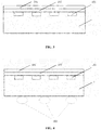
FIG. 1 is a schematic structural view of a fingerprint identification chip and a package structure thereof in the related art; -
FIG. 2 is a schematic structural view of a fingerprint identification chip in the related art; -
FIG. 3 is a schematic structural view of a fingerprint identification module according to an embodiment of the present application; -
FIG. 4 is a schematic structural view of a fingerprint identification module according to an embodiment of the present application; -
FIG. 5 is a schematic structural view of a fingerprint identification module according to an embodiment of the present application; -
FIG. 6 is a schematic structural view of a fingerprint identification module according to an embodiment of the present application; -
FIG. 7 is a schematic structural view of a fingerprint identification module according to an embodiment of the present application. - To make the objectives, technical solutions and advantages of the embodiments of the present application clearer, the technical solutions according to the embodiments of the present application are clearly and thoroughly described with reference to the accompanying drawings of the embodiments of the present application. The described embodiments are merely exemplary ones, but are not all the embodiments of the present application. Based on the embodiments of the present application, all other embodiments derived by persons of ordinary skill in the art without any creative efforts shall fall within the protection scope of the present application.
- The technical solutions of the present application are further described in detail with reference to the specific embodiments.
-
FIG. 1 is a schematic structural view of fingerprint identification chip and a package structure thereof in the related art. As illustrated inFIG. 1 , a package structure of afingerprint identification chip 1 includes asubstrate 201 at the bottom of thefingerprint identification chip 1, and aplastic package 202 surrounding thefingerprint identification chip 1. An upper surface of afingerprint sensing region 101 of thefingerprint identification chip 1 and an upper surface of the plastic package are in the same horizontal plane, such that thefingerprint sensing region 101 is exposed outside the package structure. - Upon completion of chip-exposed packaging, since the fingerprint sensing region of the
fingerprint identification chip 1 is exposed outside the package structure, and in such fabrication processes as downstream module assembling and the like, the exposedfingerprint sensing region 101 of the fingerprint identification chip is easily subject to damages, before such fabrication processes as downstream module assembling and the like, sufficient protections are provided for thefingerprint sensing region 101 of thefingerprint identification chip 1. Specifically, afilm layer 101 is present on an upper surface of thefingerprint sensing region 101 of thefingerprint identification chip 1 upon fabrication of wafer. As illustrated inFIG. 2 , thefilm layer 102 is generally made from lamination of two materials of silicon dioxide (SiO2) and silicon nitride (Si3N4). The lamination thickness ratio of the two materials may be different depending on the fabricators. However, due to restriction of the manufacture process, generally the total thickness is between 1 and 3 µm. Since the thickness of thefilm layer 102 is small, thefilm layer 102 may not provide sufficient protections for thefingerprint sensing region 101 in fabrication processes such as downstream module assembling and the like of thefingerprint identification chip 1. - In view of the above, an embodiment of the present application provides a fingerprint identification module. As illustrated in
FIG. 3 , the fingerprint identification module includes afingerprint identification chip 1 and a package structure for packaging thefingerprint identification chip 1. The package structure leaves thefingerprint sensing region 101 of thefingerprint identification chip 1 exposed. Aprotection layer 301 with a predetermined thickness is arranged on an upper surface of thefilm layer 102 of thefingerprint sensing region 101. Theprotection layer 301 protects thefingerprint sensing region 101 exposed outside the package structure, and enables thefingerprint identification chip 1 to have a predefined fingerprint identification distance. - In the prior art, the film layer on the upper surface of the fingerprint identification chip has a small thickness, and sufficient protections may not be provided for the fabrication processes such as downstream module assembling and the like. Therefore, in this embodiment, the
protection layer 301 is arranged on the upper surface of the film layer of thefingerprint identification region 101 to protect thefingerprint sensing region 101 exposed outside during the subsequent fabrication processes, such that thefingerprint sensing region 101 of the fingerprint identification module is not damaged in the fabrication processes such as downstream module assembling and the like. In this way, the fingerprint identification module has good contamination resistance and scratch resistance, and thus the yield rate of thefingerprint identification chip 1 in the fabrication processes such as downstream assembling and the like is improved. - Meanwhile, to ensure that the
fingerprint identification chip 1 has a predefined fingerprint identification distance, the thickness of theprotection layer 301 is predefined to protect thefingerprint sensing region 101 of thefingerprint identification chip 1 while effective identification of the fingerprint by the fingerprint identification chip is not affected. For example, the thickness of theprotection layer 301 may be predefined according to a fingerprint sensing distance of the fingerprint identification chip and material properties of theprotection layer 301. If the material properties of the protection layer provide good protections for thefingerprint sensing region 101 of thefingerprint identification chip 1, the predefined thickness of theprotection layer 301 may be smaller. - Specifically, in another embodiment of the present application, as illustrated in
FIG. 4 , upon package, the obtained fingerprint identification module not only includes aprotection layer 401, but also includes: asolder ball array 402 electrically connected to an external circuit. Thesolder ball array 402 is arranged under thefingerprint identification chip 1, and is electrically connected to a through-silicon vias structure of thefingerprint identification chip 1 via a solder pad on a lower surface of thefingerprint identification chip 1. - In this embodiment, the solder ball array may be formed by the ball grid array (BGA) process, and the solder balls may be tin balls. The fingerprint identification module is connected to the external circuit via a pin which is the
solder ball array 402. Specifically, thesolder ball array 402 is of a ball shape, to provide a better heat dissipation for thefingerprint identification chip 1. In addition, the life time of thefingerprint identification chip 1 is prolonged, since the solder ball is not subject to deformation and thesolder ball array 402 are sufficiently secure. - In this embodiment, inside the
fingerprint identification chip 1, a through-silicon vias structure (not illustrated in the drawings) formed by the TSV process is present. In thefingerprint identification chip 1, lines are connected to their desired positions via the through-silicon vias structure. Since the through-silicon vias structure is defined inside thefingerprint identification chip 1 and not exposed outside, the through-silicon vias structure does not need to be additionally protected, such that the package volume of thefingerprint identification chip 1 is effectively reduced. - In the fingerprint identification module according to this embodiment, a solder ball array which may be used as the pin may be additionally arranged on the bottom of the
fingerprint identification chip 1. In this way, the obtainedfingerprint identification chip 1 has a minimum volume and a minimum thickness. - Another embodiment of the present application provides a fingerprint identification module. As illustrated in
FIG. 5 , the fingerprint identification module according to this embodiment is a fingerprint identification module obtained through secondary packaging of the fingerprint chip based on the above embodiment. In the secondary packaging, a substrate or a frame may be additionally arranged under thefingerprint identification chip 1, to package the underneath part of thefingerprint identification chip 1. This embodiment gives description using arranging asubstrate 404 as an example. - In this embodiment, the
substrate 404 is arranged under thesolder ball array 402, and the arrangedsubstrate 404 may provide protections for the underneath part of thefingerprint identification chip 1. Acontact array 405 formed by the land grid array (LGA) packaging process is arranged under thesubstrate 404. Thesolder ball array 402 is electrically connected to the external circuit via thecontact array 405. - Specifically, in this embodiment, the
solder ball array 402 is electrically connected to a passageway inside thesubstrate 404. The passageway inside thesubstrate 404 electrically connects thesolder ball array 402 to thecontact array 405, such that thecontact array 405 is used as a pin via which thefingerprint identification chip 1 is connected to the external circuit. - In this embodiment, the area of the
substrate 404 is greater than the area of the lower surface of thefingerprint identification chip 1. The pins of thefingerprint identification chip 1 may be arranged in many ways, and may be adaptive to different external circuits, so as to improve adaptability of the fingerprint identification chip. - Specifically, in this embodiment, the package structure further includes a
plastic package 403. Theplastic package 403 is arranged on thesubstrate 404 and surrounds thefingerprint identification chip 1. - The
plastic package 403 may be made from an epoxy molding compound (EMC), and theplastic package 403 surrounds the fingerprint chip and is molded by cross-linking curing, and thus provides protections for the side surface of thefingerprint identification chip 1. - Specifically, theoretically, an upper surface of the
plastic package 403 and an upper surface of theprotection layer 401 are in the same horizontal plane for the convenience of subsequent processing. However, in the practical process, theprotection layer 401 and theplastic package 403 are separately formed on thefingerprint identification chip 1 by different process steps. As a result, theprotection layer 401 and theplastic package 403 may not be necessarily in the same horizontal plane. In this case, a height difference between theprotection layer 401 and theplastic package 403 may be about 5 µm. - In the fingerprint identification module according to the embodiments of the present application, the package structure of the
fingerprint identification chip 1 includes thesubstrate 404 arranged under thefingerprint identification chip 1, theprotection layer 401 arranged on the upper surface of thefingerprint identification chip 1, and theplastic package 403 surrounding thefingerprint identification chip 1. The package structure contains thefingerprint identification chip 1 therein to provide sufficient protections for thefingerprint identification chip 1. - In the fingerprint identification module according to the embodiments of the present application, based on chip-exposed packaging, protections may be provided for the underneath part of the
fingerprint identification chip 1 by additionally arranging a protection layer on the upper surface of the fingerprint identification chip and arranging asubstrate 404. In this way, the obtained package structure is a substrate-type package structure. - An embodiment of the present application further provides a fingerprint identification module. As illustrated in
FIG. 6 , the fingerprint identification module includes afingerprint identification chip 1 and a package structure for packaging thefingerprint identification chip 1. The package structure leaves afingerprint sensing region 101 of thefingerprint identification chip 1 exposed. An upper surface of a film layer of thefingerprint sensing region 101 has aprotection layer 501 with a predetermined thickness. Theprotection layer 501 is exposed in thefingerprint sensing region 101 outside the package structure and causes thefingerprint identification chip 1 to have a predefined fingerprint identification distance. - Specifically, in this embodiment, a solder pad is arranged on a lower surface of the
fingerprint identification chip 1; asubstrate 505 is arranged under the solder pad; atrench structure 502 causing the fingerprint identification chip to be electrically connected to a circuit on the solder pad is arranged on the fingerprint identification chip; acontact array 506 electrically connected to a peripheral circuit is arranged under thesubstrate 505; and the solder pad is electrically connected to thecontact array 506 such that thefingerprint identification chip 1 is electrically connected to the peripheral circuit via thecontact array 506. - The package structure may include the
substrate 505 arranged under thefingerprint identification chip 1. Thecontact array 506 is formed under thesubstrate 505 via the land grid array (LGA) packaging process. Thefingerprint identification chip 1 is electrically connected to thecontact array 506, and then electrically connected to a peripheral circuit via thecontact array 506. - In this embodiment, a
trench structure 502 is formed on a side surface of thefingerprint identification chip 1 by the trenching process, such that the side surface of thefingerprint identification chip 1 has a stage surface. By means of arranging a distribution layer on thetrench structure 502, a circuit port on the surface of thefingerprint identification chip 1 is led to the stage surface via the distribution layer, and then is electrically connected to a circuit on the solder pad of thefingerprint identification chip 1 via ametal lead 503. Afterwards, the circuit on the solder pad is electrically connected to thecontact array 506 by the redistribution layer (RDL) process. - Specifically, in this embodiment, the lines are connected to their desired positions by the trenching process and the redistribution layer process, and then the
protection layer 501 is machined and formed on the surface of the fingerprint sensing region of thefingerprint identification chip 1. - In this embodiment or other embodiments, the
protection layer 501 is an organic passivation layer or an inorganic passivation layer having the dielectric function. The passivation layer has a thickness of 10 to 20 µm, and has a dielectric constant being greater than 3, to reduce the impacts caused by the passivation layer to the fingerprint identification chip. - The passivation layer is formed by spin coating, spray coating, vapor deposition or mold injection, to ensure that the passivation layer has a predetermined thickness.
- The passivation layer is made from silicon oxide (SiO2), alumina (Al2O3) and the like organic component particles, or resin organic coating. Specifically, if the
protection layer 501 includes an organic material, the properties of the material may be modified by changing the ratio of different organic resins, for example, strength and the like. After the properties of the material are modified, as described above, the predetermined thickness of the protection layer may also be adjusted according to the different properties of the material. - When the
protection layer 501 is formed by the vapor deposition process, since the vapor deposition process is a process of physical and chemical reactions in the vapor phase, a functional or decorative metal, non-metal or compound coating is formed on the upper surface of thefingerprint sensing region 101, the material components only includes inorganic components, but do not include organic components. - Specifically, after the
protection layer 501 is formed by different processes, the physical property and appearance feature of theprotection layer 501 are compatible with the physical property and appearance feature of theplastic package 504 in the package structure of the fingerprint chip. In terms of compatibility of the appearance feature, the color of theprotection layer 501 may be the same as or close to the color of theplastic package 504. Specifically, when theplastic package 504 is an EMC plastic package, the color of theprotection layer 501 may be black, gray or the like that is close to the color of the EMC plastic package. In terms of compatibility of the physical property, the material of theprotection layer 501 and the material of theplastic package 504 have the same or close expansion coefficient and contraction strength, such that when the usage environment of thefingerprint identification chip 1 changes, theprotection layer 501 and theplastic package 504 are constantly in good contact. - The predetermined thickness of the
protection layer 501 is determined based on a plurality of factors, for example, the identification distance of thefingerprint identification chip 1 before packaging, the predefined identification distance of thefingerprint identification chip 1, the material of theprotection layer 501, the application environment of the protection layer and the like. The smaller the predefined fingerprint identification distance of thefingerprint identification chip 1, the greater the thickness of theprotection layer 501. The greater the hardness of theprotection layer 501, the smaller the thickness of theprotection layer 501, and the less abrasiveness or scratch. When theprotection layer 501 is directly used as a working surface in direct contact with a finger, the desired thickness of theprotection layer 501 is greater. After theprotection layer 501 is additionally provided with a cover, when the cover is used as a working surface in direction contact with the finger, the desired thickness of theprotection layer 501 is smaller. - Specifically, in this embodiment, the package structure further includes a
plastic package 504. Theplastic package 504 is arranged on thesubstrate 505 and surrounds thefingerprint identification chip 1. - The
plastic package 504 may be made from an epoxy molding compound (EMC), and theplastic package 504 surrounds the fingerprint chip and is molded by cross-linking curing, and thus provides protections for the side surface of thefingerprint identification chip 1. - Specifically, theoretically, an upper surface of the
plastic package 504 and an upper surface of theprotection layer 501 are in the same horizontal plane for the convenience of subsequent processing. However, in the practical process, theprotection layer 501 and theplastic package 504 are separately formed on thefingerprint identification chip 1 by different process steps. As a result, theprotection layer 501 and theplastic package 504 may not be necessarily in the same horizontal plane. In this case, a height difference between theprotection layer 501 and theplastic package 504 may be about 5 µm. - The above embodiments only give exemplary description by using the chip-exposed packaging or substrate 505-type packaging upon completion of packaging as an example. However, the packaging of the
fingerprint identification chip 1 further includes a frame-type package product. The frame-type package product is similar to the substrate 505-type packaging, which is thus not described herein any further. - The protection layer of the
fingerprint identification chip 1 provides protections for thefingerprint identification chip 1 in fabrication processes such as downstream module assembling and the like upon completion of packaging. However, upon completion of the fabrication processes such as downstream module assembling and the like, thefingerprint identification chip 1 may be put into use. In this case, sufficient protections also need to be provided for thefingerprint identification chip 1. - In another embodiment of the present application, as illustrated in
FIG. 7 , upon completion of packaging of thefingerprint identification chip 1, acover 507 may also be arranged over the protection layer. Thecover 507 is attached to the protection layer via a resin adhesive. Thecover 507 is used as a working surface in contact with a finger. In this case, the passivation layer is a high surface energy passivation layer that is adaptive to the resin adhesive. The surface energy is a unit for measuring the energy on the surface of a solid. The passivation layer having a high surface energy is strongly attached to the adhesive, such that the bonding of the passivation layer and the resin adhesive is more compact. - In this embodiment, when the cover is used as the working surface in contact with the finger during the use of the
fingerprint identification chip 1, thecover 507 needs to have sufficient hardness to provide sufficient protections for thefingerprint identification chip 1 during the use. Specifically, thecover 507 may be made from glass, sapphire or ceramic. - Alternatively, during the use, the protection layer is directly used as the working surface in contact with the finger. During the use, if sufficient protections need to be provided for the
fingerprint identification chip 1, the protection layer needs to have sufficient hardness, thickness and good oleophobic property, hydrophobic property, dust-resistant property, and scratch resistance property. The property of the protection layer may be practiced by using different passivation materials. In addition, during the process of forming the protection layer, machining is carried out such that the protection layer has a specific micro structure, for example, a nano-scale protrusion shape or an increased nano-scale spacing between the protrusions and the like. The strength, oleophobic property, hydrophobic property and the like of the protection layer of thefingerprint identification chip 1 are enhanced by using the micro structure. - The above described device embodiments are merely for illustration purpose only. The modules which are described as separate components may be physically separated or may be not physically separated, and the components which are illustrated as modules may be or may not be physical modules, that is, the components may be located in the same position or may be distributed into a plurality of network modules. A part or all of the modules may be selected according to the actual needs to achieve the objectives of the technical solutions of the embodiments. Persons of ordinary skill in the art may understand and implement the present application without paying any creative effort.
- According to the above embodiments of the present application, a person skilled in the art may clearly understand that the embodiments of the present application may be implemented by means of hardware or by means of software plus a necessary general hardware platform. Based on such understanding, portions of the technical solutions of the present application that essentially contribute to the related art may be embodied in the form of a software product, the computer software product may be stored in a storage medium, such as a ROM/RAM, a magnetic disk, a CD-ROM and the like, including several instructions for causing a computer device (a personal computer, a server, or a network device) to perform the various embodiments of the present application, or certain portions of the method of the embodiments.
- Finally, it should be noted that the above embodiments are merely used to illustrate the technical solutions of the present application rather than limiting the technical solutions of the present application. Although the present application is described in detail with reference to the foregoing embodiments, persons of ordinary skill in the art should understand that they may still make modifications to the technical solutions described in the above embodiments, or make equivalent replacements to some of the technical features; however, such modifications or replacements do not cause the essence of the corresponding technical solutions to depart from the spirit and scope of the technical solutions of the embodiments of the present application.
Claims (17)
- A fingerprint identification module, comprising a fingerprint identification chip and a package structure for packaging the fingerprint identification chip; wherein the package structure leaves a fingerprint sensing region of the fingerprint identification chip exposed, a protection layer with a predetermined thickness being provided on an upper surface of a film layer of the fingerprint sensing region, the protection layer is configured to protect the fingerprint sensing region exposed outside the package structure and cause the fingerprint identification chip to have a predefined fingerprint identification distance.
- The module according to claim 1, further comprising: a solder ball array electrically connected to an external circuit; wherein the solder ball array is arranged under the fingerprint identification chip and is electrically connected to a through-silicon vias structure of the fingerprint identification chip via a solder pad on a lower surface of the fingerprint identification chip, such that the fingerprint identification chip is electrically connected to the external circuit.
- The module according to claim 2, wherein a substrate is arranged under the solder ball array, a contact array is arranged under the substrate, and the solder ball array is electrically connected to the external circuit via the contact array.
- The module according to claim 3, wherein the package structure further comprises a plastic package, the plastic package being arranged on the substrate and surrounding the fingerprint identification chip.
- The module according to claim 4, wherein an upper surface of the plastic package and an upper surface of the protection layer are in the same horizontal plane.
- The module according to claim 1, wherein a solder pad is arranged on a lower surface of the fingerprint identification chip, a substrate being arranged under the solder pad, a trench structure causing the fingerprint identification chip to be electrically connected to a circuit on the solder pad being arranged on the fingerprint identification chip, a contact array electrically connected to a peripheral circuit being arranged under the substrate, the solder pad being electrically connected to the contact array such that the fingerprint identification chip is electrically connected to the peripheral circuit via the contact array.
- The module according to any one of claims 1 to 4, wherein the protection layer is a passivation layer.
- The module according to claim 7, wherein the passivation layer is an organic passivation layer or inorganic passivation layer having a dielectric function.
- The module according to claim 8, wherein the passivation layer has a dielectric constant being greater than 3.
- The module according to claim 7, wherein the passivation layer is formed by spin coating, spray coating, vapor deposition or mold injection.
- The module according to claim 7, wherein the passivation layer has a thickness of 10 to 20 µm.
- The module according to claim 7, wherein a cover is arranged above the passivation layer, the cover being bonded to the passivation layer and used as a working surface for a finger to contact.
- The module according to claim 12, wherein the cover is bonded to the passivation layer via a resin-based adhesive, and the passivation layer is a high surface energy passivation layer that is adaptive to the resin-based adhesive.
- The module according to claim 7, wherein the passivation layer is directly used as a working surface for a finger to contact.
- The module according to claim 1, wherein the fingerprint identification chip comprises any one of a bare chip, a wafer chip and a package chip.
- The module according to claim 1, wherein the package structure comprises a chip-exposed package structure, a substrate-type package structure and a frame-type package structure.
- A package structure of a fingerprint identification chip, wherein the package structure leaves a fingerprint sensing region of the fingerprint identification chip exposed, a protection layer with a predetermined thickness being arranged on an upper surface of a film layer of the fingerprint sensing region, the protection layer protecting the fingerprint sensing region exposed outside the package structure and causing the fingerprint identification chip to have a predefined fingerprint identification distance.
Applications Claiming Priority (1)
| Application Number | Priority Date | Filing Date | Title |
|---|---|---|---|
| PCT/CN2016/104859 WO2018082087A1 (en) | 2016-11-07 | 2016-11-07 | Fingerprint recognition module and fingerprint recognition chip packaging structure |
Publications (3)
| Publication Number | Publication Date |
|---|---|
| EP3418941A1 true EP3418941A1 (en) | 2018-12-26 |
| EP3418941A4 EP3418941A4 (en) | 2019-05-01 |
| EP3418941B1 EP3418941B1 (en) | 2021-08-18 |
Family
ID=62075396
Family Applications (1)
| Application Number | Title | Priority Date | Filing Date |
|---|---|---|---|
| EP16920840.2A Active EP3418941B1 (en) | 2016-11-07 | 2016-11-07 | Fingerprint recognition module and fingerprint recognition chip packaging structure |
Country Status (4)
| Country | Link |
|---|---|
| US (1) | US10810400B2 (en) |
| EP (1) | EP3418941B1 (en) |
| CN (1) | CN108701208B (en) |
| WO (1) | WO2018082087A1 (en) |
Cited By (1)
| Publication number | Priority date | Publication date | Assignee | Title |
|---|---|---|---|---|
| TWI737249B (en) * | 2020-04-02 | 2021-08-21 | 虹晶科技股份有限公司 | Fingerprint identification chip packaging structure and manufacture method thereof |
Families Citing this family (6)
| Publication number | Priority date | Publication date | Assignee | Title |
|---|---|---|---|---|
| CN109376726B (en) * | 2018-12-24 | 2024-04-02 | 苏州科阳半导体有限公司 | Under-screen optical fingerprint chip packaging structure |
| CN210006733U (en) * | 2019-03-04 | 2020-01-31 | Pep创新私人有限公司 | Chip packaging structure |
| CN111126215A (en) * | 2019-12-13 | 2020-05-08 | 维沃移动通信有限公司 | Functional modules and electronic equipment |
| CN113205007B (en) * | 2021-04-14 | 2022-11-15 | 深圳市昊岳科技有限公司 | Biosensor and manufacturing method thereof |
| CN113158884A (en) * | 2021-04-19 | 2021-07-23 | 广东绿展科技有限公司 | Packaging structure of fingerprint identification chip and terminal equipment |
| CN116013872A (en) * | 2022-12-28 | 2023-04-25 | 深圳市汇顶科技股份有限公司 | Packaging structure, packaging method and electronic equipment of a fingerprint identification chip |
Family Cites Families (20)
| Publication number | Priority date | Publication date | Assignee | Title |
|---|---|---|---|---|
| DE102006035644A1 (en) * | 2006-07-31 | 2008-02-14 | Advanced Micro Devices, Inc., Sunnyvale | A method of reducing contamination by providing a polymeric protective layer to be removed during processing of microstructures |
| US20080136012A1 (en) * | 2006-12-08 | 2008-06-12 | Advanced Chip Engineering Technology Inc. | Imagine sensor package and forming method of the same |
| CN102201376B (en) * | 2010-03-22 | 2015-10-14 | 精材科技股份有限公司 | Optical cover plate for packaging, image sensor packaging body and manufacturing method thereof |
| US8603910B2 (en) * | 2012-01-13 | 2013-12-10 | Infineon Technologies Ag | Method of processing a contact pad |
| US9030440B2 (en) * | 2012-05-18 | 2015-05-12 | Apple Inc. | Capacitive sensor packaging |
| US9425092B2 (en) * | 2013-03-15 | 2016-08-23 | Applied Materials, Inc. | Methods for producing interconnects in semiconductor devices |
| EP3072083B1 (en) * | 2013-11-22 | 2018-07-18 | Shenzhen Goodix Technology Co., Ltd. | Secure human fingerprint sensor |
| CN203674206U (en) * | 2014-01-07 | 2014-06-25 | 深圳市汇顶科技股份有限公司 | Wafer level packaging structure and fingerprint identification device |
| TWI485821B (en) * | 2014-02-24 | 2015-05-21 | 新東亞微電子股份有限公司 | Fingerprint identification chip package module and manufacturing method thereof |
| CN104051366B (en) * | 2014-07-01 | 2017-06-20 | 苏州晶方半导体科技股份有限公司 | Fingerprint recognition chip-packaging structure and method for packing |
| CN104201116B (en) * | 2014-09-12 | 2018-04-20 | 苏州晶方半导体科技股份有限公司 | Fingerprint recognition chip packaging method and encapsulating structure |
| CN204179071U (en) * | 2014-09-12 | 2015-02-25 | 苏州晶方半导体科技股份有限公司 | Wafer scale fingerprint recognition chip-packaging structure |
| CN104615979A (en) * | 2015-01-27 | 2015-05-13 | 华进半导体封装先导技术研发中心有限公司 | Fingerprint identification module and encapsulation method thereof, and fingerprint identification module group and encapsulation method thereof |
| CN105990269B (en) * | 2015-03-06 | 2019-03-05 | 吴勇军 | A fingerprint identification chip packaging structure and packaging method thereof |
| CN104851813A (en) * | 2015-05-19 | 2015-08-19 | 苏州晶方半导体科技股份有限公司 | Fingerprint identification chip packaging structure and packaging method |
| US9679187B2 (en) * | 2015-06-17 | 2017-06-13 | Apple Inc. | Finger biometric sensor assembly including direct bonding interface and related methods |
| CN204991696U (en) * | 2015-09-11 | 2016-01-20 | 深圳市汇顶科技股份有限公司 | Sensing chip package subassembly and electronic equipment who has this sensing chip package subassembly |
| CN106601629B (en) * | 2015-10-15 | 2018-11-30 | 力成科技股份有限公司 | Chip packaging structure with protective sheet adhered to chip induction surface |
| CN105552027B (en) * | 2016-02-14 | 2018-08-14 | 武汉华星光电技术有限公司 | The production method and array substrate of array substrate |
| CN206225349U (en) * | 2016-11-07 | 2017-06-06 | 深圳市汇顶科技股份有限公司 | Fingerprint recognition module and fingerprint recognition chip-packaging structure |
-
2016
- 2016-11-07 WO PCT/CN2016/104859 patent/WO2018082087A1/en not_active Ceased
- 2016-11-07 CN CN201680077019.3A patent/CN108701208B/en active Active
- 2016-11-07 EP EP16920840.2A patent/EP3418941B1/en active Active
-
2018
- 2018-09-13 US US16/130,151 patent/US10810400B2/en active Active
Cited By (1)
| Publication number | Priority date | Publication date | Assignee | Title |
|---|---|---|---|---|
| TWI737249B (en) * | 2020-04-02 | 2021-08-21 | 虹晶科技股份有限公司 | Fingerprint identification chip packaging structure and manufacture method thereof |
Also Published As
| Publication number | Publication date |
|---|---|
| US10810400B2 (en) | 2020-10-20 |
| EP3418941B1 (en) | 2021-08-18 |
| WO2018082087A1 (en) | 2018-05-11 |
| US20190012516A1 (en) | 2019-01-10 |
| CN108701208B (en) | 2022-05-06 |
| CN108701208A (en) | 2018-10-23 |
| EP3418941A4 (en) | 2019-05-01 |
Similar Documents
| Publication | Publication Date | Title |
|---|---|---|
| US10810400B2 (en) | Fingerprint identification module and package structure of fingerprint identification chip | |
| US11037819B2 (en) | Wafer level chip scale packaging intermediate structure apparatus and method | |
| US10157811B2 (en) | Chip package and method for forming the same | |
| US11342296B2 (en) | Semiconductor structure, semiconductor package and method of fabricating the same | |
| US10204883B2 (en) | Semiconductor device and manufacturing method thereof | |
| CN206225349U (en) | Fingerprint recognition module and fingerprint recognition chip-packaging structure | |
| US20190131243A1 (en) | Integrated fan-out package and method of fabricating the same | |
| US20210280519A1 (en) | Package structure and semiconductor pacakge | |
| US9337115B2 (en) | Chip package and method for forming the same | |
| US10685896B2 (en) | Integrated circuit package and method of fabricating the same | |
| US10658333B2 (en) | Package structure and method of fabricating the same | |
| US10978408B2 (en) | Semiconductor package and manufacturing method thereof | |
| US20170098589A1 (en) | Fan-out wafer level package structure | |
| US20230245923A1 (en) | Wafer Level Chip Scale Packaging Intermediate Structure Apparatus and Method | |
| CN105489659B (en) | Chip package and manufacturing method thereof | |
| US9711425B2 (en) | Sensing module and method for forming the same | |
| US10636757B2 (en) | Integrated circuit component package and method of fabricating the same | |
| CN108074904B (en) | Electronic package and manufacturing method thereof | |
| US10964656B2 (en) | Semiconductor package and method of manufacturing same | |
| CN106293196B (en) | Composite body of touch panel and sensing chip packaging body module and manufacturing method thereof | |
| US11081435B2 (en) | Package substrate and flip-chip package circuit including the same |
Legal Events
| Date | Code | Title | Description |
|---|---|---|---|
| STAA | Information on the status of an ep patent application or granted ep patent |
Free format text: STATUS: THE INTERNATIONAL PUBLICATION HAS BEEN MADE |
|
| PUAI | Public reference made under article 153(3) epc to a published international application that has entered the european phase |
Free format text: ORIGINAL CODE: 0009012 |
|
| STAA | Information on the status of an ep patent application or granted ep patent |
Free format text: STATUS: REQUEST FOR EXAMINATION WAS MADE |
|
| 17P | Request for examination filed |
Effective date: 20180917 |
|
| AK | Designated contracting states |
Kind code of ref document: A1 Designated state(s): AL AT BE BG CH CY CZ DE DK EE ES FI FR GB GR HR HU IE IS IT LI LT LU LV MC MK MT NL NO PL PT RO RS SE SI SK SM TR |
|
| AX | Request for extension of the european patent |
Extension state: BA ME |
|
| A4 | Supplementary search report drawn up and despatched |
Effective date: 20190403 |
|
| RIC1 | Information provided on ipc code assigned before grant |
Ipc: H01L 23/28 20060101ALI20190328BHEP Ipc: H01L 23/00 20060101ALI20190328BHEP Ipc: G06K 9/00 20060101AFI20190328BHEP |
|
| DAV | Request for validation of the european patent (deleted) | ||
| DAX | Request for extension of the european patent (deleted) | ||
| STAA | Information on the status of an ep patent application or granted ep patent |
Free format text: STATUS: EXAMINATION IS IN PROGRESS |
|
| 17Q | First examination report despatched |
Effective date: 20200930 |
|
| GRAJ | Information related to disapproval of communication of intention to grant by the applicant or resumption of examination proceedings by the epo deleted |
Free format text: ORIGINAL CODE: EPIDOSDIGR1 |
|
| STAA | Information on the status of an ep patent application or granted ep patent |
Free format text: STATUS: GRANT OF PATENT IS INTENDED |
|
| RIC1 | Information provided on ipc code assigned before grant |
Ipc: H01L 23/28 20060101ALI20210312BHEP Ipc: G06K 9/00 20060101AFI20210312BHEP |
|
| GRAP | Despatch of communication of intention to grant a patent |
Free format text: ORIGINAL CODE: EPIDOSNIGR1 |
|
| GRAS | Grant fee paid |
Free format text: ORIGINAL CODE: EPIDOSNIGR3 |
|
| GRAJ | Information related to disapproval of communication of intention to grant by the applicant or resumption of examination proceedings by the epo deleted |
Free format text: ORIGINAL CODE: EPIDOSDIGR1 |
|
| GRAL | Information related to payment of fee for publishing/printing deleted |
Free format text: ORIGINAL CODE: EPIDOSDIGR3 |
|
| STAA | Information on the status of an ep patent application or granted ep patent |
Free format text: STATUS: EXAMINATION IS IN PROGRESS |
|
| INTG | Intention to grant announced |
Effective date: 20210426 |
|
| INTC | Intention to grant announced (deleted) | ||
| GRAP | Despatch of communication of intention to grant a patent |
Free format text: ORIGINAL CODE: EPIDOSNIGR1 |
|
| STAA | Information on the status of an ep patent application or granted ep patent |
Free format text: STATUS: GRANT OF PATENT IS INTENDED |
|
| GRAA | (expected) grant |
Free format text: ORIGINAL CODE: 0009210 |
|
| STAA | Information on the status of an ep patent application or granted ep patent |
Free format text: STATUS: THE PATENT HAS BEEN GRANTED |
|
| INTG | Intention to grant announced |
Effective date: 20210628 |
|
| AK | Designated contracting states |
Kind code of ref document: B1 Designated state(s): AL AT BE BG CH CY CZ DE DK EE ES FI FR GB GR HR HU IE IS IT LI LT LU LV MC MK MT NL NO PL PT RO RS SE SI SK SM TR |
|
| REG | Reference to a national code |
Ref country code: GB Ref legal event code: FG4D |
|
| REG | Reference to a national code |
Ref country code: CH Ref legal event code: EP |
|
| REG | Reference to a national code |
Ref country code: DE Ref legal event code: R096 Ref document number: 602016062573 Country of ref document: DE |
|
| REG | Reference to a national code |
Ref country code: IE Ref legal event code: FG4D Ref country code: AT Ref legal event code: REF Ref document number: 1422292 Country of ref document: AT Kind code of ref document: T Effective date: 20210915 |
|
| REG | Reference to a national code |
Ref country code: DE Ref legal event code: R079 Ref document number: 602016062573 Country of ref document: DE Free format text: PREVIOUS MAIN CLASS: G06K0009000000 Ipc: G06V0010000000 |
|
| REG | Reference to a national code |
Ref country code: LT Ref legal event code: MG9D |
|
| REG | Reference to a national code |
Ref country code: NL Ref legal event code: MP Effective date: 20210818 |
|
| REG | Reference to a national code |
Ref country code: AT Ref legal event code: MK05 Ref document number: 1422292 Country of ref document: AT Kind code of ref document: T Effective date: 20210818 |
|
| PG25 | Lapsed in a contracting state [announced via postgrant information from national office to epo] |
Ref country code: BG Free format text: LAPSE BECAUSE OF FAILURE TO SUBMIT A TRANSLATION OF THE DESCRIPTION OR TO PAY THE FEE WITHIN THE PRESCRIBED TIME-LIMIT Effective date: 20211118 Ref country code: AT Free format text: LAPSE BECAUSE OF FAILURE TO SUBMIT A TRANSLATION OF THE DESCRIPTION OR TO PAY THE FEE WITHIN THE PRESCRIBED TIME-LIMIT Effective date: 20210818 Ref country code: LT Free format text: LAPSE BECAUSE OF FAILURE TO SUBMIT A TRANSLATION OF THE DESCRIPTION OR TO PAY THE FEE WITHIN THE PRESCRIBED TIME-LIMIT Effective date: 20210818 Ref country code: PT Free format text: LAPSE BECAUSE OF FAILURE TO SUBMIT A TRANSLATION OF THE DESCRIPTION OR TO PAY THE FEE WITHIN THE PRESCRIBED TIME-LIMIT Effective date: 20211220 Ref country code: NO Free format text: LAPSE BECAUSE OF FAILURE TO SUBMIT A TRANSLATION OF THE DESCRIPTION OR TO PAY THE FEE WITHIN THE PRESCRIBED TIME-LIMIT Effective date: 20211118 Ref country code: HR Free format text: LAPSE BECAUSE OF FAILURE TO SUBMIT A TRANSLATION OF THE DESCRIPTION OR TO PAY THE FEE WITHIN THE PRESCRIBED TIME-LIMIT Effective date: 20210818 Ref country code: ES Free format text: LAPSE BECAUSE OF FAILURE TO SUBMIT A TRANSLATION OF THE DESCRIPTION OR TO PAY THE FEE WITHIN THE PRESCRIBED TIME-LIMIT Effective date: 20210818 Ref country code: FI Free format text: LAPSE BECAUSE OF FAILURE TO SUBMIT A TRANSLATION OF THE DESCRIPTION OR TO PAY THE FEE WITHIN THE PRESCRIBED TIME-LIMIT Effective date: 20210818 Ref country code: RS Free format text: LAPSE BECAUSE OF FAILURE TO SUBMIT A TRANSLATION OF THE DESCRIPTION OR TO PAY THE FEE WITHIN THE PRESCRIBED TIME-LIMIT Effective date: 20210818 Ref country code: SE Free format text: LAPSE BECAUSE OF FAILURE TO SUBMIT A TRANSLATION OF THE DESCRIPTION OR TO PAY THE FEE WITHIN THE PRESCRIBED TIME-LIMIT Effective date: 20210818 |
|
| PG25 | Lapsed in a contracting state [announced via postgrant information from national office to epo] |
Ref country code: PL Free format text: LAPSE BECAUSE OF FAILURE TO SUBMIT A TRANSLATION OF THE DESCRIPTION OR TO PAY THE FEE WITHIN THE PRESCRIBED TIME-LIMIT Effective date: 20210818 Ref country code: LV Free format text: LAPSE BECAUSE OF FAILURE TO SUBMIT A TRANSLATION OF THE DESCRIPTION OR TO PAY THE FEE WITHIN THE PRESCRIBED TIME-LIMIT Effective date: 20210818 Ref country code: GR Free format text: LAPSE BECAUSE OF FAILURE TO SUBMIT A TRANSLATION OF THE DESCRIPTION OR TO PAY THE FEE WITHIN THE PRESCRIBED TIME-LIMIT Effective date: 20211119 |
|
| PG25 | Lapsed in a contracting state [announced via postgrant information from national office to epo] |
Ref country code: NL Free format text: LAPSE BECAUSE OF FAILURE TO SUBMIT A TRANSLATION OF THE DESCRIPTION OR TO PAY THE FEE WITHIN THE PRESCRIBED TIME-LIMIT Effective date: 20210818 |
|
| PG25 | Lapsed in a contracting state [announced via postgrant information from national office to epo] |
Ref country code: DK Free format text: LAPSE BECAUSE OF FAILURE TO SUBMIT A TRANSLATION OF THE DESCRIPTION OR TO PAY THE FEE WITHIN THE PRESCRIBED TIME-LIMIT Effective date: 20210818 |
|
| REG | Reference to a national code |
Ref country code: DE Ref legal event code: R097 Ref document number: 602016062573 Country of ref document: DE |
|
| PG25 | Lapsed in a contracting state [announced via postgrant information from national office to epo] |
Ref country code: SM Free format text: LAPSE BECAUSE OF FAILURE TO SUBMIT A TRANSLATION OF THE DESCRIPTION OR TO PAY THE FEE WITHIN THE PRESCRIBED TIME-LIMIT Effective date: 20210818 Ref country code: SK Free format text: LAPSE BECAUSE OF FAILURE TO SUBMIT A TRANSLATION OF THE DESCRIPTION OR TO PAY THE FEE WITHIN THE PRESCRIBED TIME-LIMIT Effective date: 20210818 Ref country code: RO Free format text: LAPSE BECAUSE OF FAILURE TO SUBMIT A TRANSLATION OF THE DESCRIPTION OR TO PAY THE FEE WITHIN THE PRESCRIBED TIME-LIMIT Effective date: 20210818 Ref country code: EE Free format text: LAPSE BECAUSE OF FAILURE TO SUBMIT A TRANSLATION OF THE DESCRIPTION OR TO PAY THE FEE WITHIN THE PRESCRIBED TIME-LIMIT Effective date: 20210818 Ref country code: CZ Free format text: LAPSE BECAUSE OF FAILURE TO SUBMIT A TRANSLATION OF THE DESCRIPTION OR TO PAY THE FEE WITHIN THE PRESCRIBED TIME-LIMIT Effective date: 20210818 Ref country code: AL Free format text: LAPSE BECAUSE OF FAILURE TO SUBMIT A TRANSLATION OF THE DESCRIPTION OR TO PAY THE FEE WITHIN THE PRESCRIBED TIME-LIMIT Effective date: 20210818 |
|
| PLBE | No opposition filed within time limit |
Free format text: ORIGINAL CODE: 0009261 |
|
| STAA | Information on the status of an ep patent application or granted ep patent |
Free format text: STATUS: NO OPPOSITION FILED WITHIN TIME LIMIT |
|
| PG25 | Lapsed in a contracting state [announced via postgrant information from national office to epo] |
Ref country code: MC Free format text: LAPSE BECAUSE OF FAILURE TO SUBMIT A TRANSLATION OF THE DESCRIPTION OR TO PAY THE FEE WITHIN THE PRESCRIBED TIME-LIMIT Effective date: 20210818 |
|
| REG | Reference to a national code |
Ref country code: CH Ref legal event code: PL |
|
| 26N | No opposition filed |
Effective date: 20220519 |
|
| PG25 | Lapsed in a contracting state [announced via postgrant information from national office to epo] |
Ref country code: LU Free format text: LAPSE BECAUSE OF NON-PAYMENT OF DUE FEES Effective date: 20211107 Ref country code: IT Free format text: LAPSE BECAUSE OF FAILURE TO SUBMIT A TRANSLATION OF THE DESCRIPTION OR TO PAY THE FEE WITHIN THE PRESCRIBED TIME-LIMIT Effective date: 20210818 Ref country code: BE Free format text: LAPSE BECAUSE OF NON-PAYMENT OF DUE FEES Effective date: 20211130 |
|
| REG | Reference to a national code |
Ref country code: BE Ref legal event code: MM Effective date: 20211130 |
|
| PG25 | Lapsed in a contracting state [announced via postgrant information from national office to epo] |
Ref country code: SI Free format text: LAPSE BECAUSE OF FAILURE TO SUBMIT A TRANSLATION OF THE DESCRIPTION OR TO PAY THE FEE WITHIN THE PRESCRIBED TIME-LIMIT Effective date: 20210818 Ref country code: LI Free format text: LAPSE BECAUSE OF NON-PAYMENT OF DUE FEES Effective date: 20211130 Ref country code: CH Free format text: LAPSE BECAUSE OF NON-PAYMENT OF DUE FEES Effective date: 20211130 |
|
| PG25 | Lapsed in a contracting state [announced via postgrant information from national office to epo] |
Ref country code: IE Free format text: LAPSE BECAUSE OF NON-PAYMENT OF DUE FEES Effective date: 20211107 |
|
| PG25 | Lapsed in a contracting state [announced via postgrant information from national office to epo] |
Ref country code: FR Free format text: LAPSE BECAUSE OF NON-PAYMENT OF DUE FEES Effective date: 20211130 |
|
| PG25 | Lapsed in a contracting state [announced via postgrant information from national office to epo] |
Ref country code: CY Free format text: LAPSE BECAUSE OF FAILURE TO SUBMIT A TRANSLATION OF THE DESCRIPTION OR TO PAY THE FEE WITHIN THE PRESCRIBED TIME-LIMIT Effective date: 20210818 |
|
| PG25 | Lapsed in a contracting state [announced via postgrant information from national office to epo] |
Ref country code: HU Free format text: LAPSE BECAUSE OF FAILURE TO SUBMIT A TRANSLATION OF THE DESCRIPTION OR TO PAY THE FEE WITHIN THE PRESCRIBED TIME-LIMIT; INVALID AB INITIO Effective date: 20161107 |
|
| PG25 | Lapsed in a contracting state [announced via postgrant information from national office to epo] |
Ref country code: MK Free format text: LAPSE BECAUSE OF FAILURE TO SUBMIT A TRANSLATION OF THE DESCRIPTION OR TO PAY THE FEE WITHIN THE PRESCRIBED TIME-LIMIT Effective date: 20210818 |
|
| PG25 | Lapsed in a contracting state [announced via postgrant information from national office to epo] |
Ref country code: TR Free format text: LAPSE BECAUSE OF FAILURE TO SUBMIT A TRANSLATION OF THE DESCRIPTION OR TO PAY THE FEE WITHIN THE PRESCRIBED TIME-LIMIT Effective date: 20210818 |
|
| PG25 | Lapsed in a contracting state [announced via postgrant information from national office to epo] |
Ref country code: MT Free format text: LAPSE BECAUSE OF FAILURE TO SUBMIT A TRANSLATION OF THE DESCRIPTION OR TO PAY THE FEE WITHIN THE PRESCRIBED TIME-LIMIT Effective date: 20210818 |
|
| PGFP | Annual fee paid to national office [announced via postgrant information from national office to epo] |
Ref country code: DE Payment date: 20251111 Year of fee payment: 10 |
|
| PGFP | Annual fee paid to national office [announced via postgrant information from national office to epo] |
Ref country code: GB Payment date: 20251114 Year of fee payment: 10 |