EP3415465B1 - Mikronadeln - Google Patents
Mikronadeln Download PDFInfo
- Publication number
- EP3415465B1 EP3415465B1 EP18177390.4A EP18177390A EP3415465B1 EP 3415465 B1 EP3415465 B1 EP 3415465B1 EP 18177390 A EP18177390 A EP 18177390A EP 3415465 B1 EP3415465 B1 EP 3415465B1
- Authority
- EP
- European Patent Office
- Prior art keywords
- etch
- microneedles
- plasma etch
- mask
- front face
- Prior art date
- Legal status (The legal status is an assumption and is not a legal conclusion. Google has not performed a legal analysis and makes no representation as to the accuracy of the status listed.)
- Active
Links
Images




Classifications
-
- B—PERFORMING OPERATIONS; TRANSPORTING
- B81—MICROSTRUCTURAL TECHNOLOGY
- B81C—PROCESSES OR APPARATUS SPECIALLY ADAPTED FOR THE MANUFACTURE OR TREATMENT OF MICROSTRUCTURAL DEVICES OR SYSTEMS
- B81C1/00—Manufacture or treatment of devices or systems in or on a substrate
- B81C1/00015—Manufacture or treatment of devices or systems in or on a substrate for manufacturing microsystems
- B81C1/00023—Manufacture or treatment of devices or systems in or on a substrate for manufacturing microsystems without movable or flexible elements
- B81C1/00111—Tips, pillars, i.e. raised structures
-
- A—HUMAN NECESSITIES
- A61—MEDICAL OR VETERINARY SCIENCE; HYGIENE
- A61M—DEVICES FOR INTRODUCING MEDIA INTO, OR ONTO, THE BODY; DEVICES FOR TRANSDUCING BODY MEDIA OR FOR TAKING MEDIA FROM THE BODY; DEVICES FOR PRODUCING OR ENDING SLEEP OR STUPOR
- A61M37/00—Other apparatus for introducing media into the body; Percutany, i.e. introducing medicines into the body by diffusion through the skin
- A61M37/0015—Other apparatus for introducing media into the body; Percutany, i.e. introducing medicines into the body by diffusion through the skin by using microneedles
-
- A—HUMAN NECESSITIES
- A61—MEDICAL OR VETERINARY SCIENCE; HYGIENE
- A61K—PREPARATIONS FOR MEDICAL, DENTAL OR TOILETRY PURPOSES
- A61K9/00—Medicinal preparations characterised by special physical form
- A61K9/0012—Galenical forms characterised by the site of application
- A61K9/0019—Injectable compositions; Intramuscular, intravenous, arterial, subcutaneous administration; Compositions to be administered through the skin in an invasive manner
- A61K9/0021—Intradermal administration, e.g. through microneedle arrays or needleless injectors
-
- H—ELECTRICITY
- H10—SEMICONDUCTOR DEVICES; ELECTRIC SOLID-STATE DEVICES NOT OTHERWISE PROVIDED FOR
- H10P—GENERIC PROCESSES OR APPARATUS FOR THE MANUFACTURE OR TREATMENT OF DEVICES COVERED BY CLASS H10
- H10P50/00—Etching of wafers, substrates or parts of devices
- H10P50/20—Dry etching; Plasma etching; Reactive-ion etching
- H10P50/24—Dry etching; Plasma etching; Reactive-ion etching of semiconductor materials
- H10P50/242—Dry etching; Plasma etching; Reactive-ion etching of semiconductor materials of Group IV materials
-
- H—ELECTRICITY
- H10—SEMICONDUCTOR DEVICES; ELECTRIC SOLID-STATE DEVICES NOT OTHERWISE PROVIDED FOR
- H10P—GENERIC PROCESSES OR APPARATUS FOR THE MANUFACTURE OR TREATMENT OF DEVICES COVERED BY CLASS H10
- H10P50/00—Etching of wafers, substrates or parts of devices
- H10P50/20—Dry etching; Plasma etching; Reactive-ion etching
- H10P50/24—Dry etching; Plasma etching; Reactive-ion etching of semiconductor materials
- H10P50/242—Dry etching; Plasma etching; Reactive-ion etching of semiconductor materials of Group IV materials
- H10P50/244—Dry etching; Plasma etching; Reactive-ion etching of semiconductor materials of Group IV materials comprising alternated and repeated etching and passivation steps
-
- H—ELECTRICITY
- H10—SEMICONDUCTOR DEVICES; ELECTRIC SOLID-STATE DEVICES NOT OTHERWISE PROVIDED FOR
- H10P—GENERIC PROCESSES OR APPARATUS FOR THE MANUFACTURE OR TREATMENT OF DEVICES COVERED BY CLASS H10
- H10P76/00—Manufacture or treatment of masks on semiconductor bodies, e.g. by lithography or photolithography
- H10P76/40—Manufacture or treatment of masks on semiconductor bodies, e.g. by lithography or photolithography of masks comprising inorganic materials
- H10P76/408—Manufacture or treatment of masks on semiconductor bodies, e.g. by lithography or photolithography of masks comprising inorganic materials characterised by their sizes, orientations, dispositions, behaviours or shapes
- H10P76/4085—Manufacture or treatment of masks on semiconductor bodies, e.g. by lithography or photolithography of masks comprising inorganic materials characterised by their sizes, orientations, dispositions, behaviours or shapes characterised by the processes involved to create the masks
-
- A—HUMAN NECESSITIES
- A61—MEDICAL OR VETERINARY SCIENCE; HYGIENE
- A61M—DEVICES FOR INTRODUCING MEDIA INTO, OR ONTO, THE BODY; DEVICES FOR TRANSDUCING BODY MEDIA OR FOR TAKING MEDIA FROM THE BODY; DEVICES FOR PRODUCING OR ENDING SLEEP OR STUPOR
- A61M37/00—Other apparatus for introducing media into the body; Percutany, i.e. introducing medicines into the body by diffusion through the skin
- A61M37/0015—Other apparatus for introducing media into the body; Percutany, i.e. introducing medicines into the body by diffusion through the skin by using microneedles
- A61M2037/0023—Drug applicators using microneedles
-
- A—HUMAN NECESSITIES
- A61—MEDICAL OR VETERINARY SCIENCE; HYGIENE
- A61M—DEVICES FOR INTRODUCING MEDIA INTO, OR ONTO, THE BODY; DEVICES FOR TRANSDUCING BODY MEDIA OR FOR TAKING MEDIA FROM THE BODY; DEVICES FOR PRODUCING OR ENDING SLEEP OR STUPOR
- A61M37/00—Other apparatus for introducing media into the body; Percutany, i.e. introducing medicines into the body by diffusion through the skin
- A61M37/0015—Other apparatus for introducing media into the body; Percutany, i.e. introducing medicines into the body by diffusion through the skin by using microneedles
- A61M2037/003—Other apparatus for introducing media into the body; Percutany, i.e. introducing medicines into the body by diffusion through the skin by using microneedles having a lumen
-
- A—HUMAN NECESSITIES
- A61—MEDICAL OR VETERINARY SCIENCE; HYGIENE
- A61M—DEVICES FOR INTRODUCING MEDIA INTO, OR ONTO, THE BODY; DEVICES FOR TRANSDUCING BODY MEDIA OR FOR TAKING MEDIA FROM THE BODY; DEVICES FOR PRODUCING OR ENDING SLEEP OR STUPOR
- A61M37/00—Other apparatus for introducing media into the body; Percutany, i.e. introducing medicines into the body by diffusion through the skin
- A61M37/0015—Other apparatus for introducing media into the body; Percutany, i.e. introducing medicines into the body by diffusion through the skin by using microneedles
- A61M2037/0053—Methods for producing microneedles
-
- A—HUMAN NECESSITIES
- A61—MEDICAL OR VETERINARY SCIENCE; HYGIENE
- A61M—DEVICES FOR INTRODUCING MEDIA INTO, OR ONTO, THE BODY; DEVICES FOR TRANSDUCING BODY MEDIA OR FOR TAKING MEDIA FROM THE BODY; DEVICES FOR PRODUCING OR ENDING SLEEP OR STUPOR
- A61M2205/00—General characteristics of the apparatus
- A61M2205/02—General characteristics of the apparatus characterised by a particular materials
- A61M2205/0244—Micromachined materials, e.g. made from silicon wafers, microelectromechanical systems [MEMS] or comprising nanotechnology
-
- B—PERFORMING OPERATIONS; TRANSPORTING
- B81—MICROSTRUCTURAL TECHNOLOGY
- B81B—MICROSTRUCTURAL DEVICES OR SYSTEMS, e.g. MICROMECHANICAL DEVICES
- B81B1/00—Devices without movable or flexible elements, e.g. microcapillary devices
- B81B1/006—Microdevices formed as a single homogeneous piece, i.e. wherein the mechanical function is obtained by the use of the device, e.g. cutters
- B81B1/008—Microtips
-
- B—PERFORMING OPERATIONS; TRANSPORTING
- B81—MICROSTRUCTURAL TECHNOLOGY
- B81B—MICROSTRUCTURAL DEVICES OR SYSTEMS, e.g. MICROMECHANICAL DEVICES
- B81B2201/00—Specific applications of microelectromechanical systems
- B81B2201/05—Microfluidics
- B81B2201/055—Microneedles
-
- B—PERFORMING OPERATIONS; TRANSPORTING
- B81—MICROSTRUCTURAL TECHNOLOGY
- B81C—PROCESSES OR APPARATUS SPECIALLY ADAPTED FOR THE MANUFACTURE OR TREATMENT OF MICROSTRUCTURAL DEVICES OR SYSTEMS
- B81C1/00—Manufacture or treatment of devices or systems in or on a substrate
- B81C1/00436—Shaping materials, i.e. techniques for structuring the substrate or the layers on the substrate
- B81C1/00523—Etching material
- B81C1/00531—Dry etching
Definitions
- This invention relates to a method of manufacturing a plurality of microneedles.
- Microneedles are substantially smaller than traditional hypodermic needles, being fabricated on the micro scale. Microneedles have been fabricated using various methods and from various materials such as metals, silicon, silicon dioxide, polymeric materials, and glass.
- the mechanism of drug delivery is not based on diffusion as it is in other transdermal drug delivery products. Instead, the mechanism of drug delivery is based on a temporary mechanical disruption of the skin and the placement of the drug within the epidermis. In this way, the drug can more readily reach its site of action.
- the drugs may be encapsulated within the microneedles, which are then inserted into the skin and thereafter release the drug.
- Microneedles can be fabricated in a single process, and this can lead to high accuracy, good reproducibility, and moderate fabrication costs. Microneedles are also capable of accurate dosing, local delivery, and enhancing biological drug stability through the storage of the drugs in a micro volume that can be precisely controlled. Microneedles can also enable complex drug release patterns to be achieved. Microneedles with a length of a few hundred microns only penetrate into the superficial layers of the skin where the density of nerve receptors is low. As a consequence, the insertion of microneedles into skin is perceived as painless. Skin penetration depth requirements typically vary from ⁇ 300 microns to 500 microns depending on patient age, injection site, and application.
- Microneedles fabricated from silicon constitute a promising area of development.
- process techniques for fabricating wafer-scale silicon based hollow microneedles by plasma etch process techniques have to date been prone to mechanical failure.
- microneedles of this type have limited flexibility in terms of length and pitch variation, and also do not penetrate the skin reliably. It would be desirable to produce microneedles of this type which are bevelled. Bevelled microneedles would allow the needle to easily penetrate the skin and also create minimum skin trauma.
- the present inventors have realised that what is needed is a method of manufacture that can form silicon microneedles having a controllable bevel angle which is user selectable and independent of the crystallographic orientation of the substrate.
- a related requirement is for silicon microneedles that are reliably capable of withstanding the insertion forces that are typical encountered when entering skin without damage.
- the present invention addresses these needs and requirements.
- a method of manufacturing a plurality of silicon microneedles which have a bevelled tip comprising the steps of:
- the present invention can enable arrays of microneedles to be manufactured with improved design flexibility and with better control over the characteristics of the array. For example, shallow bevel angles are generally more suited to applications in which drugs or cells are injected to deeper layers of epidermis. Steeper bevel angles can give rise to arrays of microneedles having a reduced pitch. A further advantage is that reductions in processing times can be achieved over techniques that use a wet etch. A further advantage still is that the present invention produces microneedles having advantageous tip shapes. In particular, a tip shape may be produced having an 'asymmetrical' bevel shape in which the tip has a sharp point which is in direct connection with an upstanding sidewall of the microneedle. Microneedles of this type have excellent penetration properties.
- the microneedles are generally less than 3000 microns in length and may be less than 1000 microns in length.
- the microneedles are generally greater than 100microns in length.
- the microneedles have a length of ⁇ 300-800 micron.
- the SF 6 based plasma etch may be formed in a gaseous mixture comprising SF 6 and a sidewall passivation precursor.
- the sidewall passivation precursor may be at least one of C 4 F 8 and CHF 3 .
- the gaseous mixture may consist essentially of SF 6 , CHF 3 and C 4 F 8 .
- the gaseous mixture may further comprise O 2 .
- the gaseous mixture may consist essentially of SF 6 , O 2 and C 4 F 8 .
- the SF 6 based plasma etch may be formed in a gaseous mixture comprising SF 6 and an inert diluent.
- the inert diluent may be a Noble gas such as Ar.
- the gaseous mixture may consist essentially of SF 6 , O 2 , C 4 F 8 and Ar.
- the DRIE plasma etch of the etched front face may be an anisotropic cyclical etch and deposition process.
- a cyclical etch and deposition process of the type commonly known as the 'Bosch process' may be used.
- Exemplary references are US 5501893 , US 7648611 and US 8133349 , the entire contents of which are herein incorporated by reference.
- the first mask arrangement may be an oxide mask.
- the oxide mask may be a thermal oxide mask.
- the second mask arrangement may comprise a plurality of hard masks.
- the hard masks may be oxide masks.
- the second mask arrangement may be deposited onto the etch features by PE-CVD (plasma enhanced chemical vapour deposition). This is a suitable way of depositing hard masks, such as oxide hard masks.
- the second mask arrangement may comprise a photoresist or a plurality of metal masks.
- front side plasma etching of the second mask using the DRIE anisotropic plasma etch process takes place to achieve a front side cavity etch.
- the method may further comprise a step of performing a DRIE plasma etch of the rear face to form a plurality of channels in the silicon substrate which are positioned so that, after the plurality of microneedles are formed, the channels act as bore passages extending through the microneedles.
- the DRIE plasma etch of the rear face may be a cyclical etch and deposition process. A cyclical etch and deposition process of the type commonly known as the 'Bosch process' may be used.
- the step of performing a DRIE plasma etch of the rear face may be performed prior to the step of performing a DRIE plasma etch of the etched front face.
- the step of performing a DRIE plasma etch of the rear face may be performed after the step of performing a DRIE plasma etch of the etched front face.
- the steps of performing a DRIE plasma etch of the rear face and of performing a DRIE plasma etch of the etched front face are interchangeable.
- a third mask arrangement may be formed on the back face prior to the step of performing a DRIE plasma etch of the back face.
- the third mask arrangement is aligned with corresponding features on the second mask.
- the third mask arrangement may define a plurality of gaps which correspond to the locations of the plurality of channels in the silicon substrate.
- the third mask arrangement may comprise a hard mask, which may be an oxide mask.
- the third mask arrangement may be deposited onto the back face by PE-CVD. This is a suitable way of depositing a hard mask, such as an oxide mask.
- the third mask arrangement may comprise a photoresist or a metal mask.
- the SF 6 based plasma etch of the first face through the gaps in the first mask arrangement provides one or more etch features having a pair of opposed sloping faces.
- the second mask arrangement may be formed only on one of the pair of opposed sloping faces of each etch feature.
- the bevelled tips of the microneedles may be formed as single bevel structures.
- the bevelled tips of the microneedles may be formed as double bevel structures.
- Double bevel structures can provide enhanced skin penetration performance.
- Double bevel structures may be formed by controlling etch conditions during the step of performing a SF 6 based plasma etch of the front face.
- the step of performing a SF 6 based plasma etch of the front face may produce single bevel structures. Double bevel structures may then be produced during the step of performing a DRIE plasma etch of the etched front face.
- the second mask arrangement may comprise oxide masks having a thickness in the range 3 to 5 microns. This is an effective way of producing a double bevel structure.
- the DRIE plasma etch of the etched front face may form one or more ridge structures which are spaced apart from the microneedles.
- the ridge structures can provide a more robust structure which is better able to withstand shear forces.
- Each microneedle may be spaced 100 to 1000 microns, preferably 100 to 600 microns, apart from its nearest ridge structure.
- a plurality of interconnected ridge structures may be formed to provide a plurality of microneedle surrounding fence structures each of which surround and are spaced apart from a microneedle.
- the ridge structures may be formed in the following way:
- the bevelled tips of the microneedles may have a bevel angle in the range 50 to 85°.
- the bevelled tips of the microneedles may have a bevel angle of at least 60°.
- the bevel angle may be at least 70°.
- the bevel angle may be 85° or less.
- the bevelled tip is pointed.
- the bevelled tip may be diamond shaped.
- the gaps defined by the first mask arrangement may each have a width.
- the etch features may each have a base width.
- the base width of each etch feature may be substantially equal to the width of its corresponding gap in the first mask arrangement.
- the base width of each etch feature is within 10% of the width of its corresponding gap in the first mask arrangement.
- the microneedles of the invention can be used in a wide range of applications.
- the microneedles may be hollow, pocketed or solid.
- the microneedles may deliver any desired beneficial substance, such as a drug, cells or other therapeutic substance, when inserted into the skin.
- the microneedles might instead not be used to deliver a beneficial substance.
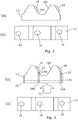
- Figures 1 to 5 show steps in a representative but non-limiting method of the invention.
- Figure 1A shows a portion of a first mask 10 which is formed on a silicon substrate 12.
- the first mask 10 defines a plurality of apertures 14 to reveal exposed portions of a front face of the silicon substrate 12.
- the first mask 10 as shown in Figure 1A consists of a row of apertures 14. As will be explained below, this gives rise to a row of microneedles.
- the more complicated first masks of this type give rise to an array of microneedles having both rows and columns of microneedles.
- the first mask can take many different forms depending on the preferred form of the microneedles desired for any particular application.
- FIG. 1B is a cross sectional view of the silicon substrate/first mask towards the end of the SF 6 based plasma etch, at which point a plurality of etch features 16 have been formed which comprise a pair of opposed sloping faces 16A, 16B. It can be seen that the SF 6 based plasma etch undercuts the first mask 10. The undercut is the amount of lateral etching underneath the mask. In practice, the undercut achieved is at least 10% of the depth of a corresponding etch feature 16.
- the first mask 10 is removed and second masks 18 are formed on one sloping face 16A of the pairs of opposing sloping faces 16A, 16B ( Figures 2A and B ).
- the other sloping face 16B of a pair is not protected by a mask.
- a third mask 20 is formed on the rear face 12A of the silicon substrate 12.
- the third mask 20 is formed with a plurality of apertures 20a in the mask which are aligned with the locations of the second mask 18 on the sloping faces 16A.
- a backside plasma etch 21 of the masked rear face 12A of the silicon substrate is then performed to form a plurality of bore channels 22 which extend from the apertures 20 through the silicon substrate 12 to reach the second masks 18.
- the plasma etch used to form the bore channels 22 can be any convenient etch process. It is very convenient to use a DRIE etch such as a Bosch type etch.
- a DRIE plasma etch of the front side of the silicon substrate 12 plasma etch is performed.
- Figures 4A and B show the DRIE plasma etch 24 of the front face of the silicon substrate 12.
- the plasma etch 24 etches the bulk silicon around the second masks 18 to leave a plurality of bevelled microneedle structures 26 upstanding from a base layer 28. It will be apparent that the plasma etch 24 can be controlled so as to control the depth of the base layer 28 and the height of the microneedle structures 26.
- the plasma etch 24 also forms a plurality of ridge structures 30 which are spaced from the microneedle structures 26.
- the ridge structures are associated with the etching of portions of the front face of the silicon substrate 12 which at least include the sloping faces 16B.
- the second masks 18 are then removed to produce the microneedle array 32 shown in Figures 5A and B .
- the microneedle array 32 comprises a plurality of bevelled microneedle structures 26.
- the microneedle structures 26 are hollow due to the presence of bore channels 20 extending therethrough.
- the embodiment shown in Figures 5A and B also comprises the plurality of ridge structures 30. In practice, it is usual for the microneedle array to be formed with a far greater number of microneedle structures.
- the third mask 20 on the rear face 12A remains in place. Optionally, the third mask 20 could be removed.
- the present invention provides a SF 6 based dry plasma etch which can be used to create sloped sidewalls which can be further processed to provide a plurality of bevelled microneedles.
- suitable SF 6 based gas mixtures include: SF 6 /O 2 /C 4 F 8 ; SF 6 /O 2 /C 4 F 8 /Ar; SF 6 /O 2 /A r ; and SF 6 /CHF 3 /C 4 F 8 .
- Other SF 6 based gaseous compositions might be used.
- compositions may be with or without oxygen and/or with or without an inert diluent such as argon.
- the relative proportion of the constituents may also be varied in order to achieve desired profiles.
- the SF 6 based plasma forms the basis of an isotropic etch. It is desirable to add a constituent such as C 4 F 8 and/or CHF 3 to achieve some sidewall passivation.
- the sidewall passivation restricts lateral etching and helps to maintain a profile which is free from "overhang".
- the etch achieves a large undercut below the first mask, but the sidewalls become passivated due to ion-assisted migration or diffusion of polymeric moieties from the base of the etch feature to the sidewalls.
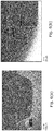
- Figures 6A and B show SEMs of etch features achieved using typical process conditions for the SF 6 / C 4 F 8 based first plasma etch
- the first mask can be clearly seen as essentially horizontal white lines towards the top of each Figure 6A and B.
- Figure 6A shows a gap defined by the first mask.
- the width of the opening defined by the first mask is similar to the base width of the etch feature. This is a typical but non-limiting result.
- the SF 6 based plasma etch has produced a substantially flat base with a pair of opposed sloping sidewalls having a 60.9° profile angle.
- the SF 6 based plasma etch has resulted in an undercut of the first mask which is greater than 200 microns.
- a sloping sidewall is produced having a profile angle of 69.1° and a depth of 188 microns.
- Typical process contents for the SF 6 based plasma etch are: platen temperature 20°C; pressure 60mTorr; 4kW source RF; 10W platen RF; 575 sccm SF 6 flow rate; 100 seem C 4 F 8 flow rate; 80 sccm O 2 flow rate.
- a typical etch rate is in the range 10-20 microns/min, with a process time of around 20 minutes.
- the simultaneous passivation can be of all of the sidewalls or a portion of the sidewalls. It is possible to produce microneedles having a single bevel tip or a double bevel tip by varying the process conditions of the SF 6 based plasma etch in this way. Alternatively, a double bevel tip can be achieved in combination with passivation steps where the lower parts of the sidewalls and base are protected from lateral etching, whilst the upper parts of the sidewalls are etched to produce shallow profile angles.
- Figures 8A and B show SEMs of further bevel etch features achieved using a SF 6 /C 4 F 8 /O 2 plasma etch chemistry.
- a "strawberry" etch profile is achieved, with the sloping sidewalls having a main profile angle of 59.4°.
- the depth of the etch feature is 420 microns and an etch rate of 16.8 microns/min was achieved.
- a steep profile angle of 75° is achieved and the etch depth is 331 microns. It is highly advantageous that the profile angle and hence the bevel angle can be readily controlled using the dry etch method of the invention. Additionally, it is highly advantageous that the invention can provide steep profile angles and hence steep bevel angles.
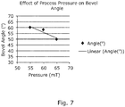
- Figure 9 shows the effect of changing the bevel angle from 57° to 75° on microneedle width. It can be seen that there is a 2.5 x reduction in the diameter of the microneedle if the bevel angle is increased from 57° to 75°.for a fixed bevel length This is a key factor in the production of high density silicon microneedle arrays. 57° corresponds to the bevel angle produced using wet etch techniques. This bevel angle is set owing to the crystallographic nature of the wet etch. Consequently, the prior art wet etch technique places a fundamental constraint on the design of the microneedle array. The present invention overcomes this limitation in the prior art.
- a further advantage of the dry etch method provided by the invention is that there is a substantial reduction in process time compared to a standard KOH wet etch. Typical process times for a dry etch of the invention are around 20 minutes to produce microneedles of 400 micron length. In contrast, a KOH wet etch would take about 22 hours microneedles of the same length. Additionally, the dry etch method of the invention avoids problems associated with roughness that are caused by a wet etch technique.
- the present invention can produce profile angles of 50° -80° and etch feature depths of 150-400 microns. However, the invention is not limited to these angles and depths.
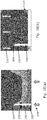
- Figures 10A and B are annotated SEMs depicting further stages in the production of the microneedles.
- Figure 10A shows the silicon substrate 106 after exposure to the backside plasma etch 100.
- a second mask 104 is positioned on a sloping sidewall partially to act as an etch stop for the backside plasma etch.
- the third mask 104 is positioned on the rear face of the silicon substrate 104 and is patterned to expose portions of the silicon to the backside plasma etch in order to form bore channels 108.
- the masks 102, 104 are aligned to ensure that the etching of the bore channel 108 stops at the second mask 104.
- FIG. 10B shows the subsequent plasma etch of the front face of the silicon substrate using a DRIE plasma etch 110.
- the second mask 104 protects the silicon underneath it from the plasma 110 whilst bulk silicon is removed by the plasma 110 in unmasked areas.
- the plasma 110 is substantially anisotropic in nature, resulting in the formation of a hollow, bevelled microneedle 112.
- the plasma 110 also produces a ridge 114.
- the ridge 114 is associated with the sloping face of the etch feature which is opposite to the sloping face which produces the microneedle 112.
- the second and, optionally, the third masks can be removed using known means.
- a PE-CVD oxide is used to form a hard second mask 104.
- alternative materials such as a photo resist or a metal mask could be used instead.
- the third mask 102 may also be formed from a hard mask, photo resist or metal mask. Conveniently, the second and third masks are formed form the same material.
- the front side plasma etch which forms the microneedles is a DRIE plasma etch.
- a typical cyclical etch and deposition process can be used with ICP HF source powers 3-6kW, bias power 0.12 - 1.5kW, process pressures 40-50mT, cycle time 1-5seconds and principally SF 6 during the etch cycle and C 4 F 8 during the deposition cycle.
- the front side plasma etch is desirably substantially anisotropic, and in fact it is possible to produce microneedles with completely vertical upstanding walls. However, it is generally preferred to provide microneedles having a re-entrant shape (wider top, narrower base) because the plasma etch processes which create re-entrant angles are typically less polymeric in nature, and hence more repeatable and robust.
- the backside plasma etch may be of the same type as the front face plasma etch which is used to produce the microneedles. In some embodiments, the same etch process is used for both the backside and front face etches.
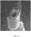
- the front face plasma etch can be used to obtain single or double bevelled microneedle tips. It has been found that if a relatively thick oxide second mask having a thickness of greater than 5 microns is used, then a single bevel structure can be obtained as can be seen in Figure 11 As noted previously, a double bevelled microneedle tip can be obtained through appropriate control of the SF 6 based first etch. It has been found that double bevel tips can also be obtained through control of the front face etch of the silicon substrate which produces the microneedles. Due the higher incidents of energetic ions, the etch rate of the second mask at the bottom of the bevelled structure is much higher than at the top.
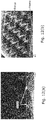
- Figures 12A and B show SEM images of double bevelled microneedles in which the top bevel angle is about 60° and the bottom bevel angle is steeper at about 80°. Microneedles having bevelled tips of a diamond shape result in the most effective skin puncture. The microneedles shown in Figure 12A and B have the desired diamond shaped tips, and in fact microneedles with diamond shaped tips can be readily produced using the present invention.
- the ridges can form a plurality of fence structures which surround the microneedles. This can be seen particularly clearly in Figure 12B .
- the perimeter of the silicon substrate which was masked by the first mask forms a frame structure which surrounds the array of microneedles.
- the ridges are typically formed at a distance of 100-200 microns from the base of the adjacent microneedles. However, smaller or greater distances can be utilised, primarily through appropriate design of the first mask but also through control of the etch processes.
- the presence of the ridges/frame structures is advantageous for a number of reasons.
- the likelihood of breakage of the microneedles (which is primarily caused by shear forces during injection of the microneedles into the skin) is reduced.
- the ridge/fence structures also allow stretching and bunching of the skin area local to the microneedles to give better skin penetration.
- Another advantage is that the ridge/fence structures can be used to define the microneedle penetration depth.
- the positioning of the microneedle shaft alongside the ridge/fence structures defines a needle penetration depth which is related to the difference between the microneedle height and the ridge height. This enables target drug delivery depth to be achieved.
- microneedles are produced.
- solid microneedles might be manufactured by omitting the backside etch step.
- pocketed microneedles might be produced having pockets or cavities formed either in the tip or in the microneedle body.
- the microneedles exemplified above have a cylindrical body shape, it is possible to instead produce microneedles having non-cylindrical body shapes of various forms.
Landscapes
- Health & Medical Sciences (AREA)
- Engineering & Computer Science (AREA)
- Dermatology (AREA)
- Manufacturing & Machinery (AREA)
- Life Sciences & Earth Sciences (AREA)
- Veterinary Medicine (AREA)
- Public Health (AREA)
- General Health & Medical Sciences (AREA)
- Animal Behavior & Ethology (AREA)
- Chemical & Material Sciences (AREA)
- Heart & Thoracic Surgery (AREA)
- Hematology (AREA)
- Biomedical Technology (AREA)
- Anesthesiology (AREA)
- Medical Informatics (AREA)
- Microelectronics & Electronic Packaging (AREA)
- Analytical Chemistry (AREA)
- Medicinal Chemistry (AREA)
- Pharmacology & Pharmacy (AREA)
- Epidemiology (AREA)
- Drying Of Semiconductors (AREA)
- Micromachines (AREA)
- Media Introduction/Drainage Providing Device (AREA)
- Materials For Medical Uses (AREA)
- Physics & Mathematics (AREA)
- Plasma & Fusion (AREA)
Claims (15)
- Verfahren zur Herstellung mehrerer Siliciummikronadeln, die eine abgeschrägte Spitze haben, wobei das Verfahren die folgenden Schritte beinhaltet:Bereitstellen eines Siliciumsubstrats (12) mit einer Frontfläche und einer Rückfläche;Bilden einer ersten Maskenanordnung (10) auf der Frontfläche des Substrats, wobei die erste Maskenanordnung eine oder mehrere Lücken (14) definiert;Durchführen einer SF6-basierten Plasmaätzung (15) der Frontfläche durch die Lücken in der ersten Maskenanordnung, um ein oder mehrere Ätzmerkmale mit einer geneigten Fläche bereitzustellen, wobei die SF6-basierte Plasmaätzung die erste Maskenanordnung mit einem Hinterschnitt unterätzt, die wenigstens 10 % der Tiefe eines entsprechenden Ätzmerkmals ausmacht;Bilden einer zweiten Maskenanordnung (18) auf den Ätzmerkmalen, um Stellen der Mikronadeln zu definieren, in denen sich die zweite Maskenanordnung gänzlich auf geneigten Flächen der Ätzmerkmale befinden; undDurchführen einer anisotropen DRIE-(Deep Reactive Ion Etch)-Plasmaätzung (24) auf der geätzten Frontfläche des Substrats, um mehrere Mikronadeln zu bilden, die eine abgeschrägte Spitze haben, wobei die geneigten Flächen der Ätzmerkmale die abgeschrägten Spitzen der Mikronadeln wenigstens teilweise entstehen lassen.
- Verfahren nach Anspruch 1, bei dem die SF6-basierte Plasmaätzung in einem gasförmigen Gemisch gebildet wird, das SF6 und einen Seitenwandpassivierungsvorläufer umfasst.
- Verfahren nach Anspruch 2, bei dem der Seitenwandpassivierungsvorläufer C4F8 und/oder CHF3 ist.
- Verfahren nach Anspruch 3, bei dem das gasförmige Gemisch im Wesentlichen aus SF6, CHF3 und C4F8 besteht.
- Verfahren nach einem der Ansprüche 2 bis 4, bei dem das gasförmige Gemisch ferner O2 umfasst.
- Verfahren nach Anspruch 5, bei dem das gasförmige Gemisch im Wesentlichen aus SF6, O2 und C4F8 besteht.
- Verfahren nach einem vorherigen Anspruch, bei dem die SF6-basierte Plasmaätzung in einem gasförmigen Gemisch gebildet wird, das SF6 und ein inertes Verdünnungsmittel umfasst.
- Verfahren nach Anspruch 7, bei dem das gasförmige Gemisch im Wesentlichen aus SF6, O2, C4F8 und Ar besteht.
- Verfahren nach einem vorherigen Anspruch, bei dem die DRIE-Plasmaätzung der geätzten Frontfläche ein anisotroper zyklischer Ätz- und Absetzprozess ist.
- Verfahren nach einem vorherigen Anspruch, das ferner den Schritt des Durchführens einer DRIE-Plasmaätzung der Rückseite umfasst, um mehrere Kanäle in dem Siliciumsubstrat auszubilden, die so positioniert sind, dass nach dem Bilden der mehreren Mikronadeln die Kanäle als Bohrungsdurchgänge dienen, die durch die Mikronadeln verlaufen.
- Verfahren nach einem vorherigen Anspruch, bei dem die abgeschrägten Spitzen der Mikronadeln als einzeln abgeschrägte Strukturen oder als doppelt abgeschrägte Strukturen ausgebildet sind.
- Verfahren nach Anspruch 11, bei dem doppelt abgeschrägte Strukturen durch Steuern von Ätzbedingungen während des Schritts des Durchführens einer SF6-basierten Plasmaätzung der Frontfläche ausgebildet sind, oder der Schritt des Durchführens einer SF6-basierten Plasmaätzung der Frontfläche einzeln abgeschrägte Strukturen produziert und doppelt abgeschrägte Strukturen während des Schrittes des Durchführens einer DRIE-Plasmaätzung der geätzten Frontfläche produziert werden.
- Verfahren nach einem vorherigen Anspruch, bei dem die DRIE-Plasmaätzung der geätzten Frontfläche eine oder mehrere Gratstrukturen bildet, die von den Mikronadeln beabstandet sind.
- Verfahren nach Anspruch 13, bei dem mehrere verbundene Gratstrukturen ausgebildet sind, um mehrere Mikronadeln umgebende Zaunstrukturen bereitzustellen, die jeweils eine Mikronadel umgeben und von ihr beabstandet sind.
- Verfahren nach Anspruch 13 oder Anspruch 14, bei dem:die SF6-basierte Plasmaätzung durch eine Lücke in der ersten Maskenanordnung ätzt, um ein oder mehrere Ätzmerkmale bereitzustellen, die ein Paar gegenüberliegende geneigte Flächen haben, unddie DRIE-Plasmaätzung der geätzten Frontfläche so durchgeführt wird, dass eine aus dem Paar gegenüberliegender geneigter Flächen wenigstens teilweise die abgeschrägte Spitze einer Mikronadel entstehen lässt und die andere aus dem Paar gegenüberliegender geneigter Flächen wenigstens teilweise einen von der Mikronadel beabstandeten Grad entstehen lässt.
Applications Claiming Priority (1)
| Application Number | Priority Date | Filing Date | Title |
|---|---|---|---|
| GBGB1709668.6A GB201709668D0 (en) | 2017-06-16 | 2017-06-16 | Microneedles |
Publications (2)
| Publication Number | Publication Date |
|---|---|
| EP3415465A1 EP3415465A1 (de) | 2018-12-19 |
| EP3415465B1 true EP3415465B1 (de) | 2020-08-05 |
Family
ID=59462460
Family Applications (1)
| Application Number | Title | Priority Date | Filing Date |
|---|---|---|---|
| EP18177390.4A Active EP3415465B1 (de) | 2017-06-16 | 2018-06-12 | Mikronadeln |
Country Status (5)
| Country | Link |
|---|---|
| US (1) | US10899606B2 (de) |
| EP (1) | EP3415465B1 (de) |
| JP (1) | JP7046728B2 (de) |
| KR (1) | KR20180137425A (de) |
| GB (1) | GB201709668D0 (de) |
Families Citing this family (6)
| Publication number | Priority date | Publication date | Assignee | Title |
|---|---|---|---|---|
| US20190366068A1 (en) * | 2018-05-29 | 2019-12-05 | Zibo Tanwei Nanotechnology Co., Ltd. | Microneedle for biosensing and method of fabrication |
| CN109795978A (zh) * | 2018-12-26 | 2019-05-24 | 华中科技大学 | 一种微型空心硅针管阵列及其制作方法 |
| EP3772331A1 (de) * | 2019-08-08 | 2021-02-10 | PKvitality | Körperüberwachungssystem mit einer mikronadel |
| CN110812686B (zh) * | 2019-11-07 | 2021-07-30 | 河南大学 | 一种制造微针阵列的微加工工艺和微针 |
| FR3107962B1 (fr) * | 2020-03-09 | 2022-03-04 | Vmicro | Dispositif de détection pour microscope à sonde locale |
| EP4202979A1 (de) | 2021-12-22 | 2023-06-28 | SPTS Technologies Limited | Verfahren zur verminderung der oberflächenrauheit |
Family Cites Families (17)
| Publication number | Priority date | Publication date | Assignee | Title |
|---|---|---|---|---|
| DE4241045C1 (de) | 1992-12-05 | 1994-05-26 | Bosch Gmbh Robert | Verfahren zum anisotropen Ätzen von Silicium |
| US6503231B1 (en) * | 1998-06-10 | 2003-01-07 | Georgia Tech Research Corporation | Microneedle device for transport of molecules across tissue |
| DE10024883A1 (de) | 2000-05-19 | 2001-11-29 | Bosch Gmbh Robert | Plasmaätzanlage |
| US6962772B2 (en) * | 2002-12-27 | 2005-11-08 | Industrial Technology Research Inst. | Method for manufacturing 3-D high aspect-ratio microneedle array device |
| EP1962679B1 (de) * | 2005-12-14 | 2012-04-11 | Silex Microsystems AB | Verfahren zur herstellung von mikronadeln und seine anwendungen |
| TW200744534A (en) * | 2006-06-09 | 2007-12-16 | Univ Nat Chiao Tung | Microprobe array structure and manufacturing method thereof |
| WO2008004597A1 (en) * | 2006-07-04 | 2008-01-10 | Toppan Printing Co., Ltd. | Method for manufacturing microneedle |
| EP2062611A4 (de) | 2006-08-18 | 2010-01-06 | Toppan Printing Co Ltd | Mikronadel und mikronadelstelle |
| MY157968A (en) | 2007-11-14 | 2016-08-30 | Mimos Berhad | Method for fabricating microneedled and microneedle fabricated from the same |
| EP2072076A1 (de) * | 2007-12-17 | 2009-06-24 | Debiotech S.A. | Herstellungsverfahren für Mikronadeln für den Außenbereich eines Flugzeugs |
| WO2009097660A1 (en) * | 2008-02-07 | 2009-08-13 | The University Of Queensland | Patch production |
| CN101244303B (zh) * | 2008-02-22 | 2010-09-01 | 清华大学 | 微型实心或空心硅针、硅针阵列及其制造方法 |
| FI20095433A0 (fi) * | 2009-04-20 | 2009-04-20 | Valtion Teknillinen | Mikroneula |
| EP4218891A1 (de) * | 2010-10-19 | 2023-08-02 | Trustees Of Tufts College | Mikronadeln auf seidenfibroinbasis und verfahren zur herstellung davon |
| US8133349B1 (en) | 2010-11-03 | 2012-03-13 | Lam Research Corporation | Rapid and uniform gas switching for a plasma etch process |
| SE538018C2 (sv) * | 2011-12-22 | 2016-02-09 | Silex Microsystems Ab | Isolering av mikrostrukturer |
| GB201318700D0 (en) | 2013-10-23 | 2013-12-04 | Univ Swansea | Manufacture of microneedles |
-
2017
- 2017-06-16 GB GBGB1709668.6A patent/GB201709668D0/en not_active Ceased
-
2018
- 2018-06-12 EP EP18177390.4A patent/EP3415465B1/de active Active
- 2018-06-15 US US16/010,395 patent/US10899606B2/en active Active
- 2018-06-15 KR KR1020180069055A patent/KR20180137425A/ko not_active Withdrawn
- 2018-06-15 JP JP2018114224A patent/JP7046728B2/ja active Active
Non-Patent Citations (1)
| Title |
|---|
| None * |
Also Published As
| Publication number | Publication date |
|---|---|
| GB201709668D0 (en) | 2017-08-02 |
| EP3415465A1 (de) | 2018-12-19 |
| US10899606B2 (en) | 2021-01-26 |
| JP7046728B2 (ja) | 2022-04-04 |
| JP2019000646A (ja) | 2019-01-10 |
| US20180362334A1 (en) | 2018-12-20 |
| KR20180137425A (ko) | 2018-12-27 |
Similar Documents
| Publication | Publication Date | Title |
|---|---|---|
| US10899606B2 (en) | Microneedles | |
| EP1244495B1 (de) | Verfahren zur herstellung vertikaler hohlnadeln aus einem halbleitersubstrat | |
| US8137736B2 (en) | Fabrication method for hollow microneedles for drug delivery | |
| US8354033B2 (en) | Method for producing porous microneedles and their use | |
| EP2036586B1 (de) | Verfahren zur herstellung einer mikronadel | |
| CA2749347C (en) | Patch production | |
| CN100540086C (zh) | 用来制造侧开口微型针的方法及模具 | |
| JP3696513B2 (ja) | 針状体の製造方法 | |
| JP4457229B2 (ja) | マイクロニードルおよびマイクロニードルの製造 | |
| US9919916B2 (en) | Manufacture of microneedles | |
| US10918844B2 (en) | Needle-like structure and method for manufacturing the same | |
| KR20060089314A (ko) | 마이크로 니들 어레이 제조방법 | |
| Wilke et al. | Silicon microneedle formation using modified mask designs based on convex corner undercut | |
| KR101622388B1 (ko) | 실리콘 마이크로 니들 스탬프 및 그 제조방법 | |
| JP4486368B2 (ja) | シリコン針の製造方法 | |
| EP4124355A1 (de) | Silizium-mikronadelstruktur und produktionsverfahren | |
| JP2004058265A (ja) | 針状構造体の作製方法 | |
| US9526885B1 (en) | Microneedles with sharpened tips and corresponding method of fabrication | |
| KR20190099612A (ko) | 마이크로 니들 어레이 및 마이크로 니들 어레이 제조 방법 |
Legal Events
| Date | Code | Title | Description |
|---|---|---|---|
| PUAI | Public reference made under article 153(3) epc to a published international application that has entered the european phase |
Free format text: ORIGINAL CODE: 0009012 |
|
| STAA | Information on the status of an ep patent application or granted ep patent |
Free format text: STATUS: THE APPLICATION HAS BEEN PUBLISHED |
|
| AK | Designated contracting states |
Kind code of ref document: A1 Designated state(s): AL AT BE BG CH CY CZ DE DK EE ES FI FR GB GR HR HU IE IS IT LI LT LU LV MC MK MT NL NO PL PT RO RS SE SI SK SM TR |
|
| AX | Request for extension of the european patent |
Extension state: BA ME |
|
| STAA | Information on the status of an ep patent application or granted ep patent |
Free format text: STATUS: REQUEST FOR EXAMINATION WAS MADE |
|
| 17P | Request for examination filed |
Effective date: 20190528 |
|
| RBV | Designated contracting states (corrected) |
Designated state(s): AL AT BE BG CH CY CZ DE DK EE ES FI FR GB GR HR HU IE IS IT LI LT LU LV MC MK MT NL NO PL PT RO RS SE SI SK SM TR |
|
| GRAP | Despatch of communication of intention to grant a patent |
Free format text: ORIGINAL CODE: EPIDOSNIGR1 |
|
| STAA | Information on the status of an ep patent application or granted ep patent |
Free format text: STATUS: GRANT OF PATENT IS INTENDED |
|
| RIC1 | Information provided on ipc code assigned before grant |
Ipc: A61M 37/00 20060101ALI20200219BHEP Ipc: B81C 1/00 20060101AFI20200219BHEP |
|
| INTG | Intention to grant announced |
Effective date: 20200319 |
|
| GRAS | Grant fee paid |
Free format text: ORIGINAL CODE: EPIDOSNIGR3 |
|
| RIN1 | Information on inventor provided before grant (corrected) |
Inventor name: ASHRAF, HUMA Inventor name: ENG, PEY FEN Inventor name: ROBERTS, KERRY |
|
| GRAA | (expected) grant |
Free format text: ORIGINAL CODE: 0009210 |
|
| STAA | Information on the status of an ep patent application or granted ep patent |
Free format text: STATUS: THE PATENT HAS BEEN GRANTED |
|
| AK | Designated contracting states |
Kind code of ref document: B1 Designated state(s): AL AT BE BG CH CY CZ DE DK EE ES FI FR GB GR HR HU IE IS IT LI LT LU LV MC MK MT NL NO PL PT RO RS SE SI SK SM TR |
|
| REG | Reference to a national code |
Ref country code: GB Ref legal event code: FG4D |
|
| REG | Reference to a national code |
Ref country code: CH Ref legal event code: EP |
|
| REG | Reference to a national code |
Ref country code: AT Ref legal event code: REF Ref document number: 1298464 Country of ref document: AT Kind code of ref document: T Effective date: 20200815 |
|
| REG | Reference to a national code |
Ref country code: DE Ref legal event code: R096 Ref document number: 602018006580 Country of ref document: DE |
|
| REG | Reference to a national code |
Ref country code: IE Ref legal event code: FG4D |
|
| REG | Reference to a national code |
Ref country code: LT Ref legal event code: MG4D |
|
| REG | Reference to a national code |
Ref country code: NL Ref legal event code: MP Effective date: 20200805 |
|
| REG | Reference to a national code |
Ref country code: AT Ref legal event code: MK05 Ref document number: 1298464 Country of ref document: AT Kind code of ref document: T Effective date: 20200805 |
|
| PG25 | Lapsed in a contracting state [announced via postgrant information from national office to epo] |
Ref country code: AT Free format text: LAPSE BECAUSE OF FAILURE TO SUBMIT A TRANSLATION OF THE DESCRIPTION OR TO PAY THE FEE WITHIN THE PRESCRIBED TIME-LIMIT Effective date: 20200805 Ref country code: BG Free format text: LAPSE BECAUSE OF FAILURE TO SUBMIT A TRANSLATION OF THE DESCRIPTION OR TO PAY THE FEE WITHIN THE PRESCRIBED TIME-LIMIT Effective date: 20201105 Ref country code: HR Free format text: LAPSE BECAUSE OF FAILURE TO SUBMIT A TRANSLATION OF THE DESCRIPTION OR TO PAY THE FEE WITHIN THE PRESCRIBED TIME-LIMIT Effective date: 20200805 Ref country code: GR Free format text: LAPSE BECAUSE OF FAILURE TO SUBMIT A TRANSLATION OF THE DESCRIPTION OR TO PAY THE FEE WITHIN THE PRESCRIBED TIME-LIMIT Effective date: 20201106 Ref country code: NO Free format text: LAPSE BECAUSE OF FAILURE TO SUBMIT A TRANSLATION OF THE DESCRIPTION OR TO PAY THE FEE WITHIN THE PRESCRIBED TIME-LIMIT Effective date: 20201105 Ref country code: LT Free format text: LAPSE BECAUSE OF FAILURE TO SUBMIT A TRANSLATION OF THE DESCRIPTION OR TO PAY THE FEE WITHIN THE PRESCRIBED TIME-LIMIT Effective date: 20200805 Ref country code: ES Free format text: LAPSE BECAUSE OF FAILURE TO SUBMIT A TRANSLATION OF THE DESCRIPTION OR TO PAY THE FEE WITHIN THE PRESCRIBED TIME-LIMIT Effective date: 20200805 Ref country code: PT Free format text: LAPSE BECAUSE OF FAILURE TO SUBMIT A TRANSLATION OF THE DESCRIPTION OR TO PAY THE FEE WITHIN THE PRESCRIBED TIME-LIMIT Effective date: 20201207 Ref country code: FI Free format text: LAPSE BECAUSE OF FAILURE TO SUBMIT A TRANSLATION OF THE DESCRIPTION OR TO PAY THE FEE WITHIN THE PRESCRIBED TIME-LIMIT Effective date: 20200805 Ref country code: SE Free format text: LAPSE BECAUSE OF FAILURE TO SUBMIT A TRANSLATION OF THE DESCRIPTION OR TO PAY THE FEE WITHIN THE PRESCRIBED TIME-LIMIT Effective date: 20200805 |
|
| PG25 | Lapsed in a contracting state [announced via postgrant information from national office to epo] |
Ref country code: RS Free format text: LAPSE BECAUSE OF FAILURE TO SUBMIT A TRANSLATION OF THE DESCRIPTION OR TO PAY THE FEE WITHIN THE PRESCRIBED TIME-LIMIT Effective date: 20200805 Ref country code: LV Free format text: LAPSE BECAUSE OF FAILURE TO SUBMIT A TRANSLATION OF THE DESCRIPTION OR TO PAY THE FEE WITHIN THE PRESCRIBED TIME-LIMIT Effective date: 20200805 Ref country code: PL Free format text: LAPSE BECAUSE OF FAILURE TO SUBMIT A TRANSLATION OF THE DESCRIPTION OR TO PAY THE FEE WITHIN THE PRESCRIBED TIME-LIMIT Effective date: 20200805 Ref country code: NL Free format text: LAPSE BECAUSE OF FAILURE TO SUBMIT A TRANSLATION OF THE DESCRIPTION OR TO PAY THE FEE WITHIN THE PRESCRIBED TIME-LIMIT Effective date: 20200805 Ref country code: IS Free format text: LAPSE BECAUSE OF FAILURE TO SUBMIT A TRANSLATION OF THE DESCRIPTION OR TO PAY THE FEE WITHIN THE PRESCRIBED TIME-LIMIT Effective date: 20201205 |
|
| PG25 | Lapsed in a contracting state [announced via postgrant information from national office to epo] |
Ref country code: EE Free format text: LAPSE BECAUSE OF FAILURE TO SUBMIT A TRANSLATION OF THE DESCRIPTION OR TO PAY THE FEE WITHIN THE PRESCRIBED TIME-LIMIT Effective date: 20200805 Ref country code: RO Free format text: LAPSE BECAUSE OF FAILURE TO SUBMIT A TRANSLATION OF THE DESCRIPTION OR TO PAY THE FEE WITHIN THE PRESCRIBED TIME-LIMIT Effective date: 20200805 Ref country code: DK Free format text: LAPSE BECAUSE OF FAILURE TO SUBMIT A TRANSLATION OF THE DESCRIPTION OR TO PAY THE FEE WITHIN THE PRESCRIBED TIME-LIMIT Effective date: 20200805 Ref country code: CZ Free format text: LAPSE BECAUSE OF FAILURE TO SUBMIT A TRANSLATION OF THE DESCRIPTION OR TO PAY THE FEE WITHIN THE PRESCRIBED TIME-LIMIT Effective date: 20200805 Ref country code: SM Free format text: LAPSE BECAUSE OF FAILURE TO SUBMIT A TRANSLATION OF THE DESCRIPTION OR TO PAY THE FEE WITHIN THE PRESCRIBED TIME-LIMIT Effective date: 20200805 |
|
| REG | Reference to a national code |
Ref country code: DE Ref legal event code: R097 Ref document number: 602018006580 Country of ref document: DE |
|
| PG25 | Lapsed in a contracting state [announced via postgrant information from national office to epo] |
Ref country code: AL Free format text: LAPSE BECAUSE OF FAILURE TO SUBMIT A TRANSLATION OF THE DESCRIPTION OR TO PAY THE FEE WITHIN THE PRESCRIBED TIME-LIMIT Effective date: 20200805 |
|
| PLBE | No opposition filed within time limit |
Free format text: ORIGINAL CODE: 0009261 |
|
| STAA | Information on the status of an ep patent application or granted ep patent |
Free format text: STATUS: NO OPPOSITION FILED WITHIN TIME LIMIT |
|
| PG25 | Lapsed in a contracting state [announced via postgrant information from national office to epo] |
Ref country code: SK Free format text: LAPSE BECAUSE OF FAILURE TO SUBMIT A TRANSLATION OF THE DESCRIPTION OR TO PAY THE FEE WITHIN THE PRESCRIBED TIME-LIMIT Effective date: 20200805 |
|
| 26N | No opposition filed |
Effective date: 20210507 |
|
| PG25 | Lapsed in a contracting state [announced via postgrant information from national office to epo] |
Ref country code: IT Free format text: LAPSE BECAUSE OF FAILURE TO SUBMIT A TRANSLATION OF THE DESCRIPTION OR TO PAY THE FEE WITHIN THE PRESCRIBED TIME-LIMIT Effective date: 20200805 |
|
| PG25 | Lapsed in a contracting state [announced via postgrant information from national office to epo] |
Ref country code: SI Free format text: LAPSE BECAUSE OF FAILURE TO SUBMIT A TRANSLATION OF THE DESCRIPTION OR TO PAY THE FEE WITHIN THE PRESCRIBED TIME-LIMIT Effective date: 20200805 |
|
| PG25 | Lapsed in a contracting state [announced via postgrant information from national office to epo] |
Ref country code: MC Free format text: LAPSE BECAUSE OF FAILURE TO SUBMIT A TRANSLATION OF THE DESCRIPTION OR TO PAY THE FEE WITHIN THE PRESCRIBED TIME-LIMIT Effective date: 20200805 |
|
| REG | Reference to a national code |
Ref country code: CH Ref legal event code: PL |
|
| REG | Reference to a national code |
Ref country code: BE Ref legal event code: MM Effective date: 20210630 |
|
| PG25 | Lapsed in a contracting state [announced via postgrant information from national office to epo] |
Ref country code: LU Free format text: LAPSE BECAUSE OF NON-PAYMENT OF DUE FEES Effective date: 20210612 |
|
| PG25 | Lapsed in a contracting state [announced via postgrant information from national office to epo] |
Ref country code: LI Free format text: LAPSE BECAUSE OF NON-PAYMENT OF DUE FEES Effective date: 20210630 Ref country code: IE Free format text: LAPSE BECAUSE OF NON-PAYMENT OF DUE FEES Effective date: 20210612 Ref country code: CH Free format text: LAPSE BECAUSE OF NON-PAYMENT OF DUE FEES Effective date: 20210630 |
|
| PG25 | Lapsed in a contracting state [announced via postgrant information from national office to epo] |
Ref country code: BE Free format text: LAPSE BECAUSE OF NON-PAYMENT OF DUE FEES Effective date: 20210630 |
|
| PG25 | Lapsed in a contracting state [announced via postgrant information from national office to epo] |
Ref country code: CY Free format text: LAPSE BECAUSE OF FAILURE TO SUBMIT A TRANSLATION OF THE DESCRIPTION OR TO PAY THE FEE WITHIN THE PRESCRIBED TIME-LIMIT Effective date: 20200805 |
|
| P01 | Opt-out of the competence of the unified patent court (upc) registered |
Effective date: 20230525 |
|
| PG25 | Lapsed in a contracting state [announced via postgrant information from national office to epo] |
Ref country code: HU Free format text: LAPSE BECAUSE OF FAILURE TO SUBMIT A TRANSLATION OF THE DESCRIPTION OR TO PAY THE FEE WITHIN THE PRESCRIBED TIME-LIMIT; INVALID AB INITIO Effective date: 20180612 |
|
| REG | Reference to a national code |
Ref country code: DE Ref legal event code: R082 Ref document number: 602018006580 Country of ref document: DE Representative=s name: KANDLBINDER, MARKUS, DIPL.-PHYS., DE |
|
| PG25 | Lapsed in a contracting state [announced via postgrant information from national office to epo] |
Ref country code: MK Free format text: LAPSE BECAUSE OF FAILURE TO SUBMIT A TRANSLATION OF THE DESCRIPTION OR TO PAY THE FEE WITHIN THE PRESCRIBED TIME-LIMIT Effective date: 20200805 |
|
| PG25 | Lapsed in a contracting state [announced via postgrant information from national office to epo] |
Ref country code: TR Free format text: LAPSE BECAUSE OF FAILURE TO SUBMIT A TRANSLATION OF THE DESCRIPTION OR TO PAY THE FEE WITHIN THE PRESCRIBED TIME-LIMIT Effective date: 20200805 |
|
| PG25 | Lapsed in a contracting state [announced via postgrant information from national office to epo] |
Ref country code: MT Free format text: LAPSE BECAUSE OF FAILURE TO SUBMIT A TRANSLATION OF THE DESCRIPTION OR TO PAY THE FEE WITHIN THE PRESCRIBED TIME-LIMIT Effective date: 20200805 |
|
| PGFP | Annual fee paid to national office [announced via postgrant information from national office to epo] |
Ref country code: DE Payment date: 20250627 Year of fee payment: 8 |
|
| PGFP | Annual fee paid to national office [announced via postgrant information from national office to epo] |
Ref country code: GB Payment date: 20250627 Year of fee payment: 8 |
|
| PGFP | Annual fee paid to national office [announced via postgrant information from national office to epo] |
Ref country code: FR Payment date: 20250625 Year of fee payment: 8 |