EP3414819B1 - Module de convertisseur pour une centrale de transmission à haute tension à courant continu - Google Patents
Module de convertisseur pour une centrale de transmission à haute tension à courant continu Download PDFInfo
- Publication number
- EP3414819B1 EP3414819B1 EP16703993.2A EP16703993A EP3414819B1 EP 3414819 B1 EP3414819 B1 EP 3414819B1 EP 16703993 A EP16703993 A EP 16703993A EP 3414819 B1 EP3414819 B1 EP 3414819B1
- Authority
- EP
- European Patent Office
- Prior art keywords
- switching
- module
- node
- converter
- converter module
- Prior art date
- Legal status (The legal status is an assumption and is not a legal conclusion. Google has not performed a legal analysis and makes no representation as to the accuracy of the status listed.)
- Active
Links
- 239000003990 capacitor Substances 0.000 claims description 100
- 238000001514 detection method Methods 0.000 claims description 10
- 239000004065 semiconductor Substances 0.000 claims description 9
- 230000004913 activation Effects 0.000 claims description 4
- 230000005540 biological transmission Effects 0.000 claims description 4
- 230000009849 deactivation Effects 0.000 claims description 3
- 230000005669 field effect Effects 0.000 claims description 3
- 125000005842 heteroatom Chemical group 0.000 claims description 3
- 238000010586 diagram Methods 0.000 description 11
- 238000004146 energy storage Methods 0.000 description 7
- 230000001960 triggered effect Effects 0.000 description 3
- 230000009286 beneficial effect Effects 0.000 description 2
- JBRZTFJDHDCESZ-UHFFFAOYSA-N AsGa Chemical compound [As]#[Ga] JBRZTFJDHDCESZ-UHFFFAOYSA-N 0.000 description 1
- 229910002601 GaN Inorganic materials 0.000 description 1
- 229910001218 Gallium arsenide Inorganic materials 0.000 description 1
- JMASRVWKEDWRBT-UHFFFAOYSA-N Gallium nitride Chemical compound [Ga]#N JMASRVWKEDWRBT-UHFFFAOYSA-N 0.000 description 1
- XUIMIQQOPSSXEZ-UHFFFAOYSA-N Silicon Chemical compound [Si] XUIMIQQOPSSXEZ-UHFFFAOYSA-N 0.000 description 1
- 230000001419 dependent effect Effects 0.000 description 1
- 230000005672 electromagnetic field Effects 0.000 description 1
- 238000005516 engineering process Methods 0.000 description 1
- 238000004519 manufacturing process Methods 0.000 description 1
- 239000000463 material Substances 0.000 description 1
- 238000000034 method Methods 0.000 description 1
- 230000003071 parasitic effect Effects 0.000 description 1
- 229910052710 silicon Inorganic materials 0.000 description 1
- 239000010703 silicon Substances 0.000 description 1
- HBMJWWWQQXIZIP-UHFFFAOYSA-N silicon carbide Chemical compound [Si+]#[C-] HBMJWWWQQXIZIP-UHFFFAOYSA-N 0.000 description 1
- 229910010271 silicon carbide Inorganic materials 0.000 description 1
- 230000003068 static effect Effects 0.000 description 1
- 230000001360 synchronised effect Effects 0.000 description 1
Images


Classifications
-
- H—ELECTRICITY
- H02—GENERATION; CONVERSION OR DISTRIBUTION OF ELECTRIC POWER
- H02M—APPARATUS FOR CONVERSION BETWEEN AC AND AC, BETWEEN AC AND DC, OR BETWEEN DC AND DC, AND FOR USE WITH MAINS OR SIMILAR POWER SUPPLY SYSTEMS; CONVERSION OF DC OR AC INPUT POWER INTO SURGE OUTPUT POWER; CONTROL OR REGULATION THEREOF
- H02M1/00—Details of apparatus for conversion
- H02M1/32—Means for protecting converters other than automatic disconnection
-
- H—ELECTRICITY
- H02—GENERATION; CONVERSION OR DISTRIBUTION OF ELECTRIC POWER
- H02H—EMERGENCY PROTECTIVE CIRCUIT ARRANGEMENTS
- H02H7/00—Emergency protective circuit arrangements specially adapted for specific types of electric machines or apparatus or for sectionalised protection of cable or line systems, and effecting automatic switching in the event of an undesired change from normal working conditions
- H02H7/10—Emergency protective circuit arrangements specially adapted for specific types of electric machines or apparatus or for sectionalised protection of cable or line systems, and effecting automatic switching in the event of an undesired change from normal working conditions for converters; for rectifiers
- H02H7/12—Emergency protective circuit arrangements specially adapted for specific types of electric machines or apparatus or for sectionalised protection of cable or line systems, and effecting automatic switching in the event of an undesired change from normal working conditions for converters; for rectifiers for static converters or rectifiers
- H02H7/122—Emergency protective circuit arrangements specially adapted for specific types of electric machines or apparatus or for sectionalised protection of cable or line systems, and effecting automatic switching in the event of an undesired change from normal working conditions for converters; for rectifiers for static converters or rectifiers for inverters, i.e. dc/ac converters
- H02H7/1225—Emergency protective circuit arrangements specially adapted for specific types of electric machines or apparatus or for sectionalised protection of cable or line systems, and effecting automatic switching in the event of an undesired change from normal working conditions for converters; for rectifiers for static converters or rectifiers for inverters, i.e. dc/ac converters responsive to internal faults, e.g. shoot-through
-
- H—ELECTRICITY
- H02—GENERATION; CONVERSION OR DISTRIBUTION OF ELECTRIC POWER
- H02M—APPARATUS FOR CONVERSION BETWEEN AC AND AC, BETWEEN AC AND DC, OR BETWEEN DC AND DC, AND FOR USE WITH MAINS OR SIMILAR POWER SUPPLY SYSTEMS; CONVERSION OF DC OR AC INPUT POWER INTO SURGE OUTPUT POWER; CONTROL OR REGULATION THEREOF
- H02M5/00—Conversion of ac power input into ac power output, e.g. for change of voltage, for change of frequency, for change of number of phases
- H02M5/40—Conversion of ac power input into ac power output, e.g. for change of voltage, for change of frequency, for change of number of phases with intermediate conversion into dc
- H02M5/42—Conversion of ac power input into ac power output, e.g. for change of voltage, for change of frequency, for change of number of phases with intermediate conversion into dc by static converters
- H02M5/44—Conversion of ac power input into ac power output, e.g. for change of voltage, for change of frequency, for change of number of phases with intermediate conversion into dc by static converters using discharge tubes or semiconductor devices to convert the intermediate dc into ac
- H02M5/453—Conversion of ac power input into ac power output, e.g. for change of voltage, for change of frequency, for change of number of phases with intermediate conversion into dc by static converters using discharge tubes or semiconductor devices to convert the intermediate dc into ac using devices of a triode or transistor type requiring continuous application of a control signal
- H02M5/458—Conversion of ac power input into ac power output, e.g. for change of voltage, for change of frequency, for change of number of phases with intermediate conversion into dc by static converters using discharge tubes or semiconductor devices to convert the intermediate dc into ac using devices of a triode or transistor type requiring continuous application of a control signal using semiconductor devices only
- H02M5/4585—Conversion of ac power input into ac power output, e.g. for change of voltage, for change of frequency, for change of number of phases with intermediate conversion into dc by static converters using discharge tubes or semiconductor devices to convert the intermediate dc into ac using devices of a triode or transistor type requiring continuous application of a control signal using semiconductor devices only having a rectifier with controlled elements
-
- H—ELECTRICITY
- H02—GENERATION; CONVERSION OR DISTRIBUTION OF ELECTRIC POWER
- H02M—APPARATUS FOR CONVERSION BETWEEN AC AND AC, BETWEEN AC AND DC, OR BETWEEN DC AND DC, AND FOR USE WITH MAINS OR SIMILAR POWER SUPPLY SYSTEMS; CONVERSION OF DC OR AC INPUT POWER INTO SURGE OUTPUT POWER; CONTROL OR REGULATION THEREOF
- H02M7/00—Conversion of ac power input into dc power output; Conversion of dc power input into ac power output
- H02M7/42—Conversion of dc power input into ac power output without possibility of reversal
- H02M7/44—Conversion of dc power input into ac power output without possibility of reversal by static converters
- H02M7/48—Conversion of dc power input into ac power output without possibility of reversal by static converters using discharge tubes with control electrode or semiconductor devices with control electrode
- H02M7/483—Converters with outputs that each can have more than two voltages levels
- H02M7/4835—Converters with outputs that each can have more than two voltages levels comprising two or more cells, each including a switchable capacitor, the capacitors having a nominal charge voltage which corresponds to a given fraction of the input voltage, and the capacitors being selectively connected in series to determine the instantaneous output voltage
-
- H—ELECTRICITY
- H02—GENERATION; CONVERSION OR DISTRIBUTION OF ELECTRIC POWER
- H02M—APPARATUS FOR CONVERSION BETWEEN AC AND AC, BETWEEN AC AND DC, OR BETWEEN DC AND DC, AND FOR USE WITH MAINS OR SIMILAR POWER SUPPLY SYSTEMS; CONVERSION OF DC OR AC INPUT POWER INTO SURGE OUTPUT POWER; CONTROL OR REGULATION THEREOF
- H02M1/00—Details of apparatus for conversion
- H02M1/32—Means for protecting converters other than automatic disconnection
- H02M1/325—Means for protecting converters other than automatic disconnection with means for allowing continuous operation despite a fault, i.e. fault tolerant converters
Definitions
- the present disclosure relates to the field of converter modules.
- the present disclosure relates to the field of converter modules for high voltage direct current (HVDC) power station.
- HVDC high voltage direct current
- Power converter stations may comprise a valve unit formed of a stack (or column) of power converter modules.
- the converter modules may be connected in series.
- transistors or switches
- IGBT insulated-gate bipolar transistors
- the valve unit may also include a by-pass switch which, if a failure is detected at a converter module (such as for instance at one of the transistors of the converter module), provides another current path.
- a control unit may cause the converter module to be by-passed (short-circuited).
- the by-pass switch When the by-pass switch has been triggered, the energy stored in the capacitor of the converter module is totally discharged through the (closed or activated) by-pass switch or the failed transistor, which may create a very high current peak (in the range of for example hundreds of kilo amperes).
- An object of the present disclosure is therefore to at least partially overcome the challenge mentioned above.
- the present disclosure relates to embodiments in which the amount of energy being discharged upon failure of a transistor (or switching device) of the converter module is reduced.
- the converter module includes at least two switching modules connected in series and one of the two switching modules includes at least two switching devices.
- the power converter may include at least two capacitor units such that each of the two switching devices is electrically connected to one of the capacitor units.
- the capacitor or energy storage of the converter module may include at least two capacitor units. Embodiments with more than two capacitor units may be envisaged.
- a by-pass switch of the power converter may be activated (or triggered) such that the converter module will be by passed by the by-pass switch. Consequently the energy stored in the capacitor unit electrically connected to the failed switching device will be discharged.
- a first current path is provided for discharge of a first capacitor unit electrically connected to a first switching device upon failure of such first switching device and a second separate current path is provided for discharge of a second capacitor unit electrically connected to a second switching device upon failure of such second switching device.
- the discharge energy will be reduced by a factor of two, and the current peak may be reduced as a result.
- the converter module may be designed with more than two capacitor units and thus more than two current paths to discharge the energy stored to supply the transistors under operation. In these cases, the energy discharge may be further reduced by a factor greater than two, depending on the design.
- the embodiments of the present disclosure may alleviate at least some of the constraints on the by-pass switch that may be used in such HVDC power converter applications. For example, by limiting the current peak (i.e. reducing the energy discharge), a bypass switch that is smaller and cheaper to design and manufacture may be used.
- the embodiments of the present disclosure provide also for higher current rating for the converter module (or converter cell) and an improved scalability of converter module design for different power rating requirements.
- the embodiments of the present disclosure may use either a half bridge topology or full-bridge topology for the arrangement of the transistors (or switching modules/devices) forming the converter module (or converter cell).
- a converter module may include at least two switching modules connected in series via a node.
- the converter module may be equipped with a number of capacitor units to supply current to these switching modules and a number of independent current paths are provided for discharge of the capacitor units via a by-pass switch upon failure of any of transistors (or switches) of the switching modules.
- the converter module may include a first terminal for input of an (alternating) electrical current via a first connection line and a second terminal for output of the (alternating) electrical current via a second connection line. It will be appreciated that the first and second terminals may be interchangeable such that the second terminal may be used for input of the current to the converter module and the first terminal may be used for output of the current to the converter module. The principle remains the same.
- the converter module may include a by-pass switch connected between the first terminal and the second terminal.
- the converter module includes a first switching module and a second switching module connected in series via a first node connected to either one of the first terminal and the second terminal. At least the first switching module may include two switching devices and the second switching module may be connected between the first node and a second node.
- the converter module may also include at least two capacitor units, wherein a first capacitor unit is connected from the second node to a first switching device of the first switching module and a second capacitor unit is connected from the second node to a second switching device of the first switching module to form two separate current paths between the first node and the second node.
- the first switching module may include a plurality of switching devices and the converter module may comprise a plurality of capacitor units. Each of the capacitor units may be separately connected to one of the switching devices of the first switching module.
- a switching device of the first switching module may include a transistor having an emitter, a gate and a collector.
- the second switching module may be connected at the second node to either the emitters or the collectors of the switching devices of the first switching module.
- the gates of the switching devices of the first switching module are connected to a common control line or to separate control lines.
- the second switching module may include one or more switching device.
- a switching device may be one of an insulated-gate bipolar transistor (IGBT), a bi-mode insulated gate transistor (BIGT), a metal-oxide-semiconductor field-effect transistor (MOSFET), an integrated gate-commutated thyristor (IGCT), a gate turn-off thyristor (GTO), a high electron mobility transistor (HEMT) and a hetero junction bipolar transistor (HBT).
- IGBT insulated-gate bipolar transistor
- BIGT bi-mode insulated gate transistor
- MOSFET metal-oxide-semiconductor field-effect transistor
- IGCT integrated gate-commutated thyristor
- GTO gate turn-off thyristor
- HEMT high electron mobility transistor
- HBT hetero junction bipolar transistor
- the converter module may further comprise at least one resistive component.
- a first current path connecting the first capacitor unit to the first switching device of the first switching module may then be connected to a second current path connecting the second capacitor unit to the second switching device of the first switching module via such a resistive component.
- the resistive component may be a resistor, a surge arrestor, an inductor with a resistor, or the like.
- the resistive component may include at least two separate resistor elements (or resistive elements) connected in series at a node connected to the second node through at least a semiconductor switch or a mechanical switch.
- the by-pass switch may be connected in parallel with the second switching module between the first node and the second node.
- the second terminal may be connected to the second node.
- Such a connection of the by-pass switch is suitable for a half-bridge topology design.
- the converter module may further comprise a third switching module and a fourth switching module connected in series via a third node.
- the third switching module may include at least two switching devices and the fourth switching module may be connected between the second node and the third node.
- a first switching device of the third switching module is connected to the second node via the first capacitor unit and a second switching device of the third switching module is connected to the first node via the second capacitor unit to form two separate (or independent) current paths between the third node and the second node.
- the by-pass switch may be connected between the first node and the third node.
- a device comprising a control circuit and at least one converter module as defined in any one of the preceding embodiments.
- the control circuit may be configured to generate a signal (e.g. a control signal which may be an electrical signal) instructing at least one of (or all of) the switching devices of the converter module to turn off.
- control circuit may be further configured to instruct the by-pass switch to conduct current upon detection of the failure (for discharge of energy of the capacitor unit connected to the switching device at which the failure has been detected).
- control circuit may be configured to trigger the by-pass switch after a delay has elapsed since transmission of instructions to turn off (or deactivate) the switching devices of the converter module.
- control circuit may be configured to synchronize activation and deactivation of the switching devices of the converter module.
- a power converter station comprising a plurality of converter modules or devices as defined any one of the preceding embodiments.
- the plurality of converter modules may be connected in series and arranged as at least one column.
- the present disclosure also relates to all possible combinations of features mentioned herein. Any embodiment described herein may be combinable with other embodiments also described herein, and the present disclosure relates to all combinations of features.
- Figure 1 shows a circuit diagram illustrating the electrical arrangement of elements of a converter module 100 based on a half-bridge cell topology.
- the converter module 100 includes a first terminal 110 for input/output of an electrical (alternating) current to the converter module via a first connection line 112 and a second terminal 120 for output/input of the electrical (alternating) current from the converter module via a second connection line 122. It will be appreciated that the first and second terminals are arranged to provide input/output of a signal comprising both an AC component and a DC component.
- a by-pass switch 130 is connected between the first terminal 110 and the second terminal 120 such that, upon failure at the converter module, the by-pass switch may be activated (i.e. closed) and the current may be redirected to pass (or flow) through the by-pass switch.
- the converter module 100 further includes a first switching module 140 and a second switching module 150 connected in series via a first node 180.
- the first node 180 is connected to the first terminal 110.
- the first terminal 110 and the first node may therefore be considered to be at the same electrical potential level.
- the first switching module 140 includes two switching devices 142, 144 and the second switching module 150 is connected between the first node 180 and a second node 190.
- the first switching module includes two switching devices (or transistors) 142, 144 connected in parallel from the first node 180 and the second switching module 150 includes only one switching device (or transistor) 152.
- the second switching module 150 may include more than one switching device.
- the first and second switching modules may not only include a transistor but for instance also a diode.
- the converter module 100 includes also two capacitor units 160, 170.
- the two capacitor units may have the same voltage value (or at least similar capacitance values).
- the first capacitor unit 160 is connected from the second node 190 to the first switching device 142 of the first switching module 140 and the second capacitor unit 170 is connected from the second node 190 to the second switching device 144 of the first switching module 140 to form two separate current paths between the first node 180 and the second node 190.
- a first electrical current path, along which the first switching device 142 and the first capacitor unit 160 are connected in series, is electrically arranged in parallel with a second electrical current path along which the second switching device 144 and the second capacitor unit 170 are connected in series.
- the converter module of the present embodiment reduces the energy discharge upon failure of one of the switching devices of the converter module.
- the transistors (or switching devices)of the first and second switching modules may be insulated-gate bipolar transistors (IGBTs), bi-mode insulated gate transistors (BIGTs), metal-oxide-semiconductor field-effect transistor (MOSFETs), integrated gate-commutated thyristor (IGCTs), gate turn-off thyristors (GTOs), high electron mobility transistors (HEMTs) or hetero junction bipolar transistors (HBTs).
- IGBTs bi-mode insulated gate transistors
- MOSFETs metal-oxide-semiconductor field-effect transistor
- IGCTs integrated gate-commutated thyristor
- GTOs gate turn-off thyristors
- HEMTs high electron mobility transistors
- HBTs hetero junction bipolar transistors
- the switching device 142 of the first switching module 140 may include a transistor having an emitter 142a, a gate 142b and a collector 142c.
- the switching devices 142 and 144 of the first switching module 140 may for example be BIGTs or IGBTs.
- An IGBT 142 may comprise two semiconductor chips in the form of a transistor 142 and a diode 143 connected in parallel to the transistor 142, and a BIGT may be a single-chip component adapted to replace a two-chip IGBT, e.g. by integrating the functionality of the IGBT in a single semiconductor chip.
- a switching device in the form of a BIGT or IGBT, is illustrated in the circuit diagram in Figure 1 by a transistor 142 and a diode 143 electrically connected in parallel to the transistor 142, the diode 143 having a direction of conductance from an emitter 142c of the transistor 142 to a collector 142a of the transistor 142.
- the second switching device 144 of the first switching module 140 is illustrated by an IGBT or BIGT with a transistor and a diode electrically connected in parallel to the transistor, the diode having a direction of conductance from an emitter of the transistor to a collector of the transistor.
- a first electrode of the capacitor unit 160 is connected to the collector 142a of the transistor 142 and a second electrode of the capacitor unit 160 is connected to the second node 190.
- the second node 190 is connected to an emitter of the transistor 152 of the second switching module 150.
- one electrode of the first capacitor unit 160 is connected to the collector 142a of one of the two transistors of the first switching module 160 while its other electrode is connected to the emitter of the transistor 152 of the second switching module 170.
- a first electrode of the second capacitor unit 170 is connected to the collector of the second transistor (or second switching device) 144 while its second electrode is connected to the second node 190, i.e. the emitter of the transistor 152 of the second switching module 150.
- the second switching module 150 is connected at the first node 180 to the emitters of the switching devices of the first switching module 140.
- the second switching module is shown to include only one switching device (or transistor) in the present embodiment, other embodiments wherein the second switching module includes more than one switching device may be envisaged.
- the converter module 100 may further comprise at least one resistive component or resistor (or a resistor further in series with an inductor) 175 which serves to connect a first electrical current path established between the first capacitor unit 160 and the first switching device 142 of the first switching module 140 to a second electrical current path established between the second capacitor unit 170 and the second switching device 144 of the first switching module 140.
- the first electrical current path referred to herein is the current path connecting the first capacitor unit 160 to the (collector 142c of the) first switching device 142 of the first switching module while the second electrical current path referred to herein is the current path connecting the second capacitor unit to the (collector of the) second switching device 144 of the first switching module 140.
- the by-pass switch 130 is connected in parallel with the second switching module 150 between the first node 180 and the second node 190. As mentioned above, in the present case, it may also be considered that the by-pass switch 130 is connected between the first connection line 112 and the second connection line 122.
- the present embodiment may be implemented by providing a piecewise capacitor surrounding the switching devices.
- Each of the pieces of the capacitor may represent one of the capacitor units and provide energy storage to some of the switching devices of the converter module.
- the capacitor units may for example be arranged (assembled) in a ring to form an annular capacitor within which the switching devices may be placed.
- Using ring-shaped converter modules with a piecewise annular capacitor body provides the advantage of evenly distributed parasitic circuit components.
- one capacitor unit is connected to one switching device (or transistor) of the switching module 140, in other embodiments, one of the capacitor units may be connected to supply energy to more than one switching devices.
- Figure 2 shows a circuit diagram illustrating the electrical arrangement of elements of a converter module 200 based on a half-bridge cell topology.
- the converter module 200 shown in Figure 2 is equivalent to the converter module 100 described with reference to Figure 1 except that the first switching module 240 includes more than two switching devices, namely four switching devices 242, 244, 246 and 248 in the present example, and the converter module 200 comprises also more than two capacitor units, namely capacitor units 262, 264, 266 and 268 in the present example. Each of the capacitor units 262, 264, 266 and 268 is separately connected to one of the switching devices 242, 244, 246 and 248, respectively, of the first switching module 240.
- the present embodiment may be implemented using a piecewise capacitor comprising four pieces. As mentioned with regard to Figure 1 , each of the four pieces may correspond to one of the capacitor units and the pieces may be assembled to form an annular capacitor body within which the switching devices are arranged, thereby resulting a ring-shaped converter module (or converter cell).
- the energy discharge upon failure of one of the switching devices may be reduced by a factor 4.
- the converter module may comprise a number N of capacitor units which may be connected to a number N of switching devices, or a number N of groups of switching devices (if one capacitor unit is connected to more than one switching device) or combination thereof (should one capacitor unit be connected to one switching device and another capacitor unit be connected to more than one switching devices).
- Figure 2 also illustrates that a first electrical current path established between a first capacitor unit 262 and a first switching device 242 of the first switching module 240 may be connected via a first resistor 291 to second electrical current path established between a second capacitor unit 264 and a second switching device 244 of the first switching device 240.
- a third electrical current path established between a third capacitor unit 266 and a third switching device 246 of the first switching module 240 may be connected via a second resistor 292 to the second electrical current path and a fourth electrical current path established between a fourth capacitor unit 268 and a fourth switching device 248 of the first switching device 240 may be connected via a third resistor 293 to the third electrical current path.
- an additional resistor 294 may be connected between the first electrical current path and the second electrical current path for balancing voltage between the capacitor units.
- Figure 3 shows a circuit diagram illustrating the electrical arrangement of elements of a converter module 300 based on a half-bridge cell topology.
- the converter module 300 shown in Figure 3 is equivalent to the converter module 100 described with reference to Figure 1 except that, instead of having the emitters of the switching devices (or transistors) of the first switching module being connected to the second switching module, the collectors of the switching devices (or transistors) of the first switching module are connected to the second switching module (i.e. the first node 380).
- the power converter module 300 includes a first switching module 340, a second switching module 350 and two capacitor units 360, 370 generally connected as described with reference to Figure 1 (see first switching module 110, second switching module 120 and two capacitor units 160, 170) except for the above mentioned difference.
- the first node 180, the second node 190, the first switching device 142, the second switching device 144, the first terminal 110, the first connection line 112, the second terminal 120 and the second connection line 122 of the embodiment described with reference to Figure 1 corresponds to the first node 380, the second node 390, the first switching device 342, the second switching device 344, the first terminal 310, the first connection line 312, the second terminal 320 and the second connection line 322 of the converter module 300 shown in Figure 3 .
- the transistors 142 and 144 of the first switching module are connected in an opposite direction on an electrical conduction point of view.
- the present embodiment shown in Figure 3 may also be described in relation to the embodiment described with reference to Figure 1 in that, instead of the upper switching module of the converter module, it is the lower switching module 340 of the converter module that includes two switching devices 342, 344 connected independently (separately) to the two capacitor units 360, 370. In this case, however, the by-pass switch 330 is connected in parallel with the upper switching module 350 and not the lower switching module 340.
- the by-pass switch is connected in parallel with the switching module not being split.
- the second switching module 350 is connected at the first node 380 to the collectors of the switching devices 342, 344 of the first switching module 340.
- the power converter module 400 includes a first switching module 440, a second switching module 450 and two capacitor units 460, 470 connected as described with reference to Figure 1 (see first switching module 110, second switching module 120 and two capacitor units 160, 170).
- the first node 180, the second node 190, the first switching device 142, the second switching device 144, the first terminal 110, the first connection line 112, the second terminal 120 and the second connection line 122 of the embodiment described with reference to Figure 1 corresponds to the first node 480, the second node 490, the first switching device 442, the second switching device 444, the first terminal 410, the first connection line 412, the second terminal 420 and the second connection line 422 of the converter module 400 shown in Figure 4 .
- the converter module 400 includes a third switching module 405 and a fourth switching module 415 connected in series via a third node 482.
- the third switching module 405 includes at least two switching devices 406, 407 and the fourth switching module 415 is connected between the second node 490 and the third node 482.
- a first switching device 406 of the third switching module 405 is connected to the second node 490 via the first capacitor unit 460 and a second switching device 407 of the third switching module 405 is connected to the second node via the second capacitor unit 479 to form two separate current paths between the third node 482 and the second node 490.
- the by-pass switch 430 is connected between the first node 480 and the third node 482.
- the full-bridge configuration corresponds to the juxtaposition of two sets of two switching modules sharing the same energy storage and in particular the same capacitor units 460, 470.
- the electrical configuration is symmetric and the two switching modules 405 and 415 are connected in a similar manner as the two switching modules 440 and 450.
- the third switching module 405 may not only include two switching devices but a plurality of switching devices (or transistors) or groups of switching devices.
- the converter module shown in Figure 4 may be based on a connection of the collectors of the transistors of the first and third switching module to the transistor of the second and fourth switching modules, respectively, instead of a connection of their emitters.
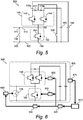
- Figure 5 shows a circuit diagram illustrating the electrical arrangement of elements of a converter module 500 based on a half-bridge cell topology.
- the converter module 500 shown in Figure 5 is equivalent to the converter module 100 described with reference to Figure 1 except that the resistor (or resistive component) connecting the first electrical current path to the second electrical current path includes two separate resistor elements 175a and 175b.
- Figure 5 shows that the two separate resistor elements (or resistive elements) 175a and 175b may be connected in series at a node 577 connected to the second node 190 through a switch 550, such as e.g. a semiconductor switch or a mechanical switch.
- a switch 550 such as e.g. a semiconductor switch or a mechanical switch.
- the present disclosure relates also to a device comprising a control circuit and at least one converter module as defined in any one of the preceding embodiments.
- Figure 6 shows an embodiment of such a device 600.
- the device 600 includes a converter module 605 which may be equivalent to any one of the converter modules described in the above embodiments.
- the converter module shown in Figure 6 corresponds to the converter module 100 described with reference to Figure 1 .
- the device includes a control circuit with a controller 610, a triggering unit 620, a delay unit 630, a by-pass trigger 660 and gate units 640 and 650.
- the control circuit via the controller 610 generates a signal instructing the switching devices and the switching modules of the converter module to turn off.
- the gates of the switching devices of the first switching module may be connected to a common control line which may receive a control signal to deactivate the switching devices (the transistors) upon detection of a failure.
- the gates of the switching devices of the switching modules may be connected to separate control lines such that the control unit is configured to send separate control signals to the switching devices via the separate control lines.
- two gate units 640 and 650 connected to the controller 610 are configured to deactivate (turn off) the first switching module and the second switching module, respectively, of the converter module 605 upon reception of a signal from the controller 610 via the triggering unit 620.
- control circuit via the controller 610 and the triggering unit 620 may be configured to synchronize activation and deactivation of the switching devices of the converter module. Further, the control circuit may be configured to instruct the by-pass switch to conduct current upon detection of a failure. In particular, the control circuit via the controller 610 may be configured to trigger the by-pass switch after a delay has elapsed since transmission of instructions to turn off the switching devices of the converter module. For this purpose, the control circuit may be equipped with a delay unit 630 to delay the triggering signal transmitted to the by-pass trigger unit 660 connected to the by-pass switch of the converter module for activation.
- control unit may be configured to force to turn off all the transistors connected in parallel such that, in case one of the transistors is in short circuit failure, the other transistors are turned off. Then, after the by-pass switch is triggered, only one of the capacitor units will be discharged through the failed IGBT and the by-pass switch. The other capacitor unit will experience a very slow discharge through its internal resistor.
- the capacitor units when the switching modules are turned on, the capacitor units will experience approximately the same voltage level during their charge/discharge process. Using capacitances of approximately the same value for the capacitor units (with a difference in the range of about 5-10%), the amount of charge/discharge will also be similar and the current though the switching modules will be balanced (with about 5-10% difference).
- the present disclosure also relates to a valve unit or, more generally, a power converter station comprising a plurality of converter modules or devices as defined in any one of the preceding embodiments.
- the plurality of converter modules may be connected in series and arranged as at least one column.
- converter modules based on either half bridge topology or full bridge topology are provided.
- the converter module may include a first switching module and a second switching module.
- the first switching module includes at least two switching devices connected in parallel and the second switching module is connected from a first node to a second node.
- the second switching module is connected in series with the first switching module via the first node.
- the converter module includes at least two capacitor units dedicated to each one of the at least two switching devices of the first switching module such that a first capacitor unit is separately connected from the first node to a first switching device of the first switching module and a second capacitor unit is separately connected from the first node to a second switching device of the first switching module.
- the first node may be connected to a first connection line and the second node may be connected to a second connection line.
- a by-pass switch is connected in parallel with the second switching module between the first connection line and the second connection line.
- the converter module comprises a first switching module and a second switching module.
- the first switching module includes at least two switching devices connected in parallel and the second switching module is connected from a first node to a second node.
- the second switching module may be connected in series with the first switching module via the first node.
- the converter module includes at least two capacitor units separately connected to the two switching devices of the first switching module such that a first capacitor unit is connected from the second node to a first switching device of the first switching module and a second capacitor unit is connected from the second node to a second switching device of the first switching module.
- the converter module further includes a third switching module including at least two switching devices connected in parallel and a fourth switching module connected between the second node and a third node.
- the fourth switching module is connected in series with the third switching module via the third node, wherein a first switching device of the third switching module is connected to the second node via the first capacitor unit and a second switching device of the third switching module is connected to the second node via the second capacitor unit.
- the first node is connected to a first connection line while the third node is connected to a second connection line.
- the converter module includes a by-pass switch connected between the first node and the third node (i.e. between the two connection lines).
- valve unit may be interchangeably replaced with the terms converter valve stack, block unit or apparatus (of a power converter).
- the embodiments of the present disclosure are advantageous in any applications wherein constraints on a by-pass switch are to be alleviated or wherein it is required to reduce the amount of energy released in case of failure of one or more transistors of a converter module.
- the embodiments of the present disclosure are therefore particularly advantageous for applications in which a more compact power equipment is desired in order to reduce the stress from energy release during converter module failure.
- An example may be electric power equipments for offshore wind farm applications.
- the present disclosure is applicable for power equipments with various voltage levels such as e.g. a high voltage power converter station but also medium voltage equipments.
- embodiments of the present disclosure may be beneficial to achieve converters such as a static synchronous compensator (STATCOM) for flexible AC transmission systems (FACTS) applications, motor drives, sub-sea power converters and DC-DC converters for DC grid.
- STATCOM static synchronous compensator
- FACTS flexible AC transmission systems
- Other applications may however be envisaged.
- valve units 4 and 6 include five valve units, it will be appreciated that any other number of valve units may be used to form a power converter station (or at least part of it). Further, reference to a first, second, third, fourth and fifth valve units may be interchanged such as for instance the third valve unit is considered to be the first valve unit and vice versa.
Claims (15)
- Module convertisseur (100, 500) comprenant :une première borne (110) pour l'entrée/la sortie d'un courant électrique dans le module convertisseur par l'intermédiaire d'une première ligne de connexion (112),une seconde borne (120) pour la sortie/l'entrée du courant du module convertisseur par l'intermédiaire d'une seconde ligne de connexion (122),un commutateur de dérivation (130) connecté entre la première borne et la seconde borne,un premier module de commutation (140) et un deuxième module de commutation (150) connectés en série par l'intermédiaire d'un premier nœud (180) connecté à l'une ou l'autre de la première borne (110) et de la seconde borne (120),dans lequel au moins le premier module de commutation (140) comporte deux dispositifs de commutation (142, 144) et dans lequel le deuxième module de commutation (150) est connecté entre le premier nœud et un deuxième nœud (190),au moins deux unités de condensateurs (160, 170), dans lequel une première unité de condensateur (160) est connectée à partir du deuxième nœud à un premier dispositif de commutation (142) du premier module de commutation et une deuxième unité de condensateur (170) est connectée à partir du deuxième nœud à un deuxième dispositif de commutation (144) du premier module de commutation pour former deux chemins de courant séparés entre le premier nœud et le deuxième nœud, etau moins un composant résistif (175), dans lequel un premier chemin de courant connectant la première unité de condensateur (160) au premier dispositif de commutation (142) du premier module de commutation (140) est connecté par l'intermédiaire dudit au moins un composant résistif (175) à un second chemin de courant connectant la deuxième unité de condensateur (170) au deuxième dispositif de commutation (144) du premier module de commutation (140),dans lequel ledit au moins un composant résistif (175) comporte au moins deux éléments de résistance séparés (175a, 175b) connectés en série au niveau d'un nœud (577) connecté au deuxième nœud (190) par le biais d'au moins un commutateur à semi-conducteur ou d'un commutateur mécanique (550) compris dans le module convertisseur (100, 500).
- Module convertisseur selon la revendication 1, le premier module de commutation comportant une pluralité de dispositifs de commutation (242, 244, 246, 248) et le module convertisseur comprenant une pluralité d'unités de condensateurs (262, 264, 266, 268), dans lequel chacune des unités de condensateurs est connectée séparément à un dispositif correspondant des dispositifs de commutation du premier module de commutation.
- Module convertisseur selon la revendication 1 ou 2, dans lequel un dispositif de commutation du premier module de commutation comporte un transistor présentant un émetteur (142c), une grille (142b) et un collecteur (142a).
- Module convertisseur selon la revendication 3, dans lequel le deuxième module de commutation est connecté au niveau du premier nœud soit aux émetteurs, soit aux collecteurs des dispositifs de commutation du premier module de commutation.
- Module convertisseur selon l'une quelconque des revendications 3 et 4, dans lequel les grilles des dispositifs de commutation du premier module de commutation sont connectées à une ligne de commande commune ou à des lignes de commande séparées.
- Module convertisseur selon l'une quelconque des revendications précédentes, dans lequel le deuxième module de commutation comporte un ou plusieurs dispositifs de commutation.
- Module convertisseur selon l'une quelconque des revendications précédentes, dans lequel un dispositif de commutation du premier module de commutation ou un dispositif de commutation du deuxième module de commutation est l'un d'un transistor bipolaire à grille isolée (IGBT), d'un transistor bi-mode à grille isolée (BIGT), d'un transistor à effet de champ à semi-conducteur métal oxyde (MOSFET), d'un thyristor commuté par la gâchette intégré (IGCT), d'un thyristor à extinction par la gâchette (GTO), d'un transistor à haute mobilité d'électrons (HEMT) et d'un transistor bipolaire à hétérojonction (HBT).
- Module convertisseur selon l'une quelconque des revendications précédentes, dans lequel le commutateur de dérivation est connecté en parallèle avec le deuxième module de commutation entre le premier nœud et le deuxième nœud.
- Module convertisseur selon l'une quelconque des revendications 1 à 7, comprenant en outre un troisième module de commutation (405) et un quatrième module de commutation (415) connectés en série par l'intermédiaire d'un troisième nœud (482), dans lequel le troisième module de commutation comporte au moins deux dispositifs de commutation (406, 407) et dans lequel le quatrième module de commutation est connecté entre le deuxième nœud et le troisième nœud, dans lequel un premier dispositif de commutation (406) du troisième module de commutation est connecté au deuxième nœud par l'intermédiaire de la première unité de condensateur et un deuxième dispositif de commutation (407) du troisième module de commutation est connecté au deuxième nœud par l'intermédiaire du deuxième condensateur pour former deux chemins de courant séparés entre le troisième nœud et le deuxième nœud.
- Module convertisseur selon la revendication 9, dans lequel le commutateur de dérivation est connecté entre le premier nœud et le troisième nœud.
- Dispositif comprenant un circuit de commande et au moins un module convertisseur tel que défini dans l'une quelconque des revendications précédentes, dans lequel le circuit de commande est configuré pour déclencher le commutateur de dérivation dudit module convertisseur et pour générer un signal donnant pour instruction aux dispositifs de commutation et aux modules de commutation dudit au moins un module convertisseur de s'arrêter.
- Dispositif selon la revendication 11, dans lequel le circuit de commande est configuré pour donner pour instruction au commutateur de dérivation de conduire le courant et aux dispositifs de communication et modules de commutation de s'arrêter à la détection d'une défaillance au niveau de l'un quelconque des dispositifs de commutation du premier module de commutation ou du troisième module de commutation dudit au moins un module convertisseur et/ou à la détection d'une défaillance au niveau de l'un quelconque du deuxième module de commutation ou du quatrième module de commutation dudit au moins un module convertisseur.
- Dispositif selon la revendication 11 ou 12, dans lequel le circuit de commande est configuré pour déclencher le commutateur de dérivation après l'écoulement d'un délai depuis la transmission d'instructions d'arrêt des dispositifs de commutation du module convertisseur.
- Dispositif selon l'une quelconque des revendications 11 à 13, dans lequel le circuit de commande est configuré pour synchroniser l'activation et la désactivation des dispositifs de commutation du module convertisseur.
- Station de conversion de puissance comprenant une pluralité de modules convertisseurs ou de dispositifs selon l'une quelconque des revendications précédentes, ladite pluralité de modules convertisseurs étant connectée en série et agencée sous forme d'au moins une colonne.
Applications Claiming Priority (1)
| Application Number | Priority Date | Filing Date | Title |
|---|---|---|---|
| PCT/EP2016/052959 WO2017137088A1 (fr) | 2016-02-12 | 2016-02-12 | Module convertisseur pour station d'énergie hvdc |
Publications (2)
| Publication Number | Publication Date |
|---|---|
| EP3414819A1 EP3414819A1 (fr) | 2018-12-19 |
| EP3414819B1 true EP3414819B1 (fr) | 2020-01-08 |
Family
ID=55349848
Family Applications (1)
| Application Number | Title | Priority Date | Filing Date |
|---|---|---|---|
| EP16703993.2A Active EP3414819B1 (fr) | 2016-02-12 | 2016-02-12 | Module de convertisseur pour une centrale de transmission à haute tension à courant continu |
Country Status (4)
| Country | Link |
|---|---|
| US (1) | US10284076B2 (fr) |
| EP (1) | EP3414819B1 (fr) |
| CN (1) | CN108702083B (fr) |
| WO (1) | WO2017137088A1 (fr) |
Families Citing this family (5)
| Publication number | Priority date | Publication date | Assignee | Title |
|---|---|---|---|---|
| WO2017203865A1 (fr) * | 2016-05-25 | 2017-11-30 | 三菱電機株式会社 | Convertisseur électrique |
| EP3485565B1 (fr) * | 2016-09-05 | 2020-05-27 | Siemens Aktiengesellschaft | Procédé de décharge d'un accumulateur d'énergie électrique |
| WO2019149367A1 (fr) * | 2018-02-02 | 2019-08-08 | Siemens Aktiengesellschaft | Convertisseur redresseur modulaire à plusieurs étages et module de commutation pour convertisseur redresseur modulaire à plusieurs étages |
| EP3621191A1 (fr) * | 2018-09-06 | 2020-03-11 | ABB Schweiz AG | Connexion parallèle à l'intérieur de cellules mmc par découplage de section cc |
| US20230144976A1 (en) * | 2021-11-08 | 2023-05-11 | Hamilton Sundstrand Corporation | High voltage dc systems |
Family Cites Families (14)
| Publication number | Priority date | Publication date | Assignee | Title |
|---|---|---|---|---|
| US8462530B2 (en) * | 2006-12-21 | 2013-06-11 | Siemens Aktiengesellschaft | Converter with short-circuit current limiting |
| CN102163907B (zh) * | 2011-01-28 | 2014-03-12 | 中国电力科学研究院 | 一种基于全控器件的电压源换流器基本功能单元 |
| CN103891124A (zh) * | 2011-07-29 | 2014-06-25 | Abb技术有限公司 | Ctl单元保护 |
| CN103947099B (zh) * | 2011-11-15 | 2017-04-05 | 阿尔斯通技术有限公司 | 功率电子模块 |
| US9425705B2 (en) * | 2012-08-13 | 2016-08-23 | Rockwell Automation Technologies, Inc. | Method and apparatus for bypassing cascaded H-bridge (CHB) power cells and power sub cell for multilevel inverter |
| JP6106072B2 (ja) * | 2013-12-09 | 2017-03-29 | 東芝三菱電機産業システム株式会社 | 電力変換装置 |
| DK2887526T3 (da) * | 2013-12-19 | 2019-06-24 | Abb Schweiz Ag | Fremgangsmåde og strømretter til at bestemme forringelse af en cellekondensator i en omformercelle |
| US10186952B2 (en) * | 2014-03-05 | 2019-01-22 | Mitsubishi Electric Corporation | Power conversion device |
| CN103915808B (zh) | 2014-03-07 | 2018-07-31 | 南方电网科学研究院有限责任公司 | 基于电压源型换流器的直流融冰装置及其控制方法 |
| KR101897725B1 (ko) * | 2014-04-08 | 2018-09-12 | 지멘스 악티엔게젤샤프트 | 과전류 손상으로부터 전기적 모듈러 유닛을 보호하기 위한 방법 |
| WO2016002319A1 (fr) * | 2014-06-30 | 2016-01-07 | 三菱電機株式会社 | Dispositif de conversion de puissance |
| EP2975723B1 (fr) * | 2014-07-16 | 2019-10-09 | General Electric Technology GmbH | Régulateur de flux de courant |
| EP2980981A1 (fr) * | 2014-07-30 | 2016-02-03 | Alstom Technology Ltd | Améliorations apportées ou relatives à des ensembles électriques pour sous-modules de source de tension |
| CN208433908U (zh) * | 2015-05-28 | 2019-01-25 | 西门子公司 | 电压源换流器模块和换流器 |
-
2016
- 2016-02-12 US US16/070,479 patent/US10284076B2/en active Active
- 2016-02-12 EP EP16703993.2A patent/EP3414819B1/fr active Active
- 2016-02-12 WO PCT/EP2016/052959 patent/WO2017137088A1/fr active Application Filing
- 2016-02-12 CN CN201680081892.XA patent/CN108702083B/zh active Active
Non-Patent Citations (1)
| Title |
|---|
| None * |
Also Published As
| Publication number | Publication date |
|---|---|
| CN108702083A (zh) | 2018-10-23 |
| EP3414819A1 (fr) | 2018-12-19 |
| CN108702083B (zh) | 2020-09-18 |
| US10284076B2 (en) | 2019-05-07 |
| WO2017137088A1 (fr) | 2017-08-17 |
| US20190028020A1 (en) | 2019-01-24 |
Similar Documents
| Publication | Publication Date | Title |
|---|---|---|
| EP3414819B1 (fr) | Module de convertisseur pour une centrale de transmission à haute tension à courant continu | |
| EP2781013B1 (fr) | Module électronique de puissance | |
| US9806599B2 (en) | Converter submodule with short-circuit device and power converter having same | |
| RU2563034C2 (ru) | Инвертор для высоких напряжений | |
| US9214877B2 (en) | Gate driving circuit having a fault detecting circuit for a semiconductor switching device | |
| US9190924B2 (en) | Indirect matrix converter | |
| US10601340B2 (en) | Submodule and electrical arrangement having submodules | |
| US20120212983A1 (en) | Method for converting power for a high-voltage direct voltage connection | |
| JP6334201B2 (ja) | 電力変換装置、及び電力変換装置の制御方法 | |
| US9525348B1 (en) | Power converter having integrated capacitor-blocked transistor cells | |
| US11632059B1 (en) | Submodule topology circuit for modular multilevel converter and method for controlling same | |
| WO2018006970A1 (fr) | Pile d'énergie à semi-conducteur d'un convertisseur modulaire multiniveaux | |
| US20210013816A1 (en) | Voltage source converter apparatus | |
| WO2018145724A1 (fr) | Système de circuit de protection | |
| EP3813239A1 (fr) | Circuit à alimentation autonome et dispositif de conversion de courant | |
| US10243482B2 (en) | Solid-state power converters | |
| US11362654B2 (en) | Auxiliary circuit | |
| Nguyen et al. | A novel submodule topology of MMC for blocking DC-fault currents in HVDC transmission systems | |
| EP3574576B1 (fr) | Agencement de protection pour un sous-module d'un mmc-hvdc | |
| US20130114314A1 (en) | Converter system and power electronic system comprising such converter systems | |
| US9564833B2 (en) | Solid-state inverters with voltage-balanced switches | |
| US20210143750A1 (en) | Modular Inverter | |
| WO2020243817A1 (fr) | Sous-module demi-pont modifié pour convertisseur multi-niveaux de source de tension avec capacité de suppression de défaut de courant continu et procédé associé | |
| WO2016058639A1 (fr) | Circuit convertisseur de puissance | |
| EP3493343A1 (fr) | Agencement de circuit |
Legal Events
| Date | Code | Title | Description |
|---|---|---|---|
| STAA | Information on the status of an ep patent application or granted ep patent |
Free format text: STATUS: THE INTERNATIONAL PUBLICATION HAS BEEN MADE |
|
| PUAI | Public reference made under article 153(3) epc to a published international application that has entered the european phase |
Free format text: ORIGINAL CODE: 0009012 |
|
| STAA | Information on the status of an ep patent application or granted ep patent |
Free format text: STATUS: REQUEST FOR EXAMINATION WAS MADE |
|
| 17P | Request for examination filed |
Effective date: 20180912 |
|
| AK | Designated contracting states |
Kind code of ref document: A1 Designated state(s): AL AT BE BG CH CY CZ DE DK EE ES FI FR GB GR HR HU IE IS IT LI LT LU LV MC MK MT NL NO PL PT RO RS SE SI SK SM TR |
|
| AX | Request for extension of the european patent |
Extension state: BA ME |
|
| DAV | Request for validation of the european patent (deleted) | ||
| DAX | Request for extension of the european patent (deleted) | ||
| GRAP | Despatch of communication of intention to grant a patent |
Free format text: ORIGINAL CODE: EPIDOSNIGR1 |
|
| STAA | Information on the status of an ep patent application or granted ep patent |
Free format text: STATUS: GRANT OF PATENT IS INTENDED |
|
| INTG | Intention to grant announced |
Effective date: 20190830 |
|
| GRAS | Grant fee paid |
Free format text: ORIGINAL CODE: EPIDOSNIGR3 |
|
| GRAA | (expected) grant |
Free format text: ORIGINAL CODE: 0009210 |
|
| STAA | Information on the status of an ep patent application or granted ep patent |
Free format text: STATUS: THE PATENT HAS BEEN GRANTED |
|
| AK | Designated contracting states |
Kind code of ref document: B1 Designated state(s): AL AT BE BG CH CY CZ DE DK EE ES FI FR GB GR HR HU IE IS IT LI LT LU LV MC MK MT NL NO PL PT RO RS SE SI SK SM TR |
|
| REG | Reference to a national code |
Ref country code: GB Ref legal event code: FG4D |
|
| REG | Reference to a national code |
Ref country code: CH Ref legal event code: EP |
|
| REG | Reference to a national code |
Ref country code: DE Ref legal event code: R096 Ref document number: 602016027754 Country of ref document: DE |
|
| REG | Reference to a national code |
Ref country code: IE Ref legal event code: FG4D |
|
| REG | Reference to a national code |
Ref country code: AT Ref legal event code: REF Ref document number: 1223905 Country of ref document: AT Kind code of ref document: T Effective date: 20200215 |
|
| REG | Reference to a national code |
Ref country code: NL Ref legal event code: MP Effective date: 20200108 |
|
| REG | Reference to a national code |
Ref country code: LT Ref legal event code: MG4D |
|
| PG25 | Lapsed in a contracting state [announced via postgrant information from national office to epo] |
Ref country code: LT Free format text: LAPSE BECAUSE OF FAILURE TO SUBMIT A TRANSLATION OF THE DESCRIPTION OR TO PAY THE FEE WITHIN THE PRESCRIBED TIME-LIMIT Effective date: 20200108 Ref country code: RS Free format text: LAPSE BECAUSE OF FAILURE TO SUBMIT A TRANSLATION OF THE DESCRIPTION OR TO PAY THE FEE WITHIN THE PRESCRIBED TIME-LIMIT Effective date: 20200108 Ref country code: NL Free format text: LAPSE BECAUSE OF FAILURE TO SUBMIT A TRANSLATION OF THE DESCRIPTION OR TO PAY THE FEE WITHIN THE PRESCRIBED TIME-LIMIT Effective date: 20200108 Ref country code: NO Free format text: LAPSE BECAUSE OF FAILURE TO SUBMIT A TRANSLATION OF THE DESCRIPTION OR TO PAY THE FEE WITHIN THE PRESCRIBED TIME-LIMIT Effective date: 20200408 Ref country code: PT Free format text: LAPSE BECAUSE OF FAILURE TO SUBMIT A TRANSLATION OF THE DESCRIPTION OR TO PAY THE FEE WITHIN THE PRESCRIBED TIME-LIMIT Effective date: 20200531 Ref country code: FI Free format text: LAPSE BECAUSE OF FAILURE TO SUBMIT A TRANSLATION OF THE DESCRIPTION OR TO PAY THE FEE WITHIN THE PRESCRIBED TIME-LIMIT Effective date: 20200108 |
|
| PG25 | Lapsed in a contracting state [announced via postgrant information from national office to epo] |
Ref country code: SE Free format text: LAPSE BECAUSE OF FAILURE TO SUBMIT A TRANSLATION OF THE DESCRIPTION OR TO PAY THE FEE WITHIN THE PRESCRIBED TIME-LIMIT Effective date: 20200108 Ref country code: LV Free format text: LAPSE BECAUSE OF FAILURE TO SUBMIT A TRANSLATION OF THE DESCRIPTION OR TO PAY THE FEE WITHIN THE PRESCRIBED TIME-LIMIT Effective date: 20200108 Ref country code: HR Free format text: LAPSE BECAUSE OF FAILURE TO SUBMIT A TRANSLATION OF THE DESCRIPTION OR TO PAY THE FEE WITHIN THE PRESCRIBED TIME-LIMIT Effective date: 20200108 Ref country code: GR Free format text: LAPSE BECAUSE OF FAILURE TO SUBMIT A TRANSLATION OF THE DESCRIPTION OR TO PAY THE FEE WITHIN THE PRESCRIBED TIME-LIMIT Effective date: 20200409 Ref country code: IS Free format text: LAPSE BECAUSE OF FAILURE TO SUBMIT A TRANSLATION OF THE DESCRIPTION OR TO PAY THE FEE WITHIN THE PRESCRIBED TIME-LIMIT Effective date: 20200508 Ref country code: BG Free format text: LAPSE BECAUSE OF FAILURE TO SUBMIT A TRANSLATION OF THE DESCRIPTION OR TO PAY THE FEE WITHIN THE PRESCRIBED TIME-LIMIT Effective date: 20200408 |
|
| REG | Reference to a national code |
Ref country code: CH Ref legal event code: PL |
|
| REG | Reference to a national code |
Ref country code: DE Ref legal event code: R097 Ref document number: 602016027754 Country of ref document: DE |
|
| REG | Reference to a national code |
Ref country code: BE Ref legal event code: MM Effective date: 20200229 |
|
| PG25 | Lapsed in a contracting state [announced via postgrant information from national office to epo] |
Ref country code: RO Free format text: LAPSE BECAUSE OF FAILURE TO SUBMIT A TRANSLATION OF THE DESCRIPTION OR TO PAY THE FEE WITHIN THE PRESCRIBED TIME-LIMIT Effective date: 20200108 Ref country code: SK Free format text: LAPSE BECAUSE OF FAILURE TO SUBMIT A TRANSLATION OF THE DESCRIPTION OR TO PAY THE FEE WITHIN THE PRESCRIBED TIME-LIMIT Effective date: 20200108 Ref country code: CZ Free format text: LAPSE BECAUSE OF FAILURE TO SUBMIT A TRANSLATION OF THE DESCRIPTION OR TO PAY THE FEE WITHIN THE PRESCRIBED TIME-LIMIT Effective date: 20200108 Ref country code: ES Free format text: LAPSE BECAUSE OF FAILURE TO SUBMIT A TRANSLATION OF THE DESCRIPTION OR TO PAY THE FEE WITHIN THE PRESCRIBED TIME-LIMIT Effective date: 20200108 Ref country code: MC Free format text: LAPSE BECAUSE OF FAILURE TO SUBMIT A TRANSLATION OF THE DESCRIPTION OR TO PAY THE FEE WITHIN THE PRESCRIBED TIME-LIMIT Effective date: 20200108 Ref country code: EE Free format text: LAPSE BECAUSE OF FAILURE TO SUBMIT A TRANSLATION OF THE DESCRIPTION OR TO PAY THE FEE WITHIN THE PRESCRIBED TIME-LIMIT Effective date: 20200108 Ref country code: SM Free format text: LAPSE BECAUSE OF FAILURE TO SUBMIT A TRANSLATION OF THE DESCRIPTION OR TO PAY THE FEE WITHIN THE PRESCRIBED TIME-LIMIT Effective date: 20200108 Ref country code: LU Free format text: LAPSE BECAUSE OF NON-PAYMENT OF DUE FEES Effective date: 20200212 Ref country code: DK Free format text: LAPSE BECAUSE OF FAILURE TO SUBMIT A TRANSLATION OF THE DESCRIPTION OR TO PAY THE FEE WITHIN THE PRESCRIBED TIME-LIMIT Effective date: 20200108 |
|
| PLBE | No opposition filed within time limit |
Free format text: ORIGINAL CODE: 0009261 |
|
| STAA | Information on the status of an ep patent application or granted ep patent |
Free format text: STATUS: NO OPPOSITION FILED WITHIN TIME LIMIT |
|
| REG | Reference to a national code |
Ref country code: AT Ref legal event code: MK05 Ref document number: 1223905 Country of ref document: AT Kind code of ref document: T Effective date: 20200108 |
|
| PG25 | Lapsed in a contracting state [announced via postgrant information from national office to epo] |
Ref country code: LI Free format text: LAPSE BECAUSE OF NON-PAYMENT OF DUE FEES Effective date: 20200229 Ref country code: CH Free format text: LAPSE BECAUSE OF NON-PAYMENT OF DUE FEES Effective date: 20200229 |
|
| 26N | No opposition filed |
Effective date: 20201009 |
|
| PG25 | Lapsed in a contracting state [announced via postgrant information from national office to epo] |
Ref country code: AT Free format text: LAPSE BECAUSE OF FAILURE TO SUBMIT A TRANSLATION OF THE DESCRIPTION OR TO PAY THE FEE WITHIN THE PRESCRIBED TIME-LIMIT Effective date: 20200108 Ref country code: IE Free format text: LAPSE BECAUSE OF NON-PAYMENT OF DUE FEES Effective date: 20200212 Ref country code: IT Free format text: LAPSE BECAUSE OF FAILURE TO SUBMIT A TRANSLATION OF THE DESCRIPTION OR TO PAY THE FEE WITHIN THE PRESCRIBED TIME-LIMIT Effective date: 20200108 |
|
| PG25 | Lapsed in a contracting state [announced via postgrant information from national office to epo] |
Ref country code: BE Free format text: LAPSE BECAUSE OF NON-PAYMENT OF DUE FEES Effective date: 20200229 Ref country code: SI Free format text: LAPSE BECAUSE OF FAILURE TO SUBMIT A TRANSLATION OF THE DESCRIPTION OR TO PAY THE FEE WITHIN THE PRESCRIBED TIME-LIMIT Effective date: 20200108 Ref country code: PL Free format text: LAPSE BECAUSE OF FAILURE TO SUBMIT A TRANSLATION OF THE DESCRIPTION OR TO PAY THE FEE WITHIN THE PRESCRIBED TIME-LIMIT Effective date: 20200108 |
|
| REG | Reference to a national code |
Ref country code: DE Ref legal event code: R081 Ref document number: 602016027754 Country of ref document: DE Owner name: HITACHI ENERGY SWITZERLAND AG, CH Free format text: FORMER OWNER: ABB SCHWEIZ AG, BADEN, CH Ref country code: DE Ref legal event code: R081 Ref document number: 602016027754 Country of ref document: DE Owner name: HITACHI ENERGY LTD, CH Free format text: FORMER OWNER: ABB SCHWEIZ AG, BADEN, CH Ref country code: DE Ref legal event code: R081 Ref document number: 602016027754 Country of ref document: DE Owner name: ABB POWER GRIDS SWITZERLAND AG, CH Free format text: FORMER OWNER: ABB SCHWEIZ AG, BADEN, CH |
|
| REG | Reference to a national code |
Ref country code: GB Ref legal event code: 732E Free format text: REGISTERED BETWEEN 20220421 AND 20220427 |
|
| PG25 | Lapsed in a contracting state [announced via postgrant information from national office to epo] |
Ref country code: TR Free format text: LAPSE BECAUSE OF FAILURE TO SUBMIT A TRANSLATION OF THE DESCRIPTION OR TO PAY THE FEE WITHIN THE PRESCRIBED TIME-LIMIT Effective date: 20200108 Ref country code: MT Free format text: LAPSE BECAUSE OF FAILURE TO SUBMIT A TRANSLATION OF THE DESCRIPTION OR TO PAY THE FEE WITHIN THE PRESCRIBED TIME-LIMIT Effective date: 20200108 Ref country code: CY Free format text: LAPSE BECAUSE OF FAILURE TO SUBMIT A TRANSLATION OF THE DESCRIPTION OR TO PAY THE FEE WITHIN THE PRESCRIBED TIME-LIMIT Effective date: 20200108 |
|
| REG | Reference to a national code |
Ref country code: DE Ref legal event code: R081 Ref document number: 602016027754 Country of ref document: DE Owner name: HITACHI ENERGY SWITZERLAND AG, CH Free format text: FORMER OWNER: ABB POWER GRIDS SWITZERLAND AG, BADEN, CH Ref country code: DE Ref legal event code: R081 Ref document number: 602016027754 Country of ref document: DE Owner name: HITACHI ENERGY LTD, CH Free format text: FORMER OWNER: ABB POWER GRIDS SWITZERLAND AG, BADEN, CH |
|
| PG25 | Lapsed in a contracting state [announced via postgrant information from national office to epo] |
Ref country code: MK Free format text: LAPSE BECAUSE OF FAILURE TO SUBMIT A TRANSLATION OF THE DESCRIPTION OR TO PAY THE FEE WITHIN THE PRESCRIBED TIME-LIMIT Effective date: 20200108 Ref country code: AL Free format text: LAPSE BECAUSE OF FAILURE TO SUBMIT A TRANSLATION OF THE DESCRIPTION OR TO PAY THE FEE WITHIN THE PRESCRIBED TIME-LIMIT Effective date: 20200108 |
|
| PGFP | Annual fee paid to national office [announced via postgrant information from national office to epo] |
Ref country code: FR Payment date: 20230221 Year of fee payment: 8 |
|
| PGFP | Annual fee paid to national office [announced via postgrant information from national office to epo] |
Ref country code: GB Payment date: 20230221 Year of fee payment: 8 Ref country code: DE Payment date: 20230216 Year of fee payment: 8 |
|
| P01 | Opt-out of the competence of the unified patent court (upc) registered |
Effective date: 20230527 |
|
| REG | Reference to a national code |
Ref country code: DE Ref legal event code: R082 Ref document number: 602016027754 Country of ref document: DE Representative=s name: DENNEMEYER & ASSOCIATES S.A., DE Ref country code: DE Ref legal event code: R081 Ref document number: 602016027754 Country of ref document: DE Owner name: HITACHI ENERGY LTD, CH Free format text: FORMER OWNER: HITACHI ENERGY SWITZERLAND AG, BADEN, CH |