EP3413348A1 - Semiconductor device and method for manufacturing semiconductor device - Google Patents
Semiconductor device and method for manufacturing semiconductor device Download PDFInfo
- Publication number
- EP3413348A1 EP3413348A1 EP16822597.7A EP16822597A EP3413348A1 EP 3413348 A1 EP3413348 A1 EP 3413348A1 EP 16822597 A EP16822597 A EP 16822597A EP 3413348 A1 EP3413348 A1 EP 3413348A1
- Authority
- EP
- European Patent Office
- Prior art keywords
- intermediate layer
- section
- connector
- board
- resin
- Prior art date
- Legal status (The legal status is an assumption and is not a legal conclusion. Google has not performed a legal analysis and makes no representation as to the accuracy of the status listed.)
- Granted
Links
Images







Classifications
-
- H—ELECTRICITY
- H10—SEMICONDUCTOR DEVICES; ELECTRIC SOLID-STATE DEVICES NOT OTHERWISE PROVIDED FOR
- H10W—GENERIC PACKAGES, INTERCONNECTIONS, CONNECTORS OR OTHER CONSTRUCTIONAL DETAILS OF DEVICES COVERED BY CLASS H10
- H10W90/00—Package configurations
-
- H—ELECTRICITY
- H10—SEMICONDUCTOR DEVICES; ELECTRIC SOLID-STATE DEVICES NOT OTHERWISE PROVIDED FOR
- H10W—GENERIC PACKAGES, INTERCONNECTIONS, CONNECTORS OR OTHER CONSTRUCTIONAL DETAILS OF DEVICES COVERED BY CLASS H10
- H10W90/00—Package configurations
- H10W90/401—Package configurations characterised by multiple insulating or insulated package substrates, interposers or RDLs
-
- H—ELECTRICITY
- H10—SEMICONDUCTOR DEVICES; ELECTRIC SOLID-STATE DEVICES NOT OTHERWISE PROVIDED FOR
- H10W—GENERIC PACKAGES, INTERCONNECTIONS, CONNECTORS OR OTHER CONSTRUCTIONAL DETAILS OF DEVICES COVERED BY CLASS H10
- H10W70/00—Package substrates; Interposers; Redistribution layers [RDL]
- H10W70/60—Insulating or insulated package substrates; Interposers; Redistribution layers
- H10W70/611—Insulating or insulated package substrates; Interposers; Redistribution layers for connecting multiple chips together
-
- H—ELECTRICITY
- H10—SEMICONDUCTOR DEVICES; ELECTRIC SOLID-STATE DEVICES NOT OTHERWISE PROVIDED FOR
- H10W—GENERIC PACKAGES, INTERCONNECTIONS, CONNECTORS OR OTHER CONSTRUCTIONAL DETAILS OF DEVICES COVERED BY CLASS H10
- H10W70/00—Package substrates; Interposers; Redistribution layers [RDL]
- H10W70/60—Insulating or insulated package substrates; Interposers; Redistribution layers
- H10W70/62—Insulating or insulated package substrates; Interposers; Redistribution layers characterised by their interconnections
- H10W70/65—Shapes or dispositions of interconnections
-
- H—ELECTRICITY
- H10—SEMICONDUCTOR DEVICES; ELECTRIC SOLID-STATE DEVICES NOT OTHERWISE PROVIDED FOR
- H10W—GENERIC PACKAGES, INTERCONNECTIONS, CONNECTORS OR OTHER CONSTRUCTIONAL DETAILS OF DEVICES COVERED BY CLASS H10
- H10W72/00—Interconnections or connectors in packages
-
- H—ELECTRICITY
- H10—SEMICONDUCTOR DEVICES; ELECTRIC SOLID-STATE DEVICES NOT OTHERWISE PROVIDED FOR
- H10W—GENERIC PACKAGES, INTERCONNECTIONS, CONNECTORS OR OTHER CONSTRUCTIONAL DETAILS OF DEVICES COVERED BY CLASS H10
- H10W72/00—Interconnections or connectors in packages
- H10W72/071—Connecting or disconnecting
- H10W72/073—Connecting or disconnecting of die-attach connectors
- H10W72/07331—Connecting techniques
- H10W72/07336—Soldering or alloying
-
- H—ELECTRICITY
- H10—SEMICONDUCTOR DEVICES; ELECTRIC SOLID-STATE DEVICES NOT OTHERWISE PROVIDED FOR
- H10W—GENERIC PACKAGES, INTERCONNECTIONS, CONNECTORS OR OTHER CONSTRUCTIONAL DETAILS OF DEVICES COVERED BY CLASS H10
- H10W90/00—Package configurations
- H10W90/701—Package configurations characterised by the relative positions of pads or connectors relative to package parts
- H10W90/731—Package configurations characterised by the relative positions of pads or connectors relative to package parts of die-attach connectors
- H10W90/734—Package configurations characterised by the relative positions of pads or connectors relative to package parts of die-attach connectors between a chip and a stacked insulating package substrate, interposer or RDL
Definitions
- the present invention relates to a semiconductor device and a method for manufacturing the semiconductor device.
- JP 2011-114176 A discloses a power semiconductor device that has a power semiconductor element, a pair of metal members arranged with the power semiconductor element interposed therebetween, a pair of insulating layers laminated on a pair of heat sinks with the pair of metal members interposed therebetween, and a mold resin section charged while covering the power semiconductor element, the pair of metal members, and the pair of insulating layers.
- This type of power semiconductor device has a lot of connectors made of metal and the like.
- some of connectors are so micro that mounting is unstable. For this reason, mounting connectors in a stable state require a use of a lot of jigs.
- automatic mounting of connectors using a mounter device may be considered, the process takes too much time in case that the number of connectors is large.
- the present invention is made in consideration of such regard, and provides a semiconductor device and a method for manufacturing the semiconductor device that enable an easy mounting of a plurality of connectors.
- a semiconductor device comprises:
- the intermediate layer may have a resin board section, in which the plurality of connectors are fixed, and the resin board section may be provided with the positioning insertion section.
- the intermediate layer may have a first intermediate layer and a second intermediate layer, which is provided on the first intermediate layer, the first intermediate layer may have a first connector and a first resin board section, in which the first connector is fixed, the second intermediate layer may have a second connector and a second resin board section, in which the second connector is fixed, and each of the first resin board section and the second resin board section may be provided with the positioning insertion section, into which the positioning section is inserted.
- the semiconductor device may further comprises:
- the intermediate layer may have a first intermediate layer and a second intermediate layer, which is provided on the first intermediate layer, the first intermediate layer may have a first connector and a first resin board section, in which the first connector is fixed, the second intermediate layer may have a second connector and a second resin board section, in which the second connector is fixed, and the first resin board section or the second resin board section may be provided with the positioning insertion section, into which the positioning section is inserted.
- the first connector may protrudee from the first resin board section to the side on which the second intermediate layer is provided, and the second resin board section may be provided with a second insertion section, into which the first connector, which protrudes from the first resin board section, is inserted.
- the second connector may protrude from the second resin board section to the side on which the first intermediate layer is provided, and the first resin board section may be provided with a first insertion section, into which the second connector, which protrudes from the second resin board section, is inserted.
- a method for manufacturing a semiconductor device comprises:
- the first board has the positioning section that positions the intermediate layer, and the intermediate layer is provided with the positioning insertion section into which the positioning section is inserted.
- the connector can be connected to the first electrically conducting layer or the first electronic element by simply inserting the positioning section into the positioning insertion section, thereby allowing the semiconductor device to be easily produced.
- a semiconductor device of the present embodiment has, as illustrated in Fig. 1 , a first board 10 and an intermediate layer 20 that is provided on the first board 10.
- the first board 10 has a first board main body 10a, a first electrically conducting layer 11 that is provided on the first board main body 10a, a first electronic element 12 that is provided on the first electrically conducting layer 11, and a connecting terminal 13 that is provided on the first electrically conducting layer 11 and extends along a short direction (a vertical direction of Fig. 2(a) ).
- the two first electronic elements 12 are arranged in a line-symmetric manner with respect to a straight line that passes through the center of the semiconductor device along a short direction.
- the first electronic element 12 is provided with a terminal 12a on its top and bottom surfaces, and a solder 12b is placed on the terminal 12a. As illustrated in Fig. 1 , the bottom surface of the first board main body 10a may be provided with a heat dissipation plate 19.
- the first board 10 has a positioning section 5 that positions the intermediate layer 20.
- the intermediate layer 20 is provided with positioning insertion sections 37 and 47, into which the positioning section 5 is inserted. While in the present embodiment, a description is made using an aspect in which the intermediate layer 20 has the resin board sections 39 and 49, the present invention is not limited to the above described embodiment, and, for instance, the intermediate layer 20 may have a frame body that has been positioned so that positions of the plurality of connectors 31 and 41 are not misaligned with respect to each other and the frame body may be provided with the positioning insertion sections.
- a semiconductor device of the present embodiment may be provided with a second board 60 on an opposite side (upper side of Fig. 1 ) to the first board 10 side with respect to the intermediate layer 20.
- the top surface of a second board main body 60a may be provided with a heat dissipation plate 69.
- the intermediate layer 20 has a plurality of connectors 31 and 41 (refer to Fig. 8 and Fig. 9 ) and resin board sections 39 and 49, in which the plurality of connectors 31 and 41 are fixed.
- the first connector 31, which is to be described later, is exposed on the first board 10 side from the first resin board section 39, which is to be described later, and is connected with the first electrically conducting layer 11 or the first electronic element 12.
- the first connector 31 is exposed also on the second board 60 side from the first resin board section 39, and connected with a second electronic element 62 via a second electrically conducting layer 61.
- each of the first resin board section 39 and the second resin board section 49 may be provided with the positioning insertion section (the first positioning insertion section) 37 and the positioning insertion section (the second positioning insertion section) 47 into which the positioning section 5 is inserted.
- the first resin board section 39 is provided with the positioning insertion section 37 and the second resin board section 49 is not provided with the positioning insertion section 47.
- the second board may be provided with a positioning insertion section 67 into which the positioning section 5 is inserted.
- each of the first resin board section 39 and the second resin board section 49 may be provided with the positioning insertion sections 37 and 47 into which the positioning section 5 is inserted, only one of the first resin board section 39 and the second resin board section 49 may be provided with the positioning insertion sections 37 and 47 into which the positioning section 5 is inserted (in an aspect illustrated in Fig. 14 , the first resin board section 39 is provided with the positioning insertion sections 37), or the intermediate layer 20 may not be provided with the positioning insertion sections 37 and 47.
- the first board 10 has a plurality (three) of the positioning sections 5. While in the plan view the first board main body 10a is in a substantially rectangular shape and the connecting terminal 13 is provided on one side (lower side of Fig. 2(a) ) of long sides, each of opposite short sides is provided with the positioning section 5 and another long side on which the connecting terminal 13 is not provided of the long sides is provided with the positioning section 5.
- the intermediate layer 20 may have a first intermediate layer 30 and a second intermediate layer 40, which is provided on the first intermediate layer 30.
- the first intermediate layer 30 may have the first connector 31 and the first resin board section 39, in which the first connector 31 is fixed.
- the second intermediate layer 40 may have the second connector 41 and the second resin board section 49, in which the second connector 41 is fixed.
- the present invention is not limited to the above described embodiment, and the intermediate layer 20 may have a single layer (may have a single resin board section) or may have three or more layers (may have three or more resin board sections).
- the connectors 31 and 41 have the first connector 31 and the second connector 41.
- the first resin board section 39 has a plurality (three) of the positioning insertion sections 37.
- a position of the positioning insertion sections 37 is determined in accordance with a position of the positioning sections 5.
- the second connector 41 may protrude from the second resin board section 49 to the side on which the first intermediate layer 30 is provided, and, as illustrated in Fig. 8 , the first resin board section 39 may be provided with a first insertion section 39a, into which the second connector 41, which protrudes from the second resin board section 49, is inserted.
- the first connector 31 may protrude from the first resin board section 39 to the side on which the second intermediate layer 40 is provided, and the second resin board section 49 may be provided with a second insertion section, into which the first connector 31, which protrudes from the first resin board section 39, is inserted.
- the plurality of second connectors 41 protrude from the second resin board section 49 to the side on which the first intermediate layer 30 is provided, and are inserted into the first insertion section 39a.
- the first connector 31 may protrude from the first resin board section 39 to the first board 10 side or the second intermediate layer 40 side, may penetrate the first resin board section 39, or may be flush with the second resin board section 49 without protruding from the first resin board section 39. That is to say, the plurality of first connectors 31 may have any one or more of a protrusion type first connector 33, a penetration type first connector, and a flush type first connector.
- the plurality of first connectors 31 have the protrusion type first connector 33 that protrudes via the first resin board section 39 to the first board 10 side.
- four protrusion type first connectors 33 are provided.
- the protrusion type first connector 33 has a protrusion type first connector 33a for installation. Then, as illustrated in Fig. 4 , a top surface of the protrusion type first connector 33a for installation is made so that the second electronic element 62 is provided thereon. More specifically, the protrusion type first connector 33 has two of the protrusion type first connectors 33a for installation. Then, a top surface of each of the protrusion type first connectors 33a for installation is made so that the second electronic element 62 is provided thereon via the second electrically conducting layer 61.
- the second connector 41 which is illustrated in Fig. 9 , may protrude from the second resin board section 49 to the first intermediate layer 30 side or the other side of the first intermediate layer 30 side, may penetrate the second resin board section 49, or may be flush with the second resin board section 49 without protruding from the second resin board section 49. That is to say, the plurality of second connectors 41 may have any one or more of the protrusion type second connector 43, a penetration type second connector, and a flush type second connector.
- the second connector 41 has the protrusion type second connectors 43 and 45, which protrude from the second resin board section 49 to the first intermediate layer 30 side (back side of the paper surface of Fig. 9(a) ).
- the protrusion type second connectors 43 and 45 have the protrusion type second connector 43, which is inserted into the first insertion section 39a, and the protrusion type second connector 45, which is shorter in length than the protrusion type second connector 43.
- the protrusion type second connector 43 is made so that it is inserted into the first insertion section 39a of the first resin board section 39 illustrated in Fig. 8 . That is to say, each of the six long protrusion type second connectors 43 is made so that it is inserted into the first insertion section 39a.
- first resin board section 39 and the second resin board section 49 may be made of the same resin material, the present invention is not limited to the above described embodiment.
- the first resin board section 39 and the second resin board section 49 may be made of different resin materials.
- the first electronic element 12 and the second electronic element 62 of the present embodiment may be power devices.
- An example of power devices is a switching device. More specifically, examples of power devices have an FET such as a MOSFET, a bipolar transistor, and an IGBT, and typical examples have a MOSFET.
- the resin board sections 39 and 49 of the intermediate layer 20 may be provided with a control unit 80 that has an IC chip 81, a resistance 82, and a capacitor 83.
- the control unit 80 may be provided at the first intermediate layer 30, may be provided at the second intermediate layer 40, or may be provided at both the first intermediate layer 30 and the second intermediate layer 40.
- the control unit 80 is provided at the first intermediate layer 30.
- the control unit 80 may have a function to control the first electronic element 12 and the second electronic element 62 being power devices.
- a semiconductor device of the present embodiment may further have a mold resin section 90 (also refer to Fig. 7 ) that covers the first board 10, the first intermediate layer 30, the second intermediate layer 40, and the second board 60.
- the mold resin section 90 and the resin board sections 39 and 49 may be made of different resin materials. If the first resin board section 39 and the second resin board section 49 are made of different resin materials, a resin material of the mold resin section 90 may be different from a resin material of the first resin board section 39 and may be the same as a resin material of the second resin board section 49, or may be different from a resin material of the second resin board section 49 and may be the same as a resin material of the first resin board section 39.
- the mold resin section 90 may be made of a thermosetting resin and the resin board sections 39 and 49 may be made of a thermoplastic resin.
- thermoplastic resin is not limited in particular, a plastic or the like may be used.
- Thermoplastic resins have polyethylene, polypropylene, poly-4-methylpentene-1, ionomer, polystyrene, AS resin, ABS resin, polyvinyl chloride, polyvinylidene chloride, methacrylate resin, polyvinyl alcohol, EVA, polycarbonate, various nylon, various aromatic series or aliphatic polyester, thermoplastic polyurethane, cellulosic plastic, thermoplastic elastomer, polyarylate resin, polyethylene terephthalate, polybutylene terephthalate, polyimide, polyamide imide, polyetherimide, polysulfone, polyether sulfone, polyphenylene sulfide, polyphenyl ether, polybenzimidazole, aramid, and poly(p-phenylene benzobisoxazole) .
- Thermosetting resins are not limited, and have epoxy resin, phenolic resin, and unsaturated polyester resin, for example.
- the connectors 31 and 41 may be different in a surface area of a front surface (surface on the second board 60 side) and a rear surface (surface on the first board 10 side). More specifically, the area of the front surface of the connectors 31 and 41 may be larger than the area of the rear surface thereof.
- a front surface of the protrusion type first connectors 33a for installation (a surface on an opposite side to the first electronic element 12, that is, a top surface) is made larger than a rear surface thereof (a surface on a side of the first electronic element 12, that is, a bottom surface). Due to this, heat generated from the first electronic element 12 can be dissipated using the large front surface of the protrusion type first connectors 33a for installation while an area near the first electronic element 12 is reduced as much as possible.
- the second electronic element 62 is disposed on the protrusion type first connectors 33a for installation via the second electrically conducting layer 61, the second electronic element 62 and the front surface of the protrusion type first connectors 33a for installation can be separated from each other at a certain amount of distance.
- heat generated from the second electronic element 62 can also be dissipated using the large front surface of the protrusion type first connectors 33a for installation.
- a front surface of the protrusion type second connector 45 that is short in length (a surface on an opposite side to the second electronic element 62, that is, a top surface) is made larger than a rear surface thereof (a surface on a side of the second electronic element 62, that is, a bottom surface). Due to this, heat generated from the first electronic element 62 can be dissipated using the large front surface of the protrusion type second connector 45 while an area near the second electronic element 62 is reduced as much as possible.
- a rear surface of the first resin board section 39 (a surface on the first board 10 side) is provided with an integrally molded first protrusion section 38 that protrudes to the first board 10 side on a periphery of the first electronic element 12, and the first protrusion section 38 can prevent an unintended movement of the first electronic element 12. More specifically, the rear surface of the first resin board section 39 is provided with the first protrusion section 38 along a short direction. Although there is a possibility of an unintended movement of the first electronic element 12 before a solder (not illustrated in the drawings) placed between the first electrically conducting layer 11 and the first electronic element 12 is reflowed, such an unintended movement can be prevented in advance by providing the first protrusion section 38.
- a rear surface of the second resin board section 49 (a surface on the first board 10 side) is provided with an integrally molded second protrusion section 48 that protrudes to the first intermediate layer 30 side on a periphery of the second electronic element 62, and the second protrusion section 48 can prevent an unintended movement of the second electronic element 62. More specifically, the rear surface of the second resin board section 49 is provided with eight L-shaped second protrusion sections 48.
- provision of the second protrusion section 48 can prevent such an unintended movement in advance.
- the first board 10 that has the first electrically conducting layer 11 and the first electronic element 12 that is provided on the first electrically conducting layer 11 as illustrated in Fig. 2 is prepared.
- the solder 12b is placed on the terminal 12a of the first electronic element 12.
- the intermediate layer 20 is placed on the first board 10. In case that the intermediate layer 20 has the first intermediate layer 30 and the second intermediate layer 40, the following steps are carried out.
- the first intermediate layer 30 is placed on the first board 10 (refer to Fig. 3 ).
- the first intermediate layer 30 has, as illustrated in Fig. 8 , the protrusion type first connector 33 that protrudes from the first resin board section 39 to the first board 10 side.
- a lower end section of the protrusion type first connector 33 is placed on the solder 12b provided on the terminal 12a of the first electronic element 12 or on a solder 11b (refer to Fig. 2 ) provided on the first electrically conducting layer 11.
- an inner lower end of the pair of protrusion type first connectors 33a for installation (a lower end that is lowly positioned in the second electronic element 62) is placed on the solder 12b provided on the terminal 12a of the first electronic element 12 and an outer lower end of the two of protrusion type first connectors 33a for installation is placed on the solder 11b provided on the first electrically conducting layer 11 (also refer to Fig. 10(a) ).
- both lower ends of the protrusion type first connectors 33 that is not the protrusion type first connector 33a for installation are placed on the solder 11b provided on the first electrically conducting layer 11 (also refer to Fig. 10(a) ).
- the second electronic element 62 is provided on the top surface of the protrusion type first connector 33a for installation via the second electrically conducting layer 61.
- a solder 62b is provided on a top surface of the second electronic element 62 and a solder 61b is provided on a top surface of the second electrically conducting layer 61.
- the first intermediate layer 30 may be placed on the first board 10 after the second electronic element 62 is provided on the first intermediate layer 30 in place of adopting an aspect in which the second electronic element 62 is provided on the first intermediate layer 30 after the first intermediate layer 30 is placed on the first board 10. According to such an aspect, it is advantageous in that the second electronic element 62 can be provided on the first intermediate layer 30 in a more stable state.
- the second intermediate layer 40 is placed on the first intermediate layer 30 as illustrated in Fig. 5 .
- the first resin board section 39 of the first intermediate layer 30 is provided with a first insertion section 39a into which the protrusion type second connector 43 is inserted.
- each of the six protrusion type second connectors 43 is inserted into the first insertion section 39a.
- a part of a lower end of the protrusion type second connector 45 of the second intermediate layer 40 is placed on the solder 62b of the top surface of the second electronic element 62 and the remaining part is placed on the solder 61b of the top surface of the second electrically conducting layer 61.
- the lower end of a protrusion type second connector 45a with a large cross-sectional area is placed on the solder 62b of the top surface of the second electronic element 62 and the lower end of a protrusion type second connector 45b with a small cross-sectional area is placed on the solder 61b of the top surface of the second electrically conducting layer 61 (also refer to Fig. 10(b) ).
- the second board 60 is placed on the top surface of the second intermediate layer 40.
- an integral matter of the first board 10, the first intermediate layer 30, the second intermediate layer 40, and the second board 60 is heated at a temperature of 240°C to 260°C so that the solder is reflowed.
- the integral matter is put into a mold and a sealing material that is a material of a mold resin section 90 is poured into the mold. As a result, a semiconductor device is manufactured.
- the first board 10 has the positioning section 5 that positions the intermediate layer 20, and the intermediate layer 20 is provided with the positioning insertion sections 37 and 47 into which the positioning section 5 is inserted.
- the connectors 31 and 41 can be connected to the first electrically conducting layer 11 or the first electronic element 12 by simply inserting the positioning section 5 into the positioning insertion sections 37 and 47, thereby allowing the semiconductor device to be easily produced.
- the plurality of connectors 31 and 41 are positioned in advance and the positioning insertion sections 37 and 47 can be formed in advance. Due to this, the connectors 31 and 41 and the first electrically conducting layer 11 can be connected by simply placing on the first board 10 the connectors 31 and 41 that have already been positioned by the resin board sections 39 and 49, thereby allowing the semiconductor device to be easily produced.
- the second electronic element 62 can be laminated on the first electronic element 12 in case that an aspect is adopted in which the connector (the first connector 31) is exposed from the resin board section (the first resin board section 39) on the second board 60 side and is connected with the second electronic element 62 (refer to Fig. 9 ) .
- a position of each of the first intermediate layer 30 and the second intermediate layer 40 with respect to the first board 10 can be easily determined by the positioning section 5 in case that an aspect is adopted in which each of the first resin board section 39 of the first intermediate layer 30 and the second resin board section 49 of the second intermediate layer 40 is provided with the positioning insertion sections 37 and 47 into which the positioning section 5 is inserted.
- a position of the second board 60 with respect to the first board 10 can be easily determined by the positioning section 5 in case that an aspect in which the second board 60 is provided with the positioning insertion section 67 is adopted.
- a position of the first intermediate layer 30 or the second intermediate layer 40 that is provided with the positioning insertion sections 37 and 47 with respect to the first board 10 can be easily determined by the positioning section 5 in case that an aspect is adopted in which one of the first resin board section 39 of the first intermediate layer 30 and the second resin board section 49 of the second intermediate layer 40 is provided with the positioning insertion sections 37 and 47 into which the positioning section 5 is inserted.
- the connectors 31 and 41 can be positioned in advance with respect to the resin board sections 39 and 49 on each of the first intermediate layer 30 and the second intermediate layer 40 in case that an aspect is adopted in which the intermediate layer 20 has the first intermediate layer 30 and the second intermediate layer 40, the first intermediate layer 30 has the first resin board section 39 in which the first connector 31 is fixed, and the second intermediate layer 40 has the second resin board section 49 in which the second connector 41 is fixed (refer to Fig. 8 and Fig. 9 ).
- a relative positioning between the first intermediate layer 30 and the second intermediate layer 40 can be carried out by simply inserting into a second insertion section the first connector 31 that protrudes from the first resin board section 39 in case that an aspect is adopted in which the first connector 31 protrudes from the first resin board section 39 to a side on which the second intermediate layer 40 is provided and the second resin board section 49 is provided with the second insertion section into which the first connector 31 that protrudes from the first resin board section 39 is inserted.
- a relative positioning between the first intermediate layer 30 and the second intermediate layer 40 can be carried out by simply inserting into the first insertion section 39a the second connector 41 (the protrusion type second connector 43) that protrudes from the second resin board section 49 also in case that an aspect is adopted in which the second connector 41 protrudes from the second resin board section 49 to a side on which the first intermediate layer 30 is provided and the first resin board section 39 is provided with the first insertion section 39a into which the second connector 41 (the protrusion type second connector 43) that protrudes from the second resin board section 49 is inserted (refer to Fig. 8 and Fig. 9 ).
- a space between the first board 10 and the first intermediate layer 30 can become thicker, which is advantageous in case that there is a need for making the space thicker in terms of an arrangement of the first electronic element 12 and the like.
- the protrusion type first connector 33 that protrudes to the first board 10 side it is advantageous also in that a good solder fillet can be formed in a periphery of the protrusion type first connector 33.
- a positioning function is provided in case that an aspect is adopted in which the protrusion type first connector that protrudes to the second intermediate layer 40 side is adopted and is inserted into the second insertion section of the second intermediate layer 40. It is advantageous in that functions of both the protrusion type first connector 33 that protrudes to the first board 10 side and the protrusion type first connector that protrudes to the second intermediate layer 40 side can be provided in case that a penetration type first connector is adopted. It is advantageous in that a thickness in a thickness direction can be reduced in case that a flush type first connector is adopted.
- the first intermediate layer 30 can be placed on the first board 10 in a stable aspect in case that an aspect is adopted in which a plurality of lower ends of the protrusion type first connector (the protrusion type first connector 33 in Fig. 8 ) that protrudes to the first board 10 side are provided.
- a space between the second board 60 and the second intermediate layer 40 can become thicker, which is advantageous in case that there is a need for making the space thicker in terms of an arrangement of the second electronic element 62 and the like. It is advantageous in that the (long) protrusion type second connector 43 can be inserted into the first insertion section 39a of the first intermediate layer 30 and a positioning function can be provided, in case that an aspect is adopted in which the protrusion type second connector 43 that protrudes to the first intermediate layer 30 side is adopted and the first insertion section 39a is provided on the first intermediate layer 30.
- the (short) protrusion type second connector 45 can be easily connected to the second electrically conducting layer 61 and the second electronic element 62 in case that the protrusion type second connector 45 that protrudes to the first intermediate layer 30 side is adopted. It is advantageous in that functions of both the protrusion type second connector that protrudes to the second board 60 side and the protrusion type second connector 43 that protrudes to the first intermediate layer 30 side can be provided in case that a penetration type second connector is adopted. It is advantageous in that a thickness in a thickness direction can be reduced in case that a flush type second connector is adopted.
- first resin board section 39 and the second resin board section 49 can be provided with different functions in case that an aspect in which the first resin board section 39 and the second resin board section 49 are formed of different resin materials is adopted.
- a thickness of the second resin board section 49 is thinner than a thickness of the first resin board section 39
- a resin whose strength is higher than that of a material of the first resin board section 39 may be used as a material of the second resin board section 49.
- PEEK polyether ether ketone
- PPS polyphenylene sulfide
- PBT polybutylene terephthalate
- a possibility of malfunction can be reduced in advance because a power section and the control unit 80 can be positioned very close to each other.
- providing the control unit 80 in a semiconductor device realizes an IPM (Intelligent Power Module) .
- the resin board sections 39 and 49 that are positioned in an inner side and the mold resin section 90 that is positioned in an outer side can carry out different functions in case that an aspect in which the mold resin section 90 and the resin board sections 39 and 49 are formed of different resin materials is adopted.
- the mold resin section 90 is a thermosetting resin
- a high positioning accuracy is expected in case that a thermoplastic resin is adopted as a material of the resin board sections 39 and 49. That is to say, there is a possibility that a position of the connectors 31 and 41 is misaligned from a planned position because a hardness is not sufficient before heat is applied, in case that a thermosetting resin is used as a material of the resin board sections 39 and 49.
- thermoplastic resin as the first resin board section 39 can more securely prevent the first insertion section 39a from changing in shape or misaligning and adopting a thermoplastic resin as the second resin board section 49 can more securely prevent a position of the protrusion type second connector 43 from misaligning.
Landscapes
- Coupling Device And Connection With Printed Circuit (AREA)
- Structure Of Printed Boards (AREA)
- Combinations Of Printed Boards (AREA)
Abstract
Description
- The present invention relates to a semiconductor device and a method for manufacturing the semiconductor device.
- In the prior art, there is known an electronic element having a chip and the like and a semiconductor module that has a sealing resin that seals this electronic element. An example of the conventional semiconductor module is
JP 2011-114176 A JP 2011-114176 A - This type of power semiconductor device has a lot of connectors made of metal and the like. In addition, some of connectors are so micro that mounting is unstable. For this reason, mounting connectors in a stable state require a use of a lot of jigs. In addition, although automatic mounting of connectors using a mounter device may be considered, the process takes too much time in case that the number of connectors is large.
- The present invention is made in consideration of such regard, and provides a semiconductor device and a method for manufacturing the semiconductor device that enable an easy mounting of a plurality of connectors.
- A semiconductor device, according to the present invention, comprises:
- a first board; and
- an intermediate layer being provided on the first board and having a plurality of connectors;
- wherein the first board has a positioning section that positions the intermediate layer, and
- wherein the intermediate layer is provided with a positioning insertion section, into which the positioning section is inserted.
- In the semiconductor device according to the present invention,
the intermediate layer may have a resin board section, in which the plurality of connectors are fixed, and
the resin board section may be provided with the positioning insertion section. - In the semiconductor device according to the present invention,
the intermediate layer may have a first intermediate layer and a second intermediate layer, which is provided on the first intermediate layer,
the first intermediate layer may have a first connector and a first resin board section, in which the first connector is fixed,
the second intermediate layer may have a second connector and a second resin board section, in which the second connector is fixed, and
each of the first resin board section and the second resin board section may be provided with the positioning insertion section, into which the positioning section is inserted. - The semiconductor device, according to the present invention, may further comprises:
- a second board being provided on the intermediate layer, and
- wherein the second board may be provided with a positioning insertion section, into which the positioning section is inserted.
- In the semiconductor device according to the present invention,
the intermediate layer may have a first intermediate layer and a second intermediate layer, which is provided on the first intermediate layer,
the first intermediate layer may have a first connector and a first resin board section, in which the first connector is fixed,
the second intermediate layer may have a second connector and a second resin board section, in which the second connector is fixed, and
the first resin board section or the second resin board section may be provided with the positioning insertion section, into which the positioning section is inserted. - In the semiconductor device according to the present invention,
the first connector may protrudee from the first resin board section to the side on which the second intermediate layer is provided, and
the second resin board section may be provided with a second insertion section, into which the first connector, which protrudes from the first resin board section, is inserted. - In the semiconductor device according to the present invention,
the second connector may protrude from the second resin board section to the side on which the first intermediate layer is provided, and
the first resin board section may be provided with a first insertion section, into which the second connector, which protrudes from the second resin board section, is inserted. - A method for manufacturing a semiconductor device, according to the present invention, comprises:
- a step of preparing a first board; and
- a step of placing on the first board an intermediate layer having a plurality of connectors;
- wherein the first board has a positioning section that positions the intermediate layer, and the intermediate layer is positioned relative to the first board by inserting the positioning section into a positioning insertion section being provided in the intermediate layer.
- According to the present invention, the first board has the positioning section that positions the intermediate layer, and the intermediate layer is provided with the positioning insertion section into which the positioning section is inserted. Thus, the connector can be connected to the first electrically conducting layer or the first electronic element by simply inserting the positioning section into the positioning insertion section, thereby allowing the semiconductor device to be easily produced.
-
-
Fig. 1 is a sectional view that illustrates an outline of the structure of a semiconductor device according to an embodiment of the present invention. -
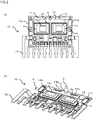
Fig. 2 (a) is a top plan view that illustrates a first board of a semiconductor device according to an embodiment of the present invention, andFig. 2(b) is a perspective view of the aspect illustrated inFig. 2(a) . -
Fig. 3(a) is a top plan view that illustrates a state in which a first intermediate layer is placed on the first board that is illustrated inFig. 2 , andFig. 3(b) is a perspective view of the aspect illustrated inFig. 3(a) . -
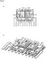
Fig. 4(a) is a top plan view that illustrates a state in which a second electrically conducting layer and a second electronic element are placed on the first intermediate layer that is illustrated inFig. 3 , andFig. 4(b) is a perspective view of the aspect illustrated inFig. 4(a) . -
Fig. 5(a) is a top plan view that illustrates a state in which a second intermediate layer is placed on the first intermediate layer, the second electrically conducting layer, and the second electronic element that are illustrated inFig. 4 , andFig. 5(b) is a perspective view of the aspect illustrated inFig. 5(a) . -
Fig. 6(a) is a top plan view that illustrates a state in which the second board is placed on the second intermediate layer that is illustrated inFig. 5 , andFig. 6(b) is a perspective view of the aspect illustrated inFig. 6(a) . -
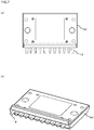
Fig. 7(a) is a top plan view that illustrates a state in which the first board, the first intermediate layer, the second intermediate layer, and the second board that are illustrated inFig. 6 are sealed with resin, andFig. 7(b) is a perspective view of the aspect illustrated inFig. 7(a) . -
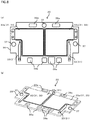
Fig. 8 (a) is a top plan view that illustrates a front surface side of a first intermediate layer according to an embodiment of the present invention, andFig. 8(b) is a perspective view of the first intermediate layer illustrated inFig. 8(a) . -
Fig. 9 (a) is a top plan view that illustrates a front surface side of a second intermediate layer according to an embodiment of the present invention, andFig. 9(b) is a perspective view of the second intermediate layer illustrated inFig. 9(a) . -
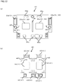
Fig. 10(a) is a bottom plan view that illustrates a rear surface side of a first intermediate layer according to an embodiment of the present invention, andFig. 10(b) is a bottom plan view that illustrates a rear surface side of a second intermediate layer according to an embodiment of the present invention. -
Fig. 11 is a top plan view of a first intermediate layer according to a variation 1 of an embodiment of the present invention. -
Fig. 12 is a sectional view that illustrates an outline of a structure of a semiconductor device according to avariation 2 of an embodiment of the present invention. -
Fig. 13 is a sectional view that illustrates an outline of a structure of a semiconductor device according to a variation 3 of an embodiment of the present invention. -
Fig. 14 is a sectional view that illustrates an outline of a structure of a semiconductor device according to a variation 4 of an embodiment of the present invention. - A semiconductor device of the present embodiment has, as illustrated in
Fig. 1 , afirst board 10 and anintermediate layer 20 that is provided on thefirst board 10. As illustrated inFig. 2 , thefirst board 10 has a first boardmain body 10a, a first electrically conductinglayer 11 that is provided on the first boardmain body 10a, a firstelectronic element 12 that is provided on the first electrically conductinglayer 11, and a connectingterminal 13 that is provided on the first electrically conductinglayer 11 and extends along a short direction (a vertical direction ofFig. 2(a) ). In the aspect illustrated inFig. 2 , the two firstelectronic elements 12 are arranged in a line-symmetric manner with respect to a straight line that passes through the center of the semiconductor device along a short direction. The firstelectronic element 12 is provided with a terminal 12a on its top and bottom surfaces, and asolder 12b is placed on the terminal 12a. As illustrated inFig. 1 , the bottom surface of the first boardmain body 10a may be provided with aheat dissipation plate 19. - The
first board 10 has apositioning section 5 that positions theintermediate layer 20. As illustrated inFig. 1 andFigs. 12 to 14 , theintermediate layer 20 is provided withpositioning insertion sections positioning section 5 is inserted. While in the present embodiment, a description is made using an aspect in which theintermediate layer 20 has theresin board sections intermediate layer 20 may have a frame body that has been positioned so that positions of the plurality ofconnectors - As illustrated in
Fig. 1 , a semiconductor device of the present embodiment may be provided with asecond board 60 on an opposite side (upper side ofFig. 1 ) to thefirst board 10 side with respect to theintermediate layer 20. The top surface of a second boardmain body 60a may be provided with aheat dissipation plate 69. - The
intermediate layer 20 has a plurality ofconnectors 31 and 41 (refer toFig. 8 andFig. 9 ) andresin board sections connectors first connector 31, which is to be described later, is exposed on thefirst board 10 side from the firstresin board section 39, which is to be described later, and is connected with the first electrically conductinglayer 11 or the firstelectronic element 12. In addition, thefirst connector 31 is exposed also on thesecond board 60 side from the firstresin board section 39, and connected with a secondelectronic element 62 via a second electrically conductinglayer 61. - As described later, in case that the
intermediate layer 20 has the firstintermediate layer 20 and the secondintermediate layer 20, as illustrated inFig. 12 , each of the firstresin board section 39 and the secondresin board section 49 may be provided with the positioning insertion section (the first positioning insertion section) 37 and the positioning insertion section (the second positioning insertion section) 47 into which thepositioning section 5 is inserted. In addition, in place of such an aspect, another aspect is acceptable in which, as illustrated inFig. 1 , the firstresin board section 39 is provided with thepositioning insertion section 37 and the secondresin board section 49 is not provided with thepositioning insertion section 47. - As illustrated in
Fig. 13 andFig. 14 , the second board may be provided with apositioning insertion section 67 into which thepositioning section 5 is inserted. In case that theintermediate layer 20 has the firstintermediate layer 20 and the secondintermediate layer 20, as illustrated inFig. 13 , each of the firstresin board section 39 and the secondresin board section 49 may be provided with thepositioning insertion sections positioning section 5 is inserted, only one of the firstresin board section 39 and the secondresin board section 49 may be provided with thepositioning insertion sections positioning section 5 is inserted (in an aspect illustrated inFig. 14 , the firstresin board section 39 is provided with the positioning insertion sections 37), or theintermediate layer 20 may not be provided with thepositioning insertion sections - In the present embodiment, a description is made below mainly using an aspect, as illustrated in
Fig. 1 , in which the firstresin board section 39 is provided with thepositioning insertion section 37 and the secondresin board section 49 is not provided with thepositioning insertion section 47. More specifically, as illustrated inFig. 2 , thefirst board 10 has a plurality (three) of thepositioning sections 5. While in the plan view the first boardmain body 10a is in a substantially rectangular shape and the connectingterminal 13 is provided on one side (lower side ofFig. 2(a) ) of long sides, each of opposite short sides is provided with thepositioning section 5 and another long side on which the connectingterminal 13 is not provided of the long sides is provided with thepositioning section 5. - As illustrated in
Fig. 1 , theintermediate layer 20 may have a firstintermediate layer 30 and a secondintermediate layer 40, which is provided on the firstintermediate layer 30. As illustrated inFig. 8 , the firstintermediate layer 30 may have thefirst connector 31 and the firstresin board section 39, in which thefirst connector 31 is fixed. As illustrated inFig. 9 , the secondintermediate layer 40 may have thesecond connector 41 and the secondresin board section 49, in which thesecond connector 41 is fixed. While in the present embodiment, a description is made using an aspect in which theintermediate layer 20 has the firstintermediate layer 30 and the secondintermediate layer 40, the present invention is not limited to the above described embodiment, and theintermediate layer 20 may have a single layer (may have a single resin board section) or may have three or more layers (may have three or more resin board sections). In the aspect in which theintermediate layer 20 has the firstintermediate layer 30 and the secondintermediate layer 40, theconnectors first connector 31 and thesecond connector 41. - As illustrated in
Fig. 8 , the firstresin board section 39 has a plurality (three) of thepositioning insertion sections 37. A position of thepositioning insertion sections 37 is determined in accordance with a position of thepositioning sections 5. - As illustrated in
Fig. 9(b) , thesecond connector 41 may protrude from the secondresin board section 49 to the side on which the firstintermediate layer 30 is provided, and, as illustrated inFig. 8 , the firstresin board section 39 may be provided with afirst insertion section 39a, into which thesecond connector 41, which protrudes from the secondresin board section 49, is inserted. In place of such an aspect or in combination with such an aspect, thefirst connector 31 may protrude from the firstresin board section 39 to the side on which the secondintermediate layer 40 is provided, and the secondresin board section 49 may be provided with a second insertion section, into which thefirst connector 31, which protrudes from the firstresin board section 39, is inserted. In the present embodiment, a description is made using an aspect in which the plurality of second connectors 41 (a long, protrusion typesecond connector 43, to be described later) protrude from the secondresin board section 49 to the side on which the firstintermediate layer 30 is provided, and are inserted into thefirst insertion section 39a. - The
first connector 31 may protrude from the firstresin board section 39 to thefirst board 10 side or the secondintermediate layer 40 side, may penetrate the firstresin board section 39, or may be flush with the secondresin board section 49 without protruding from the firstresin board section 39. That is to say, the plurality offirst connectors 31 may have any one or more of a protrusion typefirst connector 33, a penetration type first connector, and a flush type first connector. - In an aspect illustrated in
Fig. 8 as an example, the plurality offirst connectors 31 have the protrusion typefirst connector 33 that protrudes via the firstresin board section 39 to thefirst board 10 side. In the aspect illustrated inFig. 8 , four protrusion typefirst connectors 33 are provided. - In the aspect illustrated in
Fig. 8 , the protrusion typefirst connector 33 has a protrusion typefirst connector 33a for installation. Then, as illustrated inFig. 4 , a top surface of the protrusion typefirst connector 33a for installation is made so that the secondelectronic element 62 is provided thereon. More specifically, the protrusion typefirst connector 33 has two of the protrusion typefirst connectors 33a for installation. Then, a top surface of each of the protrusion typefirst connectors 33a for installation is made so that the secondelectronic element 62 is provided thereon via the second electrically conductinglayer 61. - The
second connector 41, which is illustrated inFig. 9 , may protrude from the secondresin board section 49 to the firstintermediate layer 30 side or the other side of the firstintermediate layer 30 side, may penetrate the secondresin board section 49, or may be flush with the secondresin board section 49 without protruding from the secondresin board section 49. That is to say, the plurality ofsecond connectors 41 may have any one or more of the protrusion typesecond connector 43, a penetration type second connector, and a flush type second connector. - In an aspect illustrated in
Fig. 9 , as an example, thesecond connector 41 has the protrusion typesecond connectors resin board section 49 to the firstintermediate layer 30 side (back side of the paper surface ofFig. 9(a) ). The protrusion typesecond connectors second connector 43, which is inserted into thefirst insertion section 39a, and the protrusion typesecond connector 45, which is shorter in length than the protrusion typesecond connector 43. - In the present embodiment, the protrusion type
second connector 43 is made so that it is inserted into thefirst insertion section 39a of the firstresin board section 39 illustrated inFig. 8 . That is to say, each of the six long protrusion typesecond connectors 43 is made so that it is inserted into thefirst insertion section 39a. - Although the first
resin board section 39 and the secondresin board section 49 may be made of the same resin material, the present invention is not limited to the above described embodiment. The firstresin board section 39 and the secondresin board section 49 may be made of different resin materials. - The first
electronic element 12 and the secondelectronic element 62 of the present embodiment may be power devices. An example of power devices is a switching device. More specifically, examples of power devices have an FET such as a MOSFET, a bipolar transistor, and an IGBT, and typical examples have a MOSFET. - As illustrated in
Fig. 11 , theresin board sections intermediate layer 20 may be provided with acontrol unit 80 that has anIC chip 81, aresistance 82, and acapacitor 83. Thecontrol unit 80 may be provided at the firstintermediate layer 30, may be provided at the secondintermediate layer 40, or may be provided at both the firstintermediate layer 30 and the secondintermediate layer 40. In an aspect illustrated inFig. 11 , thecontrol unit 80 is provided at the firstintermediate layer 30. Thecontrol unit 80 may have a function to control the firstelectronic element 12 and the secondelectronic element 62 being power devices. - As illustrated in
Fig. 1 , a semiconductor device of the present embodiment may further have a mold resin section 90 (also refer toFig. 7 ) that covers thefirst board 10, the firstintermediate layer 30, the secondintermediate layer 40, and thesecond board 60. Themold resin section 90 and theresin board sections resin board section 39 and the secondresin board section 49 are made of different resin materials, a resin material of themold resin section 90 may be different from a resin material of the firstresin board section 39 and may be the same as a resin material of the secondresin board section 49, or may be different from a resin material of the secondresin board section 49 and may be the same as a resin material of the firstresin board section 39. - As an example, the
mold resin section 90 may be made of a thermosetting resin and theresin board sections - Although a thermoplastic resin is not limited in particular, a plastic or the like may be used. Thermoplastic resins have polyethylene, polypropylene, poly-4-methylpentene-1, ionomer, polystyrene, AS resin, ABS resin, polyvinyl chloride, polyvinylidene chloride, methacrylate resin, polyvinyl alcohol, EVA, polycarbonate, various nylon, various aromatic series or aliphatic polyester, thermoplastic polyurethane, cellulosic plastic, thermoplastic elastomer, polyarylate resin, polyethylene terephthalate, polybutylene terephthalate, polyimide, polyamide imide, polyetherimide, polysulfone, polyether sulfone, polyphenylene sulfide, polyphenyl ether, polybenzimidazole, aramid, and poly(p-phenylene benzobisoxazole) .
- Thermosetting resins are not limited, and have epoxy resin, phenolic resin, and unsaturated polyester resin, for example.
- The
connectors second board 60 side) and a rear surface (surface on thefirst board 10 side). More specifically, the area of the front surface of theconnectors - Although it is obvious from the comparison between the drawing of the front side of the first
intermediate layer 30 illustrated inFig. 8(a) and the drawing of the rear side of the firstintermediate layer 30 illustrated inFig. 10(a) , in the present embodiment, as an example, a front surface of the protrusion typefirst connectors 33a for installation (a surface on an opposite side to the firstelectronic element 12, that is, a top surface) is made larger than a rear surface thereof (a surface on a side of the firstelectronic element 12, that is, a bottom surface). Due to this, heat generated from the firstelectronic element 12 can be dissipated using the large front surface of the protrusion typefirst connectors 33a for installation while an area near the firstelectronic element 12 is reduced as much as possible. It is to be noted that in the present embodiment, since the secondelectronic element 62 is disposed on the protrusion typefirst connectors 33a for installation via the second electrically conductinglayer 61, the secondelectronic element 62 and the front surface of the protrusion typefirst connectors 33a for installation can be separated from each other at a certain amount of distance. In addition, heat generated from the secondelectronic element 62 can also be dissipated using the large front surface of the protrusion typefirst connectors 33a for installation. - Although it is obvious from the comparison between the drawing of the front side of the second
intermediate layer 40 illustrated inFig. 9(a) and the drawing of the rear side of the firstintermediate layer 30 illustrated inFig. 10(b) , in the present embodiment, as an example, a front surface of the protrusion typesecond connector 45 that is short in length (a surface on an opposite side to the secondelectronic element 62, that is, a top surface) is made larger than a rear surface thereof (a surface on a side of the secondelectronic element 62, that is, a bottom surface). Due to this, heat generated from the firstelectronic element 62 can be dissipated using the large front surface of the protrusion typesecond connector 45 while an area near the secondelectronic element 62 is reduced as much as possible. - As illustrated in
Fig. 10(a) , a rear surface of the first resin board section 39 (a surface on thefirst board 10 side) is provided with an integrally moldedfirst protrusion section 38 that protrudes to thefirst board 10 side on a periphery of the firstelectronic element 12, and thefirst protrusion section 38 can prevent an unintended movement of the firstelectronic element 12. More specifically, the rear surface of the firstresin board section 39 is provided with thefirst protrusion section 38 along a short direction. Although there is a possibility of an unintended movement of the firstelectronic element 12 before a solder (not illustrated in the drawings) placed between the first electrically conductinglayer 11 and the firstelectronic element 12 is reflowed, such an unintended movement can be prevented in advance by providing thefirst protrusion section 38. - As illustrated in
Fig. 10(b) , a rear surface of the second resin board section 49 (a surface on thefirst board 10 side) is provided with an integrally moldedsecond protrusion section 48 that protrudes to the firstintermediate layer 30 side on a periphery of the secondelectronic element 62, and thesecond protrusion section 48 can prevent an unintended movement of the secondelectronic element 62. More specifically, the rear surface of the secondresin board section 49 is provided with eight L-shapedsecond protrusion sections 48. Although there is a possibility of an unintended movement of the secondelectronic element 62 before a solder (not illustrated in the drawings) placed between the second electrically conductinglayer 61 and the secondelectronic element 62 is reflowed, provision of thesecond protrusion section 48 can prevent such an unintended movement in advance. - An example of a method for manufacturing a semiconductor device of the present embodiment is given below. It is to be noted that all the aspects mentioned in the "Structure" above can be manufactured by the "Method for Manufacturing", although just a simple explanation is given now because otherwise the above description will be given redundantly. In addition, all the aspects described in the "Method for Manufacturing" given below can be applied to the "Structure".
- The
first board 10 that has the first electrically conductinglayer 11 and the firstelectronic element 12 that is provided on the first electrically conductinglayer 11 as illustrated inFig. 2 is prepared. Thesolder 12b is placed on the terminal 12a of the firstelectronic element 12. - The
intermediate layer 20 is placed on thefirst board 10. In case that theintermediate layer 20 has the firstintermediate layer 30 and the secondintermediate layer 40, the following steps are carried out. - By inserting the three
positioning sections 5 of thefirst board 10 into the threepositioning insertion sections intermediate layer 30, the firstintermediate layer 30 is placed on the first board 10 (refer toFig. 3 ). The firstintermediate layer 30 has, as illustrated inFig. 8 , the protrusion typefirst connector 33 that protrudes from the firstresin board section 39 to thefirst board 10 side. A lower end section of the protrusion typefirst connector 33 is placed on thesolder 12b provided on the terminal 12a of the firstelectronic element 12 or on asolder 11b (refer toFig. 2 ) provided on the first electrically conductinglayer 11. More specifically, an inner lower end of the pair of protrusion typefirst connectors 33a for installation (a lower end that is lowly positioned in the second electronic element 62) is placed on thesolder 12b provided on the terminal 12a of the firstelectronic element 12 and an outer lower end of the two of protrusion typefirst connectors 33a for installation is placed on thesolder 11b provided on the first electrically conducting layer 11 (also refer toFig. 10(a) ). In addition, both lower ends of the protrusion typefirst connectors 33 that is not the protrusion typefirst connector 33a for installation are placed on thesolder 11b provided on the first electrically conducting layer 11 (also refer toFig. 10(a) ). - Next, as illustrated in
Fig. 4 , the secondelectronic element 62 is provided on the top surface of the protrusion typefirst connector 33a for installation via the second electrically conductinglayer 61. Asolder 62b is provided on a top surface of the secondelectronic element 62 and asolder 61b is provided on a top surface of the second electrically conductinglayer 61. - It is to be noted that as mentioned previously, the first
intermediate layer 30 may be placed on thefirst board 10 after the secondelectronic element 62 is provided on the firstintermediate layer 30 in place of adopting an aspect in which the secondelectronic element 62 is provided on the firstintermediate layer 30 after the firstintermediate layer 30 is placed on thefirst board 10. According to such an aspect, it is advantageous in that the secondelectronic element 62 can be provided on the firstintermediate layer 30 in a more stable state. - As mentioned previously, when the first
intermediate layer 30 on which the secondelectronic element 62 is provided is placed on thefirst board 10, the secondintermediate layer 40 is placed on the firstintermediate layer 30 as illustrated inFig. 5 . The firstresin board section 39 of the firstintermediate layer 30 is provided with afirst insertion section 39a into which the protrusion typesecond connector 43 is inserted. As a result, when the secondintermediate layer 40 is placed on the firstintermediate layer 30, each of the six protrusion typesecond connectors 43 is inserted into thefirst insertion section 39a. In this way, by placing the secondintermediate layer 40 on the firstintermediate layer 30, a part of a lower end of the protrusion typesecond connector 45 of the secondintermediate layer 40 is placed on thesolder 62b of the top surface of the secondelectronic element 62 and the remaining part is placed on thesolder 61b of the top surface of the second electrically conductinglayer 61. More specifically, the lower end of a protrusion typesecond connector 45a with a large cross-sectional area is placed on thesolder 62b of the top surface of the secondelectronic element 62 and the lower end of a protrusion typesecond connector 45b with a small cross-sectional area is placed on thesolder 61b of the top surface of the second electrically conducting layer 61 (also refer toFig. 10(b) ). - Next, as illustrated in
Fig. 6 , thesecond board 60 is placed on the top surface of the secondintermediate layer 40. - After that, as illustrated in
Fig. 7 , an integral matter of thefirst board 10, the firstintermediate layer 30, the secondintermediate layer 40, and thesecond board 60 is heated at a temperature of 240°C to 260°C so that the solder is reflowed. After that, the integral matter is put into a mold and a sealing material that is a material of amold resin section 90 is poured into the mold. As a result, a semiconductor device is manufactured. - Explanations that have not been made regarding advantageous effects of the present embodiment having the structure mentioned above will be made next.
- According to the present embodiment, the
first board 10 has thepositioning section 5 that positions theintermediate layer 20, and theintermediate layer 20 is provided with thepositioning insertion sections positioning section 5 is inserted. Thus, theconnectors layer 11 or the firstelectronic element 12 by simply inserting thepositioning section 5 into thepositioning insertion sections - In the present embodiment, in case that an aspect in which the
intermediate layer 20 has theresin board sections connectors positioning insertion sections connectors layer 11 can be connected by simply placing on thefirst board 10 theconnectors resin board sections - It is to be noted that although a jig is necessary when the plurality of
connectors intermediate layer 20, a work using the jig will not be complicated because the structure is simple. - In the present embodiment, it is advantageous in that the second
electronic element 62 can be laminated on the firstelectronic element 12 in case that an aspect is adopted in which the connector (the first connector 31) is exposed from the resin board section (the first resin board section 39) on thesecond board 60 side and is connected with the second electronic element 62 (refer toFig. 9 ) . - In the present embodiment, it is advantageous in that a position of each of the first
intermediate layer 30 and the secondintermediate layer 40 with respect to thefirst board 10 can be easily determined by thepositioning section 5 in case that an aspect is adopted in which each of the firstresin board section 39 of the firstintermediate layer 30 and the secondresin board section 49 of the secondintermediate layer 40 is provided with thepositioning insertion sections positioning section 5 is inserted. - It is advantageous in that a position of the
second board 60 with respect to thefirst board 10 can be easily determined by thepositioning section 5 in case that an aspect in which thesecond board 60 is provided with thepositioning insertion section 67 is adopted. - It is advantageous in that a position of the first
intermediate layer 30 or the secondintermediate layer 40 that is provided with thepositioning insertion sections first board 10 can be easily determined by thepositioning section 5 in case that an aspect is adopted in which one of the firstresin board section 39 of the firstintermediate layer 30 and the secondresin board section 49 of the secondintermediate layer 40 is provided with thepositioning insertion sections positioning section 5 is inserted. - In the present embodiment, it is advantageous in that the
connectors resin board sections intermediate layer 30 and the secondintermediate layer 40 in case that an aspect is adopted in which theintermediate layer 20 has the firstintermediate layer 30 and the secondintermediate layer 40, the firstintermediate layer 30 has the firstresin board section 39 in which thefirst connector 31 is fixed, and the secondintermediate layer 40 has the secondresin board section 49 in which thesecond connector 41 is fixed (refer toFig. 8 andFig. 9 ). - In the present embodiment, it is advantageous in that a relative positioning between the first
intermediate layer 30 and the secondintermediate layer 40 can be carried out by simply inserting into a second insertion section thefirst connector 31 that protrudes from the firstresin board section 39 in case that an aspect is adopted in which thefirst connector 31 protrudes from the firstresin board section 39 to a side on which the secondintermediate layer 40 is provided and the secondresin board section 49 is provided with the second insertion section into which thefirst connector 31 that protrudes from the firstresin board section 39 is inserted. - On the other hand, it is advantageous in that a relative positioning between the first
intermediate layer 30 and the secondintermediate layer 40 can be carried out by simply inserting into thefirst insertion section 39a the second connector 41 (the protrusion type second connector 43) that protrudes from the secondresin board section 49 also in case that an aspect is adopted in which thesecond connector 41 protrudes from the secondresin board section 49 to a side on which the firstintermediate layer 30 is provided and the firstresin board section 39 is provided with thefirst insertion section 39a into which the second connector 41 (the protrusion type second connector 43) that protrudes from the secondresin board section 49 is inserted (refer toFig. 8 andFig. 9 ). - In the present embodiment, in case that the protrusion type
first connector 33 that protrudes to thefirst board 10 side is adopted (refer toFig. 8 ), a space between thefirst board 10 and the firstintermediate layer 30 can become thicker, which is advantageous in case that there is a need for making the space thicker in terms of an arrangement of the firstelectronic element 12 and the like. In addition, in case that the protrusion typefirst connector 33 that protrudes to thefirst board 10 side is adopted, it is advantageous also in that a good solder fillet can be formed in a periphery of the protrusion typefirst connector 33. It is advantageous in that a positioning function is provided in case that an aspect is adopted in which the protrusion type first connector that protrudes to the secondintermediate layer 40 side is adopted and is inserted into the second insertion section of the secondintermediate layer 40. It is advantageous in that functions of both the protrusion typefirst connector 33 that protrudes to thefirst board 10 side and the protrusion type first connector that protrudes to the secondintermediate layer 40 side can be provided in case that a penetration type first connector is adopted. It is advantageous in that a thickness in a thickness direction can be reduced in case that a flush type first connector is adopted. - In addition, the first
intermediate layer 30 can be placed on thefirst board 10 in a stable aspect in case that an aspect is adopted in which a plurality of lower ends of the protrusion type first connector (the protrusion typefirst connector 33 inFig. 8 ) that protrudes to thefirst board 10 side are provided. - In the present embodiment, in case that the protrusion type second connector that protrudes to the
second board 60 side is adopted, a space between thesecond board 60 and the secondintermediate layer 40 can become thicker, which is advantageous in case that there is a need for making the space thicker in terms of an arrangement of the secondelectronic element 62 and the like. It is advantageous in that the (long) protrusion typesecond connector 43 can be inserted into thefirst insertion section 39a of the firstintermediate layer 30 and a positioning function can be provided, in case that an aspect is adopted in which the protrusion typesecond connector 43 that protrudes to the firstintermediate layer 30 side is adopted and thefirst insertion section 39a is provided on the firstintermediate layer 30. In addition, it is advantageous in that the (short) protrusion typesecond connector 45 can be easily connected to the second electrically conductinglayer 61 and the secondelectronic element 62 in case that the protrusion typesecond connector 45 that protrudes to the firstintermediate layer 30 side is adopted. It is advantageous in that functions of both the protrusion type second connector that protrudes to thesecond board 60 side and the protrusion typesecond connector 43 that protrudes to the firstintermediate layer 30 side can be provided in case that a penetration type second connector is adopted. It is advantageous in that a thickness in a thickness direction can be reduced in case that a flush type second connector is adopted. - It is advantageous because the first
resin board section 39 and the secondresin board section 49 can be provided with different functions in case that an aspect in which the firstresin board section 39 and the secondresin board section 49 are formed of different resin materials is adopted. As an example, in case that a thickness of the secondresin board section 49 is thinner than a thickness of the firstresin board section 39, a resin whose strength is higher than that of a material of the firstresin board section 39 may be used as a material of the secondresin board section 49. In this case, PEEK (polyether ether ketone) may be used as a material of the secondresin board section 49 and PPS (polyphenylene sulfide) or PBT(polybutylene terephthalate) may be used as a material of the firstresin board section 39. According to such an aspect, it is advantageous in that a high strength can be achieved even in the thin secondresin board section 49 and a similar strength can be achieved in the firstresin board section 39 and the secondresin board section 49. - As illustrated in
Fig. 11 , in case that an aspect in which theresin board sections intermediate layer 20 are provided with thecontrol unit 80 is adopted, a possibility of malfunction can be reduced in advance because a power section and thecontrol unit 80 can be positioned very close to each other. In addition, providing thecontrol unit 80 in a semiconductor device realizes an IPM (Intelligent Power Module) . - It is advantageous in that the
resin board sections mold resin section 90 that is positioned in an outer side can carry out different functions in case that an aspect in which themold resin section 90 and theresin board sections mold resin section 90 is a thermosetting resin, a high positioning accuracy is expected in case that a thermoplastic resin is adopted as a material of theresin board sections connectors resin board sections connectors resin board sections resin board section 39 can more securely prevent thefirst insertion section 39a from changing in shape or misaligning and adopting a thermoplastic resin as the secondresin board section 49 can more securely prevent a position of the protrusion typesecond connector 43 from misaligning. - Lastly, descriptions on the aforementioned respective embodiments and variations as well as disclosed drawings are merely examples for describing the invention described in CLAIMS. The descriptions on the aforementioned embodiments or disclosed drawings should not be construed to limit the invention described in CLAIMS.
-
- 5
- POSITIONING SECTION
- 10
- FIRST BOARD
- 11
- FIRST ELECTRICALLY CONDUCTING LAYER
- 12
- FIRST ELECTRONIC ELEMENT
- 20
- INTERMEDIATE LAYER
- 30
- FIRST INTERMEDIATE LAYER
- 31
- FIRST CONNECTOR
- 37
- POSITIONING INSERTION SECTION
- 39
- FIRST RESIN BOARD SECTION
- 39a
- FIRST INSERTION SECTION
- 40
- SECOND INTERMEDIATE LAYER
- 41
- SECOND CONNECTOR
- 47
- POSITIONING INSERTION SECTION
- 49
- SECOND RESIN BOARD SECTION
- 60
- SECOND BOARD
- 61
- SECOND ELECTRICALLY CONDUCTING LAYER
Claims (8)
- A semiconductor device comprising:a first board; andan intermediate layer being provided on the first board and having a plurality of connectors;wherein the first board has a positioning section that positions the intermediate layer, andwherein the intermediate layer is provided with a positioning insertion section, into which the positioning section is inserted.
- The semiconductor device according to claim 1,
wherein the intermediate layer has a resin board section, in which the plurality of connectors are fixed, and
wherein the resin board section is provided with the positioning insertion section. - The semiconductor device according to claim 1 or 2,
wherein the intermediate layer has a first intermediate layer and a second intermediate layer, which is provided on the first intermediate layer,
wherein the first intermediate layer has a first connector and a first resin board section, in which the first connector is fixed,
wherein the second intermediate layer has a second connector and a second resin board section, in which the second connector is fixed, and
wherein each of the first resin board section and the second resin board section is provided with the positioning insertion section, into which the positioning section is inserted. - The semiconductor device, according to any one of claims 1 to 3, further comprising:a second board being provided on the intermediate layer, andwherein the second board is provided with a positioning insertion section, into which the positioning section is inserted.
- The semiconductor device according to any one of claims 1 to 4,
wherein the intermediate layer has a first intermediate layer and a second intermediate layer, which is provided on the first intermediate layer,
wherein the first intermediate layer has a first connector and a first resin board section, in which the first connector is fixed,
wherein the second intermediate layer has a second connector and a second resin board section, in which the second connector is fixed, and
wherein the first resin board section or the second resin board section is provided with the positioning insertion section, into which the positioning section is inserted. - The semiconductor device according to claim 5,
wherein the first connector protrudes from the first resin board section to the side on which the second intermediate layer is provided, and
wherein the second resin board section is provided with a second insertion section, into which the first connector, which protrudes from the first resin board section, is inserted. - The semiconductor device according to claim 5 or 6,
wherein the second connector protrudes from the second resin board section to the side on which the first intermediate layer is provided, and
wherein the first resin board section is provided with a first insertion section, into which the second connector, which protrudes from the second resin board section, is inserted. - A method for manufacturing a semiconductor device comprising:a step of preparing a first board; anda step of placing on the first board an intermediate layer having a plurality of connectors;wherein the first board has a positioning section that positions the intermediate layer, and the intermediate layer is positioned relative to the first board by inserting the positioning section into a positioning insertion section being provided in the intermediate layer.
Applications Claiming Priority (1)
| Application Number | Priority Date | Filing Date | Title |
|---|---|---|---|
| PCT/JP2016/053252 WO2017134776A1 (en) | 2016-02-03 | 2016-02-03 | Semiconductor device and method for manufacturing semiconductor device |
Publications (3)
| Publication Number | Publication Date |
|---|---|
| EP3413348A1 true EP3413348A1 (en) | 2018-12-12 |
| EP3413348A4 EP3413348A4 (en) | 2019-09-18 |
| EP3413348B1 EP3413348B1 (en) | 2021-05-26 |
Family
ID=59500658
Family Applications (1)
| Application Number | Title | Priority Date | Filing Date |
|---|---|---|---|
| EP16822597.7A Active EP3413348B1 (en) | 2016-02-03 | 2016-02-03 | Semiconductor device and method for manufacturing semiconductor device |
Country Status (5)
| Country | Link |
|---|---|
| US (1) | US10269775B2 (en) |
| EP (1) | EP3413348B1 (en) |
| JP (1) | JP6236547B1 (en) |
| CN (1) | CN108701687B (en) |
| WO (1) | WO2017134776A1 (en) |
Families Citing this family (1)
| Publication number | Priority date | Publication date | Assignee | Title |
|---|---|---|---|---|
| JP7301164B2 (en) * | 2019-12-23 | 2023-06-30 | 三菱電機株式会社 | power converter |
Family Cites Families (13)
| Publication number | Priority date | Publication date | Assignee | Title |
|---|---|---|---|---|
| JP4430497B2 (en) | 2004-09-17 | 2010-03-10 | ニチコン株式会社 | Semiconductor module |
| JP5233341B2 (en) * | 2008-03-17 | 2013-07-10 | 富士電機株式会社 | Semiconductor device and manufacturing method of semiconductor device |
| WO2010119652A1 (en) * | 2009-04-14 | 2010-10-21 | 株式会社フジクラ | Electronic device mounting structure and electronic device mounting method |
| JP5271861B2 (en) * | 2009-10-07 | 2013-08-21 | ルネサスエレクトロニクス株式会社 | Manufacturing method of semiconductor device |
| JP2011114176A (en) | 2009-11-27 | 2011-06-09 | Mitsubishi Electric Corp | Power semiconductor device |
| US20130105956A1 (en) * | 2011-10-31 | 2013-05-02 | Samsung Electro-Mechanics Co., Ltd. | Power module package and method for manufacturing the same |
| JP5831401B2 (en) * | 2012-08-24 | 2015-12-09 | 三菱電機株式会社 | Semiconductor device |
| JP2014078658A (en) | 2012-10-12 | 2014-05-01 | Shindo Denshi Kogyo Kk | Substrate for semiconductor package and manufacturing method of the same |
| JP6075380B2 (en) * | 2012-10-15 | 2017-02-08 | 富士電機株式会社 | Semiconductor device |
| JP2014165486A (en) | 2013-02-26 | 2014-09-08 | Itabashi Seiki Kk | Power device module and manufacturing method thereof |
| JP6119313B2 (en) * | 2013-03-08 | 2017-04-26 | 富士電機株式会社 | Semiconductor device |
| JP2014179547A (en) | 2013-03-15 | 2014-09-25 | Toshiba Corp | Semiconductor module and method of manufacturing the same |
| JP5971310B2 (en) | 2014-11-13 | 2016-08-17 | 富士電機株式会社 | Semiconductor device manufacturing method and semiconductor device |
-
2016
- 2016-02-03 EP EP16822597.7A patent/EP3413348B1/en active Active
- 2016-02-03 US US15/325,391 patent/US10269775B2/en active Active
- 2016-02-03 CN CN201680002091.XA patent/CN108701687B/en active Active
- 2016-02-03 JP JP2016561395A patent/JP6236547B1/en active Active
- 2016-02-03 WO PCT/JP2016/053252 patent/WO2017134776A1/en not_active Ceased
Also Published As
| Publication number | Publication date |
|---|---|
| EP3413348A4 (en) | 2019-09-18 |
| WO2017134776A1 (en) | 2017-08-10 |
| CN108701687B (en) | 2021-07-09 |
| JP6236547B1 (en) | 2017-11-22 |
| JPWO2017134776A1 (en) | 2018-02-08 |
| CN108701687A (en) | 2018-10-23 |
| US20180219004A1 (en) | 2018-08-02 |
| US10269775B2 (en) | 2019-04-23 |
| EP3413348B1 (en) | 2021-05-26 |
Similar Documents
| Publication | Publication Date | Title |
|---|---|---|
| US10485092B2 (en) | Multilayer bus board | |
| US10242969B2 (en) | Semiconductor package comprising a transistor chip module and a driver chip module and a method for fabricating the same | |
| US9837380B2 (en) | Semiconductor device having multiple contact clips | |
| US20180114735A1 (en) | Semiconductor apparatus and manufacturing method of semiconductor apparatus | |
| EP2775524B1 (en) | Method for manufacturing a semiconductor device | |
| KR20110010597A (en) | Semiconductor package and manufacturing method with embedded magnetic component | |
| US20100170706A1 (en) | Electronic module and method for manufacturing an electronic module | |
| US9196554B2 (en) | Electronic component, arrangement and method | |
| US20160300778A1 (en) | Semiconductor device | |
| EP2822032B1 (en) | Method of manufacturing a semiconductor device | |
| US10461062B2 (en) | Semiconductor device and method for manufacturing semiconductor device | |
| US9159676B2 (en) | Semiconductor module | |
| EP3413348B1 (en) | Semiconductor device and method for manufacturing semiconductor device | |
| US9379050B2 (en) | Electronic device | |
| US8816515B2 (en) | Semiconductor module having sliding case and manufacturing method thereof | |
| CN203839372U (en) | Power semiconductor modules and contact assemblies | |
| US10192846B2 (en) | Method of inserting an electronic component into a slot in a circuit board | |
| US11183445B2 (en) | Semiconductor arrangement, laminated semiconductor arrangement and method for fabricating a semiconductor arrangement | |
| KR101364020B1 (en) | Semiconductor package and the fabriation method thereof | |
| CN109830470B (en) | Intelligent power module | |
| CN108738369B (en) | Electronic module | |
| US20240312936A1 (en) | Power semiconductor package including a passive electronic component and method for fabricating the same |
Legal Events
| Date | Code | Title | Description |
|---|---|---|---|
| STAA | Information on the status of an ep patent application or granted ep patent |
Free format text: STATUS: UNKNOWN |
|
| STAA | Information on the status of an ep patent application or granted ep patent |
Free format text: STATUS: THE INTERNATIONAL PUBLICATION HAS BEEN MADE |
|
| PUAI | Public reference made under article 153(3) epc to a published international application that has entered the european phase |
Free format text: ORIGINAL CODE: 0009012 |
|
| STAA | Information on the status of an ep patent application or granted ep patent |
Free format text: STATUS: REQUEST FOR EXAMINATION WAS MADE |
|
| 17P | Request for examination filed |
Effective date: 20180828 |
|
| AK | Designated contracting states |
Kind code of ref document: A1 Designated state(s): AL AT BE BG CH CY CZ DE DK EE ES FI FR GB GR HR HU IE IS IT LI LT LU LV MC MK MT NL NO PL PT RO RS SE SI SK SM TR |
|
| AX | Request for extension of the european patent |
Extension state: BA ME |
|
| DAV | Request for validation of the european patent (deleted) | ||
| DAX | Request for extension of the european patent (deleted) | ||
| A4 | Supplementary search report drawn up and despatched |
Effective date: 20190820 |
|
| RIC1 | Information provided on ipc code assigned before grant |
Ipc: H01L 23/538 20060101ALI20190813BHEP Ipc: H01L 25/07 20060101AFI20190813BHEP Ipc: H01L 23/498 20060101ALI20190813BHEP Ipc: H01L 23/00 20060101ALI20190813BHEP Ipc: H01L 25/18 20060101ALI20190813BHEP |
|
| STAA | Information on the status of an ep patent application or granted ep patent |
Free format text: STATUS: EXAMINATION IS IN PROGRESS |
|
| 17Q | First examination report despatched |
Effective date: 20200114 |
|
| RIC1 | Information provided on ipc code assigned before grant |
Ipc: H01L 23/538 20060101ALI20201106BHEP Ipc: H01L 25/18 20060101ALI20201106BHEP Ipc: H01L 23/00 20060101ALI20201106BHEP Ipc: H01L 23/498 20060101ALI20201106BHEP Ipc: H01L 25/07 20060101AFI20201106BHEP |
|
| GRAP | Despatch of communication of intention to grant a patent |
Free format text: ORIGINAL CODE: EPIDOSNIGR1 |
|
| STAA | Information on the status of an ep patent application or granted ep patent |
Free format text: STATUS: GRANT OF PATENT IS INTENDED |
|
| INTG | Intention to grant announced |
Effective date: 20201221 |
|
| RIN1 | Information on inventor provided before grant (corrected) |
Inventor name: IKEDA, KOSUKE |
|
| GRAS | Grant fee paid |
Free format text: ORIGINAL CODE: EPIDOSNIGR3 |
|
| GRAA | (expected) grant |
Free format text: ORIGINAL CODE: 0009210 |
|
| STAA | Information on the status of an ep patent application or granted ep patent |
Free format text: STATUS: THE PATENT HAS BEEN GRANTED |
|
| AK | Designated contracting states |
Kind code of ref document: B1 Designated state(s): AL AT BE BG CH CY CZ DE DK EE ES FI FR GB GR HR HU IE IS IT LI LT LU LV MC MK MT NL NO PL PT RO RS SE SI SK SM TR |
|
| REG | Reference to a national code |
Ref country code: GB Ref legal event code: FG4D |
|
| REG | Reference to a national code |
Ref country code: CH Ref legal event code: EP |
|
| REG | Reference to a national code |
Ref country code: DE Ref legal event code: R096 Ref document number: 602016058535 Country of ref document: DE |
|
| REG | Reference to a national code |
Ref country code: AT Ref legal event code: REF Ref document number: 1397093 Country of ref document: AT Kind code of ref document: T Effective date: 20210615 |
|
| REG | Reference to a national code |
Ref country code: IE Ref legal event code: FG4D |
|
| REG | Reference to a national code |
Ref country code: LT Ref legal event code: MG9D |
|
| REG | Reference to a national code |
Ref country code: AT Ref legal event code: MK05 Ref document number: 1397093 Country of ref document: AT Kind code of ref document: T Effective date: 20210526 |
|
| PG25 | Lapsed in a contracting state [announced via postgrant information from national office to epo] |
Ref country code: BG Free format text: LAPSE BECAUSE OF FAILURE TO SUBMIT A TRANSLATION OF THE DESCRIPTION OR TO PAY THE FEE WITHIN THE PRESCRIBED TIME-LIMIT Effective date: 20210826 Ref country code: AT Free format text: LAPSE BECAUSE OF FAILURE TO SUBMIT A TRANSLATION OF THE DESCRIPTION OR TO PAY THE FEE WITHIN THE PRESCRIBED TIME-LIMIT Effective date: 20210526 Ref country code: HR Free format text: LAPSE BECAUSE OF FAILURE TO SUBMIT A TRANSLATION OF THE DESCRIPTION OR TO PAY THE FEE WITHIN THE PRESCRIBED TIME-LIMIT Effective date: 20210526 Ref country code: FI Free format text: LAPSE BECAUSE OF FAILURE TO SUBMIT A TRANSLATION OF THE DESCRIPTION OR TO PAY THE FEE WITHIN THE PRESCRIBED TIME-LIMIT Effective date: 20210526 Ref country code: LT Free format text: LAPSE BECAUSE OF FAILURE TO SUBMIT A TRANSLATION OF THE DESCRIPTION OR TO PAY THE FEE WITHIN THE PRESCRIBED TIME-LIMIT Effective date: 20210526 |
|
| REG | Reference to a national code |
Ref country code: NL Ref legal event code: MP Effective date: 20210526 |
|
| PG25 | Lapsed in a contracting state [announced via postgrant information from national office to epo] |
Ref country code: RS Free format text: LAPSE BECAUSE OF FAILURE TO SUBMIT A TRANSLATION OF THE DESCRIPTION OR TO PAY THE FEE WITHIN THE PRESCRIBED TIME-LIMIT Effective date: 20210526 Ref country code: SE Free format text: LAPSE BECAUSE OF FAILURE TO SUBMIT A TRANSLATION OF THE DESCRIPTION OR TO PAY THE FEE WITHIN THE PRESCRIBED TIME-LIMIT Effective date: 20210526 Ref country code: NO Free format text: LAPSE BECAUSE OF FAILURE TO SUBMIT A TRANSLATION OF THE DESCRIPTION OR TO PAY THE FEE WITHIN THE PRESCRIBED TIME-LIMIT Effective date: 20210826 Ref country code: PT Free format text: LAPSE BECAUSE OF FAILURE TO SUBMIT A TRANSLATION OF THE DESCRIPTION OR TO PAY THE FEE WITHIN THE PRESCRIBED TIME-LIMIT Effective date: 20210927 Ref country code: PL Free format text: LAPSE BECAUSE OF FAILURE TO SUBMIT A TRANSLATION OF THE DESCRIPTION OR TO PAY THE FEE WITHIN THE PRESCRIBED TIME-LIMIT Effective date: 20210526 Ref country code: IS Free format text: LAPSE BECAUSE OF FAILURE TO SUBMIT A TRANSLATION OF THE DESCRIPTION OR TO PAY THE FEE WITHIN THE PRESCRIBED TIME-LIMIT Effective date: 20210926 Ref country code: GR Free format text: LAPSE BECAUSE OF FAILURE TO SUBMIT A TRANSLATION OF THE DESCRIPTION OR TO PAY THE FEE WITHIN THE PRESCRIBED TIME-LIMIT Effective date: 20210827 Ref country code: LV Free format text: LAPSE BECAUSE OF FAILURE TO SUBMIT A TRANSLATION OF THE DESCRIPTION OR TO PAY THE FEE WITHIN THE PRESCRIBED TIME-LIMIT Effective date: 20210526 |
|
| PG25 | Lapsed in a contracting state [announced via postgrant information from national office to epo] |
Ref country code: NL Free format text: LAPSE BECAUSE OF FAILURE TO SUBMIT A TRANSLATION OF THE DESCRIPTION OR TO PAY THE FEE WITHIN THE PRESCRIBED TIME-LIMIT Effective date: 20210526 |
|
| PG25 | Lapsed in a contracting state [announced via postgrant information from national office to epo] |
Ref country code: EE Free format text: LAPSE BECAUSE OF FAILURE TO SUBMIT A TRANSLATION OF THE DESCRIPTION OR TO PAY THE FEE WITHIN THE PRESCRIBED TIME-LIMIT Effective date: 20210526 Ref country code: CZ Free format text: LAPSE BECAUSE OF FAILURE TO SUBMIT A TRANSLATION OF THE DESCRIPTION OR TO PAY THE FEE WITHIN THE PRESCRIBED TIME-LIMIT Effective date: 20210526 Ref country code: DK Free format text: LAPSE BECAUSE OF FAILURE TO SUBMIT A TRANSLATION OF THE DESCRIPTION OR TO PAY THE FEE WITHIN THE PRESCRIBED TIME-LIMIT Effective date: 20210526 Ref country code: ES Free format text: LAPSE BECAUSE OF FAILURE TO SUBMIT A TRANSLATION OF THE DESCRIPTION OR TO PAY THE FEE WITHIN THE PRESCRIBED TIME-LIMIT Effective date: 20210526 Ref country code: RO Free format text: LAPSE BECAUSE OF FAILURE TO SUBMIT A TRANSLATION OF THE DESCRIPTION OR TO PAY THE FEE WITHIN THE PRESCRIBED TIME-LIMIT Effective date: 20210526 Ref country code: SM Free format text: LAPSE BECAUSE OF FAILURE TO SUBMIT A TRANSLATION OF THE DESCRIPTION OR TO PAY THE FEE WITHIN THE PRESCRIBED TIME-LIMIT Effective date: 20210526 Ref country code: SK Free format text: LAPSE BECAUSE OF FAILURE TO SUBMIT A TRANSLATION OF THE DESCRIPTION OR TO PAY THE FEE WITHIN THE PRESCRIBED TIME-LIMIT Effective date: 20210526 |
|
| REG | Reference to a national code |
Ref country code: DE Ref legal event code: R097 Ref document number: 602016058535 Country of ref document: DE |
|
| PLBE | No opposition filed within time limit |
Free format text: ORIGINAL CODE: 0009261 |
|
| STAA | Information on the status of an ep patent application or granted ep patent |
Free format text: STATUS: NO OPPOSITION FILED WITHIN TIME LIMIT |
|
| 26N | No opposition filed |
Effective date: 20220301 |
|
| PG25 | Lapsed in a contracting state [announced via postgrant information from national office to epo] |
Ref country code: IS Free format text: LAPSE BECAUSE OF FAILURE TO SUBMIT A TRANSLATION OF THE DESCRIPTION OR TO PAY THE FEE WITHIN THE PRESCRIBED TIME-LIMIT Effective date: 20210926 Ref country code: AL Free format text: LAPSE BECAUSE OF FAILURE TO SUBMIT A TRANSLATION OF THE DESCRIPTION OR TO PAY THE FEE WITHIN THE PRESCRIBED TIME-LIMIT Effective date: 20210526 |
|
| PG25 | Lapsed in a contracting state [announced via postgrant information from national office to epo] |
Ref country code: MC Free format text: LAPSE BECAUSE OF FAILURE TO SUBMIT A TRANSLATION OF THE DESCRIPTION OR TO PAY THE FEE WITHIN THE PRESCRIBED TIME-LIMIT Effective date: 20210526 |
|
| REG | Reference to a national code |
Ref country code: CH Ref legal event code: PL |
|
| REG | Reference to a national code |
Ref country code: BE Ref legal event code: MM Effective date: 20220228 |
|
| PG25 | Lapsed in a contracting state [announced via postgrant information from national office to epo] |
Ref country code: LU Free format text: LAPSE BECAUSE OF NON-PAYMENT OF DUE FEES Effective date: 20220203 |
|
| PG25 | Lapsed in a contracting state [announced via postgrant information from national office to epo] |
Ref country code: FR Free format text: LAPSE BECAUSE OF NON-PAYMENT OF DUE FEES Effective date: 20220228 |
|
| PG25 | Lapsed in a contracting state [announced via postgrant information from national office to epo] |
Ref country code: LI Free format text: LAPSE BECAUSE OF NON-PAYMENT OF DUE FEES Effective date: 20220228 Ref country code: IE Free format text: LAPSE BECAUSE OF NON-PAYMENT OF DUE FEES Effective date: 20220203 Ref country code: CH Free format text: LAPSE BECAUSE OF NON-PAYMENT OF DUE FEES Effective date: 20220228 |
|
| PG25 | Lapsed in a contracting state [announced via postgrant information from national office to epo] |
Ref country code: BE Free format text: LAPSE BECAUSE OF NON-PAYMENT OF DUE FEES Effective date: 20220228 |
|
| PG25 | Lapsed in a contracting state [announced via postgrant information from national office to epo] |
Ref country code: HU Free format text: LAPSE BECAUSE OF FAILURE TO SUBMIT A TRANSLATION OF THE DESCRIPTION OR TO PAY THE FEE WITHIN THE PRESCRIBED TIME-LIMIT; INVALID AB INITIO Effective date: 20160203 |
|
| PG25 | Lapsed in a contracting state [announced via postgrant information from national office to epo] |
Ref country code: MK Free format text: LAPSE BECAUSE OF FAILURE TO SUBMIT A TRANSLATION OF THE DESCRIPTION OR TO PAY THE FEE WITHIN THE PRESCRIBED TIME-LIMIT Effective date: 20210526 Ref country code: CY Free format text: LAPSE BECAUSE OF FAILURE TO SUBMIT A TRANSLATION OF THE DESCRIPTION OR TO PAY THE FEE WITHIN THE PRESCRIBED TIME-LIMIT Effective date: 20210526 |
|
| PG25 | Lapsed in a contracting state [announced via postgrant information from national office to epo] |
Ref country code: MT Free format text: LAPSE BECAUSE OF FAILURE TO SUBMIT A TRANSLATION OF THE DESCRIPTION OR TO PAY THE FEE WITHIN THE PRESCRIBED TIME-LIMIT Effective date: 20210526 |
|
| REG | Reference to a national code |
Ref country code: DE Ref legal event code: R079 Ref document number: 602016058535 Country of ref document: DE Free format text: PREVIOUS MAIN CLASS: H01L0025070000 Ipc: H10D0080200000 |
|
| PG25 | Lapsed in a contracting state [announced via postgrant information from national office to epo] |
Ref country code: TR Free format text: LAPSE BECAUSE OF FAILURE TO SUBMIT A TRANSLATION OF THE DESCRIPTION OR TO PAY THE FEE WITHIN THE PRESCRIBED TIME-LIMIT Effective date: 20210526 |
|
| PGFP | Annual fee paid to national office [announced via postgrant information from national office to epo] |
Ref country code: GB Payment date: 20260219 Year of fee payment: 11 |
|
| PGFP | Annual fee paid to national office [announced via postgrant information from national office to epo] |
Ref country code: DE Payment date: 20260218 Year of fee payment: 11 |
|
| PGFP | Annual fee paid to national office [announced via postgrant information from national office to epo] |
Ref country code: IT Payment date: 20260224 Year of fee payment: 11 |