EP3410823A1 - Light-emitting device - Google Patents
Light-emitting device Download PDFInfo
- Publication number
- EP3410823A1 EP3410823A1 EP16888184.5A EP16888184A EP3410823A1 EP 3410823 A1 EP3410823 A1 EP 3410823A1 EP 16888184 A EP16888184 A EP 16888184A EP 3410823 A1 EP3410823 A1 EP 3410823A1
- Authority
- EP
- European Patent Office
- Prior art keywords
- layer
- light emitting
- organic
- cathode layer
- emitting device
- Prior art date
- Legal status (The legal status is an assumption and is not a legal conclusion. Google has not performed a legal analysis and makes no representation as to the accuracy of the status listed.)
- Withdrawn
Links
Images

Classifications
-
- H—ELECTRICITY
- H10—SEMICONDUCTOR DEVICES; ELECTRIC SOLID-STATE DEVICES NOT OTHERWISE PROVIDED FOR
- H10K—ORGANIC ELECTRIC SOLID-STATE DEVICES
- H10K50/00—Organic light-emitting devices
- H10K50/80—Constructional details
- H10K50/84—Passivation; Containers; Encapsulations
- H10K50/846—Passivation; Containers; Encapsulations comprising getter material or desiccants
-
- H—ELECTRICITY
- H05—ELECTRIC TECHNIQUES NOT OTHERWISE PROVIDED FOR
- H05B—ELECTRIC HEATING; ELECTRIC LIGHT SOURCES NOT OTHERWISE PROVIDED FOR; CIRCUIT ARRANGEMENTS FOR ELECTRIC LIGHT SOURCES, IN GENERAL
- H05B33/00—Electroluminescent light sources
- H05B33/02—Details
- H05B33/04—Sealing arrangements, e.g. against humidity
-
- H—ELECTRICITY
- H05—ELECTRIC TECHNIQUES NOT OTHERWISE PROVIDED FOR
- H05B—ELECTRIC HEATING; ELECTRIC LIGHT SOURCES NOT OTHERWISE PROVIDED FOR; CIRCUIT ARRANGEMENTS FOR ELECTRIC LIGHT SOURCES, IN GENERAL
- H05B33/00—Electroluminescent light sources
- H05B33/12—Light sources with substantially two-dimensional [2D] radiating surfaces
- H05B33/26—Light sources with substantially two-dimensional [2D] radiating surfaces characterised by the composition or arrangement of the conductive material used as an electrode
-
- H—ELECTRICITY
- H10—SEMICONDUCTOR DEVICES; ELECTRIC SOLID-STATE DEVICES NOT OTHERWISE PROVIDED FOR
- H10K—ORGANIC ELECTRIC SOLID-STATE DEVICES
- H10K50/00—Organic light-emitting devices
- H10K50/80—Constructional details
- H10K50/805—Electrodes
- H10K50/82—Cathodes
- H10K50/826—Multilayers, e.g. opaque multilayers
Definitions
- the present invention relates to a light emitting device.
- the light emitting device described in Patent Literature 1 includes a support substrate, a light emitting unit that is formed on the support substrate and includes a first electrode, a second electrode that overlaps the first electrode, and an organic layer that is positioned between the first electrode and the second electrode, and a sealing member that seals the light emitting unit.
- a desiccant hygroscopic material
- Patent Literature 1 Japanese Patent Application Laid-Open Publication No. 2015-162444
- An object of an aspect of the present invention is to provide a light emitting device capable of improving light emission quality.
- a light emitting device includes a support substrate, an organic EL element disposed on the support substrate, and a sealing member that seals the organic EL element and has a space in which the organic EL element is accommodated, and an inert gas is contained in the space.
- the organic EL element is formed by laminating a first electrode layer, an organic functional layer and a second electrode layer on the support substrate in that order, in the sealing member, a desiccant is provided at a position facing the second electrode layer, the second electrode layer includes at least three metal layers, and among the plurality of metal layers, at least one of the metal layers is made of aluminum and the uppermost metal layer is made of silver.
- a desiccant is provided at a position facing the second electrode layer.
- the uppermost layer of the second electrode layer is made of silver.
- a first metal layer made of aluminum, a second metal layer made of silver, a third metal layer made of aluminum, and a fourth metal layer made of silver may be laminated on the organic functional layer in that order. In such a configuration, it is possible to further reduce the occurrence of unevenness in the light emitting unit.
- the desiccant may contain at least one selected from the group consisting of polytetrafluoroethylene, calcium oxide, and carbon.
- this desiccant is used, a configuration of the second electrode layer having the above structure is particularly effective in reducing the occurrence of unevenness in the light emitting unit.
- the desiccant may be attached to the sealing member via an adhesive part, and the adhesive part may contain an acrylic acid ester copolymer.
- the adhesive part may contain an acrylic acid ester copolymer.
- a light emitting device 1 includes a support substrate 3, an organic EL element 10, and a sealing member 11.
- the organic EL element 10 includes an anode layer (first electrode layer) 5, an organic functional layer 7, and a cathode layer (second electrode layer) 9.
- the support substrate 3 is made of glass or a resin that transmits visible light (light with a wavelength of 400 nm to 800 nm).
- resin materials for example, polyethersulfone (PES); a polyester resin such as polyethylene terephthalate (PET), and polyethylene naphthalate (PEN); a polyolefin resin such as polyethylene (PE), polypropylene (PP), and a cyclic polyolefin; a polyamide resin; a polycarbonate resin; a polystyrene resin; a polyvinyl alcohol resin; a saponified ethylene-vinyl acetate copolymer product; a polyacrylonitrile resin; an acetal resin; a polyimide resin; or an epoxy resin can be used.
- PES polyethersulfone
- PET polyethylene terephthalate
- PEN polyethylene naphthalate
- a polyolefin resin such as polyethylene (PE), polypropylene (PP), and a
- a polyester resin and a polyolefin resin are preferable and polyethylene terephthalate and polyethylene naphthalate are particularly preferable because they have high heat resistance, a low coefficient of linear expansion, and low production costs.
- one of these resins may be used alone or two or more thereof may be used in combination.
- a water barrier layer may be disposed on one main surface 3a of the support substrate 3.
- the other main surface 3b of the support substrate 3 is a light emitting surface.
- the anode layer 5 is disposed on one main surface 3a of the support substrate 3.
- an electrode layer exhibiting light transmittance is used.
- a thin film of a metal oxide, a metal sulfide or a metal having high electrical conductivity can be used and a thin film having high light transmittance is suitably used.
- thin films made of indium oxide, zinc oxide, tin oxide, indium tin oxide (abbreviation ITO), indium zinc oxide (abbreviation IZO), gold, platinum, silver, copper, and the like may be used, and a thin film made of ITO, IZO, or tin oxide among them is suitably used.
- anode layer 5 a transparent conductive film of an organic substance such as polyaniline and derivatives thereof, and polythiophene and derivatives thereof may be used.
- an electrode in which a metal, a metal alloy, or the like is patterned in a mesh form or an electrode in which nanowires containing silver are formed in a network form may be used.
- the thickness of the anode layer 5 can be determined in consideration of light transmittance, electrical conductivity, and the like.
- the thickness of the anode layer 5 is generally, 10 nm to 10 ⁇ m, preferably 20 nm to 1 ⁇ m, and more preferably 50 nm to 500 nm.
- Examples of a method of forming the anode layer 5 include a vacuum deposition method, a sputtering method, an ion plating method, a plating method, and a coating method.
- the organic functional layer 7 is disposed on the anode layer 5.
- the organic functional layer 7 includes a light emitting layer.
- the organic functional layer 7 includes an organic substance that mainly emits fluorescence and/or phosphorescence or an organic substance and a dopant material for a light emitting layer that assists the organic substance.
- the dopant material for a light emitting layer is added, for example, in order to improve luminous efficiency and change a light emission wavelength.
- the organic substance may be a low-molecular-weight compound or a high-molecular-weight compound.
- Examples of a light emitting material constituting the organic functional layer 7 include the following dye materials, metal complex materials, polymer materials, and dopant materials for a light emitting layer.
- the dye material examples include cyclopentamine and derivatives thereof, tetraphenyl butadiene and derivatives thereof, triphenylamine and derivatives thereof, oxadiazole and derivatives thereof, pyrazoloquinoline and derivatives thereof, distyrylbenzene and derivatives thereof, distyrylarylenes and derivatives thereof, pyrrole and derivatives thereof, thiophene compounds, pyridine compounds, perinone and derivatives thereof, perylene and derivatives thereof, oligothiophenes and derivatives thereof, oxadiazole dimers and derivatives thereof, pyrazoline dimers and derivatives thereof, quinacridone and derivatives thereof, and coumarin and derivatives thereof.
- the metal complex material examples include metal complexes including a rare earth metal such as Tb, Eu, and Dy or Al, Zn, Be, Pt, Ir, or the like as a central metal and having an oxadiazole, thiadiazole, phenylpyridine, phenylbenzimidazol, or quinoline structure as a ligand.
- a rare earth metal such as Tb, Eu, and Dy or Al, Zn, Be, Pt, Ir, or the like as a central metal and having an oxadiazole, thiadiazole, phenylpyridine, phenylbenzimidazol, or quinoline structure as a ligand.
- the metal complex examples include a metal complex having luminescence in a triplet excited state of an iridium complex, a platinum complex, or the like, an aluminum quinolinol complex, a benzoquinolinol beryllium complex, a benzoxazolyl zinc complex, a benzothiazole zinc complex, an azomethyl zinc complex, a porphyrin zinc complex, and a phenanthroline europium complex.
- polymer material examples include polyparaphenylene vinylene and derivatives thereof, polythiophene and derivatives thereof, polyparaphenylene and derivatives thereof, polysilane and derivatives thereof, polyacetylene and derivatives thereof, polyfluorene and derivatives thereof, polyvinylcarbazole and derivatives thereof, a dye material, and a material obtained by polymerizing metal complex materials.
- Examples of the dopant material for a light emitting layer include perylene and derivatives thereof, coumarin and derivatives thereof, rubrene and derivatives thereof, quinacridone and derivatives thereof, squarylium and derivatives thereof, porphyrin and derivatives thereof, styryl dyes, tetracene and derivatives thereof, pyrazolone and derivatives thereof, decacyclene and derivatives thereof, and phenoxazone and derivatives thereof.
- the thickness of the organic functional layer 7 is generally about 2 nm to 200 nm.
- the organic functional layer 7 is formed by a coating method using a coating solution (for example, an ink) containing the light emitting material described above.
- a solvent of a coating solution containing the light emitting material is not limited as long as it dissolves the light emitting material.
- the cathode layer 9 is disposed on the organic functional layer 7. As shown in FIG. 2 , the cathode layer 9 includes a first cathode layer (first metal layer) 9a, a second cathode layer (second metal layer) 9b, a third cathode layer (third metal layer) 9c, and a fourth cathode layer (fourth metal layer) 9d.
- the first cathode layer 9a is made of aluminum.
- the second cathode layer 9b is made of silver.
- the third cathode layer 9c is made of aluminum.
- the fourth cathode layer 9d is made of silver.
- the thickness of the cathode layer 9 is generally 10 nm to 10 ⁇ m, and preferably 100 nm to 1 ⁇ m. In the present embodiment, the thickness of the cathode layer 9 is 700 nm. Specifically, the thickness of the first cathode layer 9a is, for example, 200 nm. The thickness of the second cathode layer 9b is, for example, 100 nm. The thickness of the third cathode layer 9c is, for example, 300 nm.
- the fourth cathode layer 9d is made of silver. The thickness of the fourth cathode layer 9d is, for example, 100 nm.
- the first cathode layer 9a, the second cathode layer 9b, the third cathode layer 9c, and the fourth cathode layer 9d are laminated in that order.
- the first cathode layer 9a is the lowermost layer of the cathode layer 9. That is, the first cathode layer 9a is disposed on the organic functional layer 7.
- the fourth cathode layer 9d is the uppermost layer of the cathode layer 9. That is, the fourth cathode layer 9d faces the sealing member 11.
- Examples of a method of forming the cathode layer 9 include a vacuum deposition method, a sputtering method, a lamination method of thermocompression-bonding a metal thin film, and a coating method.
- the sealing member 11 seals the organic EL element 10.
- the sealing member 11 is a box-shaped member.
- a material of the sealing member 11 for example, glass, a metal selected from among aluminum, copper, and iron, and an alloy containing at least one among such metals can be used.
- the sealing member 11 is disposed so that it covers the organic EL element 10 disposed on the support substrate 3.
- the sealing member 11 is disposed on the support substrate 3 and forms a space S in which the organic EL element 10 is accommodated.
- An inert gas is contained in the space S.
- the inert gas is, for example, nitrogen gas.
- the sealing member 11 is adhered to the support substrate 3 by an adhesive part 13.
- the adhesive part 13 is disposed in a frame form, and adheres the support substrate 3 to the sealing member 11. Thereby, the organic EL element 10 is sealed and protected from oxygen in the atmosphere and water.
- the adhesive part 13 is made of a transparent material such as an ultraviolet curable resin, a thermosetting resin, an ultraviolet delayed curable resin, and a 2-liquid mixture curable resin which is formed of an epoxy resin or other resins.
- a desiccant 15 is provided inside the sealing member 11. Specifically, the desiccant 15 is disposed on an inner surface (ceiling surface) of the sealing member 11 that faces the cathode layer 9. In the present embodiment, the desiccant 15 has a sheet form. In the present embodiment, the desiccant 15 contains polytetrafluoroethylene, calcium oxide, and carbon. A plurality of desiccants 15 may be provided in the sealing member 11. The desiccant 15 is attached to the sealing member 11 via an adhesive layer (adhesive part) 17. The adhesive layer 17 contains an acrylic acid ester copolymer.
- the desiccant 15 is provided at a position facing the cathode layer 9.
- the fourth cathode layer 9d which is the uppermost layer of the cathode layer 9 is made of silver.
- the first cathode layer 9a made of aluminum, the second cathode layer 9b made of silver, the third cathode layer 9c made of aluminum, and the fourth cathode layer 9d made of silver are laminated in that order.
- _it is possible to further reduce the occurrence of the light emitting unit.
- a dark spot (non-light emitting point) is generated in a defective part of the cathode layer 9, and unevenness (hereinafter referred to as "haze unevenness") in which a plurality of fine dark spots are collected is generated.
- the total thickness of the cathode layer 9 is 700 nm.
- the first cathode layer 9a and the third cathode layer 9c which are made of aluminum, and the second cathode layer 9b and the fourth cathode layer 9d which are made of silver are alternately formed.
- the cathode layer 9 is formed by, for example, a deposition method
- the rigidity of the cathode layer 9 can be secured. Therefore, it is possible to reduce the occurrence of cracks (breakages) in the cathode layer 9 due to foreign matter and the occurrence of structural defects in the cathode layer 9.
- it is possible to reduce the occurrence of dark spots it is possible to reduce the occurrence of haze unevenness.
- the total thickness of the cathode layer 9 is set to 500 nm or more, it is possible to effectively reduce the occurrence of dark spots in the cathode layer 9.
- the desiccant 15 contains polytetrafluoroethylene, calcium oxide, and carbon.
- a configuration of the cathode layer 9 having the above structure is particularly effective in reducing the occurrence of unevenness in the light emitting unit.
- the desiccant 15 is attached to the sealing member 11 via the adhesive layer 17.
- the adhesive layer 17 contains an acrylic acid ester copolymer.
- the cathode layer 9 serves as the fourth cathode layer 9d that is the uppermost layer, it is possible to reduce a reaction with a degassing component generated from the adhesive layer 17 containing an acrylic acid ester copolymer.
- Example 1 As Example 1, a light emitting device including an organic EL element in which an anode layer, an organic functional layer, a cathode layer and a sealing layer were laminated on a support substrate in that order was produced.
- alkali-free glass with a thickness of 0.5 mm was prepared.
- the anode layer and the organic functional layer were formed on the support substrate.
- the organic functional layer a hole injection layer, a hole transport layer, a light emitting layer, and an electron injection layer were formed.
- the cathode layer four layers of aluminum/silver/aluminum/silver were formed by a vacuum deposition method.
- the thickness of the cathode layer was 700 nm. Specifically, the thickness of the first aluminum layer (the lowermost layer) was 200 nm. The thickness of the second silver layer was 100 nm. The thickness of the third aluminum layer was 300 nm. The thickness of the fourth silver layer (the uppermost layer) was 100 nm.
- the organic EL element was sealed by a sealing member, and a desiccant was provided on a ceiling surface of the sealing member.
- a desiccant containing polytetrafluoroethylene, calcium oxide, and carbon was used.
- the desiccant was attached to the sealing member via the adhesive layer.
- An adhesive layer containing an acrylic acid ester copolymer was used. Thereby, the light emitting device of Example 1 was obtained.
- Example 1 The light emitting device of Example 1 was left in a temperature of 85 °C and a humidity (RH) of 90% environment, and it was checked whether haze unevenness occurred after 4 days and whether unevenness occurred due to a desiccant during initial light emission (initial). The found results are shown in Table 1.
- Table 1 "X” indicates that unevenness occurred, and "O” indicates that no unevenness occurred. Here, when it is shown that unevenness occurred, this means that unevenness occurred to an extent that they affected light emission quality.
- Table 1 Occurrence of haze unevenness Occurrence of unevenness due to desiccant
- a light emitting device was obtained in the same production method as in Example 1 except that a cathode layer was composed of two layers which were aluminum/silver.
- the thickness of the cathode layer was 300 nm. Specifically, the thickness of the first aluminum layer (the lowermost layer) was 200 nm. The thickness of the second silver layer (the uppermost layer) was 100 nm.
- the uppermost layer of the cathode layer was made of silver, the occurrence of unevenness due to a desiccant during initial light emission was not found. Haze unevenness was found after 4 days.
- a light emitting device was obtained in the same production method as in Example 1 except that a cathode layer was composed of three layers which were aluminum/silver/aluminum.
- the thickness of the cathode layer was 600 nm. Specifically, the thickness of the first aluminum layer (the lowermost layer) was 200 nm. The thickness of the second silver layer was 100 nm. The thickness of the third aluminum layer (the uppermost layer) was 300 nm.
- the uppermost layer of the cathode layer was made of aluminum, unevenness due to a desiccant during initial light emission was found. No haze unevenness was found even after 4 days because the thickness of the cathode layer was formed to be relatively high.
- the present invention is not limited to the present embodiment described above, and various modifications can be made.
- the organic EL element 10 in which the organic functional layer 7 including a light emitting layer is disposed between the anode layer 5 and the cathode layer 9 is shown.
- the configuration of the organic functional layer 7 is not limited thereto.
- the organic functional layer 7 may have the following configurations.
- x represents an integer of 2 or more
- (structural unit B)x represents a laminate in which x (structural units B) are laminated.
- layered configurations of a plurality of (structural units B) may be the same or different from each other.
- An organic EL element in which a plurality of organic functional layers 7 are directly laminated without providing a charge generation layer may be formed.
- the cathode layer 9 is composed of four layers including the first cathode layer 9a, the second cathode layer 9b, the third cathode layer 9c, and the fourth cathode layer 9d has been described in the above embodiment.
- the cathode layer 9 may be composed of at least three metal layers. In the case of three layers, the cathode layer is preferably composed of silver/aluminum/silver layers.
Landscapes
- Physics & Mathematics (AREA)
- Optics & Photonics (AREA)
- Electroluminescent Light Sources (AREA)
Abstract
Description
- The present invention relates to a light emitting device.
- As a conventional light emitting device, for example, a device described in Patent Literature 1 is known. The light emitting device described in Patent Literature 1 includes a support substrate, a light emitting unit that is formed on the support substrate and includes a first electrode, a second electrode that overlaps the first electrode, and an organic layer that is positioned between the first electrode and the second electrode, and a sealing member that seals the light emitting unit. In the light emitting device, in the sealing member, a desiccant (hygroscopic material) is provided at a position facing the second electrode of the light emitting unit.
- [Patent Literature 1] Japanese Patent Application Laid-Open Publication No.
2015-162444 - As in the above light emitting device, in a configuration in which a desiccant is provided at a position facing the second electrode, light emission unevenness may locally occur in a part in which the light emitting unit and the desiccant overlap in a plan view. As a result of examining the unevenness, the inventors found that a degassing component generated from the desiccant and a metal constituting the second electrode react and unevenness is generated. The unevenness deteriorates the light emission quality of the light emitting unit.
- An object of an aspect of the present invention is to provide a light emitting device capable of improving light emission quality.
- A light emitting device according to an aspect of the present invention includes a support substrate, an organic EL element disposed on the support substrate, and a sealing member that seals the organic EL element and has a space in which the organic EL element is accommodated, and an inert gas is contained in the space. The organic EL element is formed by laminating a first electrode layer, an organic functional layer and a second electrode layer on the support substrate in that order, in the sealing member, a desiccant is provided at a position facing the second electrode layer, the second electrode layer includes at least three metal layers, and among the plurality of metal layers, at least one of the metal layers is made of aluminum and the uppermost metal layer is made of silver.
- In the light emitting device according to the aspect of the present invention, in the sealing member, a desiccant is provided at a position facing the second electrode layer. In this configuration, the uppermost layer of the second electrode layer is made of silver. The inventors conducted extensive studies and as a result, found that, when a second electrode layer disposed at a position facing the desiccant is composed of a plurality of metal layers, and the uppermost layer of the second electrode layer is made of silver, it is possible to reduce a reaction with a degassing component generated from the desiccant. Thereby, in the light emitting device, it is possible to reduce the occurrence of unevenness in the light emitting unit. As a result, it is possible to improve light emission quality in the light emitting device.
- In one embodiment, in the second electrode layer, a first metal layer made of aluminum, a second metal layer made of silver, a third metal layer made of aluminum, and a fourth metal layer made of silver may be laminated on the organic functional layer in that order. In such a configuration, it is possible to further reduce the occurrence of unevenness in the light emitting unit.
- In one embodiment, the desiccant may contain at least one selected from the group consisting of polytetrafluoroethylene, calcium oxide, and carbon. When this desiccant is used, a configuration of the second electrode layer having the above structure is particularly effective in reducing the occurrence of unevenness in the light emitting unit.
- In one embodiment, the desiccant may be attached to the sealing member via an adhesive part, and the adhesive part may contain an acrylic acid ester copolymer. There is a possibility of a degassing component being generated from the adhesive part over time. In the cathode layer, since the uppermost layer is made of silver, it is possible to reduce a reaction with a degassing component generated from the adhesive part containing an acrylic acid ester copolymer. Thus, it is possible to reduce the occurrence of unevenness due to a degassing component of the adhesive part.
- According to an aspect of the present invention, it is possible to improve light emission quality.
-
-
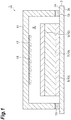
FIG. 1 is a cross-sectional view of a light emitting device according to one embodiment. -
FIG. 2 is a cross-sectional view showing a cathode layer. - Exemplary embodiments of the present invention will be described below in detail with reference to the appended drawings. Here, the same or corresponding components are denoted with the same reference numerals in the following description, and redundant descriptions thereof will be omitted.
- As shown in
FIG. 1 , a light emitting device 1 includes asupport substrate 3, anorganic EL element 10, and asealing member 11. Theorganic EL element 10 includes an anode layer (first electrode layer) 5, an organicfunctional layer 7, and a cathode layer (second electrode layer) 9. - The
support substrate 3 is made of glass or a resin that transmits visible light (light with a wavelength of 400 nm to 800 nm). When resin materials are selected for thesupport substrate 3, for example, polyethersulfone (PES); a polyester resin such as polyethylene terephthalate (PET), and polyethylene naphthalate (PEN); a polyolefin resin such as polyethylene (PE), polypropylene (PP), and a cyclic polyolefin; a polyamide resin; a polycarbonate resin; a polystyrene resin; a polyvinyl alcohol resin; a saponified ethylene-vinyl acetate copolymer product; a polyacrylonitrile resin; an acetal resin; a polyimide resin; or an epoxy resin can be used. - As a material of the
support substrate 3, among the above resins, a polyester resin and a polyolefin resin are preferable and polyethylene terephthalate and polyethylene naphthalate are particularly preferable because they have high heat resistance, a low coefficient of linear expansion, and low production costs. In addition, one of these resins may be used alone or two or more thereof may be used in combination. - A water barrier layer (barrier layer) may be disposed on one
main surface 3a of thesupport substrate 3. The othermain surface 3b of thesupport substrate 3 is a light emitting surface. - The
anode layer 5 is disposed on onemain surface 3a of thesupport substrate 3. As theanode layer 5, an electrode layer exhibiting light transmittance is used. As an electrode (layer) exhibiting light transmittance, a thin film of a metal oxide, a metal sulfide or a metal having high electrical conductivity can be used and a thin film having high light transmittance is suitably used. For example, thin films made of indium oxide, zinc oxide, tin oxide, indium tin oxide (abbreviation ITO), indium zinc oxide (abbreviation IZO), gold, platinum, silver, copper, and the like may be used, and a thin film made of ITO, IZO, or tin oxide among them is suitably used. - As the
anode layer 5, a transparent conductive film of an organic substance such as polyaniline and derivatives thereof, and polythiophene and derivatives thereof may be used. In addition, as theanode layer 5, an electrode in which a metal, a metal alloy, or the like is patterned in a mesh form or an electrode in which nanowires containing silver are formed in a network form may be used. - The thickness of the
anode layer 5 can be determined in consideration of light transmittance, electrical conductivity, and the like. The thickness of theanode layer 5 is generally, 10 nm to 10 µm, preferably 20 nm to 1 µm, and more preferably 50 nm to 500 nm. - Examples of a method of forming the
anode layer 5 include a vacuum deposition method, a sputtering method, an ion plating method, a plating method, and a coating method. - The organic
functional layer 7 is disposed on theanode layer 5. The organicfunctional layer 7 includes a light emitting layer. Generally, the organicfunctional layer 7 includes an organic substance that mainly emits fluorescence and/or phosphorescence or an organic substance and a dopant material for a light emitting layer that assists the organic substance. The dopant material for a light emitting layer is added, for example, in order to improve luminous efficiency and change a light emission wavelength. Here, the organic substance may be a low-molecular-weight compound or a high-molecular-weight compound. Examples of a light emitting material constituting the organicfunctional layer 7 include the following dye materials, metal complex materials, polymer materials, and dopant materials for a light emitting layer. - Examples of the dye material include cyclopentamine and derivatives thereof, tetraphenyl butadiene and derivatives thereof, triphenylamine and derivatives thereof, oxadiazole and derivatives thereof, pyrazoloquinoline and derivatives thereof, distyrylbenzene and derivatives thereof, distyrylarylenes and derivatives thereof, pyrrole and derivatives thereof, thiophene compounds, pyridine compounds, perinone and derivatives thereof, perylene and derivatives thereof, oligothiophenes and derivatives thereof, oxadiazole dimers and derivatives thereof, pyrazoline dimers and derivatives thereof, quinacridone and derivatives thereof, and coumarin and derivatives thereof.
- Examples of the metal complex material include metal complexes including a rare earth metal such as Tb, Eu, and Dy or Al, Zn, Be, Pt, Ir, or the like as a central metal and having an oxadiazole, thiadiazole, phenylpyridine, phenylbenzimidazol, or quinoline structure as a ligand. Examples of the metal complex include a metal complex having luminescence in a triplet excited state of an iridium complex, a platinum complex, or the like, an aluminum quinolinol complex, a benzoquinolinol beryllium complex, a benzoxazolyl zinc complex, a benzothiazole zinc complex, an azomethyl zinc complex, a porphyrin zinc complex, and a phenanthroline europium complex.
- Examples of the polymer material include polyparaphenylene vinylene and derivatives thereof, polythiophene and derivatives thereof, polyparaphenylene and derivatives thereof, polysilane and derivatives thereof, polyacetylene and derivatives thereof, polyfluorene and derivatives thereof, polyvinylcarbazole and derivatives thereof, a dye material, and a material obtained by polymerizing metal complex materials.
- Examples of the dopant material for a light emitting layer include perylene and derivatives thereof, coumarin and derivatives thereof, rubrene and derivatives thereof, quinacridone and derivatives thereof, squarylium and derivatives thereof, porphyrin and derivatives thereof, styryl dyes, tetracene and derivatives thereof, pyrazolone and derivatives thereof, decacyclene and derivatives thereof, and phenoxazone and derivatives thereof.
- The thickness of the organic
functional layer 7 is generally about 2 nm to 200 nm. For example, the organicfunctional layer 7 is formed by a coating method using a coating solution (for example, an ink) containing the light emitting material described above. A solvent of a coating solution containing the light emitting material is not limited as long as it dissolves the light emitting material. - The
cathode layer 9 is disposed on the organicfunctional layer 7. As shown inFIG. 2 , thecathode layer 9 includes a first cathode layer (first metal layer) 9a, a second cathode layer (second metal layer) 9b, a third cathode layer (third metal layer) 9c, and a fourth cathode layer (fourth metal layer) 9d. Thefirst cathode layer 9a is made of aluminum. Thesecond cathode layer 9b is made of silver. Thethird cathode layer 9c is made of aluminum. Thefourth cathode layer 9d is made of silver. - The thickness of the
cathode layer 9 is generally 10 nm to 10 µm, and preferably 100 nm to 1 µm. In the present embodiment, the thickness of thecathode layer 9 is 700 nm. Specifically, the thickness of thefirst cathode layer 9a is, for example, 200 nm. The thickness of thesecond cathode layer 9b is, for example, 100 nm. The thickness of thethird cathode layer 9c is, for example, 300 nm. Thefourth cathode layer 9d is made of silver. The thickness of thefourth cathode layer 9d is, for example, 100 nm. - In the
cathode layer 9, thefirst cathode layer 9a, thesecond cathode layer 9b, thethird cathode layer 9c, and thefourth cathode layer 9d are laminated in that order. Thefirst cathode layer 9a is the lowermost layer of thecathode layer 9. That is, thefirst cathode layer 9a is disposed on the organicfunctional layer 7. Thefourth cathode layer 9d is the uppermost layer of thecathode layer 9. That is, thefourth cathode layer 9d faces the sealingmember 11. - Examples of a method of forming the
cathode layer 9 include a vacuum deposition method, a sputtering method, a lamination method of thermocompression-bonding a metal thin film, and a coating method. - The sealing
member 11 seals theorganic EL element 10. The sealingmember 11 is a box-shaped member. As a material of the sealingmember 11, for example, glass, a metal selected from among aluminum, copper, and iron, and an alloy containing at least one among such metals can be used. The sealingmember 11 is disposed so that it covers theorganic EL element 10 disposed on thesupport substrate 3. The sealingmember 11 is disposed on thesupport substrate 3 and forms a space S in which theorganic EL element 10 is accommodated. An inert gas is contained in the space S. The inert gas is, for example, nitrogen gas. - The sealing
member 11 is adhered to thesupport substrate 3 by anadhesive part 13. Theadhesive part 13 is disposed in a frame form, and adheres thesupport substrate 3 to the sealingmember 11. Thereby, theorganic EL element 10 is sealed and protected from oxygen in the atmosphere and water. For example, theadhesive part 13 is made of a transparent material such as an ultraviolet curable resin, a thermosetting resin, an ultraviolet delayed curable resin, and a 2-liquid mixture curable resin which is formed of an epoxy resin or other resins. - A
desiccant 15 is provided inside the sealingmember 11. Specifically, thedesiccant 15 is disposed on an inner surface (ceiling surface) of the sealingmember 11 that faces thecathode layer 9. In the present embodiment, thedesiccant 15 has a sheet form. In the present embodiment, thedesiccant 15 contains polytetrafluoroethylene, calcium oxide, and carbon. A plurality ofdesiccants 15 may be provided in the sealingmember 11. Thedesiccant 15 is attached to the sealingmember 11 via an adhesive layer (adhesive part) 17. Theadhesive layer 17 contains an acrylic acid ester copolymer. - As described above, in the light emitting device 1 according to the present embodiment, in the sealing
member 11, thedesiccant 15 is provided at a position facing thecathode layer 9. In this configuration, thefourth cathode layer 9d which is the uppermost layer of thecathode layer 9 is made of silver. Thereby, in the light emitting device 1, it is possible to reduce a reaction between a degassing component of thedesiccant 15 and thecathode layer 9. Therefore, in the light emitting device 1, it is possible to reduce the occurrence of unevenness in a light emitting unit (the cathode layer 9). As a result, in the light emitting device 1, it is possible to improve light emission quality. - In the present embodiment, in the
cathode layer 9, on the organicfunctional layer 7, thefirst cathode layer 9a made of aluminum, thesecond cathode layer 9b made of silver, thethird cathode layer 9c made of aluminum, and thefourth cathode layer 9d made of silver are laminated in that order. In such a configuration,_it is possible to further reduce the occurrence of the light emitting unit. - Here, a dark spot (non-light emitting point) is generated in a defective part of the
cathode layer 9, and unevenness (hereinafter referred to as "haze unevenness") in which a plurality of fine dark spots are collected is generated. In the present embodiment, the total thickness of thecathode layer 9 is 700 nm. In addition, in thecathode layer 9, thefirst cathode layer 9a and thethird cathode layer 9c which are made of aluminum, and thesecond cathode layer 9b and thefourth cathode layer 9d which are made of silver are alternately formed. In this manner, when metal layers made of different materials are alternately formed, and thus thecathode layer 9 is formed by, for example, a deposition method, since the ordering of the layers has variation, the rigidity of thecathode layer 9 can be secured. Therefore, it is possible to reduce the occurrence of cracks (breakages) in thecathode layer 9 due to foreign matter and the occurrence of structural defects in thecathode layer 9. As a result, since it is possible to reduce the occurrence of dark spots, it is possible to reduce the occurrence of haze unevenness. In particular, when the total thickness of thecathode layer 9 is set to 500 nm or more, it is possible to effectively reduce the occurrence of dark spots in thecathode layer 9. - In the present embodiment, the
desiccant 15 contains polytetrafluoroethylene, calcium oxide, and carbon. When thedesiccant 15 is used, a configuration of thecathode layer 9 having the above structure is particularly effective in reducing the occurrence of unevenness in the light emitting unit. - In the present embodiment, the
desiccant 15 is attached to the sealingmember 11 via theadhesive layer 17. In the present embodiment, theadhesive layer 17 contains an acrylic acid ester copolymer. There is a possibility of a degassing component being degenerated from theadhesive layer 17 over time. Since thecathode layer 9 serves as thefourth cathode layer 9d that is the uppermost layer, it is possible to reduce a reaction with a degassing component generated from theadhesive layer 17 containing an acrylic acid ester copolymer. Thus, it is possible to reduce the occurrence of unevenness due to the degassing component of thedesiccant 15. - The present invention will be described below in further detail with reference to examples and comparative examples. However, the present invention is not limited to the following examples.
- [Example 1] As Example 1, a light emitting device including an organic EL element in which an anode layer, an organic functional layer, a cathode layer and a sealing layer were laminated on a support substrate in that order was produced.
- As the support substrate, alkali-free glass with a thickness of 0.5 mm was prepared. On the support substrate, the anode layer and the organic functional layer were formed. As the organic functional layer, a hole injection layer, a hole transport layer, a light emitting layer, and an electron injection layer were formed.
- As the cathode layer, four layers of aluminum/silver/aluminum/silver were formed by a vacuum deposition method. The thickness of the cathode layer was 700 nm. Specifically, the thickness of the first aluminum layer (the lowermost layer) was 200 nm. The thickness of the second silver layer was 100 nm. The thickness of the third aluminum layer was 300 nm. The thickness of the fourth silver layer (the uppermost layer) was 100 nm.
- After the cathode layer was formed, the organic EL element was sealed by a sealing member, and a desiccant was provided on a ceiling surface of the sealing member. A desiccant containing polytetrafluoroethylene, calcium oxide, and carbon was used. The desiccant was attached to the sealing member via the adhesive layer. An adhesive layer containing an acrylic acid ester copolymer was used. Thereby, the light emitting device of Example 1 was obtained.
- The light emitting device of Example 1 was left in a temperature of 85 °C and a humidity (RH) of 90% environment, and it was checked whether haze unevenness occurred after 4 days and whether unevenness occurred due to a desiccant during initial light emission (initial). The found results are shown in Table 1. In Table 1, "X" indicates that unevenness occurred, and "O" indicates that no unevenness occurred. Here, when it is shown that unevenness occurred, this means that unevenness occurred to an extent that they affected light emission quality.
[Table 1] Occurrence of haze unevenness Occurrence of unevenness due to desiccant Example 1 ○ ○ Comparative Example 1 X ○ Comparative Example 2 ○ X - As shown in Table 1, in the light emitting device of Example 1, the occurrence of haze unevenness and the occurrence of unevenness due to a desiccant were not found. Haze unevenness was not found even after 10 days.
- In Comparative Example 1, a light emitting device was obtained in the same production method as in Example 1 except that a cathode layer was composed of two layers which were aluminum/silver. The thickness of the cathode layer was 300 nm. Specifically, the thickness of the first aluminum layer (the lowermost layer) was 200 nm. The thickness of the second silver layer (the uppermost layer) was 100 nm. In the light emitting device of Comparative Example 1, since the uppermost layer of the cathode layer was made of silver, the occurrence of unevenness due to a desiccant during initial light emission was not found. Haze unevenness was found after 4 days.
- In Comparative Example 2, a light emitting device was obtained in the same production method as in Example 1 except that a cathode layer was composed of three layers which were aluminum/silver/aluminum. The thickness of the cathode layer was 600 nm. Specifically, the thickness of the first aluminum layer (the lowermost layer) was 200 nm. The thickness of the second silver layer was 100 nm. The thickness of the third aluminum layer (the uppermost layer) was 300 nm. In the light emitting device of Comparative Example 2, since the uppermost layer of the cathode layer was made of aluminum, unevenness due to a desiccant during initial light emission was found. No haze unevenness was found even after 4 days because the thickness of the cathode layer was formed to be relatively high.
- Here, the present invention is not limited to the present embodiment described above, and various modifications can be made. For example, in the above embodiment, the
organic EL element 10 in which the organicfunctional layer 7 including a light emitting layer is disposed between theanode layer 5 and thecathode layer 9 is shown. However, the configuration of the organicfunctional layer 7 is not limited thereto. The organicfunctional layer 7 may have the following configurations. - (a) (Anode layer)/light emitting layer/(cathode layer)
- (b) (Anode layer)/hole injection layer/light emitting layer/(cathode layer)
- (c) (Anode layer)/hole injection layer/light emitting layer/electron injection layer/(cathode layer)
- (d) (Anode layer)/hole injection layer/light emitting layer/electron transport layer/electron injection layer/(cathode layer)
- (e) (Anode layer)/hole injection layer/hole transport layer/light emitting layer/(cathode layer)
- (f) (Anode layer)/hole injection layer/hole transport layer/light emitting layer/electron injection layer/(cathode layer)
- (g) (Anode layer)/hole injection layer/hole transport layer/light emitting layer/electron transport layer/electron injection layer/(cathode layer)
- (h) (Anode layer)/light emitting layer/electron injection layer/(cathode layer)
- (i) (Anode layer)/light emitting layer/electron transport layer/electron injection layer/(cathode layer)
Here, the symbol "/" indicates that layers between which the symbol "/" is interposed are laminated adjacent to each other. The configuration of (a) is a configuration of theorganic EL element 10 in the above embodiment.
As materials of the hole injection layer, the hole transport layer, the electron transport layer and the electron injection layer, known materials can be used. The hole injection layer, the hole transport layer, the electron transport layer and the electron injection layer can be formed by, for example, a coating method in the same manner as in the organicfunctional layer 7.
Theorganic EL element 10 may include a single organicfunctional layer 7 or two or more organicfunctional layers 7. In any one of the layered configurations of (a) to (i), when a lamination structure disposed between theanode layer 5 and thecathode layer 9 is set as a "structural unit A," as a configuration of an organic EL element including two organicfunctional layers 7, for example, a layered configuration shown in the following (j), can be exemplified. Two layered configurations (structural units A) may be the same or different from each other. - (j) Anode layer/(structural unit A)/charge generation layer/(structural unit A)/cathode layer
Here, the charge generation layer is a layer in which holes and electrons are generated when an electric field is applied. As the charge generation layer, a thin film made of, for example, vanadium oxide, ITO, or molybdenum oxide, can be exemplified.
In addition, when "(structural unit A)/charge generation layer" is set as a "structural unit B," as a configuration of an organic EL element including three or more organicfunctional layers 7, for example, a layered configuration shown in the following (k), can be exemplified. - (k) Anode layer/(structural unit B)x/(structural unit A)/cathode layer
- The symbol "x" represents an integer of 2 or more, and "(structural unit B)x" represents a laminate in which x (structural units B) are laminated. In addition, layered configurations of a plurality of (structural units B) may be the same or different from each other.
- An organic EL element in which a plurality of organic
functional layers 7 are directly laminated without providing a charge generation layer may be formed. - An example in which the
cathode layer 9 is composed of four layers including thefirst cathode layer 9a, thesecond cathode layer 9b, thethird cathode layer 9c, and thefourth cathode layer 9d has been described in the above embodiment. However, thecathode layer 9 may be composed of at least three metal layers. In the case of three layers, the cathode layer is preferably composed of silver/aluminum/silver layers. -
- 1 Light emitting device
- 3 Support substrate
- 5 Anode layer (first electrode layer)
- 7 Organic functional layer
- 9 Cathode layer (second electrode layer)
- 9a First cathode layer (first metal layer)
- 9b Second cathode layer (second metal layer)
- 9c Third cathode layer (third metal layer)
- 9d Fourth cathode layer (fourth metal layer)
- 10 Organic EL element
- 11 Sealing member
- 15 Desiccant
- 17 Adhesive layer (adhesive part)
- S Space
Claims (4)
- A light emitting device including a support substrate, an organic EL element disposed on the support substrate, and a sealing member that seals the organic EL element and has a space in which the organic EL element is accommodated, and an inert gas is contained in the space,
wherein the organic EL element is formed by laminating a first electrode layer, an organic functional layer and a second electrode layer on the support substrate in that order,
in the sealing member, a desiccant is provided at a position facing the second electrode layer,
the second electrode layer includes at least three metal layers, and
among the plurality of metal layers, at least one of the metal layers is made of aluminum and the uppermost metal layer is made of silver. - The light emitting device according to Claim 1 ,
wherein, in the second electrode layer, a first metal layer made of aluminum, a second metal layer made of silver, a third metal layer made of aluminum, and a fourth metal layer made of silver are laminated on the organic functional layer in that order. - The light emitting device according to Claim 1 or 2,
wherein the desiccant contains at least one selected from the group consisting of polytetrafluoroethylene, calcium oxide, and carbon. - The light emitting device according to any one of Claims 1 to 3,
wherein the desiccant is attached to the sealing member via an adhesive part, and
the adhesive part contains an acrylic acid ester copolymer.
Applications Claiming Priority (2)
| Application Number | Priority Date | Filing Date | Title |
|---|---|---|---|
| JP2016012544A JP6655403B2 (en) | 2016-01-26 | 2016-01-26 | Light emitting device |
| PCT/JP2016/087560 WO2017130600A1 (en) | 2016-01-26 | 2016-12-16 | Light-emitting device |
Publications (2)
| Publication Number | Publication Date |
|---|---|
| EP3410823A1 true EP3410823A1 (en) | 2018-12-05 |
| EP3410823A4 EP3410823A4 (en) | 2019-10-23 |
Family
ID=59397658
Family Applications (1)
| Application Number | Title | Priority Date | Filing Date |
|---|---|---|---|
| EP16888184.5A Withdrawn EP3410823A4 (en) | 2016-01-26 | 2016-12-16 | Light-emitting device |
Country Status (6)
| Country | Link |
|---|---|
| US (1) | US20190036079A1 (en) |
| EP (1) | EP3410823A4 (en) |
| JP (1) | JP6655403B2 (en) |
| KR (1) | KR20180105162A (en) |
| CN (1) | CN108605392A (en) |
| WO (1) | WO2017130600A1 (en) |
Family Cites Families (14)
| Publication number | Priority date | Publication date | Assignee | Title |
|---|---|---|---|---|
| JP2001035659A (en) * | 1999-07-15 | 2001-02-09 | Nec Corp | Organic electroluminescent device and method of manufacturing the same |
| KR100844803B1 (en) * | 2002-11-19 | 2008-07-07 | 엘지디스플레이 주식회사 | Organic light emitting diode |
| WO2006016153A1 (en) * | 2004-08-10 | 2006-02-16 | Cambridge Display Technology Limited | Light emissive device |
| JP2006059668A (en) * | 2004-08-20 | 2006-03-02 | Seiko Epson Corp | ORGANIC ELECTROLUMINESCENT DEVICE, METHOD FOR PRODUCING ORGANIC ELECTROLUMINESCENT DEVICE, AND ELECTRONIC DEVICE |
| JP2006228519A (en) * | 2005-02-16 | 2006-08-31 | Canon Inc | Organic electroluminescence device and method for manufacturing the same |
| JP2007250459A (en) * | 2006-03-17 | 2007-09-27 | Sanyo Electric Co Ltd | Electroluminescent display and manufacturing method thereof |
| WO2008081593A1 (en) * | 2006-12-28 | 2008-07-10 | Zeon Corporation | Laminated body for light emitting element, and light emitting element |
| JP5231774B2 (en) * | 2007-09-07 | 2013-07-10 | リンテック株式会社 | Double-sided adhesive sheet |
| JP2010123439A (en) * | 2008-11-20 | 2010-06-03 | Fujifilm Corp | Organic electroluminescent element |
| US20120074398A1 (en) * | 2009-07-01 | 2012-03-29 | Sharp Kabushiki Kaisha | Organic el illuminant, organic el illuminating device, and method for fabricating organic el illuminant |
| JP2013214369A (en) * | 2012-03-30 | 2013-10-17 | Furukawa Electric Co Ltd:The | Resin composition for organic electroluminescent element sealing, adhesive film and gas-barrier film, each arranged with resin composition, organic electroluminescent element, and organic electroluminescent panel |
| GB2516607A (en) * | 2013-03-06 | 2015-02-04 | Cambridge Display Tech Ltd | Organic electronic device |
| CN203596354U (en) * | 2013-10-30 | 2014-05-14 | 上海大学 | Organic electroluminescence diode parallel connected structure mode composite lighting device |
| JP2015162444A (en) * | 2014-02-28 | 2015-09-07 | パイオニア株式会社 | light-emitting device |
-
2016
- 2016-01-26 JP JP2016012544A patent/JP6655403B2/en not_active Expired - Fee Related
- 2016-12-16 WO PCT/JP2016/087560 patent/WO2017130600A1/en not_active Ceased
- 2016-12-16 KR KR1020187022803A patent/KR20180105162A/en not_active Withdrawn
- 2016-12-16 US US16/072,256 patent/US20190036079A1/en not_active Abandoned
- 2016-12-16 EP EP16888184.5A patent/EP3410823A4/en not_active Withdrawn
- 2016-12-16 CN CN201680080093.0A patent/CN108605392A/en active Pending
Also Published As
| Publication number | Publication date |
|---|---|
| JP6655403B2 (en) | 2020-02-26 |
| KR20180105162A (en) | 2018-09-27 |
| CN108605392A (en) | 2018-09-28 |
| WO2017130600A1 (en) | 2017-08-03 |
| EP3410823A4 (en) | 2019-10-23 |
| US20190036079A1 (en) | 2019-01-31 |
| JP2017134942A (en) | 2017-08-03 |
Similar Documents
| Publication | Publication Date | Title |
|---|---|---|
| TWI523295B (en) | Organic light-emitting device comprising flexible substrate and preparation method thereof | |
| JP2000260572A (en) | Organic electroluminescence panel | |
| KR101866296B1 (en) | Organic light emitting device and method for preparing the same | |
| JP5729749B2 (en) | Method for manufacturing organic electroluminescence element | |
| WO2012070574A1 (en) | Light emitting device and method for producing light emitting device | |
| WO2015107604A1 (en) | Light emitting apparatus and light emitting apparatus manufacturing method | |
| EP3410823A1 (en) | Light-emitting device | |
| US10991905B2 (en) | Organic electroluminescent element | |
| JP6284670B1 (en) | Manufacturing method of organic device | |
| US20200099016A1 (en) | Method for manufacturing organic device | |
| JP2006286242A (en) | Flexible organic electroluminescence device | |
| US20200388786A1 (en) | Electronic device manufacturing method | |
| JP2017162770A (en) | Manufacturing method of organic el lighting and inspection panel | |
| US10403858B2 (en) | Method for manufacturing organic electronic device and method for manufacturing sealing member | |
| US20200266247A1 (en) | Mother board, and method for manufacturing lighting device | |
| KR20150037025A (en) | Organic light emitting device comprising flexible substrate and method for preparing thereof | |
| JP2017068979A (en) | Flexible organic el device and method for manufacturing the same | |
| WO2017212890A1 (en) | Method for manufacturing organic device | |
| KR20150122856A (en) | Method of encapsulating oled | |
| KR20150035262A (en) | Organic light emitting device and method for preparing thereof |
Legal Events
| Date | Code | Title | Description |
|---|---|---|---|
| STAA | Information on the status of an ep patent application or granted ep patent |
Free format text: STATUS: THE INTERNATIONAL PUBLICATION HAS BEEN MADE |
|
| PUAI | Public reference made under article 153(3) epc to a published international application that has entered the european phase |
Free format text: ORIGINAL CODE: 0009012 |
|
| STAA | Information on the status of an ep patent application or granted ep patent |
Free format text: STATUS: REQUEST FOR EXAMINATION WAS MADE |
|
| 17P | Request for examination filed |
Effective date: 20180718 |
|
| AK | Designated contracting states |
Kind code of ref document: A1 Designated state(s): AL AT BE BG CH CY CZ DE DK EE ES FI FR GB GR HR HU IE IS IT LI LT LU LV MC MK MT NL NO PL PT RO RS SE SI SK SM TR |
|
| AX | Request for extension of the european patent |
Extension state: BA ME |
|
| DAV | Request for validation of the european patent (deleted) | ||
| DAX | Request for extension of the european patent (deleted) | ||
| A4 | Supplementary search report drawn up and despatched |
Effective date: 20190923 |
|
| RIC1 | Information provided on ipc code assigned before grant |
Ipc: H05B 33/26 20060101ALI20190917BHEP Ipc: H05B 33/04 20060101AFI20190917BHEP Ipc: H01L 51/50 20060101ALI20190917BHEP |
|
| STAA | Information on the status of an ep patent application or granted ep patent |
Free format text: STATUS: THE APPLICATION HAS BEEN WITHDRAWN |
|
| 18W | Application withdrawn |
Effective date: 20200408 |