EP3410159A2 - Light detection device and operating method thereof - Google Patents
Light detection device and operating method thereof Download PDFInfo
- Publication number
- EP3410159A2 EP3410159A2 EP18169763.2A EP18169763A EP3410159A2 EP 3410159 A2 EP3410159 A2 EP 3410159A2 EP 18169763 A EP18169763 A EP 18169763A EP 3410159 A2 EP3410159 A2 EP 3410159A2
- Authority
- EP
- European Patent Office
- Prior art keywords
- light
- detection device
- light detection
- image data
- source module
- Prior art date
- Legal status (The legal status is an assumption and is not a legal conclusion. Google has not performed a legal analysis and makes no representation as to the accuracy of the status listed.)
- Granted
Links
Images




Classifications
-
- H—ELECTRICITY
- H10—SEMICONDUCTOR DEVICES; ELECTRIC SOLID-STATE DEVICES NOT OTHERWISE PROVIDED FOR
- H10F—INORGANIC SEMICONDUCTOR DEVICES SENSITIVE TO INFRARED RADIATION, LIGHT, ELECTROMAGNETIC RADIATION OF SHORTER WAVELENGTH OR CORPUSCULAR RADIATION
- H10F39/00—Integrated devices, or assemblies of multiple devices, comprising at least one element covered by group H10F30/00, e.g. radiation detectors comprising photodiode arrays
- H10F39/10—Integrated devices
- H10F39/12—Image sensors
- H10F39/18—Complementary metal-oxide-semiconductor [CMOS] image sensors; Photodiode array image sensors
- H10F39/189—X-ray, gamma-ray or corpuscular radiation imagers
- H10F39/1898—Indirect radiation image sensors, e.g. using luminescent members
-
- G—PHYSICS
- G01—MEASURING; TESTING
- G01N—INVESTIGATING OR ANALYSING MATERIALS BY DETERMINING THEIR CHEMICAL OR PHYSICAL PROPERTIES
- G01N23/00—Investigating or analysing materials by the use of wave or particle radiation, e.g. X-rays or neutrons, not covered by groups G01N3/00 – G01N17/00, G01N21/00 or G01N22/00
- G01N23/02—Investigating or analysing materials by the use of wave or particle radiation, e.g. X-rays or neutrons, not covered by groups G01N3/00 – G01N17/00, G01N21/00 or G01N22/00 by transmitting the radiation through the material
- G01N23/04—Investigating or analysing materials by the use of wave or particle radiation, e.g. X-rays or neutrons, not covered by groups G01N3/00 – G01N17/00, G01N21/00 or G01N22/00 by transmitting the radiation through the material and forming images of the material
-
- G—PHYSICS
- G01—MEASURING; TESTING
- G01T—MEASUREMENT OF NUCLEAR OR X-RADIATION
- G01T1/00—Measuring X-radiation, gamma radiation, corpuscular radiation, or cosmic radiation
- G01T1/16—Measuring radiation intensity
- G01T1/20—Measuring radiation intensity with scintillation detectors
-
- G—PHYSICS
- G01—MEASURING; TESTING
- G01T—MEASUREMENT OF NUCLEAR OR X-RADIATION
- G01T1/00—Measuring X-radiation, gamma radiation, corpuscular radiation, or cosmic radiation
- G01T1/16—Measuring radiation intensity
- G01T1/20—Measuring radiation intensity with scintillation detectors
- G01T1/2018—Scintillation-photodiode combinations
- G01T1/20188—Auxiliary details, e.g. casings or cooling
-
- H—ELECTRICITY
- H04—ELECTRIC COMMUNICATION TECHNIQUE
- H04N—PICTORIAL COMMUNICATION, e.g. TELEVISION
- H04N23/00—Cameras or camera modules comprising electronic image sensors; Control thereof
- H04N23/30—Cameras or camera modules comprising electronic image sensors; Control thereof for generating image signals from X-rays
Definitions
- This disclosure generally related to a light detection device and an operation method thereof according to the pre-characterizing clauses of claims 1 and 6.
- Light sensing technology has been applied in many electronic products and detection equipment with the related development, and the light sensing technology capable of detecting X-ray is one of the applications that has received considerable attention. Because of properties such as low irradiation dose, fast electronic imaging, and convenience of viewing, copying, capturing, transferring, and analyzing electronic images, the traditional approach using films for detecting X-ray has been gradually replaced by the digital detection device, and the digital detection device has become the current trend of development of digital medical imaging. Photo diodes are generally used as light sensing units in the digital light detection device for detecting X-ray energy.
- the present disclosure aims at providing a light detection device and an operation method thereof.
- a light source module is disposed in the light detection device, and the light source module is used to perform a self-detection for determining whether the light detection device is normal or not. Detection errors generated by the abnormal light detection device and the related problems may be avoided accordingly.
- the claimed light detection device includes a housing, a sensing substrate, a scintillator layer, and a light source module.
- the sensing substrate is disposed inside the housing.
- the scintillator layer is disposed inside the housing and disposed above the sensing substrate.
- the light source module is at least partially disposed inside the housing.
- the claimed operating method of a light detection device includes the following steps.
- a light detection device is provided.
- the light detection device includes a housing, a sensing substrate, a scintillator layer, and a light source module.
- the sensing substrate is disposed inside the housing.
- the scintillator layer is disposed inside the housing and disposed above the sensing substrate.
- the light source module is at least partially disposed inside the housing.
- the light detection device is turned on and first image data is captured. Subsequently, the light source module is turned on and second image data is captured. The first image data is compared with the second image data for determining a condition of the light detection device.
- FIG. 1 is a cross-sectional schematic drawing illustrating a light detection device according to a first embodiment of the present disclosure
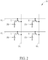
- FIG. 2 is a schematic circuit diagram of a part of a sensing substrate in this embodiment.
- a light detection device 101 is provided in this embodiment.
- the light detection device 101 includes a housing 10, a sensing substrate 30, a scintillator layer 40, and a light source module 50.
- the sensing substrate 30 and the scintillator layer 40 are disposed inside the housing 10.
- the scintillator layer 40 is disposed above the sensing substrate 30, and the light source module 50 is at least partially disposed inside the housing 10.
- the portion of the light source module 50 disposed inside the housing has to be capable of emitting light.
- the light detection device 101 may be used to sense detection light 90 and generated corresponding image data, and the detection light 90 may include an X-ray or light within other suitable wavelength ranges, such as a gamma ray (y ray).
- the light source module 50 is used to provide light to the sensing substrate 30 during a self-detection. Therefore, in some embodiments, the light source module 30 may be disposed completely inside the housing 10, or the light source module 30 may be partly disposed inside the housing 10 and provide light required in the self-detection.
- the housing 10 may be made of an opaque material for blocking visible light or light within other wavelength range from entering the housing 10, but not limited thereto.
- the scintillator layer 40 is used to convert light within a specific wavelength range (such as an X-ray) into visible light, and the material of the scintillator layer 40 may include cesium iodide (CsI), but not limited thereto.
- the sensing substrate 30 may include a plurality of switching units T and a plurality of light sensing units PD, and each of the light sensing units PD is electrically connected with at least one of the switching units T.
- the sensing substrate 30 may include a plurality of data lines DL and a plurality of gate lines GL interlaced with one another for forming an array.
- Each of the switching units T may include a transistor electrically connected with a corresponding data line DL and a corresponding gate line GL
- the light sensing unit PD may include a photodiode coupled with a corresponding switching unit T.
- a semiconductor material in the transistor of the switching unit T may be low temperature poly-silicon (LTPS), indium gallium zinc oxide (IGZO), or amorphous silicon (a-Si), but not limited thereto.
- the switching condition of the switching unit T may be controlled via the gate line GL, a signal generated from the light sensing unit PD may be received via the data line DL when the corresponding switching unit T is turned on, and each of the light sensing units PD and the corresponding switching unit T may be regarded as one pixel, but not limited thereto.
- the sensing substrate 30 in the light detection device of the present disclosure is not limited to the conditions described above, and other suitable kinds of sensing substrates may also be applied in the present disclosure.
- the light detection device 101 may further include a support substrate 20 disposed inside the housing 10, and the sensing substrate 30, the scintillator layer 40, and the light source module 50 may be disposed on the support substrate 20, but not limited thereto. Additionally, in some embodiments, the light source module 50 may be disposed under the sensing substrate 30, and the sensing substrate 30 may be disposed between the scintillator layer 40 and the light source module 50 in a top view (projective) direction Z perpendicular to the sensing substrate 30, but not limited thereto.
- the light source module 50 may be disposed between the support substrate 20 and the sensing substrate 30, and the scintillator layer 40 and the light source module 50 may be disposed at a top side and a bottom side of the sensing substrate 30 respectively in the top view direction Z. Accordingly, the light source module 50 may provide light to the sensing substrate 30 from the bottom side of the sensing substrate 30 for performing the self-detection. Additionally, in some embodiments, the light source module 50 may include an edge type light source module or a direct type light source module.
- the light source module 50 may include a light source 51 (such as a light emitting diode, LED or OLED) and a light guide plate 52 disposed adjacent to each other.
- a light source 51 such as a light emitting diode, LED or OLED
- Light generated by the light source 51 enters the light guide plate 52 from a light incident surface of the light guide plate 52 and are uniformly emitted from an illuminant surface facing the sensing substrate 30.
- a normal direction of the incident surface is perpendicular to the top view direction Z, and a normal direction of the illuminant surface is parallel with the top view direction Z.
- the light source module 59 may be electrically connected to a circuit board 60 disposed at a back side of the support substrate 20, and the circuit board 60 may be used to control the switching condition and the light intensity of the light source module 50, but not limited thereto.
- the light source module 50 may include a visible light source module configured to provide visible light irradiating the sensing substrate 30, but not limited thereto.
- the wavelength range of the light emitted from the light source module 50 may be modified to be corresponding to the wavelength range of the light which can be inspected by the sensing substrate 30.
- the light source module 50 may be an infrared light source module or a light source module within other suitable wavelength ranges.
- the light detection device 101 may further include a light filter layer 70 disposed above the scintillator layer 40.
- the visible light may be blocked by the light filter layer 70, and the X-rays (i.e. the detection light 90) may pass through the light filter layer 70, and the material of the light filter layer 70 may include carbon fiber, but not limited thereto.
- the material of the housing 10 may be carbon fiber for blocking the visible light and permitting the X-rays to pass through, but the present disclosure is not limited to this and other appropriate materials may also be used to form the housing 10 and/or the light filter layer 70.
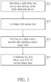
- FIG. 3 is a flow chart of an operation method of the light detection device 101 in this embodiment
- FIG. 4 is a schematic drawing illustrating first image data according to an embodiment of the present disclosure
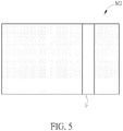
- FIG. 5 is a schematic drawing illustrating second image data according to an embodiment of the present disclosure.
- an operation method of the light detection device 101 is provided in this embodiment, and the operation method includes the following steps. Firstly, in step S11, the light detection device 101 is provided and the light detection device 101 is turned on. In step S12, first image data M1 is captured. Subsequently, in step S13, the light source module 50 is turned on, and second image data M2 is captured.
- step S14 the first image data M1 is compared with the second image data M2 for determining a condition of the light detection device 101 and determining whether the condition of the light detection device 101 is normal or abnormal.
- the sensing substrate 30 is turned on, and the light source module 50 is turned off.
- the first image data M1 is captured under the condition where the light source module 50 is turned off, and the first image data M1 may be regarded as a black screen image.
- the second image data M2 is captured in the condition where the light source module 50 is turned on, and the second image data M2 is an image data obtained after the light emitted from the light source module 50 is received by the sensing substrate 30.
- the above-mentioned steps S11-S14 may be regarded as a self-detection flow performed on the light detection device 101 for confirming whether the light detection device 101 is normal before a step of performing a regular detection by the light detection device 101. Detection errors generated by the light detection device 101 in the regular detection when the light detection device is abnormal and other related problems may be avoided accordingly. Therefore, the light detection device 101 is not irradiated by the detection light 90 in the above-mentioned steps S11-S14, and the abnormal conditions described above may include abnormal conditions related to circuits and/or pixels in the sensing substrate 30 (such as a broken conductive line or a defective pixel), foreign bodies entering the housing 10, and other possible abnormal conditions.
- an abnormal region F may be observed in the second image data M2, and the abnormal region F may be generated by the abnormal conditions related to the circuits and/or the pixels in the sensing substrate 30. Therefore, the light detection device 101 may be determined to be abnormal by the condition of the second image data M2 shown in FIG. 5 and the regular X-ray detection cannot be performed by the light detection device 101.
- the light detection device 101 may be determined to be normal and can be used to perform the X-ray detection, or the light detection device 101 may be determined to be abnormal and the detection should be terminated.
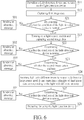
- FIG. 6 is a flow chart of an operation method of a light detection device according to a second embodiment of the present disclosure.
- the difference between the operation method in this embodiment and the operation method in the first embodiment mentioned above is that the operation method of the light detection device in this embodiment may further include step S21 performed after the step S12 and before the step S13.
- the condition of the first image data may be used alone to determine whether the condition of the light detection device 101 is normal or abnormal. The intensity should be uniform on the first image data ideally because the first image data is captured under the condition where the light detection device is not irradiated by the detection light 90 and the light source module 50 is turned off.
- the light detection device 101 may be determined to be abnormal and step S91 may be carried out to sending an abnormal message from the light detection device 101.
- the abnormal message may include a voice, an indication lamp, or text on a display panel for passing the abnormal information, but not limited thereto.
- step S13 if the condition of the light detection device 101 is determined to be normal, step S13 may be carried out to turn on the light source module 50 and capture the second image data.
- step S22 is carried out to compare the first image data with the second image data for determining whether there is dot abnormal region, a linear abnormal region, or a bulk abnormal region and whether it is necessary to carry out step S92 for sending the abnormal message. Additionally, if the light detection device 101 is determined to be normal at the step S22, step S23 may be carried out to determine whether the second image data is uniform or not and confirm whether it is necessary to carry out step S93 for sending the abnormal message.
- FIG. 7 is a schematic drawing illustrating a comparison between third image data captured respectively under light with different intensity emitted from the light source module 50 in the operation method of the light detection device according to this embodiment.
- step S24 may be carried out to emit light with different intensity (or may be regarded as luminance) respectively from the light source module 50 and capture a plurality of third image data corresponding to the light with different intensity for determining whether the condition of the light detection device 101 is normal or abnormal in step S25.
- the light source module 50 may emit light with first intensity P1, light with second intensity P2, light with third intensity P3, and light with fourth intensity respectively, and a plurality of third image data may be captured corresponding to the light with different intensity.
- the third image data may be used to construct the distribution of the image data under light with different intensity.
- a first relation line L1 and a second relation line L2 shown in FIG. 7 may be regarded as normal performance of the pixels in the sensing substrate 30, and the corresponding image data may be saturated when the intensity of light is higher than an upper limit. It is worth noting that the intensity of the image data shown in FIG.
- a third relation line L3 and a fourth relation line L4 shown in FIG. 7 may be relation lines generated from the third image data captured by different pixels in the sensing substrate 30 under the irradiation of the light with the first intensity P1, the light with second intensity P2, the light with the third intensity P3, and the light with the fourth intensity P4.
- step S94 may be carried out to send the abnormal message.
- step S26 may be carried out to prepare for using the light detection device 101.
- the light detection device 101 may be used to perform the regular detection (such as the X-ray detection).
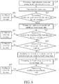
- FIG. 8 is a flow chart of an operation method of a light detection device according to a third embodiment of the present disclosure.
- the difference between the operation method in this embodiment and the operation method in the second embodiment mentioned above is that the operation method of the light detection device in this embodiment may further include step S31 performed after the step S23 for irradiating the light detection device 101 with the detection light 90 and capturing fourth image data.
- step S32 the fourth image data is compared with the second image data for determining whether there is a foreign body on the light detection device 101 and/or whether there is a foreign body in the light detection device 101 in step S33.
- step S95 may be carried out to send the abnormal massage. Additionally, the result of the comparison between the fourth image data and the second image data may also be used to determine whether the material of the scintillator layer 40 is deteriorated for avoiding the influence of the material deterioration of the scintillator layer 40 on the detection results.
- FIG. 9 is a cross-sectional schematic drawing illustrating a light detection device 102 according to a fourth embodiment of the present disclosure.
- the difference between the light detection device 102 and the light detection device in the first embodiment described above is that, in the light detection device 102, the light source module 50 may be disposed above the scintillator layer 40, and the scintillator layer 40 may be disposed between the light source module 50 and the sensing substrate 30.
- the light source module 50 may be disposed between the scintillator layer 40 and the light filter layer 70 in the top view direction Z, and the light source module 50 under this condition may be an edge type light source module for avoiding the influence on the regular light detection and the detection results thereof.
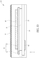
- FIG. 10 is a cross-sectional schematic drawing illustrating a light detection device 103 according to a fifth embodiment of the present disclosure.
- the difference between the light detection device 103 and the light detection device in the first embodiment described above is that, in the light detection device 103, the light source module 50 may be disposed between the scintillator layer 40 and the sensing substrate 30, and the light source module 50 under this condition may be an edge type light source module for avoiding the influence on the regular light detection and the detection results thereof.
- the light source module 50 may also be disposed at other position in the light detection device, such as a corner, a lateral side, or a bottom of the housing, or a part of the light source module 50 may be disposed outside the housing as long as the light provided by the light source module 50 can irradiate the sensing substrate 30.
- the light source module at least partially disposed inside the housing may be used to perform the self-detection for confirming whether the condition of the light detection device is normal or abnormal before performing the regular detection by the light detection device.
- the detection errors generated by the abnormal light detection device in the regular detection and the related problems may be avoided accordingly.
Landscapes
- Health & Medical Sciences (AREA)
- General Physics & Mathematics (AREA)
- Life Sciences & Earth Sciences (AREA)
- Physics & Mathematics (AREA)
- Molecular Biology (AREA)
- High Energy & Nuclear Physics (AREA)
- Spectroscopy & Molecular Physics (AREA)
- Signal Processing (AREA)
- Multimedia (AREA)
- Engineering & Computer Science (AREA)
- Analytical Chemistry (AREA)
- Chemical & Material Sciences (AREA)
- Biochemistry (AREA)
- General Health & Medical Sciences (AREA)
- Immunology (AREA)
- Pathology (AREA)
- Measurement Of Radiation (AREA)
- Geophysics And Detection Of Objects (AREA)
Abstract
Description
- This disclosure generally related to a light detection device and an operation method thereof according to the pre-characterizing clauses of claims 1 and 6.
- Light sensing technology has been applied in many electronic products and detection equipment with the related development, and the light sensing technology capable of detecting X-ray is one of the applications that has received considerable attention. Because of properties such as low irradiation dose, fast electronic imaging, and convenience of viewing, copying, capturing, transferring, and analyzing electronic images, the traditional approach using films for detecting X-ray has been gradually replaced by the digital detection device, and the digital detection device has become the current trend of development of digital medical imaging. Photo diodes are generally used as light sensing units in the digital light detection device for detecting X-ray energy. However, when the light detection device is found to be abnormal after one X-ray irradiation to a human, there has to be a certain time interval between this X-ray irradiation and the next X-ray irradiation because X-rays have a certain degree of harm to humans and have a cumulative effect. It is inconvenient for the examinee and medical disputes may be generated accordingly.
- The present disclosure aims at providing a light detection device and an operation method thereof. A light source module is disposed in the light detection device, and the light source module is used to perform a self-detection for determining whether the light detection device is normal or not. Detection errors generated by the abnormal light detection device and the related problems may be avoided accordingly.
- This is achieved by a light detection device and an operation method thereof according to the pre-characterizing clauses of claims 1 and 6. The dependent claims pertain to corresponding further developments and improvements.
- As will be seen more clearly from the detailed description following below, the claimed light detection device includes a housing, a sensing substrate, a scintillator layer, and a light source module. The sensing substrate is disposed inside the housing. The scintillator layer is disposed inside the housing and disposed above the sensing substrate. The light source module is at least partially disposed inside the housing.
- As will be seen more clearly from the detailed description following below, the claimed operating method of a light detection device includes the following steps. A light detection device is provided. The light detection device includes a housing, a sensing substrate, a scintillator layer, and a light source module. The sensing substrate is disposed inside the housing. The scintillator layer is disposed inside the housing and disposed above the sensing substrate. The light source module is at least partially disposed inside the housing. The light detection device is turned on and first image data is captured. Subsequently, the light source module is turned on and second image data is captured. The first image data is compared with the second image data for determining a condition of the light detection device.
- These and other objectives of the present disclosure will no doubt become clear to those of ordinary skill in the art after reading the following detailed description of the preferred embodiment that is illustrated in the various figures and drawings.
- The disclosure is further illustrated by way of example, taking reference to the accompanying drawings. Thereof
-
FIG. 1 is a cross-sectional schematic drawing illustrating a light detection device according to a first embodiment of the present disclosure, -
FIG. 2 is a schematic circuit diagram of a part of a sensing substrate according to the first embodiment of the present disclosure, -
FIG. 3 is a flow chart of an operation method of the light detection device according to the first embodiment of the present disclosure, -
FIG. 4 is a schematic drawing illustrating first image data according to an embodiment of the present disclosure, -
FIG. 5 is a schematic drawing illustrating second image data according to an embodiment of the present disclosure, -
FIG. 6 is a flow chart of an operation method of a light detection device according to a second embodiment of the present disclosure, -
FIG. 7 is a schematic drawing illustrating a comparison between third image data captured respectively under light with different intensity emitted from a light source module according to the operation method of the light detection device in the second embodiment of the present disclosure, -
FIG. 8 is a flow chart of an operation method of a light detection device according to a third embodiment of the present disclosure, -
FIG. 9 is a cross-sectional schematic drawing illustrating a light detection device according to a fourth embodiment of the present disclosure, and -
FIG. 10 is a cross-sectional schematic drawing illustrating a light detection device according to a fifth embodiment of the present disclosure. -
FIG. 1 is a cross-sectional schematic drawing illustrating a light detection device according to a first embodiment of the present disclosure, andFIG. 2 is a schematic circuit diagram of a part of a sensing substrate in this embodiment. Please note that the figures are only for illustration and the figures may not be to scale. The scale may be further modified according to different design considerations. As shown inFIG. 1 , alight detection device 101 is provided in this embodiment. Thelight detection device 101 includes ahousing 10, asensing substrate 30, ascintillator layer 40, and alight source module 50. Thesensing substrate 30 and thescintillator layer 40 are disposed inside thehousing 10. Thescintillator layer 40 is disposed above thesensing substrate 30, and thelight source module 50 is at least partially disposed inside thehousing 10. The portion of thelight source module 50 disposed inside the housing has to be capable of emitting light. Thelight detection device 101 may be used to sensedetection light 90 and generated corresponding image data, and thedetection light 90 may include an X-ray or light within other suitable wavelength ranges, such as a gamma ray (y ray). Thelight source module 50 is used to provide light to thesensing substrate 30 during a self-detection. Therefore, in some embodiments, thelight source module 30 may be disposed completely inside thehousing 10, or thelight source module 30 may be partly disposed inside thehousing 10 and provide light required in the self-detection. In some embodiments, thehousing 10 may be made of an opaque material for blocking visible light or light within other wavelength range from entering thehousing 10, but not limited thereto. In addition, thescintillator layer 40 is used to convert light within a specific wavelength range (such as an X-ray) into visible light, and the material of thescintillator layer 40 may include cesium iodide (CsI), but not limited thereto. - As shown in
FIG. 1 andFIG. 2 , in some embodiments, thesensing substrate 30 may include a plurality of switching units T and a plurality of light sensing units PD, and each of the light sensing units PD is electrically connected with at least one of the switching units T. For example, thesensing substrate 30 may include a plurality of data lines DL and a plurality of gate lines GL interlaced with one another for forming an array. Each of the switching units T may include a transistor electrically connected with a corresponding data line DL and a corresponding gate line GL, and the light sensing unit PD may include a photodiode coupled with a corresponding switching unit T. A semiconductor material in the transistor of the switching unit T may be low temperature poly-silicon (LTPS), indium gallium zinc oxide (IGZO), or amorphous silicon (a-Si), but not limited thereto. The switching condition of the switching unit T may be controlled via the gate line GL, a signal generated from the light sensing unit PD may be received via the data line DL when the corresponding switching unit T is turned on, and each of the light sensing units PD and the corresponding switching unit T may be regarded as one pixel, but not limited thereto. It is worth noting that thesensing substrate 30 in the light detection device of the present disclosure is not limited to the conditions described above, and other suitable kinds of sensing substrates may also be applied in the present disclosure. - As shown in
FIG. 1 , thelight detection device 101 may further include asupport substrate 20 disposed inside thehousing 10, and thesensing substrate 30, thescintillator layer 40, and thelight source module 50 may be disposed on thesupport substrate 20, but not limited thereto. Additionally, in some embodiments, thelight source module 50 may be disposed under thesensing substrate 30, and thesensing substrate 30 may be disposed between thescintillator layer 40 and thelight source module 50 in a top view (projective) direction Z perpendicular to thesensing substrate 30, but not limited thereto. In other words, thelight source module 50 may be disposed between thesupport substrate 20 and thesensing substrate 30, and thescintillator layer 40 and thelight source module 50 may be disposed at a top side and a bottom side of thesensing substrate 30 respectively in the top view direction Z. Accordingly, thelight source module 50 may provide light to thesensing substrate 30 from the bottom side of thesensing substrate 30 for performing the self-detection. Additionally, in some embodiments, thelight source module 50 may include an edge type light source module or a direct type light source module. For example, when thelight source module 50 is an edge type light source module, thelight source module 50 may include a light source 51 (such as a light emitting diode, LED or OLED) and alight guide plate 52 disposed adjacent to each other. Light generated by thelight source 51 enters thelight guide plate 52 from a light incident surface of thelight guide plate 52 and are uniformly emitted from an illuminant surface facing thesensing substrate 30. A normal direction of the incident surface is perpendicular to the top view direction Z, and a normal direction of the illuminant surface is parallel with the top view direction Z. Additionally, the light source module 59 may be electrically connected to acircuit board 60 disposed at a back side of thesupport substrate 20, and thecircuit board 60 may be used to control the switching condition and the light intensity of thelight source module 50, but not limited thereto. In some embodiments, thelight source module 50 may include a visible light source module configured to provide visible light irradiating thesensing substrate 30, but not limited thereto. In some embodiments, the wavelength range of the light emitted from thelight source module 50 may be modified to be corresponding to the wavelength range of the light which can be inspected by thesensing substrate 30. For example, thelight source module 50 may be an infrared light source module or a light source module within other suitable wavelength ranges. Additionally, in some embodiments, thelight detection device 101 may further include alight filter layer 70 disposed above thescintillator layer 40. When thelight detection device 101 is used to inspect X-rays, the visible light may be blocked by thelight filter layer 70, and the X-rays (i.e. the detection light 90) may pass through thelight filter layer 70, and the material of thelight filter layer 70 may include carbon fiber, but not limited thereto. In some embodiments, the material of thehousing 10 may be carbon fiber for blocking the visible light and permitting the X-rays to pass through, but the present disclosure is not limited to this and other appropriate materials may also be used to form thehousing 10 and/or thelight filter layer 70. -
FIG. 3 is a flow chart of an operation method of thelight detection device 101 in this embodiment,FIG. 4 is a schematic drawing illustrating first image data according to an embodiment of the present disclosure, andFIG. 5 is a schematic drawing illustrating second image data according to an embodiment of the present disclosure. As shown inFIGs. 3-5 andFIG. 1 , an operation method of thelight detection device 101 is provided in this embodiment, and the operation method includes the following steps. Firstly, in step S11, thelight detection device 101 is provided and thelight detection device 101 is turned on. In step S12, first image data M1 is captured. Subsequently, in step S13, thelight source module 50 is turned on, and second image data M2 is captured. In step S14, the first image data M1 is compared with the second image data M2 for determining a condition of thelight detection device 101 and determining whether the condition of thelight detection device 101 is normal or abnormal. Specifically, in step S11 and step S12, thesensing substrate 30 is turned on, and thelight source module 50 is turned off. In other words, the first image data M1 is captured under the condition where thelight source module 50 is turned off, and the first image data M1 may be regarded as a black screen image. Comparatively, in step S13, the second image data M2 is captured in the condition where thelight source module 50 is turned on, and the second image data M2 is an image data obtained after the light emitted from thelight source module 50 is received by thesensing substrate 30. - It is worth noting that the above-mentioned steps S11-S14 may be regarded as a self-detection flow performed on the
light detection device 101 for confirming whether thelight detection device 101 is normal before a step of performing a regular detection by thelight detection device 101. Detection errors generated by thelight detection device 101 in the regular detection when the light detection device is abnormal and other related problems may be avoided accordingly. Therefore, thelight detection device 101 is not irradiated by thedetection light 90 in the above-mentioned steps S11-S14, and the abnormal conditions described above may include abnormal conditions related to circuits and/or pixels in the sensing substrate 30 (such as a broken conductive line or a defective pixel), foreign bodies entering thehousing 10, and other possible abnormal conditions. For example, by comparing the first image data M1 shown inFIG. 4 with the second image data M2 shown inFIG. 5 , an abnormal region F may be observed in the second image data M2, and the abnormal region F may be generated by the abnormal conditions related to the circuits and/or the pixels in thesensing substrate 30. Therefore, thelight detection device 101 may be determined to be abnormal by the condition of the second image data M2 shown inFIG. 5 and the regular X-ray detection cannot be performed by thelight detection device 101. However, if the light intensity is uniform on the second image data M2 and there is not any abnormal region in the second image data M2 after comparing the second image data M2 with the first image data M1, thelight detection device 101 may be determined to be normal and can be used to perform the X-ray detection, or thelight detection device 101 may be determined to be abnormal and the detection should be terminated. - The following description will detail the different embodiments of the present disclosure. To simplify the description, identical components in each of the following embodiments are marked with identical symbols. For making it easier to understand the differences between the embodiments, the following description will detail the dissimilarities among different embodiments and the identical features will not be redundantly described.
-
FIG. 6 is a flow chart of an operation method of a light detection device according to a second embodiment of the present disclosure. As shown inFIG. 6 andFIG. 1 , the difference between the operation method in this embodiment and the operation method in the first embodiment mentioned above is that the operation method of the light detection device in this embodiment may further include step S21 performed after the step S12 and before the step S13. In the step S21, the condition of the first image data may be used alone to determine whether the condition of thelight detection device 101 is normal or abnormal. The intensity should be uniform on the first image data ideally because the first image data is captured under the condition where the light detection device is not irradiated by thedetection light 90 and thelight source module 50 is turned off. However, if the first image data is determined to be abnormal, such as there is a dot abnormal region, a linear abnormal region, or a bulk abnormal region on the first image data, thelight detection device 101 may be determined to be abnormal and step S91 may be carried out to sending an abnormal message from thelight detection device 101. The abnormal message may include a voice, an indication lamp, or text on a display panel for passing the abnormal information, but not limited thereto. In step S21, if the condition of thelight detection device 101 is determined to be normal, step S13 may be carried out to turn on thelight source module 50 and capture the second image data. Subsequently, step S22 is carried out to compare the first image data with the second image data for determining whether there is dot abnormal region, a linear abnormal region, or a bulk abnormal region and whether it is necessary to carry out step S92 for sending the abnormal message. Additionally, if thelight detection device 101 is determined to be normal at the step S22, step S23 may be carried out to determine whether the second image data is uniform or not and confirm whether it is necessary to carry out step S93 for sending the abnormal message. -
FIG. 7 is a schematic drawing illustrating a comparison between third image data captured respectively under light with different intensity emitted from thelight source module 50 in the operation method of the light detection device according to this embodiment. As shown inFIG. 6 ,FIG. 7 , andFIG. 1 , if the second image data is determined to be uniform at the step S23, step S24 may be carried out to emit light with different intensity (or may be regarded as luminance) respectively from thelight source module 50 and capture a plurality of third image data corresponding to the light with different intensity for determining whether the condition of thelight detection device 101 is normal or abnormal in step S25. For instance, thelight source module 50 may emit light with first intensity P1, light with second intensity P2, light with third intensity P3, and light with fourth intensity respectively, and a plurality of third image data may be captured corresponding to the light with different intensity. The third image data may be used to construct the distribution of the image data under light with different intensity. A first relation line L1 and a second relation line L2 shown inFIG. 7 may be regarded as normal performance of the pixels in thesensing substrate 30, and the corresponding image data may be saturated when the intensity of light is higher than an upper limit. It is worth noting that the intensity of the image data shown inFIG. 7 may be a difference between the third image data and the first image data mentioned above, and the corresponding image data may be generated by converting the voltage signals or the current signals obtained from the light sensing units (such as photodiodes) in thesensing substrate 30. Additionally, the voltage signals or the current signals obtained from the light sensing units (such as photodiodes) may be amplified by an amplifier for further processing, but not limited thereto. A third relation line L3 and a fourth relation line L4 shown inFIG. 7 may be relation lines generated from the third image data captured by different pixels in thesensing substrate 30 under the irradiation of the light with the first intensity P1, the light with second intensity P2, the light with the third intensity P3, and the light with the fourth intensity P4. Compared with the first relation line L1 and the second relation line L2 under the normal condition, the slope of the third relation line L3 is obviously smaller than the slope of the first relation line L1 and the slope of the second relation line L2, and the pixel corresponding to the third relation line L3 in thesensing substrate 30 may be determined to be abnormal. Additionally, compared with the first relation line L1 and the second relation line L2 under the normal condition, the fourth relation line L4 become saturated early, and it can be used to determine that the pixel corresponding to the fourth relation line L4 in thesensing substrate 30 is abnormal. If the relation line generated by calculating the third image data is determined to be abnormal in the step S25, step S94 may be carried out to send the abnormal message. Comparatively, if the relation line generated by calculating the third image data is determined to be normal in the step S25, step S26 may be carried out to prepare for using thelight detection device 101. In other words, if the condition of thelight detection device 101 is determined to be normal by the self-detection steps described above, thelight detection device 101 may be used to perform the regular detection (such as the X-ray detection). -
FIG. 8 is a flow chart of an operation method of a light detection device according to a third embodiment of the present disclosure. As shown inFIG. 8 andFIG. 1 , the difference between the operation method in this embodiment and the operation method in the second embodiment mentioned above is that the operation method of the light detection device in this embodiment may further include step S31 performed after the step S23 for irradiating thelight detection device 101 with thedetection light 90 and capturing fourth image data. Subsequently, in step S32, the fourth image data is compared with the second image data for determining whether there is a foreign body on thelight detection device 101 and/or whether there is a foreign body in thelight detection device 101 in step S33. If a foreign body is determined in the step S33, step S95 may be carried out to send the abnormal massage. Additionally, the result of the comparison between the fourth image data and the second image data may also be used to determine whether the material of thescintillator layer 40 is deteriorated for avoiding the influence of the material deterioration of thescintillator layer 40 on the detection results. -
FIG. 9 is a cross-sectional schematic drawing illustrating alight detection device 102 according to a fourth embodiment of the present disclosure. As shown inFIG. 9 , the difference between thelight detection device 102 and the light detection device in the first embodiment described above is that, in thelight detection device 102, thelight source module 50 may be disposed above thescintillator layer 40, and thescintillator layer 40 may be disposed between thelight source module 50 and thesensing substrate 30. In other words, thelight source module 50 may be disposed between thescintillator layer 40 and thelight filter layer 70 in the top view direction Z, and thelight source module 50 under this condition may be an edge type light source module for avoiding the influence on the regular light detection and the detection results thereof. -
FIG. 10 is a cross-sectional schematic drawing illustrating alight detection device 103 according to a fifth embodiment of the present disclosure.As shown inFIG. 10 , the difference between thelight detection device 103 and the light detection device in the first embodiment described above is that, in thelight detection device 103, thelight source module 50 may be disposed between thescintillator layer 40 and thesensing substrate 30, and thelight source module 50 under this condition may be an edge type light source module for avoiding the influence on the regular light detection and the detection results thereof. - It is worth noting that the allocation of the light source module in the light detection device of the present disclosure is not limited to the conditions of the embodiments described above. The
light source module 50 may also be disposed at other position in the light detection device, such as a corner, a lateral side, or a bottom of the housing, or a part of thelight source module 50 may be disposed outside the housing as long as the light provided by thelight source module 50 can irradiate thesensing substrate 30. - In the light detection device and the operation method thereof according to the present disclosure, the light source module at least partially disposed inside the housing may be used to perform the self-detection for confirming whether the condition of the light detection device is normal or abnormal before performing the regular detection by the light detection device. The detection errors generated by the abnormal light detection device in the regular detection and the related problems may be avoided accordingly.
Claims (10)
- A light detection device (101, 102, 103), characterized by:a housing (10);a sensing substrate (30) disposed inside the housing (10);a scintillator layer (40) disposed inside the housing (10) and disposed above the sensing substrate (30); anda light source module (50) at least partially disposed inside the housing (10).
- The light detection device (101) according to claim 1, characterized in that the light source module (50) is disposed under the sensing substrate (30), and the sensing substrate (30) is disposed between the scintillator layer (40) and the light source module (50).
- The light detection device (102) according to claim 1, characterized in that the light source module (50) is disposed above the scintillator layer (40), and the scintillator layer (40) is disposed between the light source module (50) and the sensing substrate (30).
- The light detection device (103) according to claim 1, characterized in that the light source module (50) is disposed between the scintillator layer (40) and the sensing substrate (30).
- The light detection device (101, 102, 103) according to claim 1, characterized in that the sensing substrate (30) comprises a plurality of switching units (T) and a plurality of light sensing units (PD), and each of the light sensing units (PD) is electrically connected with at least one of the switching units (T).
- An operating method of a light detection device (101, 102, 103), characterized by:providing a light detection device (101, 102, 103), the light detection device (101, 102, 103) comprising:a housing (10);a sensing substrate (30) disposed inside the housing (10);a scintillator layer (40) disposed inside the housing (10) and disposed above the sensing substrate (30); anda light source module (50) at least partially disposed inside the housing (10); turning on the light detection device (101, 102, 103) and capturing first image data (M1);turning on the light source module (50) and capturing second image data (M1); andcomparing the first image data (M1) with the second image data (M2) for determining a condition of the light detection device (101, 102, 103).
- The operating method of the light detection device (101, 102, 103) according to claim 6, characterized in that the light source module (50) is turned off in the step of capturing the first image data (M1).
- The operating method of the light detection device (101, 102, 103) according to claim 6, further characterized by:
emitting light with different intensity respectively from the light source module (50) and capturing a plurality of third image data corresponding to the light with different intensity for determining a condition of the light detection device (101, 102, 103). - The operating method of the light detection device (101, 102, 103) according to claim 6, further characterized by:irradiating the light detection device (101, 102, 103) with detection light (90) and capturing fourth image data; andcomparing the fourth image data with the second image data (M2) for determining whether there is a foreign body on the light detection device (101, 102, 103) and/or whether there is a foreign body in the light detection device (101, 102, 103).
- The operating method of the light detection device (101, 102, 103) according to claim 9, characterized in that the detection light (90) comprises an X-ray.
Applications Claiming Priority (1)
| Application Number | Priority Date | Filing Date | Title |
|---|---|---|---|
| CN201710404793.7A CN108982552A (en) | 2017-06-01 | 2017-06-01 | Light detection device and operation method thereof |
Publications (3)
| Publication Number | Publication Date |
|---|---|
| EP3410159A2 true EP3410159A2 (en) | 2018-12-05 |
| EP3410159A3 EP3410159A3 (en) | 2019-02-27 |
| EP3410159B1 EP3410159B1 (en) | 2021-09-01 |
Family
ID=62089599
Family Applications (1)
| Application Number | Title | Priority Date | Filing Date |
|---|---|---|---|
| EP18169763.2A Active EP3410159B1 (en) | 2017-06-01 | 2018-04-27 | Light detection device and operating method thereof |
Country Status (4)
| Country | Link |
|---|---|
| US (1) | US10672828B2 (en) |
| EP (1) | EP3410159B1 (en) |
| JP (1) | JP7122152B2 (en) |
| CN (1) | CN108982552A (en) |
Families Citing this family (4)
| Publication number | Priority date | Publication date | Assignee | Title |
|---|---|---|---|---|
| JP7420038B2 (en) * | 2019-10-16 | 2024-01-23 | 株式会社デンソー | In-vehicle abnormality detection device |
| WO2022019080A1 (en) * | 2020-07-21 | 2022-01-27 | 株式会社デンソー | Object detection device, and method for detecting malfunction of object detection device |
| JP7647391B2 (en) * | 2020-07-21 | 2025-03-18 | 株式会社デンソー | OBJECT DETECTION DEVICE AND METHOD FOR DETECTING FAILURE IN AN OBJECT DETECTION DEVICE - Patent application |
| CN116953769A (en) * | 2022-04-19 | 2023-10-27 | 睿生光电股份有限公司 | Detection device |
Family Cites Families (28)
| Publication number | Priority date | Publication date | Assignee | Title |
|---|---|---|---|---|
| US4394580A (en) * | 1981-07-27 | 1983-07-19 | L.C.E. Ltd. | Method and apparatus for analyzing gems |
| JP2000106389A (en) * | 1998-09-29 | 2000-04-11 | Hitachi Ltd | Wafer / mask inspection equipment |
| JP2004033659A (en) | 2002-07-08 | 2004-02-05 | Shimadzu Corp | Radiation imaging device |
| JP4834518B2 (en) | 2005-11-29 | 2011-12-14 | キヤノン株式会社 | Radiation imaging apparatus, control method therefor, and recording medium on which program for executing the same is recorded |
| JP5041751B2 (en) * | 2006-07-24 | 2012-10-03 | 株式会社イシダ | X-ray inspection apparatus and X-ray inspection program |
| JP5049739B2 (en) | 2006-11-01 | 2012-10-17 | キヤノン株式会社 | Radiation imaging device |
| WO2008126009A2 (en) | 2007-04-12 | 2008-10-23 | Philips Intellectual Property & Standards Gmbh | Reducing trap effects in a scintillator by application of secondary radiation |
| US8194821B2 (en) * | 2008-09-26 | 2012-06-05 | Varian Medical Systems, Inc. | Methods, systems, and computer-program products to correct degradation in tomographic images caused by extraneous radiation |
| JP5870375B2 (en) * | 2008-11-21 | 2016-03-01 | トリクセル | How to assemble a tile detector |
| JP5404179B2 (en) * | 2009-05-21 | 2014-01-29 | キヤノン株式会社 | Imaging apparatus, control method therefor, and program |
| JP4868034B2 (en) * | 2009-07-16 | 2012-02-01 | 横河電機株式会社 | Radiation inspection equipment |
| JP5464946B2 (en) | 2009-08-31 | 2014-04-09 | キヤノン株式会社 | Radiation imaging equipment |
| JP5557773B2 (en) * | 2011-02-24 | 2014-07-23 | 富士フイルム株式会社 | Radiation image detecting apparatus, radiographic cassette and radiographic apparatus |
| US9804082B2 (en) * | 2011-03-08 | 2017-10-31 | Magee Scientific Corporation | Method for automatic performance diagnosis and calibration of a photometric particle analyzer |
| JP2012251978A (en) * | 2011-06-07 | 2012-12-20 | Fujifilm Corp | Radiation detection device |
| JP5952614B2 (en) * | 2012-03-30 | 2016-07-13 | 能美防災株式会社 | smoke detector |
| TWI484164B (en) * | 2012-05-11 | 2015-05-11 | Machvision Inc | Optical re - inspection system and its detection method |
| JP6066629B2 (en) | 2012-08-28 | 2017-01-25 | 株式会社日立製作所 | X-ray detector and X-ray imaging apparatus |
| CN103829959B (en) * | 2012-11-23 | 2016-04-27 | 群康科技(深圳)有限公司 | The dull and stereotyped detector of X-ray |
| CN103217816B (en) * | 2013-04-01 | 2016-01-20 | 深圳市华星光电技术有限公司 | The detection method of array base palte, monitor station and checkout equipment |
| CN203489902U (en) * | 2013-09-27 | 2014-03-19 | 龙岩烟草工业有限责任公司 | Detection system and detector having self-detecting function |
| JP2015118005A (en) * | 2013-12-18 | 2015-06-25 | キヤノン株式会社 | Device and system for detecting radiation |
| CN103743749A (en) * | 2014-01-03 | 2014-04-23 | 苏州吉视电子科技有限公司 | Device and method for detecting surface quality of flaky parts |
| JP6320814B2 (en) * | 2014-03-20 | 2018-05-09 | 株式会社日立ハイテクサイエンス | X-ray analyzer |
| CN105299718A (en) * | 2014-08-01 | 2016-02-03 | 青岛海尔智能技术研发有限公司 | Smoke exhauster capable of automatically adjusting wind speed |
| CN105301328B (en) * | 2015-11-16 | 2016-06-08 | 国网山东省电力公司定陶县供电公司 | A kind of self-check type electronic type voltage transformer |
| CN105242092B (en) * | 2015-11-16 | 2016-06-29 | 国家电网公司 | Self-inspection electronic voltage transformer |
| CN106290416B (en) * | 2016-08-26 | 2020-01-10 | 合肥泰禾光电科技股份有限公司 | X-ray food foreign matter detection system |
-
2017
- 2017-06-01 CN CN201710404793.7A patent/CN108982552A/en active Pending
-
2018
- 2018-04-17 US US15/955,662 patent/US10672828B2/en active Active
- 2018-04-27 EP EP18169763.2A patent/EP3410159B1/en active Active
- 2018-04-27 JP JP2018086146A patent/JP7122152B2/en active Active
Non-Patent Citations (1)
| Title |
|---|
| None |
Also Published As
| Publication number | Publication date |
|---|---|
| JP7122152B2 (en) | 2022-08-19 |
| EP3410159B1 (en) | 2021-09-01 |
| US20180350868A1 (en) | 2018-12-06 |
| US10672828B2 (en) | 2020-06-02 |
| CN108982552A (en) | 2018-12-11 |
| EP3410159A3 (en) | 2019-02-27 |
| JP2018205305A (en) | 2018-12-27 |
Similar Documents
| Publication | Publication Date | Title |
|---|---|---|
| US11090018B2 (en) | Radiation imaging apparatus, radiation imaging system, control method of radiation imaging apparatus, and non-transitory computer-readable storage medium | |
| US10537295B2 (en) | Radiation imaging apparatus and radiation imaging system | |
| US8981304B2 (en) | Radiation detector | |
| US7629564B2 (en) | Conversion apparatus, radiation detecting apparatus, and radiation detecting system | |
| US10672828B2 (en) | Light detection device and operating method thereof | |
| US7655920B2 (en) | Conversion apparatus, radiation detection apparatus, and radiation detection system | |
| US8569707B2 (en) | Radiation detection apparatus and radiation detection system | |
| US20170090041A1 (en) | Radiation imaging apparatus and method of controlling radiation imaging apparatus | |
| US7205547B2 (en) | Radiographic imaging substrate, radiographic imaging apparatus, and radiographic imaging system | |
| US8916833B2 (en) | Imaging device and imaging display system | |
| US10440290B2 (en) | Radiographic image capturing apparatus and radiographic image capturing system | |
| KR100585877B1 (en) | Radiological image pickup apparatus | |
| US20190324156A1 (en) | Radiation imaging apparatus and radiation imaging system | |
| CN102565837A (en) | Radiation detection apparatus and radiation detection system | |
| US20150021487A1 (en) | Two-dimensional image detecting system | |
| KR20090087278A (en) | X-ray detector and its manufacturing method | |
| CN110121780A (en) | Detachment and reattachment of flexible polyimide-based x-ray detectors | |
| US7541595B2 (en) | Electromagnetic radiation detecting apparatus, radiation detecting apparatus, radiation detecting system and laser processing method | |
| JP2004311593A (en) | Electromagnetic wave detector and active matrix substrate | |
| US20110180716A1 (en) | Radiation detection element | |
| US11022704B2 (en) | Light detection device and operating method thereof | |
| KR102747067B1 (en) | X-ray detector | |
| CN107068701A (en) | For the array base palte of X-ray detector and the X-ray detector including it | |
| JP2011108890A (en) | Radiation detecting element | |
| US20240168180A1 (en) | Radiation imaging apparatus and radiation imaging system |
Legal Events
| Date | Code | Title | Description |
|---|---|---|---|
| PUAI | Public reference made under article 153(3) epc to a published international application that has entered the european phase |
Free format text: ORIGINAL CODE: 0009012 |
|
| STAA | Information on the status of an ep patent application or granted ep patent |
Free format text: STATUS: THE APPLICATION HAS BEEN PUBLISHED |
|
| AK | Designated contracting states |
Kind code of ref document: A2 Designated state(s): AL AT BE BG CH CY CZ DE DK EE ES FI FR GB GR HR HU IE IS IT LI LT LU LV MC MK MT NL NO PL PT RO RS SE SI SK SM TR |
|
| AX | Request for extension of the european patent |
Extension state: BA ME |
|
| PUAL | Search report despatched |
Free format text: ORIGINAL CODE: 0009013 |
|
| AK | Designated contracting states |
Kind code of ref document: A3 Designated state(s): AL AT BE BG CH CY CZ DE DK EE ES FI FR GB GR HR HU IE IS IT LI LT LU LV MC MK MT NL NO PL PT RO RS SE SI SK SM TR |
|
| AX | Request for extension of the european patent |
Extension state: BA ME |
|
| RIC1 | Information provided on ipc code assigned before grant |
Ipc: G01T 1/20 20060101AFI20190121BHEP |
|
| STAA | Information on the status of an ep patent application or granted ep patent |
Free format text: STATUS: REQUEST FOR EXAMINATION WAS MADE |
|
| 17P | Request for examination filed |
Effective date: 20190823 |
|
| RBV | Designated contracting states (corrected) |
Designated state(s): AL AT BE BG CH CY CZ DE DK EE ES FI FR GB GR HR HU IE IS IT LI LT LU LV MC MK MT NL NO PL PT RO RS SE SI SK SM TR |
|
| STAA | Information on the status of an ep patent application or granted ep patent |
Free format text: STATUS: EXAMINATION IS IN PROGRESS |
|
| 17Q | First examination report despatched |
Effective date: 20200421 |
|
| GRAP | Despatch of communication of intention to grant a patent |
Free format text: ORIGINAL CODE: EPIDOSNIGR1 |
|
| STAA | Information on the status of an ep patent application or granted ep patent |
Free format text: STATUS: GRANT OF PATENT IS INTENDED |
|
| INTG | Intention to grant announced |
Effective date: 20210409 |
|
| GRAS | Grant fee paid |
Free format text: ORIGINAL CODE: EPIDOSNIGR3 |
|
| GRAA | (expected) grant |
Free format text: ORIGINAL CODE: 0009210 |
|
| STAA | Information on the status of an ep patent application or granted ep patent |
Free format text: STATUS: THE PATENT HAS BEEN GRANTED |
|
| RAP1 | Party data changed (applicant data changed or rights of an application transferred) |
Owner name: INNOCARE OPTOELECTRONICS CORPORATION |
|
| AK | Designated contracting states |
Kind code of ref document: B1 Designated state(s): AL AT BE BG CH CY CZ DE DK EE ES FI FR GB GR HR HU IE IS IT LI LT LU LV MC MK MT NL NO PL PT RO RS SE SI SK SM TR |
|
| REG | Reference to a national code |
Ref country code: GB Ref legal event code: FG4D |
|
| REG | Reference to a national code |
Ref country code: CH Ref legal event code: EP Ref country code: AT Ref legal event code: REF Ref document number: 1426795 Country of ref document: AT Kind code of ref document: T Effective date: 20210915 |
|
| REG | Reference to a national code |
Ref country code: DE Ref legal event code: R096 Ref document number: 602018022665 Country of ref document: DE |
|
| REG | Reference to a national code |
Ref country code: IE Ref legal event code: FG4D |
|
| REG | Reference to a national code |
Ref country code: LT Ref legal event code: MG9D |
|
| REG | Reference to a national code |
Ref country code: NL Ref legal event code: MP Effective date: 20210901 |
|
| PG25 | Lapsed in a contracting state [announced via postgrant information from national office to epo] |
Ref country code: LT Free format text: LAPSE BECAUSE OF FAILURE TO SUBMIT A TRANSLATION OF THE DESCRIPTION OR TO PAY THE FEE WITHIN THE PRESCRIBED TIME-LIMIT Effective date: 20210901 Ref country code: BG Free format text: LAPSE BECAUSE OF FAILURE TO SUBMIT A TRANSLATION OF THE DESCRIPTION OR TO PAY THE FEE WITHIN THE PRESCRIBED TIME-LIMIT Effective date: 20211201 Ref country code: NO Free format text: LAPSE BECAUSE OF FAILURE TO SUBMIT A TRANSLATION OF THE DESCRIPTION OR TO PAY THE FEE WITHIN THE PRESCRIBED TIME-LIMIT Effective date: 20211201 Ref country code: HR Free format text: LAPSE BECAUSE OF FAILURE TO SUBMIT A TRANSLATION OF THE DESCRIPTION OR TO PAY THE FEE WITHIN THE PRESCRIBED TIME-LIMIT Effective date: 20210901 Ref country code: ES Free format text: LAPSE BECAUSE OF FAILURE TO SUBMIT A TRANSLATION OF THE DESCRIPTION OR TO PAY THE FEE WITHIN THE PRESCRIBED TIME-LIMIT Effective date: 20210901 Ref country code: FI Free format text: LAPSE BECAUSE OF FAILURE TO SUBMIT A TRANSLATION OF THE DESCRIPTION OR TO PAY THE FEE WITHIN THE PRESCRIBED TIME-LIMIT Effective date: 20210901 Ref country code: RS Free format text: LAPSE BECAUSE OF FAILURE TO SUBMIT A TRANSLATION OF THE DESCRIPTION OR TO PAY THE FEE WITHIN THE PRESCRIBED TIME-LIMIT Effective date: 20210901 Ref country code: SE Free format text: LAPSE BECAUSE OF FAILURE TO SUBMIT A TRANSLATION OF THE DESCRIPTION OR TO PAY THE FEE WITHIN THE PRESCRIBED TIME-LIMIT Effective date: 20210901 |
|
| REG | Reference to a national code |
Ref country code: AT Ref legal event code: MK05 Ref document number: 1426795 Country of ref document: AT Kind code of ref document: T Effective date: 20210901 |
|
| PG25 | Lapsed in a contracting state [announced via postgrant information from national office to epo] |
Ref country code: PL Free format text: LAPSE BECAUSE OF FAILURE TO SUBMIT A TRANSLATION OF THE DESCRIPTION OR TO PAY THE FEE WITHIN THE PRESCRIBED TIME-LIMIT Effective date: 20210901 Ref country code: LV Free format text: LAPSE BECAUSE OF FAILURE TO SUBMIT A TRANSLATION OF THE DESCRIPTION OR TO PAY THE FEE WITHIN THE PRESCRIBED TIME-LIMIT Effective date: 20210901 Ref country code: GR Free format text: LAPSE BECAUSE OF FAILURE TO SUBMIT A TRANSLATION OF THE DESCRIPTION OR TO PAY THE FEE WITHIN THE PRESCRIBED TIME-LIMIT Effective date: 20211202 |
|
| PG25 | Lapsed in a contracting state [announced via postgrant information from national office to epo] |
Ref country code: AT Free format text: LAPSE BECAUSE OF FAILURE TO SUBMIT A TRANSLATION OF THE DESCRIPTION OR TO PAY THE FEE WITHIN THE PRESCRIBED TIME-LIMIT Effective date: 20210901 |
|
| PG25 | Lapsed in a contracting state [announced via postgrant information from national office to epo] |
Ref country code: IS Free format text: LAPSE BECAUSE OF FAILURE TO SUBMIT A TRANSLATION OF THE DESCRIPTION OR TO PAY THE FEE WITHIN THE PRESCRIBED TIME-LIMIT Effective date: 20220101 Ref country code: SM Free format text: LAPSE BECAUSE OF FAILURE TO SUBMIT A TRANSLATION OF THE DESCRIPTION OR TO PAY THE FEE WITHIN THE PRESCRIBED TIME-LIMIT Effective date: 20210901 Ref country code: SK Free format text: LAPSE BECAUSE OF FAILURE TO SUBMIT A TRANSLATION OF THE DESCRIPTION OR TO PAY THE FEE WITHIN THE PRESCRIBED TIME-LIMIT Effective date: 20210901 Ref country code: RO Free format text: LAPSE BECAUSE OF FAILURE TO SUBMIT A TRANSLATION OF THE DESCRIPTION OR TO PAY THE FEE WITHIN THE PRESCRIBED TIME-LIMIT Effective date: 20210901 Ref country code: PT Free format text: LAPSE BECAUSE OF FAILURE TO SUBMIT A TRANSLATION OF THE DESCRIPTION OR TO PAY THE FEE WITHIN THE PRESCRIBED TIME-LIMIT Effective date: 20220103 Ref country code: NL Free format text: LAPSE BECAUSE OF FAILURE TO SUBMIT A TRANSLATION OF THE DESCRIPTION OR TO PAY THE FEE WITHIN THE PRESCRIBED TIME-LIMIT Effective date: 20210901 Ref country code: EE Free format text: LAPSE BECAUSE OF FAILURE TO SUBMIT A TRANSLATION OF THE DESCRIPTION OR TO PAY THE FEE WITHIN THE PRESCRIBED TIME-LIMIT Effective date: 20210901 Ref country code: CZ Free format text: LAPSE BECAUSE OF FAILURE TO SUBMIT A TRANSLATION OF THE DESCRIPTION OR TO PAY THE FEE WITHIN THE PRESCRIBED TIME-LIMIT Effective date: 20210901 Ref country code: AL Free format text: LAPSE BECAUSE OF FAILURE TO SUBMIT A TRANSLATION OF THE DESCRIPTION OR TO PAY THE FEE WITHIN THE PRESCRIBED TIME-LIMIT Effective date: 20210901 |
|
| REG | Reference to a national code |
Ref country code: DE Ref legal event code: R097 Ref document number: 602018022665 Country of ref document: DE |
|
| PLBE | No opposition filed within time limit |
Free format text: ORIGINAL CODE: 0009261 |
|
| STAA | Information on the status of an ep patent application or granted ep patent |
Free format text: STATUS: NO OPPOSITION FILED WITHIN TIME LIMIT |
|
| PG25 | Lapsed in a contracting state [announced via postgrant information from national office to epo] |
Ref country code: IT Free format text: LAPSE BECAUSE OF FAILURE TO SUBMIT A TRANSLATION OF THE DESCRIPTION OR TO PAY THE FEE WITHIN THE PRESCRIBED TIME-LIMIT Effective date: 20210901 Ref country code: DK Free format text: LAPSE BECAUSE OF FAILURE TO SUBMIT A TRANSLATION OF THE DESCRIPTION OR TO PAY THE FEE WITHIN THE PRESCRIBED TIME-LIMIT Effective date: 20210901 |
|
| 26N | No opposition filed |
Effective date: 20220602 |
|
| PG25 | Lapsed in a contracting state [announced via postgrant information from national office to epo] |
Ref country code: SI Free format text: LAPSE BECAUSE OF FAILURE TO SUBMIT A TRANSLATION OF THE DESCRIPTION OR TO PAY THE FEE WITHIN THE PRESCRIBED TIME-LIMIT Effective date: 20210901 |
|
| REG | Reference to a national code |
Ref country code: CH Ref legal event code: PL |
|
| REG | Reference to a national code |
Ref country code: BE Ref legal event code: MM Effective date: 20220430 |
|
| PG25 | Lapsed in a contracting state [announced via postgrant information from national office to epo] |
Ref country code: MC Free format text: LAPSE BECAUSE OF FAILURE TO SUBMIT A TRANSLATION OF THE DESCRIPTION OR TO PAY THE FEE WITHIN THE PRESCRIBED TIME-LIMIT Effective date: 20210901 Ref country code: LU Free format text: LAPSE BECAUSE OF NON-PAYMENT OF DUE FEES Effective date: 20220427 Ref country code: LI Free format text: LAPSE BECAUSE OF NON-PAYMENT OF DUE FEES Effective date: 20220430 Ref country code: CH Free format text: LAPSE BECAUSE OF NON-PAYMENT OF DUE FEES Effective date: 20220430 |
|
| PG25 | Lapsed in a contracting state [announced via postgrant information from national office to epo] |
Ref country code: BE Free format text: LAPSE BECAUSE OF NON-PAYMENT OF DUE FEES Effective date: 20220430 |
|
| PG25 | Lapsed in a contracting state [announced via postgrant information from national office to epo] |
Ref country code: IE Free format text: LAPSE BECAUSE OF NON-PAYMENT OF DUE FEES Effective date: 20220427 |
|
| PG25 | Lapsed in a contracting state [announced via postgrant information from national office to epo] |
Ref country code: HU Free format text: LAPSE BECAUSE OF FAILURE TO SUBMIT A TRANSLATION OF THE DESCRIPTION OR TO PAY THE FEE WITHIN THE PRESCRIBED TIME-LIMIT; INVALID AB INITIO Effective date: 20180427 |
|
| PG25 | Lapsed in a contracting state [announced via postgrant information from national office to epo] |
Ref country code: MK Free format text: LAPSE BECAUSE OF FAILURE TO SUBMIT A TRANSLATION OF THE DESCRIPTION OR TO PAY THE FEE WITHIN THE PRESCRIBED TIME-LIMIT Effective date: 20210901 Ref country code: CY Free format text: LAPSE BECAUSE OF FAILURE TO SUBMIT A TRANSLATION OF THE DESCRIPTION OR TO PAY THE FEE WITHIN THE PRESCRIBED TIME-LIMIT Effective date: 20210901 |
|
| REG | Reference to a national code |
Ref country code: DE Ref legal event code: R082 Ref document number: 602018022665 Country of ref document: DE Representative=s name: STRAUS, ALEXANDER, DIPL.-CHEM.UNIV. DR.PHIL., DE |
|
| PG25 | Lapsed in a contracting state [announced via postgrant information from national office to epo] |
Ref country code: MT Free format text: LAPSE BECAUSE OF FAILURE TO SUBMIT A TRANSLATION OF THE DESCRIPTION OR TO PAY THE FEE WITHIN THE PRESCRIBED TIME-LIMIT Effective date: 20210901 |
|
| PGFP | Annual fee paid to national office [announced via postgrant information from national office to epo] |
Ref country code: DE Payment date: 20250429 Year of fee payment: 8 |
|
| PGFP | Annual fee paid to national office [announced via postgrant information from national office to epo] |
Ref country code: FR Payment date: 20250425 Year of fee payment: 8 |
|
| PG25 | Lapsed in a contracting state [announced via postgrant information from national office to epo] |
Ref country code: TR Free format text: LAPSE BECAUSE OF FAILURE TO SUBMIT A TRANSLATION OF THE DESCRIPTION OR TO PAY THE FEE WITHIN THE PRESCRIBED TIME-LIMIT Effective date: 20210901 |
|
| PGFP | Annual fee paid to national office [announced via postgrant information from national office to epo] |
Ref country code: GB Payment date: 20260327 Year of fee payment: 9 |