EP3404711A1 - Integrated power semiconductor packaging apparatus and power converter - Google Patents
Integrated power semiconductor packaging apparatus and power converter Download PDFInfo
- Publication number
- EP3404711A1 EP3404711A1 EP18169391.2A EP18169391A EP3404711A1 EP 3404711 A1 EP3404711 A1 EP 3404711A1 EP 18169391 A EP18169391 A EP 18169391A EP 3404711 A1 EP3404711 A1 EP 3404711A1
- Authority
- EP
- European Patent Office
- Prior art keywords
- power semiconductor
- electrically insulative
- semiconductor devices
- insulative substrate
- flat
- Prior art date
- Legal status (The legal status is an assumption and is not a legal conclusion. Google has not performed a legal analysis and makes no representation as to the accuracy of the status listed.)
- Granted
Links
Images


Classifications
-
- H—ELECTRICITY
- H10—SEMICONDUCTOR DEVICES; ELECTRIC SOLID-STATE DEVICES NOT OTHERWISE PROVIDED FOR
- H10W—GENERIC PACKAGES, INTERCONNECTIONS, CONNECTORS OR OTHER CONSTRUCTIONAL DETAILS OF DEVICES COVERED BY CLASS H10
- H10W40/00—Arrangements for thermal protection or thermal control
- H10W40/40—Arrangements for thermal protection or thermal control involving heat exchange by flowing fluids
- H10W40/47—Arrangements for thermal protection or thermal control involving heat exchange by flowing fluids by flowing liquids, e.g. forced water cooling
-
- H—ELECTRICITY
- H10—SEMICONDUCTOR DEVICES; ELECTRIC SOLID-STATE DEVICES NOT OTHERWISE PROVIDED FOR
- H10W—GENERIC PACKAGES, INTERCONNECTIONS, CONNECTORS OR OTHER CONSTRUCTIONAL DETAILS OF DEVICES COVERED BY CLASS H10
- H10W40/00—Arrangements for thermal protection or thermal control
- H10W40/20—Arrangements for cooling
- H10W40/22—Arrangements for cooling characterised by their shape, e.g. having conical or cylindrical projections
-
- H—ELECTRICITY
- H10—SEMICONDUCTOR DEVICES; ELECTRIC SOLID-STATE DEVICES NOT OTHERWISE PROVIDED FOR
- H10W—GENERIC PACKAGES, INTERCONNECTIONS, CONNECTORS OR OTHER CONSTRUCTIONAL DETAILS OF DEVICES COVERED BY CLASS H10
- H10W90/00—Package configurations
Definitions
- the present disclosure generally relates to an integrated power semiconductor packaging apparatus and a power converter containing the integrated power semiconductor packaging apparatus.
- Power converter is generic term of power electronic circuits and devices that used for power conversion. There are four basic power conversion models: DC/AC inversion, AC/AC frequency conversion, AC/DC rectification, and DC/DC conversion. Power converter may have various forms. Generally it includes basic elements of power semiconductor devices, circuits with various topologies, and different control strategies, which are called as "three elements of a power converter". Wherein the power semiconductor devices are basic elements, which are critical for the reliability, cost and performance of a power converter.
- Power semiconductor devices are electronic devices used as switches or rectifiers of a power converter. Due to the nature of the power semiconductor devices, the production of high power inevitably results in device power dissipation, which may damage the device and/or impair its performance. Therefore, packaging and cooling technology solutions are employed for the removal or dissipation of heat generated by the power semiconductor devices. Packaging is critical for the power density and assembly or manufacturing cost of an electronic equipment including multiple power semiconductor devices.
- the electronic equipment includes industrial low voltage, medium voltage drivers and converters, power inverters, etc.
- a conventional packaging structure for power semiconductor devices usually comprises a mounting plate and multiple heat sinks. Every power semiconductor device is fixed on an upper surface of a heat sink through a metal plate at the bottom of the power semiconductor device. A thermal grease is applied on a contact surface of the metal plate and the heat sink to realize close contact, avoid air gaps and improve heat transfer. Each heat sink has a flow channel inside it for a coolant flowing through to remove heat generated by the power semiconductor devices. The multiple heat sinks are installed on the common mounting plate to form a whole unit.
- FIG. 1 A configuration of a conventional packaging structure is shown in Fig. 1 . There are four heat sinks 121, 122, 123, 124 installed on a mounting plate 110.
- the heat sink 121 comprises a flat surface which is separated into two flat areas 1213, 1214 by a separation wall 1212 protruding from the flat surface.
- a power semiconductor devices 131 has a bottom fixed on a metal plate 141.
- the metal plate 141 is installed on the heat sink 121, so that the power semiconductor device 131 is fixed on the flat area 1213 of the heat sink 121.
- a thermal grease is placed between the metal plate 141 and the flat area 1213.
- the other power semiconductor device 132 is installed on the flat area 1214 of the heat sink 121 with the same method.
- the heat sink 121 comprises a flow channel (not shown in Fig.
- the conventional packaging structure usually comprises many components including the mounting plate, the multiple heat sinks, multiple metal plates, and the thermal grease.
- the conventional packaging structure usually has a complex structure, and results in high manufacture and assembly cost.
- the integrated power semiconductor packaging apparatus comprises a plurality of power semiconductor devices and an electrically insulative substrate formed integrally.
- the electrically insulative substrate comprises a flat surface, at least one separation wall protruding from the flat surface and a flow channel inside the electrically insulative substrate.
- the at least one separation wall is configured to separate the flat surface into a plurality of flat areas. Each of the flat areas is configured to receive one of the power semiconductor devices.
- the flow channel is configured for allowing a coolant flowing through to remove heat generated from the plurality of power semiconductor devices.
- the power converter comprises an integrated power semiconductor packaging apparatus which comprises a plurality of power semiconductor devices and an electrically insulative substrate formed integrally.
- the electrically insulative substrate comprises a flat surface, at least one separation wall protruding from the flat surface and a flow channel inside the electrically insulative substrate.
- the at least one separation wall is configured to separate the flat surface into a plurality of flat areas. Each of the flat areas is configured to receive one of the power semiconductor devices.
- the flow channel is configured for allowing a coolant flowing through to remove heat from the plurality of power semiconductor devices.
- the present disclosure provides an integrated packaging apparatus with a cooling flow channel, which can provide electrical insulation and mechanical support for multiple power semiconductor devices. It eliminates the use of thermal grease. In addition, since an electrically insulative material is used as a substrate for the power semiconductor devices, the creepage distance for isolation is enhanced and more tight packaging can be realized.
- the approximating language may correspond to the precision of an instrument for measuring the value.
- range limitations may be combined and/or interchanged, such ranges are identified and include all the sub-ranges contained therein unless context or language indicates otherwise.
- suffix "(s)" as used herein is usually intended to include both the singular and the plural of the term that it modifies, thereby including one or more of that term.
- any numerical values recited herein include all values from the lower value to the upper value in increments of one unit provided that there is a separation of at least 2 units between any lower value and any higher value.
- the amount of a component or a value of a process variable such as, for example, temperature, pressure, time and the like is, for example, from 1 to 90, it is intended that values such as 15 to 85, 22 to 68, 43 to 51, 30 to 32 etc. are expressly enumerated in this specification.
- one unit is considered to be 0.0001, 0.001, 0.01 or 0.1 as appropriate.
- the present disclosure relates to an integrated power semiconductor packaging apparatus, comprising a plurality of power semiconductor devices and an electrically insulative substrate formed integrally.
- the electrically insulative substrate comprises a flat surface, at least one separation wall protruding from the flat surface and a flow channel inside the electrically insulative substrate.
- the at least one separation wall is configured to separate the flat surface into a plurality of flat areas. Each of the flat areas is configured to receive one of the power semiconductor devices.
- the flow channel is configured for allowing a coolant flowing through to remove heat from the plurality of power semiconductor devices.
- the plurality of power semiconductor devices may be all the same, or, at least two of the power semiconductor devices are different from each other.
- the number, type, size, and position arrangement of the power semiconductor devices on the electrically insulative substrate depend on the function requirements and specific needs of an electronic equipment adopting the integrated packaging apparatus of the present disclosure.
- the shape of the electrically insulative substrate may be various.
- the electrically insulative substrate is flat-plate-shaped having an upper flat surface and a bottom flat surface opposite to the upper flat surface.
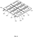
- Fig. 2 shows an embodiment of an electrically insulative substrate 250 of flat-plate-shaped.
- the electrically insulative substrate 250 has an upper flat surface which is separated into eight flat areas by four separation walls 2511, 2513, 2515, 2517 protruding from the upper flat surface.
- the flat area 2521 is separated by the separation walls 2511, 2517.
- the separation walls 2511, 2513, 2515, 2517 are formed integrally with the electrically insulative substrate 250.
- the separation walls 2511, 2513, 2515, 2517 not only can enhance creepage distance for isolation between two adjacent power semiconductor devices, but also can improve the mechanical strength of the electrically insulative substrate 250.
- the separation walls 2511, 2513, 2515, 2517 may be very thick, so that the upper flat surface of the electrically insulative substrate 250 is pocket-like.
- a flow channel 2530 is inside the electrically insulative substrate 250. As shown in Fig. 2 , the flow channel 2530 comprises an inlet 2531 and an outlet 2532 for allowing a coolant to flow in and flow out respectively. In some embodiments, the flow channel 2530 may have more than one inlet or outlet. The flow channel 2530 between the inlet 2531 and the outlet 2532 may be designed to make sure that the coolant can flow through every flat area of the electrically insulative substrate 250 where the power semiconductor device is fixed. In some embodiments, the flow channel 2530 may be one or more cavities inside the electrically insulative substrate 250. In addition, the flow channel 2530 may have various patterns, such as S-shaped, U-shaped, M-shaped.
- the flow channel 2530 comprises a serpentine pattern.
- the pattern of the flow channel 2530 is designed according to the heat dissipation requirement of each power semiconductor device placed on each of the flat areas. For example, for a power semiconductor device which may generate more heat than others, an increased heat exchange area of the flow channel 2530 under this power semiconductor device may be employed. And the power semiconductor device which may generate more heat may be disposed near the inlet 2531 of the flow channel 2530.
- the coolant flowing through the flow channel inside the electrically insulative substrate is a fluid which can remove the heat produced by the power semiconductor devices.
- An ideal coolant has high thermal capacity, low viscosity, is low cost, non-toxic, chemical inert, and neither causes nor promotes corrosion of the cooling channels.
- the most common coolant is water, preferably, deionized water. The very pure deionized water, due to its relatively low electrical conductivity, is very suitable to cool these electrical devices.
- each of the flat areas of the electrically insulative substrate 250 may further comprise a hole, for example, the flat area 2521 comprises a hole 2541.
- the hole 2541 is covered and can eliminate an electrically insulative layer between the coolant in the flow channel 2530 and the power semiconductor device, to realize direct contact and increase heat transfer.
- the size and shape of the hole 2541 may vary as long as the hole 2541 can be covered by the power semiconductor device disposed on the flat area 2521, and there is no coolant leakage from the hole 2541.
- the holes in the eight flat areas are all rectangular-shaped.
- the electrically insulative substrate 250 is made from one or more electrically insulative materials.
- the electrically insulative material may be a plastic material, a ceramic matrix composite material, a polymer matrix composite material, or any suitable advanced material entering the market.
- the electrically insulative substrate 250 is made from a thermoplastic material, such as ployphenylene sulfide (PPS), polyamide (PA), polytetrafluoroethylene (PTFE) or a combination thereof.
- PPS ployphenylene sulfide
- PA polyamide
- PTFE polytetrafluoroethylene
- the heat sinks where the power semiconductor devices are fixed are usually made of aluminum.
- the present disclosure employs an electrically insulative material, which may greatly enhance creepage distance for isolation and realize more tight packaging structure.
- the other advantage of employing an electrically insulative material maybe light weight. So light weight electronic equipment, such as power converter, may be achieved with the integrated packaging apparatus of the present disclosure.
- the electrically insulative substrate 250 is formed integrally.
- one or more thermoplastic materials are used as raw materials, and the manufacturing process may include various polymer processing techniques such as injection molding, compression molding, calendering, and extrusion.
- injection molding is used to produce the electrically insulative substrate 250.
- additive manufacturing or 3D printing technology may also be used for manufacturing of the electrically insulative substrate 250. Additive manufacturing, which builds 3D objects by adding layer-upon-layer of material, can produce complex, precisely designed shapes. Therefore, for the manufacturing of the electrically insulative substrate 250 with a flow channel inside, additive manufacturing is a good choice to be employed, in particular for an electrically insulative substrate with a special designed flow channel inside. Since the electrically insulative substrate 250 is formed integrally, the packaging apparatus has fewer components, so the automatic assembly and manufacturing of the integrated packaging apparatus become easier.
- Fig. 3 shows an integrated power semiconductor packaging apparatus 200 with the electrically insulative substrate 250 of Fig. 2 .
- Each of eight power semiconductor devices 231 ⁇ 238 is respectively installed on one of the eight flat areas of the electrically insulative substrate 250 via a metal plate.
- the power semiconductor device 231 Take the power semiconductor device 231 as an example, the power semiconductor device 231 is fixed on a metal plate 241.
- the power semiconductor device 231 is installed on the flat area 2521 through coupling the metal plate 241 to the flat area 2521, so that the hole 2541 on the flat area 2521 ( Fig. 2 ) is covered by the metal plate 241.
- a coolant is flowing through the flow channel 2530, direct contact between the coolant and the metal plate 241 can be realized to improve cooling performance.
- the size of the hole 2541 is as large as possible to get a large heat exchange area.
- a fastener such as screw
- a sealing ring such as a rubber sealing ring
- the other power semiconductor devices 232-238 may be installed on their corresponding flat areas with a similar method to the power semiconductor device 231.
- At least one of the power semiconductor devices 231 ⁇ 238 of the integrated packaging apparatus 200 may comprise an insulated-gate bipolar transistor (IGBT), a metal-oxide-semiconductor field-effect transistor (MOSFET), or a diode.
- IGBT insulated-gate bipolar transistor
- MOSFET metal-oxide-semiconductor field-effect transistor
- diode a diode.
- at least one of the power semiconductor devices 231-238 comprises a silicon carbide (SiC) power semiconductor device or a gallium nitride (GaN) power semiconductor device.
- the integrated power semiconductor packaging apparatus 200 of the present disclosure may minimize the packaging size of multiple power semiconductor devices and improve the power density. With the integrated packaging apparatus 200 of the present disclosure, low cost, light weight and high power density electronic equipment, such as power converter, may be achieved.
- the present disclosure also relates to a power converter including the integrated power semiconductor packaging apparatus as described above. It should be understood that besides the integrated power semiconductor packaging apparatus, the power converter may also comprise other appropriate components and/or circuits to achieve a required function of the power converter.
Landscapes
- Cooling Or The Like Of Semiconductors Or Solid State Devices (AREA)
- Inverter Devices (AREA)
Abstract
Description
- The present disclosure generally relates to an integrated power semiconductor packaging apparatus and a power converter containing the integrated power semiconductor packaging apparatus.
- Power electronic technologies could not do without power converters. Power converter is generic term of power electronic circuits and devices that used for power conversion. There are four basic power conversion models: DC/AC inversion, AC/AC frequency conversion, AC/DC rectification, and DC/DC conversion. Power converter may have various forms. Generally it includes basic elements of power semiconductor devices, circuits with various topologies, and different control strategies, which are called as "three elements of a power converter". Wherein the power semiconductor devices are basic elements, which are critical for the reliability, cost and performance of a power converter.
- Power semiconductor devices are electronic devices used as switches or rectifiers of a power converter. Due to the nature of the power semiconductor devices, the production of high power inevitably results in device power dissipation, which may damage the device and/or impair its performance. Therefore, packaging and cooling technology solutions are employed for the removal or dissipation of heat generated by the power semiconductor devices. Packaging is critical for the power density and assembly or manufacturing cost of an electronic equipment including multiple power semiconductor devices. The electronic equipment includes industrial low voltage, medium voltage drivers and converters, power inverters, etc.
- A conventional packaging structure for power semiconductor devices usually comprises a mounting plate and multiple heat sinks. Every power semiconductor device is fixed on an upper surface of a heat sink through a metal plate at the bottom of the power semiconductor device. A thermal grease is applied on a contact surface of the metal plate and the heat sink to realize close contact, avoid air gaps and improve heat transfer. Each heat sink has a flow channel inside it for a coolant flowing through to remove heat generated by the power semiconductor devices. The multiple heat sinks are installed on the common mounting plate to form a whole unit. A configuration of a conventional packaging structure is shown in
Fig. 1 . There are fourheat sinks mounting plate 110. Taking theheat sink 121 as an example, theheat sink 121 comprises a flat surface which is separated into twoflat areas separation wall 1212 protruding from the flat surface. Apower semiconductor devices 131 has a bottom fixed on ametal plate 141. Themetal plate 141 is installed on theheat sink 121, so that thepower semiconductor device 131 is fixed on theflat area 1213 of theheat sink 121. A thermal grease is placed between themetal plate 141 and theflat area 1213. The otherpower semiconductor device 132 is installed on theflat area 1214 of theheat sink 121 with the same method. Theheat sink 121 comprises a flow channel (not shown inFig. 1 ) inside it which has aninlet 1215 and anoutlet 1216 for allowing a coolant to flow in and flow out respectively. The coolant, such as water, air, or other fluid is forced to flow through the flow channel, so that the heat transferred from thepower semiconductor devices heat sinks 121 can be removed by the coolant. Each of the other heat sinks 122, 123, 124 has a similar structure to theheat sink 121. As mentioned above, the conventional packaging structure usually comprises many components including the mounting plate, the multiple heat sinks, multiple metal plates, and the thermal grease. Thus, the conventional packaging structure usually has a complex structure, and results in high manufacture and assembly cost. - Therefore, there is a need for improved power semiconductor packaging apparatus to solve at least one of the above-mentioned issues.
- One aspect of the present disclosure provides an integrated power semiconductor packaging apparatus. The integrated power semiconductor packaging apparatus comprises a plurality of power semiconductor devices and an electrically insulative substrate formed integrally. The electrically insulative substrate comprises a flat surface, at least one separation wall protruding from the flat surface and a flow channel inside the electrically insulative substrate. The at least one separation wall is configured to separate the flat surface into a plurality of flat areas. Each of the flat areas is configured to receive one of the power semiconductor devices. The flow channel is configured for allowing a coolant flowing through to remove heat generated from the plurality of power semiconductor devices.
- Another aspect of the present disclosure provides a power converter. The power converter comprises an integrated power semiconductor packaging apparatus which comprises a plurality of power semiconductor devices and an electrically insulative substrate formed integrally. The electrically insulative substrate comprises a flat surface, at least one separation wall protruding from the flat surface and a flow channel inside the electrically insulative substrate. The at least one separation wall is configured to separate the flat surface into a plurality of flat areas. Each of the flat areas is configured to receive one of the power semiconductor devices. The flow channel is configured for allowing a coolant flowing through to remove heat from the plurality of power semiconductor devices.
- The present disclosure provides an integrated packaging apparatus with a cooling flow channel, which can provide electrical insulation and mechanical support for multiple power semiconductor devices. It eliminates the use of thermal grease. In addition, since an electrically insulative material is used as a substrate for the power semiconductor devices, the creepage distance for isolation is enhanced and more tight packaging can be realized.
- The above and other aspects, features, and advantages of the present disclosure will become more apparent in light of the subsequent detailed description when taken in conjunction with the accompanying drawings in which:
-
Fig. 1 is a schematic diagram of a conventional power semiconductor packaging apparatus; -
Fig. 2 is a schematic diagram of an electrically insulative substrate in accordance with one embodiment of the present disclosure; and -
Fig. 3 a schematic diagram of an integrated power semiconductor packaging apparatus in accordance with one embodiment of the present disclosure. - Unless defined otherwise, technical and scientific terms used herein have the same meaning as is commonly understood by one of skill in the art to which this invention belongs. The terms "a" and "an" do not denote a limitation of quantity, but rather denote the presence of at least one of the referenced items. Approximating language, as used herein throughout the specification and claims, may be applied to modify any quantitative representation that could permissibly vary without resulting in a change in the basic function to which it is related. Accordingly, a value modified by a term or terms, such as "about" and "substantially", are not to be limited to the precise value specified. Additionally, when using an expression of "about a first value - a second value," the about is intended to modify both values. In at least some instances, the approximating language may correspond to the precision of an instrument for measuring the value. Here, and throughout the specification and claims, range limitations may be combined and/or interchanged, such ranges are identified and include all the sub-ranges contained therein unless context or language indicates otherwise. Moreover, the suffix "(s)" as used herein is usually intended to include both the singular and the plural of the term that it modifies, thereby including one or more of that term.
- Any numerical values recited herein include all values from the lower value to the upper value in increments of one unit provided that there is a separation of at least 2 units between any lower value and any higher value. As an example, if it is stated that the amount of a component or a value of a process variable such as, for example, temperature, pressure, time and the like is, for example, from 1 to 90, it is intended that values such as 15 to 85, 22 to 68, 43 to 51, 30 to 32 etc. are expressly enumerated in this specification. For values which are less than one, one unit is considered to be 0.0001, 0.001, 0.01 or 0.1 as appropriate. These are only examples of what is specifically intended and all possible combinations of numerical values between the lowest value and the highest value enumerated are to be considered to be expressly stated in this application in a similar manner.
- The present disclosure relates to an integrated power semiconductor packaging apparatus, comprising a plurality of power semiconductor devices and an electrically insulative substrate formed integrally. The electrically insulative substrate comprises a flat surface, at least one separation wall protruding from the flat surface and a flow channel inside the electrically insulative substrate. The at least one separation wall is configured to separate the flat surface into a plurality of flat areas. Each of the flat areas is configured to receive one of the power semiconductor devices. The flow channel is configured for allowing a coolant flowing through to remove heat from the plurality of power semiconductor devices.
- The plurality of power semiconductor devices may be all the same, or, at least two of the power semiconductor devices are different from each other. The number, type, size, and position arrangement of the power semiconductor devices on the electrically insulative substrate depend on the function requirements and specific needs of an electronic equipment adopting the integrated packaging apparatus of the present disclosure.
- The shape of the electrically insulative substrate may be various. Preferably, the electrically insulative substrate is flat-plate-shaped having an upper flat surface and a bottom flat surface opposite to the upper flat surface.
Fig. 2 shows an embodiment of anelectrically insulative substrate 250 of flat-plate-shaped. As shown inFig. 2 , the electricallyinsulative substrate 250 has an upper flat surface which is separated into eight flat areas by fourseparation walls flat area 2521 is separated by theseparation walls separation walls electrically insulative substrate 250. Theseparation walls electrically insulative substrate 250. In some embodiments, theseparation walls electrically insulative substrate 250 is pocket-like. - A
flow channel 2530 is inside the electricallyinsulative substrate 250. As shown inFig. 2 , theflow channel 2530 comprises aninlet 2531 and anoutlet 2532 for allowing a coolant to flow in and flow out respectively. In some embodiments, theflow channel 2530 may have more than one inlet or outlet. Theflow channel 2530 between theinlet 2531 and theoutlet 2532 may be designed to make sure that the coolant can flow through every flat area of theelectrically insulative substrate 250 where the power semiconductor device is fixed. In some embodiments, theflow channel 2530 may be one or more cavities inside the electricallyinsulative substrate 250. In addition, theflow channel 2530 may have various patterns, such as S-shaped, U-shaped, M-shaped. Preferably, theflow channel 2530 comprises a serpentine pattern. In some embodiments, the pattern of theflow channel 2530 is designed according to the heat dissipation requirement of each power semiconductor device placed on each of the flat areas. For example, for a power semiconductor device which may generate more heat than others, an increased heat exchange area of theflow channel 2530 under this power semiconductor device may be employed. And the power semiconductor device which may generate more heat may be disposed near theinlet 2531 of theflow channel 2530. - The coolant flowing through the flow channel inside the electrically insulative substrate is a fluid which can remove the heat produced by the power semiconductor devices. An ideal coolant has high thermal capacity, low viscosity, is low cost, non-toxic, chemical inert, and neither causes nor promotes corrosion of the cooling channels. The most common coolant is water, preferably, deionized water. The very pure deionized water, due to its relatively low electrical conductivity, is very suitable to cool these electrical devices.
- As shown in
Fig. 2 , each of the flat areas of theelectrically insulative substrate 250 may further comprise a hole, for example, theflat area 2521 comprises ahole 2541. When a power semiconductor device is disposed on theflat area 2521, thehole 2541 is covered and can eliminate an electrically insulative layer between the coolant in theflow channel 2530 and the power semiconductor device, to realize direct contact and increase heat transfer. The size and shape of thehole 2541 may vary as long as thehole 2541 can be covered by the power semiconductor device disposed on theflat area 2521, and there is no coolant leakage from thehole 2541. InFig. 2 , the holes in the eight flat areas are all rectangular-shaped. - Usually, the electrically
insulative substrate 250 is made from one or more electrically insulative materials. The electrically insulative material may be a plastic material, a ceramic matrix composite material, a polymer matrix composite material, or any suitable advanced material entering the market. In some embodiments, the electricallyinsulative substrate 250 is made from a thermoplastic material, such as ployphenylene sulfide (PPS), polyamide (PA), polytetrafluoroethylene (PTFE) or a combination thereof. In the conventional packaging structure described above, the heat sinks where the power semiconductor devices are fixed are usually made of aluminum. The present disclosure employs an electrically insulative material, which may greatly enhance creepage distance for isolation and realize more tight packaging structure. The other advantage of employing an electrically insulative material maybe light weight. So light weight electronic equipment, such as power converter, may be achieved with the integrated packaging apparatus of the present disclosure. - The
electrically insulative substrate 250 is formed integrally. In some embodiments, one or more thermoplastic materials are used as raw materials, and the manufacturing process may include various polymer processing techniques such as injection molding, compression molding, calendering, and extrusion. Preferably, injection molding is used to produce theelectrically insulative substrate 250. In addition, additive manufacturing or 3D printing technology may also be used for manufacturing of theelectrically insulative substrate 250. Additive manufacturing, which builds 3D objects by adding layer-upon-layer of material, can produce complex, precisely designed shapes. Therefore, for the manufacturing of theelectrically insulative substrate 250 with a flow channel inside, additive manufacturing is a good choice to be employed, in particular for an electrically insulative substrate with a special designed flow channel inside. Since the electricallyinsulative substrate 250 is formed integrally, the packaging apparatus has fewer components, so the automatic assembly and manufacturing of the integrated packaging apparatus become easier. -
Fig. 3 shows an integrated powersemiconductor packaging apparatus 200 with theelectrically insulative substrate 250 ofFig. 2 . Each of eightpower semiconductor devices 231∼238 is respectively installed on one of the eight flat areas of theelectrically insulative substrate 250 via a metal plate. Take thepower semiconductor device 231 as an example, thepower semiconductor device 231 is fixed on ametal plate 241. Thepower semiconductor device 231 is installed on theflat area 2521 through coupling themetal plate 241 to theflat area 2521, so that thehole 2541 on the flat area 2521 (Fig. 2 ) is covered by themetal plate 241. When a coolant is flowing through theflow channel 2530, direct contact between the coolant and themetal plate 241 can be realized to improve cooling performance. Usually, the size of thehole 2541 is as large as possible to get a large heat exchange area. In addition, it is critical to seal themetal plate 241 and thehole 2541 to prevent leakage of the coolant. One example is to use a fastener, such as screw, and a sealing ring, such as a rubber sealing ring, to fix themetal plate 241 to theflat area 2521 and cover thehole 2541. The other power semiconductor devices 232-238 may be installed on their corresponding flat areas with a similar method to thepower semiconductor device 231. - At least one of the
power semiconductor devices 231∼238 of theintegrated packaging apparatus 200 may comprise an insulated-gate bipolar transistor (IGBT), a metal-oxide-semiconductor field-effect transistor (MOSFET), or a diode. In some embodiments, at least one of the power semiconductor devices 231-238 comprises a silicon carbide (SiC) power semiconductor device or a gallium nitride (GaN) power semiconductor device. - The integrated power
semiconductor packaging apparatus 200 of the present disclosure may minimize the packaging size of multiple power semiconductor devices and improve the power density. With the integratedpackaging apparatus 200 of the present disclosure, low cost, light weight and high power density electronic equipment, such as power converter, may be achieved. - The present disclosure also relates to a power converter including the integrated power semiconductor packaging apparatus as described above. It should be understood that besides the integrated power semiconductor packaging apparatus, the power converter may also comprise other appropriate components and/or circuits to achieve a required function of the power converter.
- This written description uses examples to describe the disclosure, including the best mode, and also to enable any person skilled in the art to practice the disclosure, including making and using any devices or systems and performing any incorporated methods. The patentable scope of the disclosure is defined by the claims, and may include other examples that occur to those skilled in the art. Such other examples are intended to be within the scope of the claims if they have structural elements that do not differ from the literal language of the claims, or if they include equivalent structural elements with insubstantial differences from the literal languages of the claims.
Claims (10)
- An integrated power semiconductor packaging apparatus (200), comprising:a plurality of power semiconductor devices (231-238); andan electrically insulative substrate (250) formed integrally, comprising:a flat surface (2521);at least one separation wall (2511,2513,2515,2517) protruding from the flat surface and configured to separate the flat surface into a plurality of flat areas (2521), wherein each of the flat areas (2521) is configured to receive one of the power semiconductor devices; anda flow channel (2530) inside the electrically insulative substrate (250) for allowing a coolant flowing through to remove heat from the plurality of power semiconductor devices (231-238).
- The apparatus of claim 1, wherein one power semiconductor device (231-238) is fixed on a metal plate (241), the metal plate (241) is installed on one of the flat areas (2521), and the one flat area comprises a hole (2541) to realize direct contact between the coolant in the flow channel (2530) and the metal plate (241).
- The apparatus of claim 2, wherein the metal plate (241) is installed on the one flat area (2521) through a fastener and a sealing ring.
- The apparatus of any of claims 1 to 3, wherein the electrically insulative substrate (250) comprises a plastic material, a ceramic matrix composite material or a polymer matrix composite material.
- The apparatus of any of claims 1 to 4, wherein the electrically insulative substrate (250) is formed by injection molding or additive manufacturing process.
- The apparatus of any preceding claim, wherein the coolant comprises deionized water.
- The apparatus of any preceding claim, wherein the flow channel (2530) is a serpentine channel.
- The apparatus of any preceding claim, wherein one of the power semiconductor devices (231-238) comprises an insulated-gate bipolar transistor, a metal-oxide-semiconductor field-effect transistor, or a diode.
- The apparatus of any of claims 1 to 7, wherein one of the power semiconductor devices comprises a silicon carbide power semiconductor device or a gallium nitride power semiconductor device.
- A power converter, comprising an integrated power semiconductor packaging apparatus, the integrated power semiconductor packaging apparatus as defined in any preceding claim.
Applications Claiming Priority (1)
| Application Number | Priority Date | Filing Date | Title |
|---|---|---|---|
| CN201710347397.5A CN108962853A (en) | 2017-05-17 | 2017-05-17 | Integrated power semiconductor packaging apparatus and power inverter |
Publications (2)
| Publication Number | Publication Date |
|---|---|
| EP3404711A1 true EP3404711A1 (en) | 2018-11-21 |
| EP3404711B1 EP3404711B1 (en) | 2021-10-20 |
Family
ID=62091686
Family Applications (1)
| Application Number | Title | Priority Date | Filing Date |
|---|---|---|---|
| EP18169391.2A Not-in-force EP3404711B1 (en) | 2017-05-17 | 2018-04-26 | Integrated power semiconductor packaging apparatus and power converter |
Country Status (4)
| Country | Link |
|---|---|
| US (1) | US10497642B2 (en) |
| EP (1) | EP3404711B1 (en) |
| CN (1) | CN108962853A (en) |
| ES (1) | ES2906108T3 (en) |
Cited By (1)
| Publication number | Priority date | Publication date | Assignee | Title |
|---|---|---|---|---|
| EP3996133A4 (en) * | 2019-07-02 | 2022-07-13 | Mitsubishi Electric Corporation | POWER MODULE AND METHOD OF MANUFACTURING IT |
Families Citing this family (3)
| Publication number | Priority date | Publication date | Assignee | Title |
|---|---|---|---|---|
| US11699634B2 (en) | 2019-05-03 | 2023-07-11 | Applied Materials, Inc. | Water cooled plate for heat management in power amplifiers |
| CN113437037B (en) * | 2021-06-29 | 2024-05-24 | 中创杜菲(北京)汽车科技有限公司 | Power semiconductor package cooling device |
| US12176687B2 (en) | 2022-05-23 | 2024-12-24 | Hamilton Sundstrand Corporation | Power converter |
Citations (2)
| Publication number | Priority date | Publication date | Assignee | Title |
|---|---|---|---|---|
| JPS5595352A (en) * | 1979-01-12 | 1980-07-19 | Nippon Telegr & Teleph Corp <Ntt> | Integrated circuit structure |
| US20100175857A1 (en) * | 2009-01-15 | 2010-07-15 | General Electric Company | Millichannel heat sink, and stack and apparatus using the same |
Family Cites Families (15)
| Publication number | Priority date | Publication date | Assignee | Title |
|---|---|---|---|---|
| TW200503608A (en) * | 2003-07-15 | 2005-01-16 | Ind Tech Res Inst | Cooling plate having vortices generator |
| DE102004032605B4 (en) | 2004-07-05 | 2007-12-20 | Infineon Technologies Ag | Semiconductor component with a semiconductor chip and electrical connection elements to a conductor structure |
| JP2007251076A (en) * | 2006-03-20 | 2007-09-27 | Hitachi Ltd | Power semiconductor module |
| US7755186B2 (en) * | 2007-12-31 | 2010-07-13 | Intel Corporation | Cooling solutions for die-down integrated circuit packages |
| US7911792B2 (en) | 2008-03-11 | 2011-03-22 | Ford Global Technologies Llc | Direct dipping cooled power module and packaging |
| JP5457435B2 (en) | 2008-05-16 | 2014-04-02 | パーカー−ハニフイン・コーポレーシヨン | Modular high power drive stack cooled by vaporizable dielectric fluid |
| US8248809B2 (en) | 2008-08-26 | 2012-08-21 | GM Global Technology Operations LLC | Inverter power module with distributed support for direct substrate cooling |
| CN102060116B (en) | 2010-11-23 | 2015-04-22 | 上海骏图电子科技有限公司 | Post-packaging test equipment for plastic package surface mounted devices diode |
| US9111937B2 (en) | 2013-05-28 | 2015-08-18 | Freescale Semiconductor, Inc. | Semiconductor devices with multilayer flex interconnect structures |
| US20160211193A1 (en) * | 2013-08-30 | 2016-07-21 | Denso Corporation | Stacked cooler |
| JP6219342B2 (en) * | 2015-07-10 | 2017-10-25 | 株式会社日本製鋼所 | Inverter cooling method and inverter cooling apparatus for electric injection molding machine |
| WO2017093281A1 (en) * | 2015-11-30 | 2017-06-08 | At&S Austria Technologie & Systemtechnik Aktiengesellschaft | Electronic component packaged in component carrier serving as shielding cage |
| CN105632947A (en) | 2015-12-24 | 2016-06-01 | 合肥祖安投资合伙企业(有限合伙) | Semiconductor device packaging structure and manufacturing method thereof |
| US9953897B2 (en) * | 2016-07-22 | 2018-04-24 | Hewlett Packard Enterprise Development Lp | Fluid-filled microchannels |
| US10361143B2 (en) * | 2017-06-01 | 2019-07-23 | Raytheon Company | Apparatus and method for reconfigurable thermal management using flow control of liquid metal |
-
2017
- 2017-05-17 CN CN201710347397.5A patent/CN108962853A/en active Pending
-
2018
- 2018-04-26 EP EP18169391.2A patent/EP3404711B1/en not_active Not-in-force
- 2018-04-26 ES ES18169391T patent/ES2906108T3/en active Active
- 2018-05-17 US US15/981,975 patent/US10497642B2/en not_active Expired - Fee Related
Patent Citations (2)
| Publication number | Priority date | Publication date | Assignee | Title |
|---|---|---|---|---|
| JPS5595352A (en) * | 1979-01-12 | 1980-07-19 | Nippon Telegr & Teleph Corp <Ntt> | Integrated circuit structure |
| US20100175857A1 (en) * | 2009-01-15 | 2010-07-15 | General Electric Company | Millichannel heat sink, and stack and apparatus using the same |
Cited By (2)
| Publication number | Priority date | Publication date | Assignee | Title |
|---|---|---|---|---|
| EP3996133A4 (en) * | 2019-07-02 | 2022-07-13 | Mitsubishi Electric Corporation | POWER MODULE AND METHOD OF MANUFACTURING IT |
| US12014974B2 (en) | 2019-07-02 | 2024-06-18 | Mitsubishi Electric Corporation | Power module with electrodes and heat sink and manufacturing method therefor |
Also Published As
| Publication number | Publication date |
|---|---|
| CN108962853A (en) | 2018-12-07 |
| US20180337109A1 (en) | 2018-11-22 |
| EP3404711B1 (en) | 2021-10-20 |
| US10497642B2 (en) | 2019-12-03 |
| ES2906108T3 (en) | 2022-04-13 |
Similar Documents
| Publication | Publication Date | Title |
|---|---|---|
| US10497642B2 (en) | Integrated power semiconductor packaging apparatus and power converter | |
| CN105874592B (en) | Cooler and how to fix it | |
| US9331001B2 (en) | Semiconductor module | |
| EP2613350A1 (en) | Semiconductor module | |
| US20210274690A1 (en) | Power module and manufacturing method therefor, and inverter apparatus having power module | |
| US10199238B2 (en) | Semiconductor module cooling system | |
| CN106899215A (en) | Power inverter | |
| EP2423958A2 (en) | Integral heat sink with spiral manifolds | |
| CN102130070A (en) | Power electronics substrate for direct substrate cooling | |
| US11967899B2 (en) | Fluid cooled inverter | |
| CN107104086A (en) | Liquid-cooling heat radiator and electric machine controller | |
| US20160190032A1 (en) | Wiring board and semiconductor package including wiring board | |
| EP3460840B1 (en) | Devices for attaching and sealing a semiconductor cooling structure | |
| JP6286541B2 (en) | Power module device and power conversion device | |
| Zaman et al. | Compact 3D-printed jet-impingement nozzle for top-side-cooled GaN power devices | |
| CN206992093U (en) | Liquid-cooling heat radiator and electric machine controller | |
| CN117641833A (en) | Intermediate circuit assembly | |
| JP2015065310A (en) | Seal member, cooler and semiconductor device | |
| CN209104144U (en) | Cooled electrical equipment component | |
| RU2516227C2 (en) | Heat sink and unit for flat bodies, providing for cooling and assembly | |
| Skuriat | Direct jet impingement cooling of power electronics | |
| FI127831B (en) | Method of manufacturing a semiconductor module | |
| WO2023004661A1 (en) | Semiconductor arrangement | |
| CN121219838A (en) | Semiconductor power modules, semiconductor power packages, and methods for manufacturing semiconductor power modules | |
| WO2023228417A1 (en) | Heat dissipation structure for semiconductor device |
Legal Events
| Date | Code | Title | Description |
|---|---|---|---|
| PUAI | Public reference made under article 153(3) epc to a published international application that has entered the european phase |
Free format text: ORIGINAL CODE: 0009012 |
|
| STAA | Information on the status of an ep patent application or granted ep patent |
Free format text: STATUS: THE APPLICATION HAS BEEN PUBLISHED |
|
| AK | Designated contracting states |
Kind code of ref document: A1 Designated state(s): AL AT BE BG CH CY CZ DE DK EE ES FI FR GB GR HR HU IE IS IT LI LT LU LV MC MK MT NL NO PL PT RO RS SE SI SK SM TR |
|
| AX | Request for extension of the european patent |
Extension state: BA ME |
|
| STAA | Information on the status of an ep patent application or granted ep patent |
Free format text: STATUS: REQUEST FOR EXAMINATION WAS MADE |
|
| 17P | Request for examination filed |
Effective date: 20190514 |
|
| RBV | Designated contracting states (corrected) |
Designated state(s): AL AT BE BG CH CY CZ DE DK EE ES FI FR GB GR HR HU IE IS IT LI LT LU LV MC MK MT NL NO PL PT RO RS SE SI SK SM TR |
|
| STAA | Information on the status of an ep patent application or granted ep patent |
Free format text: STATUS: EXAMINATION IS IN PROGRESS |
|
| 17Q | First examination report despatched |
Effective date: 20191111 |
|
| GRAP | Despatch of communication of intention to grant a patent |
Free format text: ORIGINAL CODE: EPIDOSNIGR1 |
|
| STAA | Information on the status of an ep patent application or granted ep patent |
Free format text: STATUS: GRANT OF PATENT IS INTENDED |
|
| INTG | Intention to grant announced |
Effective date: 20210521 |
|
| GRAS | Grant fee paid |
Free format text: ORIGINAL CODE: EPIDOSNIGR3 |
|
| GRAA | (expected) grant |
Free format text: ORIGINAL CODE: 0009210 |
|
| STAA | Information on the status of an ep patent application or granted ep patent |
Free format text: STATUS: THE PATENT HAS BEEN GRANTED |
|
| AK | Designated contracting states |
Kind code of ref document: B1 Designated state(s): AL AT BE BG CH CY CZ DE DK EE ES FI FR GB GR HR HU IE IS IT LI LT LU LV MC MK MT NL NO PL PT RO RS SE SI SK SM TR |
|
| REG | Reference to a national code |
Ref country code: GB Ref legal event code: FG4D |
|
| REG | Reference to a national code |
Ref country code: CH Ref legal event code: EP |
|
| REG | Reference to a national code |
Ref country code: IE Ref legal event code: FG4D |
|
| REG | Reference to a national code |
Ref country code: DE Ref legal event code: R096 Ref document number: 602018025189 Country of ref document: DE |
|
| REG | Reference to a national code |
Ref country code: AT Ref legal event code: REF Ref document number: 1440625 Country of ref document: AT Kind code of ref document: T Effective date: 20211115 |
|
| REG | Reference to a national code |
Ref country code: LT Ref legal event code: MG9D |
|
| REG | Reference to a national code |
Ref country code: NL Ref legal event code: MP Effective date: 20211020 |
|
| REG | Reference to a national code |
Ref country code: AT Ref legal event code: MK05 Ref document number: 1440625 Country of ref document: AT Kind code of ref document: T Effective date: 20211020 |
|
| REG | Reference to a national code |
Ref country code: ES Ref legal event code: FG2A Ref document number: 2906108 Country of ref document: ES Kind code of ref document: T3 Effective date: 20220413 |
|
| PG25 | Lapsed in a contracting state [announced via postgrant information from national office to epo] |
Ref country code: RS Free format text: LAPSE BECAUSE OF FAILURE TO SUBMIT A TRANSLATION OF THE DESCRIPTION OR TO PAY THE FEE WITHIN THE PRESCRIBED TIME-LIMIT Effective date: 20211020 Ref country code: LT Free format text: LAPSE BECAUSE OF FAILURE TO SUBMIT A TRANSLATION OF THE DESCRIPTION OR TO PAY THE FEE WITHIN THE PRESCRIBED TIME-LIMIT Effective date: 20211020 Ref country code: FI Free format text: LAPSE BECAUSE OF FAILURE TO SUBMIT A TRANSLATION OF THE DESCRIPTION OR TO PAY THE FEE WITHIN THE PRESCRIBED TIME-LIMIT Effective date: 20211020 Ref country code: BG Free format text: LAPSE BECAUSE OF FAILURE TO SUBMIT A TRANSLATION OF THE DESCRIPTION OR TO PAY THE FEE WITHIN THE PRESCRIBED TIME-LIMIT Effective date: 20220120 Ref country code: AT Free format text: LAPSE BECAUSE OF FAILURE TO SUBMIT A TRANSLATION OF THE DESCRIPTION OR TO PAY THE FEE WITHIN THE PRESCRIBED TIME-LIMIT Effective date: 20211020 |
|
| PGFP | Annual fee paid to national office [announced via postgrant information from national office to epo] |
Ref country code: IE Payment date: 20220323 Year of fee payment: 5 Ref country code: GB Payment date: 20220323 Year of fee payment: 5 |
|
| PG25 | Lapsed in a contracting state [announced via postgrant information from national office to epo] |
Ref country code: IS Free format text: LAPSE BECAUSE OF FAILURE TO SUBMIT A TRANSLATION OF THE DESCRIPTION OR TO PAY THE FEE WITHIN THE PRESCRIBED TIME-LIMIT Effective date: 20220220 Ref country code: SE Free format text: LAPSE BECAUSE OF FAILURE TO SUBMIT A TRANSLATION OF THE DESCRIPTION OR TO PAY THE FEE WITHIN THE PRESCRIBED TIME-LIMIT Effective date: 20211020 Ref country code: PT Free format text: LAPSE BECAUSE OF FAILURE TO SUBMIT A TRANSLATION OF THE DESCRIPTION OR TO PAY THE FEE WITHIN THE PRESCRIBED TIME-LIMIT Effective date: 20220221 Ref country code: PL Free format text: LAPSE BECAUSE OF FAILURE TO SUBMIT A TRANSLATION OF THE DESCRIPTION OR TO PAY THE FEE WITHIN THE PRESCRIBED TIME-LIMIT Effective date: 20211020 Ref country code: NO Free format text: LAPSE BECAUSE OF FAILURE TO SUBMIT A TRANSLATION OF THE DESCRIPTION OR TO PAY THE FEE WITHIN THE PRESCRIBED TIME-LIMIT Effective date: 20220120 Ref country code: NL Free format text: LAPSE BECAUSE OF FAILURE TO SUBMIT A TRANSLATION OF THE DESCRIPTION OR TO PAY THE FEE WITHIN THE PRESCRIBED TIME-LIMIT Effective date: 20211020 Ref country code: LV Free format text: LAPSE BECAUSE OF FAILURE TO SUBMIT A TRANSLATION OF THE DESCRIPTION OR TO PAY THE FEE WITHIN THE PRESCRIBED TIME-LIMIT Effective date: 20211020 Ref country code: HR Free format text: LAPSE BECAUSE OF FAILURE TO SUBMIT A TRANSLATION OF THE DESCRIPTION OR TO PAY THE FEE WITHIN THE PRESCRIBED TIME-LIMIT Effective date: 20211020 Ref country code: GR Free format text: LAPSE BECAUSE OF FAILURE TO SUBMIT A TRANSLATION OF THE DESCRIPTION OR TO PAY THE FEE WITHIN THE PRESCRIBED TIME-LIMIT Effective date: 20220121 |
|
| PGFP | Annual fee paid to national office [announced via postgrant information from national office to epo] |
Ref country code: FR Payment date: 20220322 Year of fee payment: 5 |
|
| REG | Reference to a national code |
Ref country code: DE Ref legal event code: R097 Ref document number: 602018025189 Country of ref document: DE |
|
| PG25 | Lapsed in a contracting state [announced via postgrant information from national office to epo] |
Ref country code: SM Free format text: LAPSE BECAUSE OF FAILURE TO SUBMIT A TRANSLATION OF THE DESCRIPTION OR TO PAY THE FEE WITHIN THE PRESCRIBED TIME-LIMIT Effective date: 20211020 Ref country code: SK Free format text: LAPSE BECAUSE OF FAILURE TO SUBMIT A TRANSLATION OF THE DESCRIPTION OR TO PAY THE FEE WITHIN THE PRESCRIBED TIME-LIMIT Effective date: 20211020 Ref country code: RO Free format text: LAPSE BECAUSE OF FAILURE TO SUBMIT A TRANSLATION OF THE DESCRIPTION OR TO PAY THE FEE WITHIN THE PRESCRIBED TIME-LIMIT Effective date: 20211020 Ref country code: EE Free format text: LAPSE BECAUSE OF FAILURE TO SUBMIT A TRANSLATION OF THE DESCRIPTION OR TO PAY THE FEE WITHIN THE PRESCRIBED TIME-LIMIT Effective date: 20211020 Ref country code: DK Free format text: LAPSE BECAUSE OF FAILURE TO SUBMIT A TRANSLATION OF THE DESCRIPTION OR TO PAY THE FEE WITHIN THE PRESCRIBED TIME-LIMIT Effective date: 20211020 Ref country code: CZ Free format text: LAPSE BECAUSE OF FAILURE TO SUBMIT A TRANSLATION OF THE DESCRIPTION OR TO PAY THE FEE WITHIN THE PRESCRIBED TIME-LIMIT Effective date: 20211020 |
|
| PGFP | Annual fee paid to national office [announced via postgrant information from national office to epo] |
Ref country code: ES Payment date: 20220502 Year of fee payment: 5 Ref country code: DE Payment date: 20220322 Year of fee payment: 5 |
|
| PLBE | No opposition filed within time limit |
Free format text: ORIGINAL CODE: 0009261 |
|
| STAA | Information on the status of an ep patent application or granted ep patent |
Free format text: STATUS: NO OPPOSITION FILED WITHIN TIME LIMIT |
|
| 26N | No opposition filed |
Effective date: 20220721 |
|
| PG25 | Lapsed in a contracting state [announced via postgrant information from national office to epo] |
Ref country code: AL Free format text: LAPSE BECAUSE OF FAILURE TO SUBMIT A TRANSLATION OF THE DESCRIPTION OR TO PAY THE FEE WITHIN THE PRESCRIBED TIME-LIMIT Effective date: 20211020 |
|
| PG25 | Lapsed in a contracting state [announced via postgrant information from national office to epo] |
Ref country code: SI Free format text: LAPSE BECAUSE OF FAILURE TO SUBMIT A TRANSLATION OF THE DESCRIPTION OR TO PAY THE FEE WITHIN THE PRESCRIBED TIME-LIMIT Effective date: 20211020 |
|
| REG | Reference to a national code |
Ref country code: CH Ref legal event code: PL |
|
| REG | Reference to a national code |
Ref country code: BE Ref legal event code: MM Effective date: 20220430 |
|
| PG25 | Lapsed in a contracting state [announced via postgrant information from national office to epo] |
Ref country code: MC Free format text: LAPSE BECAUSE OF FAILURE TO SUBMIT A TRANSLATION OF THE DESCRIPTION OR TO PAY THE FEE WITHIN THE PRESCRIBED TIME-LIMIT Effective date: 20211020 Ref country code: LU Free format text: LAPSE BECAUSE OF NON-PAYMENT OF DUE FEES Effective date: 20220426 Ref country code: LI Free format text: LAPSE BECAUSE OF NON-PAYMENT OF DUE FEES Effective date: 20220430 Ref country code: CH Free format text: LAPSE BECAUSE OF NON-PAYMENT OF DUE FEES Effective date: 20220430 |
|
| PG25 | Lapsed in a contracting state [announced via postgrant information from national office to epo] |
Ref country code: BE Free format text: LAPSE BECAUSE OF NON-PAYMENT OF DUE FEES Effective date: 20220430 |
|
| PG25 | Lapsed in a contracting state [announced via postgrant information from national office to epo] |
Ref country code: IT Free format text: LAPSE BECAUSE OF FAILURE TO SUBMIT A TRANSLATION OF THE DESCRIPTION OR TO PAY THE FEE WITHIN THE PRESCRIBED TIME-LIMIT Effective date: 20211020 |
|
| REG | Reference to a national code |
Ref country code: DE Ref legal event code: R119 Ref document number: 602018025189 Country of ref document: DE |
|
| GBPC | Gb: european patent ceased through non-payment of renewal fee |
Effective date: 20230426 |
|
| PG25 | Lapsed in a contracting state [announced via postgrant information from national office to epo] |
Ref country code: GB Free format text: LAPSE BECAUSE OF NON-PAYMENT OF DUE FEES Effective date: 20230426 |
|
| PG25 | Lapsed in a contracting state [announced via postgrant information from national office to epo] |
Ref country code: GB Free format text: LAPSE BECAUSE OF NON-PAYMENT OF DUE FEES Effective date: 20230426 Ref country code: FR Free format text: LAPSE BECAUSE OF NON-PAYMENT OF DUE FEES Effective date: 20230430 Ref country code: DE Free format text: LAPSE BECAUSE OF NON-PAYMENT OF DUE FEES Effective date: 20231103 |
|
| REG | Reference to a national code |
Ref country code: IE Ref legal event code: MM4A |
|
| PG25 | Lapsed in a contracting state [announced via postgrant information from national office to epo] |
Ref country code: HU Free format text: LAPSE BECAUSE OF FAILURE TO SUBMIT A TRANSLATION OF THE DESCRIPTION OR TO PAY THE FEE WITHIN THE PRESCRIBED TIME-LIMIT; INVALID AB INITIO Effective date: 20180426 |
|
| PG25 | Lapsed in a contracting state [announced via postgrant information from national office to epo] |
Ref country code: IE Free format text: LAPSE BECAUSE OF NON-PAYMENT OF DUE FEES Effective date: 20230426 |
|
| PG25 | Lapsed in a contracting state [announced via postgrant information from national office to epo] |
Ref country code: MK Free format text: LAPSE BECAUSE OF FAILURE TO SUBMIT A TRANSLATION OF THE DESCRIPTION OR TO PAY THE FEE WITHIN THE PRESCRIBED TIME-LIMIT Effective date: 20211020 Ref country code: IE Free format text: LAPSE BECAUSE OF NON-PAYMENT OF DUE FEES Effective date: 20230426 Ref country code: CY Free format text: LAPSE BECAUSE OF FAILURE TO SUBMIT A TRANSLATION OF THE DESCRIPTION OR TO PAY THE FEE WITHIN THE PRESCRIBED TIME-LIMIT Effective date: 20211020 |
|
| REG | Reference to a national code |
Ref country code: ES Ref legal event code: FD2A Effective date: 20240530 |
|
| PG25 | Lapsed in a contracting state [announced via postgrant information from national office to epo] |
Ref country code: TR Free format text: LAPSE BECAUSE OF FAILURE TO SUBMIT A TRANSLATION OF THE DESCRIPTION OR TO PAY THE FEE WITHIN THE PRESCRIBED TIME-LIMIT Effective date: 20211020 |
|
| PG25 | Lapsed in a contracting state [announced via postgrant information from national office to epo] |
Ref country code: ES Free format text: LAPSE BECAUSE OF NON-PAYMENT OF DUE FEES Effective date: 20230427 |
|
| PG25 | Lapsed in a contracting state [announced via postgrant information from national office to epo] |
Ref country code: ES Free format text: LAPSE BECAUSE OF NON-PAYMENT OF DUE FEES Effective date: 20230427 |
|
| PG25 | Lapsed in a contracting state [announced via postgrant information from national office to epo] |
Ref country code: MT Free format text: LAPSE BECAUSE OF FAILURE TO SUBMIT A TRANSLATION OF THE DESCRIPTION OR TO PAY THE FEE WITHIN THE PRESCRIBED TIME-LIMIT Effective date: 20211020 |