EP3402069A2 - Mehrstufige verstärkerschaltung mit null- und pol-einsatz durch kompensationsschaltungen - Google Patents
Mehrstufige verstärkerschaltung mit null- und pol-einsatz durch kompensationsschaltungen Download PDFInfo
- Publication number
- EP3402069A2 EP3402069A2 EP18162836.3A EP18162836A EP3402069A2 EP 3402069 A2 EP3402069 A2 EP 3402069A2 EP 18162836 A EP18162836 A EP 18162836A EP 3402069 A2 EP3402069 A2 EP 3402069A2
- Authority
- EP
- European Patent Office
- Prior art keywords
- amplifier
- circuit
- output port
- coupled
- compensation
- Prior art date
- Legal status (The legal status is an assumption and is not a legal conclusion. Google has not performed a legal analysis and makes no representation as to the accuracy of the status listed.)
- Granted
Links
Images




Classifications
-
- H—ELECTRICITY
- H03—ELECTRONIC CIRCUITRY
- H03F—AMPLIFIERS
- H03F1/00—Details of amplifiers with only discharge tubes, only semiconductor devices or only unspecified devices as amplifying elements
- H03F1/42—Modifications of amplifiers to extend the bandwidth
-
- H—ELECTRICITY
- H03—ELECTRONIC CIRCUITRY
- H03F—AMPLIFIERS
- H03F1/00—Details of amplifiers with only discharge tubes, only semiconductor devices or only unspecified devices as amplifying elements
- H03F1/08—Modifications of amplifiers to reduce detrimental influences of internal impedances of amplifying elements
- H03F1/083—Modifications of amplifiers to reduce detrimental influences of internal impedances of amplifying elements in transistor amplifiers
-
- H—ELECTRICITY
- H03—ELECTRONIC CIRCUITRY
- H03F—AMPLIFIERS
- H03F1/00—Details of amplifiers with only discharge tubes, only semiconductor devices or only unspecified devices as amplifying elements
- H03F1/08—Modifications of amplifiers to reduce detrimental influences of internal impedances of amplifying elements
- H03F1/083—Modifications of amplifiers to reduce detrimental influences of internal impedances of amplifying elements in transistor amplifiers
- H03F1/086—Modifications of amplifiers to reduce detrimental influences of internal impedances of amplifying elements in transistor amplifiers with FET's
-
- H—ELECTRICITY
- H03—ELECTRONIC CIRCUITRY
- H03F—AMPLIFIERS
- H03F1/00—Details of amplifiers with only discharge tubes, only semiconductor devices or only unspecified devices as amplifying elements
- H03F1/08—Modifications of amplifiers to reduce detrimental influences of internal impedances of amplifying elements
- H03F1/14—Modifications of amplifiers to reduce detrimental influences of internal impedances of amplifying elements by use of neutralising means
-
- H—ELECTRICITY
- H03—ELECTRONIC CIRCUITRY
- H03F—AMPLIFIERS
- H03F1/00—Details of amplifiers with only discharge tubes, only semiconductor devices or only unspecified devices as amplifying elements
- H03F1/34—Negative-feedback-circuit arrangements with or without positive feedback
-
- H—ELECTRICITY
- H03—ELECTRONIC CIRCUITRY
- H03F—AMPLIFIERS
- H03F3/00—Amplifiers with only discharge tubes or only semiconductor devices as amplifying elements
- H03F3/20—Power amplifiers, e.g. Class B amplifiers, Class C amplifiers
- H03F3/21—Power amplifiers, e.g. Class B amplifiers, Class C amplifiers with semiconductor devices only
-
- H—ELECTRICITY
- H03—ELECTRONIC CIRCUITRY
- H03F—AMPLIFIERS
- H03F3/00—Amplifiers with only discharge tubes or only semiconductor devices as amplifying elements
- H03F3/45—Differential amplifiers
- H03F3/45071—Differential amplifiers with semiconductor devices only
- H03F3/45076—Differential amplifiers with semiconductor devices only characterised by the way of implementation of the active amplifying circuit in the differential amplifier
- H03F3/45179—Differential amplifiers with semiconductor devices only characterised by the way of implementation of the active amplifying circuit in the differential amplifier using MOSFET transistors as the active amplifying circuit
-
- H—ELECTRICITY
- H03—ELECTRONIC CIRCUITRY
- H03F—AMPLIFIERS
- H03F3/00—Amplifiers with only discharge tubes or only semiconductor devices as amplifying elements
- H03F3/45—Differential amplifiers
- H03F3/45071—Differential amplifiers with semiconductor devices only
- H03F3/45076—Differential amplifiers with semiconductor devices only characterised by the way of implementation of the active amplifying circuit in the differential amplifier
- H03F3/45475—Differential amplifiers with semiconductor devices only characterised by the way of implementation of the active amplifying circuit in the differential amplifier using IC blocks as the active amplifying circuit
-
- H—ELECTRICITY
- H03—ELECTRONIC CIRCUITRY
- H03F—AMPLIFIERS
- H03F2200/00—Indexing scheme relating to amplifiers
- H03F2200/153—Feedback used to stabilise the amplifier
-
- H—ELECTRICITY
- H03—ELECTRONIC CIRCUITRY
- H03F—AMPLIFIERS
- H03F2200/00—Indexing scheme relating to amplifiers
- H03F2200/408—Indexing scheme relating to amplifiers the output amplifying stage of an amplifier comprising three power stages
-
- H—ELECTRICITY
- H03—ELECTRONIC CIRCUITRY
- H03F—AMPLIFIERS
- H03F2200/00—Indexing scheme relating to amplifiers
- H03F2200/456—A scaled replica of a transistor being present in an amplifier
Definitions
- the present invention relates to an amplifier design, and more particularly, to a multi-stage amplifier circuit with at least a zero and a pole inserted by compensation circuits.
- a multi-stage amplifier may be used to achieve the desired performance by cascading several amplifier stages.
- an output of the first-stage amplifier is used as an input of the second-stage amplifier
- an output of the second-stage amplifier is used as an input of the third-stage amplifier.
- the first-stage amplifier with large transconductance may be employed.
- the unity-gain bandwidth/unity-gain frequency is positively correlated with the transconductance of the first-stage amplifier. In other words, the larger is the transconductance of the first-stage amplifier, the unity-gain frequency is higher and the unity-gain bandwidth is larger.
- Frequencies at which two high-frequency non-dominant poles of the three-stage amplifier are located may be lower than the unity-gain frequency under a condition that the first-stage amplifier is configured to have large transconductance. Consequently, the three-stage amplifier becomes unstable.
- the unity-gain bandwidth/unity-gain frequency is negatively correlated with the Miller capacitance.
- one solution is to increase the Miller capacitance, thereby lowering the unity-gain frequency and reducing the unity-gain bandwidth to achieve stability improvement.
- the dominant pole is also negatively correlated with the Miller capacitance. As a result, the dominant pole is moved to a lower frequency, thus resulting in in-band gain degradation. Consequently, the three-stage amplifier with large Miller capacitance may have poor in-band signal quality.
- One of the objectives of the claimed invention is to provide a multi-stage amplifier circuit with at least a zero and a pole inserted by compensation circuits.
- an exemplary amplifier circuit includes a multi-stage amplifier, a compensation capacitor, and a plurality of compensation circuits.
- the multi-stage amplifier comprises a plurality of amplifiers cascaded between an input port and an output port of the multi-stage amplifier.
- the amplifiers comprise at least a first-stage amplifier, a second-stage amplifier and a third-stage amplifier.
- the compensation capacitor is coupled between the output port of the multi-stage amplifier and an output port of the first-stage amplifier.
- the compensation circuits comprise a first compensation circuit and a second compensation circuit.
- the first compensation circuit is coupled to the output port of the first-stage amplifier.
- the second compensation circuit is coupled to an output port of the second-stage amplifier.
- an exemplary compensation circuit includes a high-pass filter (HPF), an auxiliary amplifier, a capacitor, and a resistor.
- HPF has an input port and an output port.
- the auxiliary amplifier has an input port coupled to the output port of the HPF.
- the capacitor is coupled between the input port of the HPF and the output port of the auxiliary amplifier.
- the resistor is coupled between the output port of the auxiliary amplifier and a bias voltage.
- FIG. 1 is a diagram illustrating an amplifier circuit according to an embodiment of the present invention.
- the amplifier circuit 100 may be used in an audio application.
- the amplifier circuit 100 is a multi-stage amplifier circuit including a multi-stage amplifier (e.g., a three-stage amplifier 102), a plurality of compensation circuits (e.g., a first compensation circuit 104_1 and a second compensation circuit 104_2), and a plurality of compensation capacitors (e.g., C m1 and C m2 ).
- a multi-stage amplifier e.g., a three-stage amplifier 102
- a plurality of compensation circuits e.g., a first compensation circuit 104_1 and a second compensation circuit 104_2
- a plurality of compensation capacitors e.g., C m1 and C m2 .
- Each of the compensation capacitors C m1 and C m2 is used for Miller compensation.
- a nested Miller compensation (NMC) scheme may be implemented using the compensation capacitors C m1 and C m2 .
- NMC nested Miller compensation
- the compensation capacitor C m2 may be optional.
- the compensation capacitor C m2 may be omitted, depending upon the actual design considerations.
- the three-stage amplifier 102 has three amplifiers, including a first-stage amplifier 114, a second-stage amplifier 116 and a third-stage amplifier 118, cascaded between an input port N IN and an output port N OUT of the three-stage amplifier 102.
- the first-stage amplifier 114 serves as an input stage of the three-stage amplifier 102
- the third-stage amplifier 118 serves as an output stage of the third-stage amplifier 118.
- a combining circuit 112 is used to generate an input signal fed into an input port P 11 of the first-stage amplifier 114 by combining a source signal S IN received at the input port N IN and a feedback signal derived from an output signal S OUT generated at the output port N OUT .
- the transconductance of the first-stage amplifier 114 is denoted by G m1
- the transconductance of the second-stage amplifier 116 is denoted by G m2
- the transconductance of the third-stage amplifier 118 is denoted by G m3 . It should be noted that, in order to obtain negative capacitive feedback loops by compensation capacitors C m1 and C m2 , gains of the first-stage amplifier 114, the second-stage amplifier 116, and the third-stage amplifier 118 in this embodiment are negative, positive, and negative, respectively.
- the output resistance and the output capacitance of the first-stage amplifier 114 are denoted by R o1 and C o1 , respectively; the output resistance and the output capacitance of the second-stage amplifier 116 are denoted by R o2 and C o2 , respectively; and the output resistance and the output capacitance of the third-stage amplifier 118 are denoted by R o3 and C o3 , respectively.
- the load driven by the amplifier circuit 100 is modeled by load capacitance C L and load resistance R L .
- the compensation capacitor C m1 is coupled between the output port N OUT of the three-stage amplifier 102 (which is also coupled to an output port P 32 of the third-stage amplifier 118) and an output port P 12 of the first-stage amplifier 114 (which is also coupled to an input port P 21 of the second-stage amplifier 116).
- the optional compensation capacitor C m2 is coupled between the output port N OUT of the three-stage amplifier 102 (which is also coupled to the output port P 32 of the third-stage amplifier 118) and the output port P 22 of the second-stage amplifier 116 (which is also coupled to an input port P 31 of the third-stage amplifier 118).
- the first compensation circuit 104_1 is coupled to the output port P 12 of the first-stage amplifier 114
- the second compensation circuit 104_2 is coupled to the output port P 22 of the second-stage amplifier 116.
- the first compensation circuit 104_1 and/or the second compensation circuit 104_2 may be implemented using damping-factor-control (DFC) circuits.
- the first compensation circuit 104_1 may be modeled by a capacitor C d1 and a resistor R d1
- the second compensation circuit 104_2 may be modeled by a capacitor C d2 and a resistor R d2 .
- the capacitor C d2 For a low-frequency signal, the capacitor C d2 is open-circuited, thereby disconnecting the resistor R d2 from the three-stage amplifier 102. For a high-frequency signal, the capacitor C d2 is short-circuited, thereby connecting the resistor R d2 to the three-stage amplifier 102 to reduce the gain of the second-stage amplifier. Because the resistance of the resistor R d1 may be very small, the first compensation circuit 104_1 may present the capacitance of the capacitor C d1 to the three-stage amplifier 102 for either low-frequency or high-frequency signals.
- the key feature of the proposed amplifier circuit 100 is using multiple compensation circuits for achieving frequency compensation (e.g., unity-gain-bandwidth control) .
- the first compensation circuit 104_1 and the second compensation circuit 104_2 are arranged to insert at least a zero and a pole, where an open-loop gain of the amplifier circuit 100 is larger than one (i.e., 0dB) at each of the zero and the pole. That is, when a frequency of the source signal S IN is equal to the frequency of the inserted zero/pole, the open-loop gain of the amplifier circuit 100 is larger than 0dB.
- a symbol of a capacitor may also denote the capacitance of the capacitor
- a symbol of a resistor may also denote the resistance of the resistor.
- the compensation capacitor C m2 may be regarded as having a capacitance value C m2
- the resistor R d1 may be regarded as having a resistance value R d1 .
- FIG. 2 is a diagram illustrating a concept of the proposed frequency compensation (unity-gain-bandwidth control) scheme according to an embodiment of the present invention.
- the modified amplifier circuit without the proposed frequency compensation has the frequency response curve F old as illustrated in FIG. 2 , where each pole is represented by a cross symbol.
- the first compensation circuit 104_1 and the second compensation circuit 104_2 are both used by the amplifier circuit 100 shown in FIG.
- the amplifier circuit 100 has the frequency response curve F new as illustrated in FIG. 2 , where each pole is represented by a cross symbol, and each zero is represented by a circle symbol.
- An open-loop transfer function of an amplifier circuit is denoted by H (s) .
- the modified three-stage amplifier circuit has three poles, including one low-frequency dominant pole P 1 and two high-frequency non-dominant poles P 2 and P 3 .
- the unity-gain bandwidth/unity-gain frequency is determined by the transconductance G m1 of the first-stage amplifier 114 divided by the capacitance of the compensation capacitor C m2 .
- the unity-gain bandwidth UGB old is equal to G m1 /C m2 .
- the first-stage amplifier with large transconductance may be employed.
- frequencies of two high-frequency non-dominant poles P 2 and P 3 are both lower than the unity-gain frequency.
- the open-loop gain of the modified three-stage amplifier circuit without the proposed frequency compensation is larger than one (i.e., 0dB) at each of the high-frequency non-dominant poles P 2 and P 3 . Consequently, the modified three-stage amplifier circuit without the proposed frequency compensation (unity-gain-bandwidth control) becomes unstable.
- the first compensation circuit 104_1 and the second compensation circuit 104_2 are added to insert one zero (e.g., mid-frequency zero) Z d and one non-dominant pole (e.g., mid-frequency non-dominant pole) P d .
- the frequency of the non-dominant pole P d is lower than the frequency of the zero Z d .
- the unity-gain bandwidth UGB new is equal to G m1 /(k*C m2 ).
- the first-stage amplifier with large transconductance may be employed, which results in an increase of the unity-gain bandwidth.
- the unity-gain bandwidth UGB new can be precisely controlled under a condition that the transconductance G m1 of the first-stage amplifier 114 is large for thermal noise suppression. More specifically, the ratio of the frequency of the inserted zero Z d to the frequency of the inserted non-dominant pole P d (i.e., shrink factor k) can be properly controlled to regulate the unity-gain bandwidth UGB new , thereby ensuring that a stability criterion of the amplifier circuit 100 is satisfied.
- two high-frequency non-dominant poles P 2 and P 3 are both at frequencies higher than the unity-gain frequency.
- the open-loop gain of the amplifier circuit 100 with the proposed frequency compensation is smaller than one (i.e., 0dB) at each of the high-frequency non-dominant poles P 2 and P 3 .
- the amplifier circuit 100 with the proposed frequency compensation is unconditionally stable in a closed-loop operation due to the zero Z d and the non-dominant pole P d inserted by the first compensation circuit 104_1 and the second compensation circuit 104_2.
- the unity-gain bandwidth/unity-gain frequency is negatively correlated with the capacitance of the compensation capacitor C m1 connected between the output port N out of the amplifier circuit 100 and the output port P 12 of the first-stage amplifier 114.
- the low-frequency dominant pole P 1 is also negatively correlated with the capacitance of the compensation capacitor C m1 connected between the output port N out of the amplifier circuit 100 and the output port P 12 of the first-stage amplifier 114. Since the unity-gain bandwidth can be shrunk sufficiently by the shrink factor k controlled by the zero Z d and the non-dominant pole P d , the stability of the amplifier circuit 100 can be ensured without increasing the capacitance of the compensation capacitor C m1 . In other words, the frequency of the dominant pole P 1 may remain unchanged, thus avoiding in-band gain degradation resulting from moving the dominant pole P 1 to a lower frequency.
- the amplifier circuit 100 with the proposed frequency compensation (unity-gain-bandwidth control) achieved by insertion of the zero Z d and the non-dominant pole P d can be unconditionally stable with no in-band gain degradation.
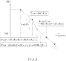
- FIG. 3 is a diagram illustrating a detailed frequency response curve of the amplifier circuit 100 shown in FIG. 1 according to an embodiment of the present invention.
- the aforementioned dominant pole P 1 is denoted by P 1,LHP in FIG. 3
- the aforementioned non-dominant pole P d is denoted by P 2,LHP in FIG. 3
- the aforementioned zero Z d is denoted by Z 1,LHP in FIG. 3 .
- the inserted zero Z 1,LHP is mainly controlled by capacitance of the capacitor C d2 and resistance of the resistor R d2
- the inserted non-dominant pole P 2,LHP is at least controlled by capacitance of the capacitor C d1 , capacitance of the capacitor C d2 and resistance of the resistor R d2 .
- the shrink factor k depends on capacitance of capacitor C d1 , capacitance of compensation capacitor C m1 , resistance of resistor R d2 , and transconductance G m2 of second-stage amplifier 116.
- the shrink factor k can be set by a value larger than one (i.e., k>1) for stability enhancement, and can be precisely controlled by capacitance of capacitor C d1 , capacitance of compensation capacitor C m1 , resistance of resistor R d2 , and transconductance G m2 of second-stage amplifier 116.
- the shrink factor k should be controlled to provide enough in-band phase margin (PM) for making the amplifier circuit 100 unconditionally stable in a closed-loop operation.
- PM in-band phase margin
- the shrink factor k may be set by a value less than 10 (i.e., k ⁇ 10) to make the in-band PM larger than 35 degrees.
- k ⁇ 10 a value less than 10
- one high-frequency non-dominant pole P 3,LHP depends on the capacitance of the compensation capacitor C m2 and the resistance of the resistor R d2
- another zero (e.g., high-frequency zero) Z 2,LHP depends on the capacitance of the capacitor C d1 and the resistance of the resistor R d1 .
- the high-frequency non-dominant pole P 3,LHP may be cancelled by the high-frequency zero Z 2,LHP .
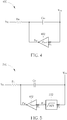
- FIG. 4 is a diagram illustrating a first compensation circuit design according to an embodiment of the present invention.
- the compensation circuit 400 includes an auxiliary amplifier 402 with transconductance G md1 , a capacitor C B1 , and a resistor R B .
- the gain of the auxiliary amplifier 402 is negative.
- An input port P 41 of the auxiliary amplifier 402 is coupled to an input V IN of the compensation circuit 400.
- the capacitor C B1 is coupled between the input port P 41 and the output port P 42 of the auxiliary amplifier 402.
- the resistor R B1 is coupled between the output port P 42 of the auxiliary amplifier 402 and a bias voltage V B1 (e.g., a ground voltage) .
- V B1 bias voltage
- the compensation circuit 400 has high input impedance due to the fact that the input V IN of the compensation circuit 400 is coupled to the input port P 41 of the auxiliary amplifier 402 (e.g., a gate of an input transistor in the auxiliary amplifier 402).
- the auxiliary amplifier 402 e.g., a gate of an input transistor in the auxiliary amplifier 402
- high impedance is required at an output of the first-stage amplifier 114 (i.e., an input of the second-stage amplifier 116) for low noise injection.
- the first compensation circuit 104_1 may be implemented using the compensation circuit 400 shown in FIG. 4 , where the input V IN of the compensation circuit 400 is coupled to the output port P 12 of the first-stage amplifier 114.
- the compensation circuit 400 uses a capacitance multiplication technique. Hence, the compensation circuit 400 may be regarded as having capacitance equal to G md1 *C B1 *R B1 . In addition, the compensation circuit 400 may be regarded as having resistance equal to 1 G md 1 .
- the transconductance G md1 of the auxiliary amplifier 402 may be set by a large value to make the capacitor C d1 has a large capacitance value.
- the compensation circuit 400 may fail to perform the capacitance multiplication function, needed by the first compensation circuit 104_1 when the in-band signal swing at the input V IN of the compensation circuit 400 exceeds a small signal range of the auxiliary amplifier 402 with large transconductance G md1 .
- the present invention proposes another compensation circuit design with a high-pass filter (HPF) added to the compensation circuit 400 shown in FIG. 4 .
- HPF high-pass filter
- FIG. 5 is a diagram illustrating a second compensation circuit design according to an embodiment of the present invention.
- the compensation circuit 500 has a high-pass filter (HPF) 502 included therein, where an input port P 51 of the HPF 502 is coupled to the input V IN of the compensation circuit 500, and an output port P 52 of the HPF 502 is coupled to the input port P 41 of the auxiliary amplifier 402.
- HPF high-pass filter
- An in-band signal with a large swing may be attenuated by the HPF 502 to fall within the small signal range of the auxiliary amplifier 402 with large transconductance G md1 .
- the compensation circuit 500 has high input impedance due to the fact that the input V IN of the compensation circuit 400 is coupled to the input port P41 of the auxiliary amplifier 402 via the HPF 502.
- high impedance is required at an output of the first-stage amplifier 114 (i.e., an input of the second-stage amplifier 116) for low noise injection.
- the first compensation circuit 104_1 may be implemented using the compensation circuit 500 shown in FIG. 5 , where the input V IN of the compensation circuit 500 is coupled to the output port P 12 of the first-stage amplifier 114.
- the compensation circuit 500 is required to have the HPF 502 located in a loop formed by the auxiliary amplifier 402 and the capacitor C B1 .
- FIG. 6 is a diagram illustrating a compensation circuit with an HPF located outside of a loop formed by an auxiliary amplifier and a capacitor.
- FIG. 7 is a diagram illustrating a compensation circuit with an HPF located in a loop formed by an auxiliary amplifier and a capacitor. As shown in FIG. 6 , the compensation circuit 600 has the HPF 502 located outside of the loop formed by the auxiliary amplifier 402 and the capacitor C B1 .
- the capacitance C d1A looking into the auxiliary amplifier 402 is G md1 *R B1 *C B1
- the resistance R d1A looking into the auxiliary amplifier 402 is 1 G md 1 .
- the HPF 502 may be implemented using a resistor R F1 and a capacitor C F1 . Since the HPF 502 is located outside of the loop formed by the auxiliary amplifier 402 and the capacitor C B1 , the capacitance C d1 looking into the HPF 502 is C d1A ⁇ C F1 , and the resistance R d1 looking into the HPF 502 is R d1A
- the compensation circuit 500 has the HPF 502 located in the loop formed by the auxiliary amplifier 402 and the capacitor C B1 .
- the HPF 502 may be implemented using the resistor R F1 and the capacitor C F1 . Since the HPF 502 is located in the loop formed by the auxiliary amplifier 402 and the capacitor C B1 , the capacitance C d1 looking into the HPF 502 is G md1 (HPF) *R B1 *C B1 , and the resistance R d1 looking into the HPF 502 is 1 G md 1 HPF .
- both of the equivalent capacitor G md1 (HPF) *R B1 *C B1 and equivalent resistor 1 G md 1 HPF are open-circuited.
- the compensation circuit 500 present an amplified capacitance of G md1 (HPF) *R B1 *C B1 to control the unity-gain bandwidth. There is no load effect jeopardizing the capacitance multiplication operation.
- FIG. 8 is a circuit diagram of the compensation circuit 500 shown in FIG. 5 / FIG. 7 according to an embodiment of the present invention.
- one end of the capacitor C B1 and one end of the capacitor C F1 are both coupled to the input V IN
- another end of the capacitor C F1 is coupled to a gate of an input transistor of the auxiliary amplifier 402
- another end of the capacitor C B1 is coupled to a drain of an output transistor of the auxiliary amplifier 402.
- the HPF 502 is located in the loop formed by the capacitor C B1 and the auxiliary amplifier 402, thus avoiding the load effect.
- the circuit design of the auxiliary amplifier 402 shown in FIG. 8 is for illustrative purposes only, and is not meant to be a limitation of the present invention. That is, in some embodiments of the present invention, the auxiliary amplifier 402 may be implemented using a circuit design different from that shown in FIG. 8 .
- FIG. 9 is a diagram illustrating a third compensation circuit design according to an embodiment of the present invention.
- the compensation circuit 900 includes an auxiliary amplifier 902 with transconductance G md2 , a capacitor C B2 , and a resistor R B2 .
- the gain of the auxiliary amplifier 902 is negative.
- An output port P 92 of the auxiliary amplifier 902 is coupled to an input V IN of the compensation circuit 900.
- the capacitor C B2 is coupled between the input port P 91 and an output port P 92 of the auxiliary amplifier 902.
- the resistor R B2 is coupled between the input port P 91 of the auxiliary amplifier 902 and a bias voltage V B2 (e.g., a ground voltage) .
- V B2 bias voltage
- the compensation circuit 900 is suitable for a large-swing signal at the input V IN of the compensation circuit 900.
- an output of the second-stage amplifier 116 (which is also an input of the third-stage amplifier 118) may have a large swing for Class-AB operation.
- the second compensation circuit 104_2 may be implemented using the compensation circuit 900 shown in FIG. 9 , where the input V IN of the compensation circuit 900 is coupled to the output port P 22 of the second-stage amplifier 116.
- this is for illustrative purposes only, and is not meant to be a limitation of the present invention.
- the second compensation circuit 104_2 may be implemented using the compensation circuit 400/500, such that the output of the second-stage amplifier 116 (which is also the input of the third-stage amplifier 118) may benefit from the high impedance offered by the compensation circuit 400/500.
- the multi-stage amplifier used in the amplifier circuit 100 is a three-stage amplifier. However, the same frequency response (unity-gain-bandwidth control) scheme can be extended and applied to a multi-stage amplifier having more than three amplifier stages.
- FIG. 10 is a diagram illustrating another amplifier circuit according to an embodiment of the present invention. By way of example, but not limitation, the amplifier circuit 1000 may be used in an audio application. As shown in FIG.
- the amplifier circuit 100 is a multi-stage amplifier circuit including an N-stage amplifier composed of amplifiers AMP 1 -AMP N , (N-1) compensation circuits CMP 1 -CMP N-1 , and (N-1) compensation capacitors C m1 -C m(N-1) , where N is a positive integer larger than 3 (i.e., N>3) .
- N is a positive integer larger than 3 (i.e., N>3) .
- Each of the compensation capacitors C m1 -C m(N-1) is used for Miller compensation.
- the compensation capacitors C m2 -C m(N-1) are optional.
- the compensation capacitors C m2 -C m(N-1) can be omitted, depending upon the actual design considerations.
- the compensation circuit CMP 1 may be implemented using the compensation circuit 400/500.
- Each of the compensation circuits CMP 2 -CMP N-1 may be implemented using one of the compensation circuits 400, 500 and 900, depending upon the actual design considerations.
- at least one zero and at least one pole can be inserted by compensation circuits CMP 1 -CMP N-1 . In this way, the amplifier circuit 100 can have enhanced stability without in-band gain degradation.
Landscapes
- Engineering & Computer Science (AREA)
- Power Engineering (AREA)
- Amplifiers (AREA)
Applications Claiming Priority (2)
| Application Number | Priority Date | Filing Date | Title |
|---|---|---|---|
| US201762487013P | 2017-04-19 | 2017-04-19 | |
| US15/912,448 US10469037B2 (en) | 2017-04-19 | 2018-03-05 | Multi-stage amplifier circuit with zero and pole inserted by compensation circuits |
Publications (3)
| Publication Number | Publication Date |
|---|---|
| EP3402069A2 true EP3402069A2 (de) | 2018-11-14 |
| EP3402069A3 EP3402069A3 (de) | 2019-05-22 |
| EP3402069B1 EP3402069B1 (de) | 2021-05-26 |
Family
ID=61731589
Family Applications (1)
| Application Number | Title | Priority Date | Filing Date |
|---|---|---|---|
| EP18162836.3A Active EP3402069B1 (de) | 2017-04-19 | 2018-03-20 | Mehrstufige verstärkerschaltung mit null- und pol-einsatz durch kompensationsschaltungen |
Country Status (2)
| Country | Link |
|---|---|
| US (1) | US10469037B2 (de) |
| EP (1) | EP3402069B1 (de) |
Families Citing this family (4)
| Publication number | Priority date | Publication date | Assignee | Title |
|---|---|---|---|---|
| US11196387B2 (en) | 2019-05-28 | 2021-12-07 | Mediatek Inc. | Amplifier circuit with high-order damping circuit and the high-order damping circuit |
| CN114629456B (zh) * | 2020-12-10 | 2024-10-15 | 圣邦微电子(北京)股份有限公司 | 输出级电路和ab类放大器 |
| US12627272B2 (en) * | 2021-05-20 | 2026-05-12 | The Royal Institution For The Advancement Of Learning/Mcgill University | Enhanced gain of operational amplifiers through low-frequency zero positioning |
| TWI890265B (zh) * | 2024-01-10 | 2025-07-11 | 茂達電子股份有限公司 | 實現等效放大電容值的補償電路 |
Family Cites Families (15)
| Publication number | Priority date | Publication date | Assignee | Title |
|---|---|---|---|---|
| US1784857A (en) * | 1925-08-25 | 1930-12-16 | Rca Corp | Electron-tube circuits |
| US6150884A (en) | 1998-05-13 | 2000-11-21 | Texas Instruments Incorporated | Multistage amplifier circuit with improved nested transconductance capacitance compensation |
| US6208206B1 (en) * | 1999-02-11 | 2001-03-27 | The Hong Kong University Of Science And Technology | Frequency compensation techniques for low-power multistage amplifiers |
| DE10031522B9 (de) | 2000-06-28 | 2007-07-12 | Infineon Technologies Ag | Frequenzkompensierte Verstärkeranordnung und Verfahren zum Betrieb einer frequenzkompensierten Verstärkeranordnung |
| US7495422B2 (en) | 2005-07-22 | 2009-02-24 | Hong Kong University Of Science And Technology | Area-efficient capacitor-free low-dropout regulator |
| US7459972B2 (en) | 2005-11-02 | 2008-12-02 | Marvell World Trade Ltd. | Amplifiers with compensation |
| KR101278951B1 (ko) | 2006-05-24 | 2013-06-26 | 페어차일드코리아반도체 주식회사 | 혼합형 주파수 보상회로, 제어회로, dc-dc 컨버터 및 이들의 제어 방법 |
| US20110234312A1 (en) | 2010-03-24 | 2011-09-29 | Texas Instruments Incorporated | Amplifier with improved stability |
| EP2759899A1 (de) | 2013-01-25 | 2014-07-30 | Dialog Semiconductor GmbH | Sauberes Starten und Stromsparen bei der gepulsten LDO-Aktivierung |
| US8963639B2 (en) | 2013-02-19 | 2015-02-24 | University Of Macau | Frequency compensation techniques for low-power and small-area multistage amplifiers |
| US9634617B2 (en) | 2014-07-02 | 2017-04-25 | Texas Instruments Incorporated | Multistage amplifier circuit with improved settling time |
| US9979350B2 (en) | 2014-11-17 | 2018-05-22 | Mediatek Inc. | Operational amplifier based circuit with compensation circuit block used for stability compensation |
| US9768740B2 (en) | 2015-02-02 | 2017-09-19 | Skyworks Solutions, Inc. | Feedback compensation for multistage amplifiers |
| CN104734646B (zh) | 2015-04-13 | 2018-11-23 | 无锡新硅微电子有限公司 | 应用于多级放大电路的单米勒电容频率补偿方法 |
| US9680420B2 (en) | 2015-09-29 | 2017-06-13 | Silicon Laboratories Inc. | Apparatus for compensation of electronic circuitry and associated methods |
-
2018
- 2018-03-05 US US15/912,448 patent/US10469037B2/en active Active
- 2018-03-20 EP EP18162836.3A patent/EP3402069B1/de active Active
Non-Patent Citations (1)
| Title |
|---|
| None |
Also Published As
| Publication number | Publication date |
|---|---|
| EP3402069A3 (de) | 2019-05-22 |
| US10469037B2 (en) | 2019-11-05 |
| US20180309416A1 (en) | 2018-10-25 |
| EP3402069B1 (de) | 2021-05-26 |
Similar Documents
| Publication | Publication Date | Title |
|---|---|---|
| EP3402069B1 (de) | Mehrstufige verstärkerschaltung mit null- und pol-einsatz durch kompensationsschaltungen | |
| US7973605B2 (en) | Three-stage frequency-compensated operational amplifier for driving large capacitive loads | |
| US7551033B2 (en) | Dynamic bandwidth compensating method and associated apparatus | |
| CN110233600B (zh) | 放大器电路及补偿电路 | |
| US11901868B2 (en) | Amplifier circuit, adder circuit, reception circuit, and integrated circuit | |
| CN108141188A (zh) | 具有提升的峰化的放大器 | |
| US11196387B2 (en) | Amplifier circuit with high-order damping circuit and the high-order damping circuit | |
| US7292098B2 (en) | Operational amplifier | |
| US20220263480A1 (en) | Operational amplifier using single-stage amplifier with slew-rate enhancement and associated method | |
| WO2017098580A1 (ja) | 高周波多段増幅器 | |
| US10833643B1 (en) | Method and structure for controlling bandwidth and peaking over gain in a variable gain amplifier (VGA) | |
| CN103534936B (zh) | 电流缓冲器 | |
| US20150270816A1 (en) | Performance of off-chip connection for power amplifier | |
| US20130293304A1 (en) | Compensation technique for feedback amplifiers | |
| CN109120232A (zh) | 适用于低噪声、宽动态范围的高带宽跨阻放大器 | |
| US20250175131A1 (en) | Audio amplifier with high pass filter based distortion suppression | |
| KR102857092B1 (ko) | 광대역 고선형성의 가변 이득 증폭기 및 그 방법 | |
| EP3355471B1 (de) | Klasse-ab-verstärker mit kaskodenstufe mit filter zur verbesserung der linearität | |
| EP4175175A1 (de) | Schaltung zur korrektur von arbeitszyklus- und phasenfehlern | |
| JPH0779216B2 (ja) | 高周波増幅装置 | |
| KR102857053B1 (ko) | 초고주파 대역 증폭기 | |
| US20250183856A1 (en) | Output load aware compensation scheme for multi-stage amplifier | |
| KR101907644B1 (ko) | 적응형 이퀄라이징 회로 | |
| WO2025243358A1 (ja) | 多段増幅器 | |
| US20070236288A1 (en) | Apparatus for amplifying differential signal |
Legal Events
| Date | Code | Title | Description |
|---|---|---|---|
| PUAI | Public reference made under article 153(3) epc to a published international application that has entered the european phase |
Free format text: ORIGINAL CODE: 0009012 |
|
| STAA | Information on the status of an ep patent application or granted ep patent |
Free format text: STATUS: THE APPLICATION HAS BEEN PUBLISHED |
|
| AK | Designated contracting states |
Kind code of ref document: A2 Designated state(s): AL AT BE BG CH CY CZ DE DK EE ES FI FR GB GR HR HU IE IS IT LI LT LU LV MC MK MT NL NO PL PT RO RS SE SI SK SM TR |
|
| AX | Request for extension of the european patent |
Extension state: BA ME |
|
| PUAL | Search report despatched |
Free format text: ORIGINAL CODE: 0009013 |
|
| AK | Designated contracting states |
Kind code of ref document: A3 Designated state(s): AL AT BE BG CH CY CZ DE DK EE ES FI FR GB GR HR HU IE IS IT LI LT LU LV MC MK MT NL NO PL PT RO RS SE SI SK SM TR |
|
| AX | Request for extension of the european patent |
Extension state: BA ME |
|
| RIC1 | Information provided on ipc code assigned before grant |
Ipc: H03F 1/08 20060101ALI20190415BHEP Ipc: H03F 1/14 20060101AFI20190415BHEP Ipc: H03F 1/34 20060101ALI20190415BHEP Ipc: H03F 3/21 20060101ALI20190415BHEP |
|
| STAA | Information on the status of an ep patent application or granted ep patent |
Free format text: STATUS: REQUEST FOR EXAMINATION WAS MADE |
|
| 17P | Request for examination filed |
Effective date: 20191120 |
|
| RBV | Designated contracting states (corrected) |
Designated state(s): AL AT BE BG CH CY CZ DE DK EE ES FI FR GB GR HR HU IE IS IT LI LT LU LV MC MK MT NL NO PL PT RO RS SE SI SK SM TR |
|
| STAA | Information on the status of an ep patent application or granted ep patent |
Free format text: STATUS: EXAMINATION IS IN PROGRESS |
|
| 17Q | First examination report despatched |
Effective date: 20200220 |
|
| GRAP | Despatch of communication of intention to grant a patent |
Free format text: ORIGINAL CODE: EPIDOSNIGR1 |
|
| STAA | Information on the status of an ep patent application or granted ep patent |
Free format text: STATUS: GRANT OF PATENT IS INTENDED |
|
| RAP1 | Party data changed (applicant data changed or rights of an application transferred) |
Owner name: MEDIATEK INC. |
|
| INTG | Intention to grant announced |
Effective date: 20201215 |
|
| RIN1 | Information on inventor provided before grant (corrected) |
Inventor name: WEN, SUNG-HAN Inventor name: CHEN, KUAN-TA |
|
| GRAS | Grant fee paid |
Free format text: ORIGINAL CODE: EPIDOSNIGR3 |
|
| GRAA | (expected) grant |
Free format text: ORIGINAL CODE: 0009210 |
|
| STAA | Information on the status of an ep patent application or granted ep patent |
Free format text: STATUS: THE PATENT HAS BEEN GRANTED |
|
| AK | Designated contracting states |
Kind code of ref document: B1 Designated state(s): AL AT BE BG CH CY CZ DE DK EE ES FI FR GB GR HR HU IE IS IT LI LT LU LV MC MK MT NL NO PL PT RO RS SE SI SK SM TR |
|
| REG | Reference to a national code |
Ref country code: GB Ref legal event code: FG4D |
|
| REG | Reference to a national code |
Ref country code: CH Ref legal event code: EP |
|
| REG | Reference to a national code |
Ref country code: DE Ref legal event code: R096 Ref document number: 602018017509 Country of ref document: DE |
|
| REG | Reference to a national code |
Ref country code: AT Ref legal event code: REF Ref document number: 1397256 Country of ref document: AT Kind code of ref document: T Effective date: 20210615 |
|
| REG | Reference to a national code |
Ref country code: IE Ref legal event code: FG4D |
|
| REG | Reference to a national code |
Ref country code: LT Ref legal event code: MG9D |
|
| REG | Reference to a national code |
Ref country code: AT Ref legal event code: MK05 Ref document number: 1397256 Country of ref document: AT Kind code of ref document: T Effective date: 20210526 |
|
| PG25 | Lapsed in a contracting state [announced via postgrant information from national office to epo] |
Ref country code: FI Free format text: LAPSE BECAUSE OF FAILURE TO SUBMIT A TRANSLATION OF THE DESCRIPTION OR TO PAY THE FEE WITHIN THE PRESCRIBED TIME-LIMIT Effective date: 20210526 Ref country code: LT Free format text: LAPSE BECAUSE OF FAILURE TO SUBMIT A TRANSLATION OF THE DESCRIPTION OR TO PAY THE FEE WITHIN THE PRESCRIBED TIME-LIMIT Effective date: 20210526 Ref country code: BG Free format text: LAPSE BECAUSE OF FAILURE TO SUBMIT A TRANSLATION OF THE DESCRIPTION OR TO PAY THE FEE WITHIN THE PRESCRIBED TIME-LIMIT Effective date: 20210826 Ref country code: AT Free format text: LAPSE BECAUSE OF FAILURE TO SUBMIT A TRANSLATION OF THE DESCRIPTION OR TO PAY THE FEE WITHIN THE PRESCRIBED TIME-LIMIT Effective date: 20210526 Ref country code: HR Free format text: LAPSE BECAUSE OF FAILURE TO SUBMIT A TRANSLATION OF THE DESCRIPTION OR TO PAY THE FEE WITHIN THE PRESCRIBED TIME-LIMIT Effective date: 20210526 |
|
| REG | Reference to a national code |
Ref country code: NL Ref legal event code: MP Effective date: 20210526 |
|
| PG25 | Lapsed in a contracting state [announced via postgrant information from national office to epo] |
Ref country code: GR Free format text: LAPSE BECAUSE OF FAILURE TO SUBMIT A TRANSLATION OF THE DESCRIPTION OR TO PAY THE FEE WITHIN THE PRESCRIBED TIME-LIMIT Effective date: 20210827 Ref country code: IS Free format text: LAPSE BECAUSE OF FAILURE TO SUBMIT A TRANSLATION OF THE DESCRIPTION OR TO PAY THE FEE WITHIN THE PRESCRIBED TIME-LIMIT Effective date: 20210926 Ref country code: RS Free format text: LAPSE BECAUSE OF FAILURE TO SUBMIT A TRANSLATION OF THE DESCRIPTION OR TO PAY THE FEE WITHIN THE PRESCRIBED TIME-LIMIT Effective date: 20210526 Ref country code: SE Free format text: LAPSE BECAUSE OF FAILURE TO SUBMIT A TRANSLATION OF THE DESCRIPTION OR TO PAY THE FEE WITHIN THE PRESCRIBED TIME-LIMIT Effective date: 20210526 Ref country code: PT Free format text: LAPSE BECAUSE OF FAILURE TO SUBMIT A TRANSLATION OF THE DESCRIPTION OR TO PAY THE FEE WITHIN THE PRESCRIBED TIME-LIMIT Effective date: 20210927 Ref country code: PL Free format text: LAPSE BECAUSE OF FAILURE TO SUBMIT A TRANSLATION OF THE DESCRIPTION OR TO PAY THE FEE WITHIN THE PRESCRIBED TIME-LIMIT Effective date: 20210526 Ref country code: NO Free format text: LAPSE BECAUSE OF FAILURE TO SUBMIT A TRANSLATION OF THE DESCRIPTION OR TO PAY THE FEE WITHIN THE PRESCRIBED TIME-LIMIT Effective date: 20210826 Ref country code: LV Free format text: LAPSE BECAUSE OF FAILURE TO SUBMIT A TRANSLATION OF THE DESCRIPTION OR TO PAY THE FEE WITHIN THE PRESCRIBED TIME-LIMIT Effective date: 20210526 |
|
| PG25 | Lapsed in a contracting state [announced via postgrant information from national office to epo] |
Ref country code: NL Free format text: LAPSE BECAUSE OF FAILURE TO SUBMIT A TRANSLATION OF THE DESCRIPTION OR TO PAY THE FEE WITHIN THE PRESCRIBED TIME-LIMIT Effective date: 20210526 |
|
| PG25 | Lapsed in a contracting state [announced via postgrant information from national office to epo] |
Ref country code: EE Free format text: LAPSE BECAUSE OF FAILURE TO SUBMIT A TRANSLATION OF THE DESCRIPTION OR TO PAY THE FEE WITHIN THE PRESCRIBED TIME-LIMIT Effective date: 20210526 Ref country code: ES Free format text: LAPSE BECAUSE OF FAILURE TO SUBMIT A TRANSLATION OF THE DESCRIPTION OR TO PAY THE FEE WITHIN THE PRESCRIBED TIME-LIMIT Effective date: 20210526 Ref country code: SK Free format text: LAPSE BECAUSE OF FAILURE TO SUBMIT A TRANSLATION OF THE DESCRIPTION OR TO PAY THE FEE WITHIN THE PRESCRIBED TIME-LIMIT Effective date: 20210526 Ref country code: SM Free format text: LAPSE BECAUSE OF FAILURE TO SUBMIT A TRANSLATION OF THE DESCRIPTION OR TO PAY THE FEE WITHIN THE PRESCRIBED TIME-LIMIT Effective date: 20210526 Ref country code: RO Free format text: LAPSE BECAUSE OF FAILURE TO SUBMIT A TRANSLATION OF THE DESCRIPTION OR TO PAY THE FEE WITHIN THE PRESCRIBED TIME-LIMIT Effective date: 20210526 Ref country code: DK Free format text: LAPSE BECAUSE OF FAILURE TO SUBMIT A TRANSLATION OF THE DESCRIPTION OR TO PAY THE FEE WITHIN THE PRESCRIBED TIME-LIMIT Effective date: 20210526 Ref country code: CZ Free format text: LAPSE BECAUSE OF FAILURE TO SUBMIT A TRANSLATION OF THE DESCRIPTION OR TO PAY THE FEE WITHIN THE PRESCRIBED TIME-LIMIT Effective date: 20210526 |
|
| REG | Reference to a national code |
Ref country code: DE Ref legal event code: R097 Ref document number: 602018017509 Country of ref document: DE |
|
| PLBE | No opposition filed within time limit |
Free format text: ORIGINAL CODE: 0009261 |
|
| STAA | Information on the status of an ep patent application or granted ep patent |
Free format text: STATUS: NO OPPOSITION FILED WITHIN TIME LIMIT |
|
| 26N | No opposition filed |
Effective date: 20220301 |
|
| PG25 | Lapsed in a contracting state [announced via postgrant information from national office to epo] |
Ref country code: IS Free format text: LAPSE BECAUSE OF FAILURE TO SUBMIT A TRANSLATION OF THE DESCRIPTION OR TO PAY THE FEE WITHIN THE PRESCRIBED TIME-LIMIT Effective date: 20210926 Ref country code: AL Free format text: LAPSE BECAUSE OF FAILURE TO SUBMIT A TRANSLATION OF THE DESCRIPTION OR TO PAY THE FEE WITHIN THE PRESCRIBED TIME-LIMIT Effective date: 20210526 |
|
| PG25 | Lapsed in a contracting state [announced via postgrant information from national office to epo] |
Ref country code: IT Free format text: LAPSE BECAUSE OF FAILURE TO SUBMIT A TRANSLATION OF THE DESCRIPTION OR TO PAY THE FEE WITHIN THE PRESCRIBED TIME-LIMIT Effective date: 20210526 |
|
| PG25 | Lapsed in a contracting state [announced via postgrant information from national office to epo] |
Ref country code: MC Free format text: LAPSE BECAUSE OF FAILURE TO SUBMIT A TRANSLATION OF THE DESCRIPTION OR TO PAY THE FEE WITHIN THE PRESCRIBED TIME-LIMIT Effective date: 20210526 |
|
| REG | Reference to a national code |
Ref country code: CH Ref legal event code: PL |
|
| REG | Reference to a national code |
Ref country code: BE Ref legal event code: MM Effective date: 20220331 |
|
| PG25 | Lapsed in a contracting state [announced via postgrant information from national office to epo] |
Ref country code: LU Free format text: LAPSE BECAUSE OF NON-PAYMENT OF DUE FEES Effective date: 20220320 Ref country code: LI Free format text: LAPSE BECAUSE OF NON-PAYMENT OF DUE FEES Effective date: 20220331 Ref country code: IE Free format text: LAPSE BECAUSE OF NON-PAYMENT OF DUE FEES Effective date: 20220320 Ref country code: CH Free format text: LAPSE BECAUSE OF NON-PAYMENT OF DUE FEES Effective date: 20220331 |
|
| PG25 | Lapsed in a contracting state [announced via postgrant information from national office to epo] |
Ref country code: BE Free format text: LAPSE BECAUSE OF NON-PAYMENT OF DUE FEES Effective date: 20220331 |
|
| P01 | Opt-out of the competence of the unified patent court (upc) registered |
Effective date: 20230607 |
|
| PG25 | Lapsed in a contracting state [announced via postgrant information from national office to epo] |
Ref country code: HU Free format text: LAPSE BECAUSE OF FAILURE TO SUBMIT A TRANSLATION OF THE DESCRIPTION OR TO PAY THE FEE WITHIN THE PRESCRIBED TIME-LIMIT; INVALID AB INITIO Effective date: 20180320 |
|
| PG25 | Lapsed in a contracting state [announced via postgrant information from national office to epo] |
Ref country code: MK Free format text: LAPSE BECAUSE OF FAILURE TO SUBMIT A TRANSLATION OF THE DESCRIPTION OR TO PAY THE FEE WITHIN THE PRESCRIBED TIME-LIMIT Effective date: 20210526 Ref country code: CY Free format text: LAPSE BECAUSE OF FAILURE TO SUBMIT A TRANSLATION OF THE DESCRIPTION OR TO PAY THE FEE WITHIN THE PRESCRIBED TIME-LIMIT Effective date: 20210526 |
|
| PG25 | Lapsed in a contracting state [announced via postgrant information from national office to epo] |
Ref country code: MT Free format text: LAPSE BECAUSE OF FAILURE TO SUBMIT A TRANSLATION OF THE DESCRIPTION OR TO PAY THE FEE WITHIN THE PRESCRIBED TIME-LIMIT Effective date: 20210526 |
|
| PG25 | Lapsed in a contracting state [announced via postgrant information from national office to epo] |
Ref country code: TR Free format text: LAPSE BECAUSE OF FAILURE TO SUBMIT A TRANSLATION OF THE DESCRIPTION OR TO PAY THE FEE WITHIN THE PRESCRIBED TIME-LIMIT Effective date: 20210526 |
|
| PGFP | Annual fee paid to national office [announced via postgrant information from national office to epo] |
Ref country code: FR Payment date: 20251231 Year of fee payment: 9 |
|
| PGFP | Annual fee paid to national office [announced via postgrant information from national office to epo] |
Ref country code: GB Payment date: 20260106 Year of fee payment: 9 |
|
| PGFP | Annual fee paid to national office [announced via postgrant information from national office to epo] |
Ref country code: DE Payment date: 20260102 Year of fee payment: 9 |