EP3401725A1 - Transparent optical coupler active matrix array - Google Patents
Transparent optical coupler active matrix array Download PDFInfo
- Publication number
- EP3401725A1 EP3401725A1 EP18166832.8A EP18166832A EP3401725A1 EP 3401725 A1 EP3401725 A1 EP 3401725A1 EP 18166832 A EP18166832 A EP 18166832A EP 3401725 A1 EP3401725 A1 EP 3401725A1
- Authority
- EP
- European Patent Office
- Prior art keywords
- light
- backplane
- wavelength
- sensing
- control
- Prior art date
- Legal status (The legal status is an assumption and is not a legal conclusion. Google has not performed a legal analysis and makes no representation as to the accuracy of the status listed.)
- Pending
Links
Images


Classifications
-
- G—PHYSICS
- G01—MEASURING; TESTING
- G01N—INVESTIGATING OR ANALYSING MATERIALS BY DETERMINING THEIR CHEMICAL OR PHYSICAL PROPERTIES
- G01N21/00—Investigating or analysing materials by the use of optical means, i.e. using sub-millimetre waves, infrared, visible or ultraviolet light
- G01N21/84—Systems specially adapted for particular applications
- G01N21/88—Investigating the presence of flaws or contamination
-
- G—PHYSICS
- G02—OPTICS
- G02B—OPTICAL ELEMENTS, SYSTEMS OR APPARATUS
- G02B27/00—Optical systems or apparatus not provided for by any of the groups G02B1/00 - G02B26/00, G02B30/00
- G02B27/10—Beam splitting or combining systems
- G02B27/14—Beam splitting or combining systems operating by reflection only
- G02B27/141—Beam splitting or combining systems operating by reflection only using dichroic mirrors
-
- H—ELECTRICITY
- H04—ELECTRIC COMMUNICATION TECHNIQUE
- H04N—PICTORIAL COMMUNICATION, e.g. TELEVISION
- H04N23/00—Cameras or camera modules comprising electronic image sensors; Control thereof
- H04N23/20—Cameras or camera modules comprising electronic image sensors; Control thereof for generating image signals from infrared radiation only
- H04N23/21—Cameras or camera modules comprising electronic image sensors; Control thereof for generating image signals from infrared radiation only from near infrared [NIR] radiation
-
- H—ELECTRICITY
- H10—SEMICONDUCTOR DEVICES; ELECTRIC SOLID-STATE DEVICES NOT OTHERWISE PROVIDED FOR
- H10D—INORGANIC ELECTRIC SEMICONDUCTOR DEVICES
- H10D86/00—Integrated devices formed in or on insulating or conducting substrates, e.g. formed in silicon-on-insulator [SOI] substrates or on stainless steel or glass substrates
- H10D86/40—Integrated devices formed in or on insulating or conducting substrates, e.g. formed in silicon-on-insulator [SOI] substrates or on stainless steel or glass substrates characterised by multiple TFTs
- H10D86/60—Integrated devices formed in or on insulating or conducting substrates, e.g. formed in silicon-on-insulator [SOI] substrates or on stainless steel or glass substrates characterised by multiple TFTs wherein the TFTs are in active matrices
-
- H—ELECTRICITY
- H10—SEMICONDUCTOR DEVICES; ELECTRIC SOLID-STATE DEVICES NOT OTHERWISE PROVIDED FOR
- H10F—INORGANIC SEMICONDUCTOR DEVICES SENSITIVE TO INFRARED RADIATION, LIGHT, ELECTROMAGNETIC RADIATION OF SHORTER WAVELENGTH OR CORPUSCULAR RADIATION
- H10F30/00—Individual radiation-sensitive semiconductor devices in which radiation controls the flow of current through the devices, e.g. photodetectors
- H10F30/20—Individual radiation-sensitive semiconductor devices in which radiation controls the flow of current through the devices, e.g. photodetectors the devices having potential barriers, e.g. phototransistors
- H10F30/21—Individual radiation-sensitive semiconductor devices in which radiation controls the flow of current through the devices, e.g. photodetectors the devices having potential barriers, e.g. phototransistors the devices being sensitive to infrared, visible or ultraviolet radiation
- H10F30/28—Individual radiation-sensitive semiconductor devices in which radiation controls the flow of current through the devices, e.g. photodetectors the devices having potential barriers, e.g. phototransistors the devices being sensitive to infrared, visible or ultraviolet radiation the devices being characterised by field-effect operation, e.g. junction field-effect phototransistors
-
- G—PHYSICS
- G02—OPTICS
- G02B—OPTICAL ELEMENTS, SYSTEMS OR APPARATUS
- G02B27/00—Optical systems or apparatus not provided for by any of the groups G02B1/00 - G02B26/00, G02B30/00
- G02B27/60—Systems using moiré fringes
Definitions
- This disclosure relates to optocoupler arrays, more particularly to optocoupler arrays using active switching matrices.
- Active matrix arrays typically consisting of arrays of transistors, provide access to a large number of electronic elements. These arrays typically address high density light emitting elements such as a liquid crystal display (LCD) or an organic light emitting diode (OLED) display. These active matrix arrays used to access the lighting elements have been made thin to facilitate flat panel displays. Active matrix addressing can also control electronic elements actuated by high voltages. High voltage applications typically involve some type of electrical isolation between control and output circuits.
- LCD liquid crystal display
- OLED organic light emitting diode
- One embodiment consists of a backplane having an array of output terminals arranged on an output surface of the backplane, and an array of solid state optical switches, each optical switch corresponding to one of the output terminals, wherein the solid state optical switches are responsive to light of a control wavelength, wherein the backplane is of a material transparent to light of a sensing wavelength different from the control wavelength.
- Another embodiment consists of an optical system includes a backplane having an array of optocouplers, a projector to generate light of a control wavelength to which the optocouplers are responsive, optics to direct the control light onto the array of optocouplers on a backplane, an imaging system responsive to light of a sensing wavelength, wherein the backplane is at least partially transparent to the sensing wavelength.
- US Patent Publication No. 20160351584 discloses an active matrix back plane having thin film optocouplers.
- the optocouplers, or photo transistors allow for high voltage inputs to be electrically isolated from lower voltage control systems. High voltage outputs enable many different applications such as microelectromechanical system (MEMS) devices and driving certain types of displays like liquid crystal displays.
- MEMS microelectromechanical system
- the term optocoupler or photo transistor refers to an optical switch having a region of photosensitive material that, when exposed to light, generates a voltage that causes the switch to activate.
- a pixelated light source such as a display
- activates the individual lights of the source it actuates the corresponding switches on the backplane to cause the switches to output the high voltage input. This provides the ability to form patterns on the side of the backplane opposite the pixelated light source.
- FIG 1 shows an example of one such application.
- the optocoupler active matrix 12, or OptoCAM has a light source and generates patterns on its surface that take randomly ordered chiplets such as 13 and order them prior to their being deposited on the substrate 16.
- One technique used to provide feedback use vision systems such as video cameras.
- the camera can take one of several positions shown as 18, 20 and 22.
- Position 18 cannot view the chiplets directly underneath the transfer mechanism 14, which is typically not transparent.
- Position 20 allows better coverage of the chiplets, but suffers from shallow oblique angles, resulting in poor image quality.
- Position 22 provides the best position for the most accurate images, except that the OptoCAM backplane blocks the view.
- the publication '584 discusses that the OptoCAM backplane may be transparent. However, to do so becomes logically impossible. Light used to provide illumination to the imaging system would actuate the optical switches in the backplane and change the pattern, for example, in the application shown in Figure 1 . This problem will occur in any system that uses light for whatever purposes, such as the imaging system of Figure 1 .
- the embodiments here separate the control light used to actuate the switches from the imaging or sensing light, which will be referred to here as the sensing light with the understand that it may be both imaging and sensing, or just one or the other.
- the approach here achieves this separation by wavelength.
- the materials in the switches consist of materials transparent at the sensing light wavelength.
- the wavelength and intensity of the sensing light should not induce a specified minimum photo current in the photo transistor.
- the semiconductor has a band gap, such as for crystalline semiconductors, or low density of states energy range that is also considered a band gap, such as amorphous semiconductors. Incident light with energy above the band gap is strongly absorbed; light with energy below the band gap is weakly absorbed, generating an insignificant density of free carriers. Therefore a control illumination should generally have an energy above the band gap energy and a sensing illumination should generally have an energy below the band gap energy.
- Figures 2 and 3 show embodiments of optical switches.
- the electrode, ground plane, and high voltage consist of indium tin oxide (ITO) instead of typical metals.
- Figure 2 shows an element 30, having a source 32 and a drain 34.
- a photosensitive material 36 reacts to the light at the control light, but not at the sensing light wavelength.
- the materials for the source, drain and the layers 38 consist of ITO, and the layers 40 and the small region 42 between the photosensitive material 36 and the drain 34 consist of an oxide or nitride dielectric.
- the photosensitive material consists of amorphous silicon.
- the photo transistor only has 6 layers.
- the photosensitive component 56 consists of a 2000 angstrom thick layer, possibly of amorphous silicon.
- the layers 58 and 59 consist of indium tin oxide.
- layers 58 may have a thickness 1000 angstroms, and layer 59 may have a thickness of 500 angstroms.
- the source 52 may have a thickness of 500 angstroms of ITO, and the drain 54 is at the bottom of layer 58.
- the sensing light has a wavelength in the near infrared (NIR) range, approximately 780 nanometers. At this wavelength the OptoCAM becomes effectively transparent.
- Figures 4 and 5 show different images taken of the OptoCAM device. Figure 4 shows a visible light photo, showing the photosensitive region in the center. Figure 5 shows a line drawn on a piece of paper photographed through the OptoCAM device at NIR wavelengths.
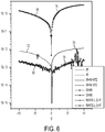
- Figure 6 shows the current-voltage (IV) curves comparison of one photo transistor under dark and flooded with IR light, where IR light includes NIR.
- An on/off ratio that is greater than 100 is achieved even when the device is flooded by IR light.
- the curves are infrared 70, infrared 72, IR plus white that overlays a white light curve 74, curve 76 shows white light and IR plus white light, curve 78 dark and 80 shows dark.
- the control light used to generate these curves was visible white light provided by a typical LCD panel and the sensing light is IR.
- "ON” means that the control light is on and "OFF” means that it is either dark (no light on), or IR.
- the on/off ratio which is the current ratio at the same voltage, improves to even higher values with the use of longer NIR wavelengths such as 880 nanometer light.
- the OptoCAM receives the sensing light continuously.
- the control light could be white or green, with sensing light in the NIR range.
- the OptoCAM may be transparent to multiple wavelengths of light sensing light and/or multiple wavelengths of control light.
- Figure 7 shows an optical system 90.
- the system has a projector 92 with projection optics 94.
- the projector may consist of an array of light emitting elements, such as an array of LCD cells, LEDs, etc.
- the array of LCD cells may be a display panel.
- the control path includes a dichroic mirror 96 and other optical components 98.
- the control light 93 directed to the array of phototransistors in an aligned, image-wise matter, controls the on/off of the phototransistors of the OptoCAM 100.
- the sensing light 103 reflects off the chips, and then reflects off the dichroic filter into the lens of the video camera 102.
- the optical components may include a long pass edge filter to block any control light leakage into the video camera path.
- the video camera path is shown as path 104. In one embodiment, the sensing light can be added at the dichroic mirror 96, then reflected off the assembled objects and collected by the video camera.
- the embodiments assume the use of short wavelengths for control and addressing light, and longer wavelength sensing light.
- any set of orthogonal wavelengths may be used as long as the control light is absorbed by the semiconductor and the control light is not.
- Orthogonal wavelengths do not overlap, so the wavelengths for control and sensing do not overlap.
- the amplitude for sensing is zero.
- the control light may have wavelengths in the red or blue ranges, with sensing light having green or NIR wavelengths.
- Mirrors and filters with well-defined passbands are mature technology and the designer may configure the system to satisfy different requirements.
- the materials used may be modified.
- the phototransistor semiconductor could be replaced with an organic semiconductor, an inorganic oxide based semiconductor such as InGaZnO, etc., or a crystalline semiconductor like GaP (gallium phosphide).
- the ITO layers could be replaced with zinc oxide (ZnO), carbon nanotubes (CNT) networks, etc.
- the materials may be selected, different areas of the arrays may be manufactured from different materials in different regions, or the materials used may have different transparency properties, resulting in a range of transparency for the OptoCAM back plane.
- the OptoCAM could be built with materials opaque to the sensing light occupying less than 50% of the device area, less than 30% of the backplane or device area, or less than 10% of the device area.
- the OptoCAM could have no material opaque to the sensing light, resulting in a device that is effectively completely transparent to the sensing light.
- one or more backplane surfaces are coated with dielectric layers of controlled optical reflectivity at the sensing and control wavelengths
- OptoCAM backplane increases with the ability to separate control light from sensing light.
Landscapes
- Physics & Mathematics (AREA)
- Health & Medical Sciences (AREA)
- General Physics & Mathematics (AREA)
- Signal Processing (AREA)
- Multimedia (AREA)
- Engineering & Computer Science (AREA)
- Toxicology (AREA)
- Optics & Photonics (AREA)
- Life Sciences & Earth Sciences (AREA)
- Immunology (AREA)
- Pathology (AREA)
- General Health & Medical Sciences (AREA)
- Biochemistry (AREA)
- Analytical Chemistry (AREA)
- Chemical & Material Sciences (AREA)
- Solid State Image Pick-Up Elements (AREA)
- Light Receiving Elements (AREA)
- Electroluminescent Light Sources (AREA)
Applications Claiming Priority (1)
| Application Number | Priority Date | Filing Date | Title |
|---|---|---|---|
| US15/582,296 US10397529B2 (en) | 2017-04-28 | 2017-04-28 | Transparent optical coupler active matrix array |
Publications (1)
| Publication Number | Publication Date |
|---|---|
| EP3401725A1 true EP3401725A1 (en) | 2018-11-14 |
Family
ID=61972336
Family Applications (1)
| Application Number | Title | Priority Date | Filing Date |
|---|---|---|---|
| EP18166832.8A Pending EP3401725A1 (en) | 2017-04-28 | 2018-04-11 | Transparent optical coupler active matrix array |
Country Status (3)
| Country | Link |
|---|---|
| US (1) | US10397529B2 (enExample) |
| EP (1) | EP3401725A1 (enExample) |
| JP (1) | JP7073174B2 (enExample) |
Citations (3)
| Publication number | Priority date | Publication date | Assignee | Title |
|---|---|---|---|---|
| KR20090065182A (ko) * | 2007-12-17 | 2009-06-22 | 한국전자통신연구원 | 유기 발광 다이오드 터치스크린 장치 및 그 제조 방법 |
| US20160351584A1 (en) | 2015-05-29 | 2016-12-01 | Palo Alto Research Center Incorporated | Active matrix backplane formed using thin film optocouplers |
| US20170078513A1 (en) * | 2014-03-19 | 2017-03-16 | Bidirectional Display Inc. | Image sensor panel and method for capturing graphical information using same |
Family Cites Families (15)
| Publication number | Priority date | Publication date | Assignee | Title |
|---|---|---|---|---|
| US4779126A (en) | 1983-11-25 | 1988-10-18 | International Rectifier Corporation | Optically triggered lateral thyristor with auxiliary region |
| JPS60193384A (ja) * | 1984-03-15 | 1985-10-01 | Toshiba Corp | 光スイツチングデバイス及び光スイツチング表示装置 |
| KR910007142A (ko) | 1988-09-30 | 1991-04-30 | 미다 가쓰시게 | 박막 광트랜지스터와 그것을 사용한 광센서어레이 |
| US5200634A (en) | 1988-09-30 | 1993-04-06 | Hitachi, Ltd. | Thin film phototransistor and photosensor array using the same |
| US5264720A (en) | 1989-09-22 | 1993-11-23 | Nippondenso Co., Ltd. | High withstanding voltage transistor |
| US5028788A (en) | 1990-04-03 | 1991-07-02 | Electromed International Ltd. | X-ray sensor array |
| US5083175A (en) | 1990-09-21 | 1992-01-21 | Xerox Corporation | Method of using offset gated gap-cell thin film device as a photosensor |
| JP2878137B2 (ja) | 1994-06-29 | 1999-04-05 | シャープ株式会社 | 増幅型光電変換素子、それを用いた増幅型固体撮像装置、及び増幅型光電変換素子の製造方法 |
| US7038242B2 (en) | 2001-02-28 | 2006-05-02 | Agilent Technologies, Inc. | Amorphous semiconductor open base phototransistor array |
| US6885789B2 (en) | 2002-06-07 | 2005-04-26 | Fujitsu Limited | Optical switch fabricated by a thin film process |
| GB0401578D0 (en) | 2004-01-24 | 2004-02-25 | Koninkl Philips Electronics Nv | Phototransistor |
| EP1679749A1 (en) | 2005-01-11 | 2006-07-12 | Ecole Polytechnique Federale De Lausanne Epfl - Sti - Imm - Lmis3 | Semiconductor photodiode and method of making |
| US20140212085A1 (en) | 2013-01-29 | 2014-07-31 | Georgios Margaritis | Optocoupler |
| US9986316B2 (en) * | 2013-08-21 | 2018-05-29 | Telefonaktiebolget Lm Ericsson (Publ) | Optical switching |
| US9946135B2 (en) | 2015-05-29 | 2018-04-17 | Palo Alto Research Center Incorporated | High voltage thin film optical switch |
-
2017
- 2017-04-28 US US15/582,296 patent/US10397529B2/en active Active
-
2018
- 2018-04-04 JP JP2018072211A patent/JP7073174B2/ja active Active
- 2018-04-11 EP EP18166832.8A patent/EP3401725A1/en active Pending
Patent Citations (3)
| Publication number | Priority date | Publication date | Assignee | Title |
|---|---|---|---|---|
| KR20090065182A (ko) * | 2007-12-17 | 2009-06-22 | 한국전자통신연구원 | 유기 발광 다이오드 터치스크린 장치 및 그 제조 방법 |
| US20170078513A1 (en) * | 2014-03-19 | 2017-03-16 | Bidirectional Display Inc. | Image sensor panel and method for capturing graphical information using same |
| US20160351584A1 (en) | 2015-05-29 | 2016-12-01 | Palo Alto Research Center Incorporated | Active matrix backplane formed using thin film optocouplers |
Also Published As
| Publication number | Publication date |
|---|---|
| JP2018190961A (ja) | 2018-11-29 |
| JP7073174B2 (ja) | 2022-05-23 |
| US20180316897A1 (en) | 2018-11-01 |
| US10397529B2 (en) | 2019-08-27 |
Similar Documents
| Publication | Publication Date | Title |
|---|---|---|
| JP7479203B2 (ja) | 発光装置、表示装置、光電変換装置、電子機器、照明装置、移動体およびウェアラブルデバイス | |
| KR102744494B1 (ko) | 디스플레이 장치 | |
| JP2021136208A (ja) | 発光装置、表示装置、露光システム、及び表示撮像装置 | |
| US20080124072A1 (en) | Electric shutter with electrochromic layer and camera having same | |
| US12051363B2 (en) | Two-way transparent display | |
| CN112804427A (zh) | 图像采集模块 | |
| JP2021086980A (ja) | 半導体装置、表示装置、表示撮像装置、及び光電変換装置 | |
| KR20180062362A (ko) | 표시장치 및 전자기기 | |
| US20230217791A1 (en) | Light emitting apparatus, display apparatus, image pickup apparatus, electronic apparatus, illuminating apparatus, and movable object | |
| US10397529B2 (en) | Transparent optical coupler active matrix array | |
| KR102754802B1 (ko) | 유기발광장치, 표시장치, 광전변환장치 및 전자기기 | |
| US20220310764A1 (en) | Optical module and image display device | |
| CN115666187A (zh) | 包括滤色器的电子装置 | |
| CN116249386A (zh) | 电子装置 | |
| KR102526061B1 (ko) | 전기적 광량 조절 장치, 이 장치를 포함하는 카메라 모듈 및 이 모듈을 포함하는 모바일 기기 | |
| US20250241111A1 (en) | Light emitting device, display device, photoelectric conversion device, electronic apparatus, and wearable device | |
| US20250191532A1 (en) | Light emitting device, photoelectric conversion device, and electronic apparatus | |
| US20240276821A1 (en) | Electronic component, display device, photoelectric conversion device, electronic apparatus, illumination device, and moving body | |
| JP7641941B2 (ja) | 半導体装置、表示装置、光電変換装置、電子機器、照明装置、移動体、ウェアラブルデバイス、および、半導体装置の製造方法 | |
| US20240172506A1 (en) | Light emitting apparatus, display apparatus, photoelectric conversion apparatus, electronic device, illumination apparatus, and moving body | |
| US20250265984A1 (en) | Light emitting apparatus, image forming apparatus, display apparatus, photoelectric conversion apparatus, electronic device, illumination apparatus, moving body, and wearable device | |
| US20250253299A1 (en) | Microled display with integrated camera | |
| US20230077028A1 (en) | Organic light-emitting device, display apparatus including the same, electronic apparatus, and method for manufacturing organic light-emitting device | |
| US20250377609A1 (en) | Light emitting device, light emitting module and image forming apparatus | |
| US20240357910A1 (en) | Light-emitting apparatus, display apparatus, imaging apparatus, electronic apparatus, illumination apparatus, and movable body |
Legal Events
| Date | Code | Title | Description |
|---|---|---|---|
| PUAI | Public reference made under article 153(3) epc to a published international application that has entered the european phase |
Free format text: ORIGINAL CODE: 0009012 |
|
| STAA | Information on the status of an ep patent application or granted ep patent |
Free format text: STATUS: THE APPLICATION HAS BEEN PUBLISHED |
|
| AK | Designated contracting states |
Kind code of ref document: A1 Designated state(s): AL AT BE BG CH CY CZ DE DK EE ES FI FR GB GR HR HU IE IS IT LI LT LU LV MC MK MT NL NO PL PT RO RS SE SI SK SM TR |
|
| AX | Request for extension of the european patent |
Extension state: BA ME |
|
| STAA | Information on the status of an ep patent application or granted ep patent |
Free format text: STATUS: REQUEST FOR EXAMINATION WAS MADE |
|
| 17P | Request for examination filed |
Effective date: 20190514 |
|
| RBV | Designated contracting states (corrected) |
Designated state(s): AL AT BE BG CH CY CZ DE DK EE ES FI FR GB GR HR HU IE IS IT LI LT LU LV MC MK MT NL NO PL PT RO RS SE SI SK SM TR |
|
| STAA | Information on the status of an ep patent application or granted ep patent |
Free format text: STATUS: EXAMINATION IS IN PROGRESS |
|
| 17Q | First examination report despatched |
Effective date: 20210917 |
|
| REG | Reference to a national code |
Ref country code: DE Ref legal event code: R079 Ref document number: 602018088409 Country of ref document: DE Free format text: PREVIOUS MAIN CLASS: G02F0001090000 Ipc: H04N0023210000 Ref country code: DE Ref legal event code: R079 Free format text: PREVIOUS MAIN CLASS: G02F0001090000 Ipc: H04N0023210000 |
|
| GRAP | Despatch of communication of intention to grant a patent |
Free format text: ORIGINAL CODE: EPIDOSNIGR1 |
|
| STAA | Information on the status of an ep patent application or granted ep patent |
Free format text: STATUS: GRANT OF PATENT IS INTENDED |
|
| RIC1 | Information provided on ipc code assigned before grant |
Ipc: H04N 23/21 20230101AFI20250701BHEP Ipc: H10D 86/40 20250101ALI20250701BHEP Ipc: H10D 86/60 20250101ALI20250701BHEP Ipc: G02B 27/60 20060101ALN20250701BHEP |
|
| RIC1 | Information provided on ipc code assigned before grant |
Ipc: H04N 23/21 20230101AFI20250729BHEP Ipc: H10D 86/40 20250101ALI20250729BHEP Ipc: H10D 86/60 20250101ALI20250729BHEP Ipc: G02B 27/60 20060101ALN20250729BHEP |
|
| INTG | Intention to grant announced |
Effective date: 20250806 |
|
| GRAS | Grant fee paid |
Free format text: ORIGINAL CODE: EPIDOSNIGR3 |
|
| GRAA | (expected) grant |
Free format text: ORIGINAL CODE: 0009210 |
|
| STAA | Information on the status of an ep patent application or granted ep patent |
Free format text: STATUS: THE PATENT HAS BEEN GRANTED |