EP3399841A1 - Buck-boost-konverter mit verbessertem thd-verhalten - Google Patents
Buck-boost-konverter mit verbessertem thd-verhalten Download PDFInfo
- Publication number
- EP3399841A1 EP3399841A1 EP18166936.7A EP18166936A EP3399841A1 EP 3399841 A1 EP3399841 A1 EP 3399841A1 EP 18166936 A EP18166936 A EP 18166936A EP 3399841 A1 EP3399841 A1 EP 3399841A1
- Authority
- EP
- European Patent Office
- Prior art keywords
- switch
- converter
- phase shift
- time
- led load
- Prior art date
- Legal status (The legal status is an assumption and is not a legal conclusion. Google has not performed a legal analysis and makes no representation as to the accuracy of the status listed.)
- Granted
Links
Images


Classifications
-
- H—ELECTRICITY
- H05—ELECTRIC TECHNIQUES NOT OTHERWISE PROVIDED FOR
- H05B—ELECTRIC HEATING; ELECTRIC LIGHT SOURCES NOT OTHERWISE PROVIDED FOR; CIRCUIT ARRANGEMENTS FOR ELECTRIC LIGHT SOURCES, IN GENERAL
- H05B45/00—Circuit arrangements for operating light-emitting diodes [LED]
- H05B45/30—Driver circuits
- H05B45/355—Power factor correction [PFC]; Reactive power compensation
-
- H—ELECTRICITY
- H05—ELECTRIC TECHNIQUES NOT OTHERWISE PROVIDED FOR
- H05B—ELECTRIC HEATING; ELECTRIC LIGHT SOURCES NOT OTHERWISE PROVIDED FOR; CIRCUIT ARRANGEMENTS FOR ELECTRIC LIGHT SOURCES, IN GENERAL
- H05B45/00—Circuit arrangements for operating light-emitting diodes [LED]
- H05B45/30—Driver circuits
- H05B45/37—Converter circuits
- H05B45/3725—Switched mode power supply [SMPS]
Definitions
- the present invention relates generally to drive circuits (converters) for operating LED loads at their output.
- Fig. 1 is schematically shown such a circuit known per se.
- the converter 2 is supplied starting from an AC supply voltage, for example mains voltage, which is typically rectified by a full-bridge rectifier 10.
- the converter itself may have as its essential component a buck-boost converter 2 which, in a manner known per se, has a switch 3 which, in the conducting state, magnetizes an inductance 11 which discharges in the switched-off state of the switch 3 and feeds a capacitor 12 ,
- the voltage across the capacitor 12 represents the supply voltage for the LED load 1.
- the control of the switch 3 can be done with feedback control, so that the actual LED current through the LED load 1 as possible approaching a predetermined setpoint I Ref .
- a value I diode representing the output current is supplied as feedback signal 5 to the inverted input of a comparator 7 which compares this feedback signal 5 with the specification signal I Ref at an input 6 of the comparator 7.
- the resulting control difference 17 is subjected to a control algorithm, which is designated in the illustration as a controller 4.
- the control algorithm in the controller 4 predefines the on-time T on for the switch 3 as the control variable. Since typically the frequency of the clocking of the switch 3 is fixed, an extension of the on- time correspondingly means a shortening of the switch-off period of the switch 3. In the path from the controller 4 to the switch 3, typically at least one driver is provided.
- THD Total Harmonic Distortion
- the current from the AC supply 8 is only drawn during the switch-on phase (conducting phase of the switch 3) of the buck-boost converter 2. This, of course, results in the input current not having a sinusoidal shape, thus giving a poor THD value.
- the time course of the variation of the T on signal does not coincide with the time profile of the (rectified) AC supply. This also causes distortion and degrades the THD value.
- the cyclic variation of the T on-time signal results automatically from the control behavior of the controller 4.
- the present invention now addresses this problem and proposes a circuit with improved THD performance.
- a converter for supplying an LED load has a clocked converter circuit, in particular a buck-boost converter with a clocked switch.
- the switch is controlled by a control circuit, which compares a feedback signal, in particular a current through the LED load or by a diode, reproducing value with a target value, depending on the comparison result determines a switch-on time T on for the switch and accordingly controls the switch ,
- a phase shift unit is provided according to the invention, which in the path from the tap of the Return signal to the drive signal of the switch is provided and specifically changes the phase shift between the temporal variant course of T on -time and the course of the converter supplying rectified AC voltage.
- the phase-shifting unit is preferably designed in such a way that a resulting phase shift of the cyclic change of the on- time from -320 ° to -360 ° with respect to the course of the converter supplying rectified AC voltage causes.
- resulting phase shift is meant that this is the addition of the phase shift by the phase-shifting unit combined with the intrinsic phase shift of the control loop.
- the phase shifting unit may operate at different locations in the control loop, such as in the feedback path, in the area between the actual value / set point comparison and the controller control algorithm 4, in the control algorithm of the controller 4 itself and / or in the control signal path from the controller 4 towards the switch.
- the controller can be a so-called PI controller.
- the invention also relates to a converter for supplying an LED load with a clocked converter, in particular a buck-boost converter with a clocked switch.
- the converter is designed such that there is a resulting phase shift of the cyclic change in T on time of the switch from -320 ° to -360 ° to the course of a converter supplying rectified AC voltage.
- control of the switch is fixed frequency.
- the invention is based on the circuit of FIG. 1 so that all designs for FIG. 1 also find application in the invention.
- the invention thus relates as from FIG. 2 It can be seen that specifically and thus in addition to any intrinsic negative phase shift, the phase of the T on- time variation is substantially coincident to the phase of the rectified AC voltage. In essence, this means that the phase does not deviate more than +/- 30 degrees.
- the additional phase shift can be predefined, for example by being preset at the factory.
- it may be adaptive, for example, depending on a detection of the present overall phase position, in order to adjust the additional phase shift depending thereon.
- the additional phase shift may take into account the frequency or, in general, the course of the rectified supply voltage.
- the LED current can also be used when measuring before the capacitor, since this has the same phase position as the rectified supply voltage.
- this additional targeted phase shift can be achieved by a phase shift unit 9, which can be arranged at different locations of the control loop.
- a phase shift unit 9A a phase shift unit is indicated, the return path of the actual value signal 5 is effective.
- the reference numeral 9D indicates a phase shift unit which operates in the control signal path 15.
- Reference numeral 9C indicates a phase shifting unit which is effective by implementation in the algorithm of the controller 4 itself.
- the reference numeral 9D indicates a phase shift unit which is effective in the range between the setpoint / actual value comparison and the algorithm of the controller 4.
- the aim of the invention is thus that there is an effective phase shift between the rectified input voltage signal and the T on- time profile of about -360 degrees.
- the output current detection 20 takes place in front of the output capacitor 12, so that the diode current is measured.
- the phase shift unit 9 is to be designed so that it causes an additional phase shift of -180 degrees, since in this case the measured actual value signal will have the same phase position as the rectified input voltage.
- the LED current Imeas-av is modulated with the course of the rectified supply voltage and also has the same phase position.
Landscapes
- Circuit Arrangement For Electric Light Sources In General (AREA)
- Dc-Dc Converters (AREA)
Abstract
Description
- Die vorliegende Erfindung bezieht sich ganz allgemein auf Ansteuerschaltungen (Konverter) zum Betrieb von LED-Lasten an ihren Ausgang.
- In
Fig. 1 ist schematisch eine derartige, an sich bekannte Schaltung dargestellt. Versorgt wird der Konverter 2 ausgehend von einer AC-Versorgungsspannung, beispielsweise Netzspannung, die typischerweise durch einen Vollbrücken-Gleichrichter 10 gleichgerichtet wird. - Der Konverter selbst kann als wesentlicher Bestandteil einen Buck-Boost-Konverter 2 aufweisen, der in an sich bekannter Weise aufweist einen Schalter 3, der im leitenden Zustand eine Induktivität 11 magnetisiert, die sich im ausgeschalteten Zustand des Schalters 3 entlädt und einen Kondensator 12 speist. Die Spannung an dem Kondensator 12 stellt die Versorgungsspannung für die LED-Last 1 dar.
- Die Ansteuerung des Schalters 3 kann bei mit Rückführ-Regelung erfolgen, so dass sich der tatsächliche LED-Strom durch die LED-Last 1 möglichst einen vorgegebenen Sollwert IRef annähert. Dazu wird bspw. ein den Ausgangsstrom wiedergebender Wert IDiode als Rückführsignal 5 dem invertierten Eingang eines Komparators 7 zugeführt, der dieses Rückführsignal 5 vergleicht mit dem Vorgabesignal IRef an einem Eingang 6 des Komparators 7.
- Die sich ergebende Regeldifferenz 17 wird einem Regelalgorithmus unterworfen, der in der Darstellung als Controller 4 bezeichnet ist. Der Regelalgorithmus in dem Controller 4 gibt als Steuergröße die Einschaltzeitdauer Ton für den Schalter 3 vor. Da typischerweise die Frequenz der Taktung des Schalters 3 fest ist, bedeutet eine Verlängerung der Ton-Zeit entsprechend eine Verkürzung der Ausschaltzeitdauer des Schalters 3. In dem Pfad von dem Controller 4 hin zu dem Schalter 3 ist typischerweise wenigstens ein Treiber vorgesehen.
- Bei einem derartigen bekannten Buck-Boost-Konverter bestehen nunmehr oft Probleme hinsichtlich der gesamten harmonischen Verzerrung (Englisch: Total Harmonic Distortion, abgekürzt THD). Oft ist THD definiert als das Verhältnis der summierten Leistungen aller Oberschwingungen zur Leistung der Grundschwingung.
- Bei der in
Fig. 1 dargestellten Schaltung wird natürlich der Strom von der AC-Versorgung 8 nur während der Einschaltphase (leitende Phase des Schalters 3) des Buck-Boost-Konverters 2 bezogen. Dies führt natürlich dazu, dass der Eingangsstrom keine Sinusform aufweist, was somit einen schlechten THD-Wert ergibt. Zudem stimmt der zeitliche Verlauf der Variation des Ton-Signals nicht mit dem zeitlichen Verlauf der (gleichgerichteten) AC-Versorgung überein. Auch dies verursacht eine Verzerrung und verschlechtert den THD-Wert. - Die zyklische Variation des Ton-Zeitsignals ergibt sich automatisch aus dem Regelverhalten des Controllers 4.
- Die vorliegende Erfindung setzt nunmehr an diesem Problem an und schlägt eine Schaltung mit verbessertem THD-Verhalten vor.
- Diese Aufgabe wird gelöst durch die Merkmale der unabhängigen Ansprüche.
- Die abhängigen Ansprüche bilden den zentralen Gedanken der Erfindung in besonders vorteilhafter Weise weiter.
- Gemäß einem ersten Aspekt der Erfindung ist vorgesehen ein Konverter zur Versorgung einer LED-Last. Der Konverter weist eine getaktete Konverterschaltung, insbesondere einen Buck-Boost-Konverter mit einem getakteten Schalter auf. Der Schalter wird durch eine Regelschaltung angesteuert, die ein Rückführsignal, insbesondere einen den Strom durch die LED-Last oder durch eine Diode, wiedergebenden Wert mit einem Sollwert vergleicht, abhängig von dem Vergleichsergebnis eine Einschaltzeitdauer Ton für den Schalter bestimmt und entsprechend den Schalter ansteuert. Dabei ist erfindungsgemäß eine Phasenverschiebungseinheit vorgesehen, die in dem Pfad vom Abgriff des Rückführsignals zu dem Ansteuersignal des Schalters vorgesehen ist und gezielt die Phasenverschiebung zwischen dem zeitlichen Variantenverlauf der Ton-Zeit und dem Verlauf der dem Konverter versorgenden gleichgerichteten AC-Spannung verändert.
- Dabei ist die Phasenverschiebungseinheit vorzugsweise derart ausgelegt, dass sich eine resultierende Phasenverschiebung der zyklischen Veränderung der Ton-Zeit von -320° bis -360° bzgl. des Verlaufs der den Konverter versorgenden gleichgerichteten Wechselspannung bewirkt. Unter resultierender Phasenverschiebung ist zu verstehen, dass dies die Addition der Phasenverschiebung durch die Phasenverschiebungseinheit kombiniert mit der intrinsischen Phasenverschiebung der Regelschleife ist.
- Die Phasenverschiebungseinheit kann an unterschiedlichen Stellen in der Regelschleife wirksam sein, wie beispielsweise in dem Rückführpfad, in dem Bereich zwischen dem Istwert-/Sollwertvergleich und dem Controller-Regelalgorithmus 4, in dem Regelalgorithmus des Controllers 4 selbst und/oder in dem Steuersignalpfad von dem Controller 4 hin zu dem Schalter. Der Controller kann ein sog. PI-Controller sein.
- Die Erfindung betrifft gemäß einem weiteren Aspekt auch einen Konverter zur Versorgung einer LED-Last mit einem getakteten Konverter, insbesondere einem Buck-Boost-Konverter mit einem getakteten Schalter.
- Dabei ist der Konverter derart ausgestaltet, dass sich eine resultierende Phasenverschiebung der zyklischen Veränderung der Ton-Zeit des Schalters von -320° bis -360° zu dem Verlauf einer den Konverter versorgenden gleichgerichteten Wechselspannung ergibt.
- Vorzugsweise ist die Ansteuerung des Schalters fixfrequent.
- Weitere Merkmale, Vorteile und Eigenschaften der Erfindung werden nunmehr erläutert anhand der Figuren der beigefügten Zeichnungen.
-
Fig. 1 zeigt dabei einen Buck/Boost-Konverter zur Versorgung einer LED-Last, wie aus dem Stand der Technik bekannt ist. -
Fig. 2 zeigt eine erfindungsgemäße Schaltung. -
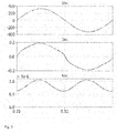
Fig. 3 zeigt den zeitlichen Verlauf der (noch nicht gleichgerichteten) Versorgungsspannung des Eingangsstromes sowie der zyklischen Veränderung der Ton-Zeit, und -
Figur 4 zeigt den Effekt der erfindungsgemäßen Ausgestaltung auf die relative Phasenlage zwischen dem Verlauf der Ton-Zeit und dem zeitlichen Verlauf der gleichgerichteten Versorgungspannung. - Die Erfindung geht von der Schaltung von
Figur 1 aus, so dass sämtliche Ausführungen zurFigur 1 auch bei der Erfindung Anwendung finden. - Die Erfindung bezieht sich also wie aus
Figur 2 ersichtlich darauf, dass gezielt und somit zusätzlich zu einer etwaigen intrinsisch vorliegenden negativen Phasenverschiebung die Phase der Ton-Zeit Variation im Wesentlichen übereinstimmend zu der Phase der gleichgerichteten Wechselspannung ergibt. Im Wesentlichen übereinstimmend bedeutet das, dass die Phase nicht mehr als +/- 30 Grad abweicht. - Die zusätzliche Phasenverschiebung kann fest vorgegeben sein, bspw. indem sie werksseitig vorgegeben wird.
- Alternativ kann sie adaptiv sein, bspw. abhängig von einer Erfassung der vorliegenden Gesamt-Phasenlage, um davon abhängig die zusätzliche Phasenverschiebung einzustellen.
- Die zusätzliche Phasenverschiebung kann die Frequenz oder allgemein den Verlauf der gleichgerichteten Versorgungsspannung berücksichtigen. Alternativ kann auch der LED-Strom bei Messung vor dem Kondensator herangezogen werden, da dieser die gleiche Phasenlage wie die gleichgerichtete Versorgungsspannung aufweist.
- Aufgrund der negativen Rückkopplung des Rückführsignales (siehe invertierender Eingang des Komparators 7 in
Figur 2 ) liegt bereits intrinsisch eine Phasenverschiebung von -180 Grad vor. Gemäß der Erfindung wird somit gezielt eine weitere negative Phasenverschiebung im Bereich von -140 Grad bis -180 Grad beaufschlagt, sodass sich annähernd eine Gesamtphasenverschiebung im Bereich von - 360 Grad ergibt, was somit zu der Koinzidenz führt, wie sie inFigur 4 dargestellt ist. Dort ist ersichtlich, dass die Täler und Spitzen der gleichgerichteten Wechselversorgungsspannung im Wesentlichen die gleiche zeitliche Lage aufweisen, wie die entsprechenden Spitzen bzw. Täler der Ton-Zeit Variation. - Diese gleichlaufende zeitliche Lage zwischen der Ton-Zeit Variation und der gleichgerichteten Versorgungspannung führt zu der erfindungsgemäßen Verbesserung des THD-Werts.
- Wie in
Figur 2 gezeigt, kann diese zusätzliche gezielte Phasenverschiebung durch eine Phasenverschiebungseinheit 9 erreicht werden, die an unterschiedlichen Orten der Regelschleife angeordnet werden kann. Mit dem Bezugszeichen 9A ist eine Phasenverschiebungseinheit angedeutet, die Rückführpfad des Istwert-Signals 5 wirksam ist. - Mit dem Bezugszeichen 9D ist eine Phasenverschiebungseinheit angedeutet, die in dem Steuersignalpfad 15 wirksam ist.
- Mit dem Bezugszeichen 9C ist eine Phasenverschiebungseinheit angedeutet, die durch Implementierung in dem Algorithmus des Controllers 4 selbst wirksam ist.
- Schließlich ist mit dem Bezugszeichen 9D eine Phasenverschiebungseinheit angedeutet, die in dem Bereich zwischen dem Sollwert/Istwert-Vergleich und dem Algorithmus des Controllers 4 wirksam ist.
- Ziel der Erfindung ist es also, dass eine effektive Phasenverschiebung zwischen dem gleichgerichteten Eingangsspannungssignal und dem Ton-Zeit Verlauf von etwa -360 Grad vorliegt.
- Im aufgeführten Ausführungsbeispiel von
Figur 2 erfolgt die Ausgangsstromerfassung 20 vor dem Ausgangskondensator 12, so dass der Diodenstrom gemessen wird. In diesem Fall ist die Phasenverschiebungseinheit 9 so auszugestalten, dass sie eine zusätzliche Phasenverschiebung von -180 Grad bewirkt, da in diesem Fall das gemessene Istwert-Signal die gleiche Phasenlage wie die gleichgerichtete Eingangsspannung aufweisen wird. - Grundsätzlich kann indessen auch tatsächlich der LED-Strom auch nach dem Ausgangskondensator 12 gemessen werden.
- Wie in
Figur 4 ersichtlich ist der LED-Strom Imeas-av mit dem Verlauf der gleichgerichteten Versorgungsspannung moduliert und weist auch die gleiche Phasenlage auf.
Claims (7)
- Konverter zur Versorgung einer LED-Last (1), aufweisend:- einen getakteten Konverter, insbesondere einen Buck-Boost-Konverter (2) mit einem Schalter (3),- wobei der Schalter (3) durch eine Regelschaltung (4) angesteuert wird, die ein Rückführsignal (5), insbesondere einen den Strom durch die LED-Last oder durch eine Diode wiedergebenden Wert, mit einem Sollwert (6) vergleicht (7), abhängig von dem Vergleichsergebnis eine Einschaltzeitdauer Ton für den Schalter (3) bestimmt und entsprechend den Schalter (3) ansteuert,
gekennzeichnet durch- eine Phasenverschiebungseinheit (9), die in dem Pfad vom Abgriff des Rückführsignals (5) zu dem Ansteuersignal des Schalters (3) vorgesehen ist. - Konverter nach Anspruch 1,
bei dem die Phasenverschiebungseinheit (9) eine resultierende Phasenverschiebung der zyklischen Veränderung der Ton-Zeit von -320 Grad bis -360 Grad zu dem Verlauf einer den Konverter (2) versorgenden gleichgerichteten Wechselspannung (8) bewirkt. - Konverter nach Anspruch 1 oder 2,
bei dem die Phasenverschiebungseinheit (9) in dem Rückführpfad und/oder nach dem Vergleich wirksam ist. - Konverter nach einem der vorhergehenden Ansprüche,
bei dem das Rückführsignal an einem Punkt abgegriffen ist, der zwischen dem Schalter und einem Kondensator liegt, welcher Kondensator die Leuchtmittelstrecke versorgt. - Konverter nach einem der vorhergehenden Ansprüche,
bei dem der Schalter fest-frequent oder mit variabler Frequenz betrieben wird. - Konverter nach einem der vorhergehenden Ansprüche,
bei dem die Ausschalt-Zeitdauer TOFF des Schalters fest oder variabel ist. - Konverter zur Versorgung einer LED-Last (1), aufweisend:einen getakteten Konverter, insbesondere einen Buck-Boost-Konverter (2) mit einem Schalter (3),wobei der Schalter (3) durch eine Regelschaltung (4) angesteuert wird, die ein Rückführsignal (5), insbesondere einen den Strom durch die LED-Last wiedergebenden Wert mit einem Sollwert (6) vergleicht, abhängig von dem Vergleichsergebnis eine Einschaltzeitdauer Ton für den Schalter (3) bestimmt und entsprechend den Schalter (3) ansteuert,gekennzeichnet durcheine resultierende Phasenverschiebung der zyklischen Veränderung der Ton-Zeit von -320 Grad bis -360 Grad zu dem Verlauf einer den Konverter (2) versorgenden gleichgerichteten Wechselspannung (8).
Applications Claiming Priority (1)
| Application Number | Priority Date | Filing Date | Title |
|---|---|---|---|
| DE202017102691.4U DE202017102691U1 (de) | 2017-05-05 | 2017-05-05 | Buck-Boost-Konverter mit verbessertem THD-Verhalten |
Publications (2)
| Publication Number | Publication Date |
|---|---|
| EP3399841A1 true EP3399841A1 (de) | 2018-11-07 |
| EP3399841B1 EP3399841B1 (de) | 2023-01-04 |
Family
ID=61972002
Family Applications (1)
| Application Number | Title | Priority Date | Filing Date |
|---|---|---|---|
| EP18166936.7A Active EP3399841B1 (de) | 2017-05-05 | 2018-04-12 | Buck-boost-konverter mit verbessertem thd-verhalten |
Country Status (3)
| Country | Link |
|---|---|
| EP (1) | EP3399841B1 (de) |
| AT (1) | AT17608U1 (de) |
| DE (1) | DE202017102691U1 (de) |
Citations (3)
| Publication number | Priority date | Publication date | Assignee | Title |
|---|---|---|---|---|
| WO2004100614A1 (en) * | 2003-05-07 | 2004-11-18 | Koninklijke Philips Electronics N.V. | Current control method and circuit for light emitting diodes |
| US7498786B2 (en) * | 2003-12-01 | 2009-03-03 | Fairchild Semiconductor Corporation | Digital control of switching voltage regulators |
| DE102013215966A1 (de) * | 2013-04-26 | 2014-10-30 | Tridonic Gmbh & Co Kg | Schaltungsanordnung und Verfahren zum Betreiben eines Leuchtmittels |
Family Cites Families (1)
| Publication number | Priority date | Publication date | Assignee | Title |
|---|---|---|---|---|
| US20120098869A1 (en) * | 2010-10-22 | 2012-04-26 | Himax Analogic, Inc. | Light Emitting Diode Circuit, Light Emitting Diode Driving Circuit, and Method for Driving Light Emitting Diode Channels |
-
2017
- 2017-05-05 DE DE202017102691.4U patent/DE202017102691U1/de not_active Expired - Lifetime
- 2017-09-08 AT ATGM194/2017U patent/AT17608U1/de not_active IP Right Cessation
-
2018
- 2018-04-12 EP EP18166936.7A patent/EP3399841B1/de active Active
Patent Citations (3)
| Publication number | Priority date | Publication date | Assignee | Title |
|---|---|---|---|---|
| WO2004100614A1 (en) * | 2003-05-07 | 2004-11-18 | Koninklijke Philips Electronics N.V. | Current control method and circuit for light emitting diodes |
| US7498786B2 (en) * | 2003-12-01 | 2009-03-03 | Fairchild Semiconductor Corporation | Digital control of switching voltage regulators |
| DE102013215966A1 (de) * | 2013-04-26 | 2014-10-30 | Tridonic Gmbh & Co Kg | Schaltungsanordnung und Verfahren zum Betreiben eines Leuchtmittels |
Non-Patent Citations (2)
| Title |
|---|
| KA-FAI CHAN ET AL: "Generalized Type III controller design interface for DC-DC converters", 2013 IEEE INTERNATIONAL CONFERENCE OF IEEE REGION 10 (TENCON 2013), IEEE, 1 November 2015 (2015-11-01), pages 1 - 6, XP032845164, ISSN: 2159-3442, ISBN: 978-1-4799-2825-5, [retrieved on 20160105], DOI: 10.1109/TENCON.2015.7373052 * |
| ROBERT SHEEHAN ET AL: "Switch-mode power converter compensation made easy", TEXAS INSTRUMENTS POWER SUPPLY DESIGN SEMINAR 2016/ 2017, 1 September 2016 (2016-09-01), pages 1 - 38, XP055486626, Retrieved from the Internet <URL:https://www.ti.com/seclit/ml/slup340/slup340.pdf> [retrieved on 20180621] * |
Also Published As
| Publication number | Publication date |
|---|---|
| AT17608U1 (de) | 2022-08-15 |
| EP3399841B1 (de) | 2023-01-04 |
| DE202017102691U1 (de) | 2018-08-07 |
Similar Documents
| Publication | Publication Date | Title |
|---|---|---|
| DE102004033354B4 (de) | Verfahren zur Ansteuerung eines Schalters in einem Hochsetzsteller und Ansteuerschaltung | |
| DE112018004109T5 (de) | Digitale steuerung eines verschachtelten leistungswandlers im geschalteten boundary-modus | |
| DE112018004065T5 (de) | Digitale steuerung eines leistungswandlers im switched boundary-modus ohne stromsensor | |
| DE112006002495T5 (de) | Digitale Steuereinrichtung zur Leistungsfaktorkorrektur und diese aufweisende Wechselspannungs-zu-Gleichspannungsversorgung | |
| EP3350911B1 (de) | Pfc-modul für lückenden betrieb | |
| DE112018004068T5 (de) | Digitale steuerung eines verschachtelten leistungswandlers im geschalteten boundary-modus mit verringerter übergangsverzerrung | |
| DE10327956A1 (de) | Schaltungsanordnung zur Spannungsversorgung einer Last | |
| DE112016001795T5 (de) | Leuchtdioden-treiberschaltung und leuchtdioden -beleuchtungsvorrichtung | |
| DE102013216155B4 (de) | Elektronisches Vorschaltgerät zum Betreiben mindestens einer ersten Kaskade von LEDs | |
| DE102016110422A1 (de) | Dimmbestromungsschaltung und leuchte | |
| EP2512207B1 (de) | Treiberschaltung und Verfahren zum Versorgen einer LED sowie Leuchtmittel | |
| DE102009017139A1 (de) | Leistungsregelung von LED | |
| DE102011088426A1 (de) | Elektronisches vorschaltgerät und verfahren zum betreiben mindestens einer ersten kaskade und einer zweiten kaskade von leds | |
| DE102012215933A1 (de) | Elektronisches Vorschaltgerät zum Betreiben mindestens einer ersten und einer zweiten Kaskade von LEDs | |
| DE202017102691U1 (de) | Buck-Boost-Konverter mit verbessertem THD-Verhalten | |
| DE112015002852T5 (de) | Beleuchtungseinrichtung | |
| DE102013216153A1 (de) | Elektronisches Vorschaltgerät zum Betreiben mindestens einer ersten und einer zweiten Kaskade von LEDs | |
| DE102014219787A1 (de) | Schaltnetzteil mit zumindest einem Leistungsteil und zumindest einem Hilfsnetzteil | |
| EP2713489A1 (de) | Verfahren für Niedriglastbetrieb eines aktiven PFC-Wandlers mittels Fenstermodulation mit gesteuerter Fensterbreite | |
| EP3711457B1 (de) | Betriebsschaltung für ein led-leuchtmittel | |
| DE19848428C2 (de) | Gestufter Spannungskonstanthalter | |
| EP3123602B1 (de) | Leistungsfaktorkorrekturschaltung (pfc) mit thd-korrektur | |
| AT17523U1 (de) | Schaltregler und Verfahren zum Betreiben von Leuchtmitteln mit Lichtschwankungs-Unterdrückung | |
| DE102008010398A1 (de) | Verfahren zur Ermittlung einer Ansteuerung einer elektrischen Energieversorgung | |
| DE102016210517A1 (de) | Verfahren zum Regeln einer Ausgangsleistung einer elektrischen Wechselspannung |
Legal Events
| Date | Code | Title | Description |
|---|---|---|---|
| PUAI | Public reference made under article 153(3) epc to a published international application that has entered the european phase |
Free format text: ORIGINAL CODE: 0009012 |
|
| STAA | Information on the status of an ep patent application or granted ep patent |
Free format text: STATUS: THE APPLICATION HAS BEEN PUBLISHED |
|
| AK | Designated contracting states |
Kind code of ref document: A1 Designated state(s): AL AT BE BG CH CY CZ DE DK EE ES FI FR GB GR HR HU IE IS IT LI LT LU LV MC MK MT NL NO PL PT RO RS SE SI SK SM TR |
|
| AX | Request for extension of the european patent |
Extension state: BA ME |
|
| STAA | Information on the status of an ep patent application or granted ep patent |
Free format text: STATUS: REQUEST FOR EXAMINATION WAS MADE |
|
| 17P | Request for examination filed |
Effective date: 20190328 |
|
| RBV | Designated contracting states (corrected) |
Designated state(s): AL AT BE BG CH CY CZ DE DK EE ES FI FR GB GR HR HU IE IS IT LI LT LU LV MC MK MT NL NO PL PT RO RS SE SI SK SM TR |
|
| STAA | Information on the status of an ep patent application or granted ep patent |
Free format text: STATUS: EXAMINATION IS IN PROGRESS |
|
| 17Q | First examination report despatched |
Effective date: 20210202 |
|
| REG | Reference to a national code |
Ref country code: DE Ref legal event code: R079 Ref document number: 502018011348 Country of ref document: DE Free format text: PREVIOUS MAIN CLASS: H05B0033080000 Ipc: H05B0045355000 |
|
| RIC1 | Information provided on ipc code assigned before grant |
Ipc: H05B 45/3725 20200101ALI20220620BHEP Ipc: H05B 45/355 20200101AFI20220620BHEP |
|
| GRAP | Despatch of communication of intention to grant a patent |
Free format text: ORIGINAL CODE: EPIDOSNIGR1 |
|
| STAA | Information on the status of an ep patent application or granted ep patent |
Free format text: STATUS: GRANT OF PATENT IS INTENDED |
|
| INTG | Intention to grant announced |
Effective date: 20221019 |
|
| GRAS | Grant fee paid |
Free format text: ORIGINAL CODE: EPIDOSNIGR3 |
|
| GRAA | (expected) grant |
Free format text: ORIGINAL CODE: 0009210 |
|
| STAA | Information on the status of an ep patent application or granted ep patent |
Free format text: STATUS: THE PATENT HAS BEEN GRANTED |
|
| AK | Designated contracting states |
Kind code of ref document: B1 Designated state(s): AL AT BE BG CH CY CZ DE DK EE ES FI FR GB GR HR HU IE IS IT LI LT LU LV MC MK MT NL NO PL PT RO RS SE SI SK SM TR |
|
| REG | Reference to a national code |
Ref country code: GB Ref legal event code: FG4D Free format text: NOT ENGLISH |
|
| REG | Reference to a national code |
Ref country code: DE Ref legal event code: R096 Ref document number: 502018011348 Country of ref document: DE |
|
| REG | Reference to a national code |
Ref country code: CH Ref legal event code: EP |
|
| REG | Reference to a national code |
Ref country code: AT Ref legal event code: REF Ref document number: 1542820 Country of ref document: AT Kind code of ref document: T Effective date: 20230115 |
|
| REG | Reference to a national code |
Ref country code: IE Ref legal event code: FG4D Free format text: LANGUAGE OF EP DOCUMENT: GERMAN |
|
| REG | Reference to a national code |
Ref country code: LT Ref legal event code: MG9D |
|
| REG | Reference to a national code |
Ref country code: NL Ref legal event code: MP Effective date: 20230104 |
|
| PG25 | Lapsed in a contracting state [announced via postgrant information from national office to epo] |
Ref country code: NL Free format text: LAPSE BECAUSE OF FAILURE TO SUBMIT A TRANSLATION OF THE DESCRIPTION OR TO PAY THE FEE WITHIN THE PRESCRIBED TIME-LIMIT Effective date: 20230104 |
|
| P01 | Opt-out of the competence of the unified patent court (upc) registered |
Effective date: 20230530 |
|
| PG25 | Lapsed in a contracting state [announced via postgrant information from national office to epo] |
Ref country code: RS Free format text: LAPSE BECAUSE OF FAILURE TO SUBMIT A TRANSLATION OF THE DESCRIPTION OR TO PAY THE FEE WITHIN THE PRESCRIBED TIME-LIMIT Effective date: 20230104 Ref country code: PT Free format text: LAPSE BECAUSE OF FAILURE TO SUBMIT A TRANSLATION OF THE DESCRIPTION OR TO PAY THE FEE WITHIN THE PRESCRIBED TIME-LIMIT Effective date: 20230504 Ref country code: NO Free format text: LAPSE BECAUSE OF FAILURE TO SUBMIT A TRANSLATION OF THE DESCRIPTION OR TO PAY THE FEE WITHIN THE PRESCRIBED TIME-LIMIT Effective date: 20230404 Ref country code: LV Free format text: LAPSE BECAUSE OF FAILURE TO SUBMIT A TRANSLATION OF THE DESCRIPTION OR TO PAY THE FEE WITHIN THE PRESCRIBED TIME-LIMIT Effective date: 20230104 Ref country code: LT Free format text: LAPSE BECAUSE OF FAILURE TO SUBMIT A TRANSLATION OF THE DESCRIPTION OR TO PAY THE FEE WITHIN THE PRESCRIBED TIME-LIMIT Effective date: 20230104 Ref country code: HR Free format text: LAPSE BECAUSE OF FAILURE TO SUBMIT A TRANSLATION OF THE DESCRIPTION OR TO PAY THE FEE WITHIN THE PRESCRIBED TIME-LIMIT Effective date: 20230104 Ref country code: ES Free format text: LAPSE BECAUSE OF FAILURE TO SUBMIT A TRANSLATION OF THE DESCRIPTION OR TO PAY THE FEE WITHIN THE PRESCRIBED TIME-LIMIT Effective date: 20230104 |
|
| PG25 | Lapsed in a contracting state [announced via postgrant information from national office to epo] |
Ref country code: SE Free format text: LAPSE BECAUSE OF FAILURE TO SUBMIT A TRANSLATION OF THE DESCRIPTION OR TO PAY THE FEE WITHIN THE PRESCRIBED TIME-LIMIT Effective date: 20230104 Ref country code: PL Free format text: LAPSE BECAUSE OF FAILURE TO SUBMIT A TRANSLATION OF THE DESCRIPTION OR TO PAY THE FEE WITHIN THE PRESCRIBED TIME-LIMIT Effective date: 20230104 Ref country code: IS Free format text: LAPSE BECAUSE OF FAILURE TO SUBMIT A TRANSLATION OF THE DESCRIPTION OR TO PAY THE FEE WITHIN THE PRESCRIBED TIME-LIMIT Effective date: 20230504 Ref country code: GR Free format text: LAPSE BECAUSE OF FAILURE TO SUBMIT A TRANSLATION OF THE DESCRIPTION OR TO PAY THE FEE WITHIN THE PRESCRIBED TIME-LIMIT Effective date: 20230405 Ref country code: FI Free format text: LAPSE BECAUSE OF FAILURE TO SUBMIT A TRANSLATION OF THE DESCRIPTION OR TO PAY THE FEE WITHIN THE PRESCRIBED TIME-LIMIT Effective date: 20230104 |
|
| REG | Reference to a national code |
Ref country code: DE Ref legal event code: R097 Ref document number: 502018011348 Country of ref document: DE |
|
| PG25 | Lapsed in a contracting state [announced via postgrant information from national office to epo] |
Ref country code: SM Free format text: LAPSE BECAUSE OF FAILURE TO SUBMIT A TRANSLATION OF THE DESCRIPTION OR TO PAY THE FEE WITHIN THE PRESCRIBED TIME-LIMIT Effective date: 20230104 Ref country code: RO Free format text: LAPSE BECAUSE OF FAILURE TO SUBMIT A TRANSLATION OF THE DESCRIPTION OR TO PAY THE FEE WITHIN THE PRESCRIBED TIME-LIMIT Effective date: 20230104 Ref country code: EE Free format text: LAPSE BECAUSE OF FAILURE TO SUBMIT A TRANSLATION OF THE DESCRIPTION OR TO PAY THE FEE WITHIN THE PRESCRIBED TIME-LIMIT Effective date: 20230104 Ref country code: DK Free format text: LAPSE BECAUSE OF FAILURE TO SUBMIT A TRANSLATION OF THE DESCRIPTION OR TO PAY THE FEE WITHIN THE PRESCRIBED TIME-LIMIT Effective date: 20230104 Ref country code: CZ Free format text: LAPSE BECAUSE OF FAILURE TO SUBMIT A TRANSLATION OF THE DESCRIPTION OR TO PAY THE FEE WITHIN THE PRESCRIBED TIME-LIMIT Effective date: 20230104 |
|
| PLBE | No opposition filed within time limit |
Free format text: ORIGINAL CODE: 0009261 |
|
| STAA | Information on the status of an ep patent application or granted ep patent |
Free format text: STATUS: NO OPPOSITION FILED WITHIN TIME LIMIT |
|
| PG25 | Lapsed in a contracting state [announced via postgrant information from national office to epo] |
Ref country code: SK Free format text: LAPSE BECAUSE OF FAILURE TO SUBMIT A TRANSLATION OF THE DESCRIPTION OR TO PAY THE FEE WITHIN THE PRESCRIBED TIME-LIMIT Effective date: 20230104 |
|
| REG | Reference to a national code |
Ref country code: CH Ref legal event code: PL |
|
| 26N | No opposition filed |
Effective date: 20231005 |
|
| PG25 | Lapsed in a contracting state [announced via postgrant information from national office to epo] |
Ref country code: LU Free format text: LAPSE BECAUSE OF NON-PAYMENT OF DUE FEES Effective date: 20230412 |
|
| REG | Reference to a national code |
Ref country code: BE Ref legal event code: MM Effective date: 20230430 |
|
| PG25 | Lapsed in a contracting state [announced via postgrant information from national office to epo] |
Ref country code: MC Free format text: LAPSE BECAUSE OF FAILURE TO SUBMIT A TRANSLATION OF THE DESCRIPTION OR TO PAY THE FEE WITHIN THE PRESCRIBED TIME-LIMIT Effective date: 20230104 |
|
| PG25 | Lapsed in a contracting state [announced via postgrant information from national office to epo] |
Ref country code: SI Free format text: LAPSE BECAUSE OF FAILURE TO SUBMIT A TRANSLATION OF THE DESCRIPTION OR TO PAY THE FEE WITHIN THE PRESCRIBED TIME-LIMIT Effective date: 20230104 Ref country code: MC Free format text: LAPSE BECAUSE OF FAILURE TO SUBMIT A TRANSLATION OF THE DESCRIPTION OR TO PAY THE FEE WITHIN THE PRESCRIBED TIME-LIMIT Effective date: 20230104 Ref country code: LI Free format text: LAPSE BECAUSE OF NON-PAYMENT OF DUE FEES Effective date: 20230430 Ref country code: CH Free format text: LAPSE BECAUSE OF NON-PAYMENT OF DUE FEES Effective date: 20230430 |
|
| REG | Reference to a national code |
Ref country code: IE Ref legal event code: MM4A |
|
| REG | Reference to a national code |
Ref country code: DE Ref legal event code: R084 Ref document number: 502018011348 Country of ref document: DE |
|
| PG25 | Lapsed in a contracting state [announced via postgrant information from national office to epo] |
Ref country code: BE Free format text: LAPSE BECAUSE OF NON-PAYMENT OF DUE FEES Effective date: 20230430 |
|
| PG25 | Lapsed in a contracting state [announced via postgrant information from national office to epo] |
Ref country code: IE Free format text: LAPSE BECAUSE OF NON-PAYMENT OF DUE FEES Effective date: 20230412 |
|
| PG25 | Lapsed in a contracting state [announced via postgrant information from national office to epo] |
Ref country code: IE Free format text: LAPSE BECAUSE OF NON-PAYMENT OF DUE FEES Effective date: 20230412 |
|
| PG25 | Lapsed in a contracting state [announced via postgrant information from national office to epo] |
Ref country code: IT Free format text: LAPSE BECAUSE OF FAILURE TO SUBMIT A TRANSLATION OF THE DESCRIPTION OR TO PAY THE FEE WITHIN THE PRESCRIBED TIME-LIMIT Effective date: 20230104 |
|
| REG | Reference to a national code |
Ref country code: AT Ref legal event code: MM01 Ref document number: 1542820 Country of ref document: AT Kind code of ref document: T Effective date: 20230412 |
|
| PG25 | Lapsed in a contracting state [announced via postgrant information from national office to epo] |
Ref country code: AT Free format text: LAPSE BECAUSE OF NON-PAYMENT OF DUE FEES Effective date: 20230412 |
|
| PG25 | Lapsed in a contracting state [announced via postgrant information from national office to epo] |
Ref country code: AT Free format text: LAPSE BECAUSE OF NON-PAYMENT OF DUE FEES Effective date: 20230412 |
|
| PG25 | Lapsed in a contracting state [announced via postgrant information from national office to epo] |
Ref country code: BG Free format text: LAPSE BECAUSE OF FAILURE TO SUBMIT A TRANSLATION OF THE DESCRIPTION OR TO PAY THE FEE WITHIN THE PRESCRIBED TIME-LIMIT Effective date: 20230104 |
|
| PG25 | Lapsed in a contracting state [announced via postgrant information from national office to epo] |
Ref country code: BG Free format text: LAPSE BECAUSE OF FAILURE TO SUBMIT A TRANSLATION OF THE DESCRIPTION OR TO PAY THE FEE WITHIN THE PRESCRIBED TIME-LIMIT Effective date: 20230104 |
|
| PGFP | Annual fee paid to national office [announced via postgrant information from national office to epo] |
Ref country code: DE Payment date: 20250428 Year of fee payment: 8 |
|
| PGFP | Annual fee paid to national office [announced via postgrant information from national office to epo] |
Ref country code: GB Payment date: 20250422 Year of fee payment: 8 |
|
| PGFP | Annual fee paid to national office [announced via postgrant information from national office to epo] |
Ref country code: FR Payment date: 20250424 Year of fee payment: 8 |
|
| PG25 | Lapsed in a contracting state [announced via postgrant information from national office to epo] |
Ref country code: CY Free format text: LAPSE BECAUSE OF FAILURE TO SUBMIT A TRANSLATION OF THE DESCRIPTION OR TO PAY THE FEE WITHIN THE PRESCRIBED TIME-LIMIT; INVALID AB INITIO Effective date: 20180412 |
|
| PG25 | Lapsed in a contracting state [announced via postgrant information from national office to epo] |
Ref country code: HU Free format text: LAPSE BECAUSE OF FAILURE TO SUBMIT A TRANSLATION OF THE DESCRIPTION OR TO PAY THE FEE WITHIN THE PRESCRIBED TIME-LIMIT; INVALID AB INITIO Effective date: 20180412 |
|
| PG25 | Lapsed in a contracting state [announced via postgrant information from national office to epo] |
Ref country code: TR Free format text: LAPSE BECAUSE OF FAILURE TO SUBMIT A TRANSLATION OF THE DESCRIPTION OR TO PAY THE FEE WITHIN THE PRESCRIBED TIME-LIMIT Effective date: 20230104 |