EP3399393A1 - Input device - Google Patents
Input device Download PDFInfo
- Publication number
- EP3399393A1 EP3399393A1 EP16881546.2A EP16881546A EP3399393A1 EP 3399393 A1 EP3399393 A1 EP 3399393A1 EP 16881546 A EP16881546 A EP 16881546A EP 3399393 A1 EP3399393 A1 EP 3399393A1
- Authority
- EP
- European Patent Office
- Prior art keywords
- input device
- transparent
- wiring units
- area
- metal wiring
- Prior art date
- Legal status (The legal status is an assumption and is not a legal conclusion. Google has not performed a legal analysis and makes no representation as to the accuracy of the status listed.)
- Granted
Links
Images





Classifications
-
- G—PHYSICS
- G06—COMPUTING OR CALCULATING; COUNTING
- G06F—ELECTRIC DIGITAL DATA PROCESSING
- G06F3/00—Input arrangements for transferring data to be processed into a form capable of being handled by the computer; Output arrangements for transferring data from processing unit to output unit, e.g. interface arrangements
- G06F3/01—Input arrangements or combined input and output arrangements for interaction between user and computer
- G06F3/03—Arrangements for converting the position or the displacement of a member into a coded form
- G06F3/041—Digitisers, e.g. for touch screens or touch pads, characterised by the transducing means
- G06F3/0416—Control or interface arrangements specially adapted for digitisers
- G06F3/04164—Connections between sensors and controllers, e.g. routing lines between electrodes and connection pads
-
- G—PHYSICS
- G06—COMPUTING OR CALCULATING; COUNTING
- G06F—ELECTRIC DIGITAL DATA PROCESSING
- G06F3/00—Input arrangements for transferring data to be processed into a form capable of being handled by the computer; Output arrangements for transferring data from processing unit to output unit, e.g. interface arrangements
- G06F3/01—Input arrangements or combined input and output arrangements for interaction between user and computer
- G06F3/03—Arrangements for converting the position or the displacement of a member into a coded form
- G06F3/041—Digitisers, e.g. for touch screens or touch pads, characterised by the transducing means
- G06F3/0412—Digitisers structurally integrated in a display
-
- G—PHYSICS
- G06—COMPUTING OR CALCULATING; COUNTING
- G06F—ELECTRIC DIGITAL DATA PROCESSING
- G06F3/00—Input arrangements for transferring data to be processed into a form capable of being handled by the computer; Output arrangements for transferring data from processing unit to output unit, e.g. interface arrangements
- G06F3/01—Input arrangements or combined input and output arrangements for interaction between user and computer
- G06F3/03—Arrangements for converting the position or the displacement of a member into a coded form
- G06F3/041—Digitisers, e.g. for touch screens or touch pads, characterised by the transducing means
- G06F3/044—Digitisers, e.g. for touch screens or touch pads, characterised by the transducing means by capacitive means
Definitions
- the present invention relates to an input device that includes transparent electrodes and a decorative area, and, in particular, relates to an input device that includes a wiring unit in the decorative area.
- Touch panel type input devices are popular and mainly used as a mobile device.
- an operation input is detected according to a contact of an operation body on an operation surface of the mobile device, or according to a change of capacitance when the operation body comes close to the operation surface.
- an input device 900 described in Patent Document 1 is known. In the following, referring to Fig. 12 and Fig. 13 , the input device 900 will be described.
- the input device 900 includes an input area 911 on a lower transparent substrate 932 of a lower substrate 922, and the input area 911 is surrounded by a frame-shaped decorative area 912.
- the "decorative area” refers to an area used for preventing an area of the lower substrate 922 illustrated in Fig. 12 from being seen from the operation surface side of the touch panel.
- the decorative area 912 is an area decorated (black-painted) by a decorative layer 934 included in the decorative area 912. Further, practically, the decorative area 912 is a "non-input area” that is an area not used as an operation surface.
- the input device 900 includes transparent electrodes 914 and wiring units 915 (915a-915j) that are electrically connected to the transparent electrodes 914.
- the wiring units 915 have a layer structure including a first wiring layer 916 and a second wiring layer 925 (925f-925h).
- the first wiring layer 916 is a transparent conductive layer that is integrated with the transparent electrodes 914 that are formed on the surface of the transparent substrate.
- the second wiring layer 925 is formed by a metal layer.
- the transparent electrodes 914 are included in the input area 911, and the second wiring layer 925 is included in the decorative area 912 that is located outside the input area 911. Further, the first wiring layer 916 is provided extending into both the input area 911 and the decorative area 912.
- the input device 900 provides an effect of reducing the electric resistance of the wiring unit by forming the second wiring layer 925 as a metal wiring unit on the first wiring layer 916 as a transparent wiring unit.
- Patent Document 1 Japanese Unexamined Patent Application Publication No. 2012-043298
- the metal wiring unit cannot be seen due to the decorative layer included in the decorative area when the operation surface side of the touch panel is viewed from a direction orthogonal to the transparent substrate, the metal wiring unit can be seen when viewed from a direction oblique to the transparent substrate.
- the touch panel is mounted on the center console of a vehicle.
- a driver and a passenger in the passenger seat who are main operators of the touch panel, look at the operation surface always from a direction oblique to the transparent substrate, and thus, the metal wiring unit included in the decorative area can be seen by the operators.
- An object of the present invention is to provide an input device in which the metal wiring unit cannot be readily seen from the operation surface side.
- the input device includes: a transparent substrate with a display area and a decorative area; transparent electrodes that are provided in the display area on a side opposite to an operation surface; a decorative layer that is provided in the decorative area; and a wiring unit that is provided on a side opposite to a surface member with respect to the decorative layer, the surface member including the operation surface.
- the wiring unit has a layered structure in which metal wiring units and transparent wiring units are layered, the transparent wiring units being a transparent conductive layer integrally formed with the transparent electrodes.
- the transparent wiring units include transparent connection wiring units that extend into both the display area and the decorative area to connect the transparent electrodes electrically with the metal wiring units.
- a plurality of level parts are provided in the decorative area on the display area side with respect to the metal wiring units. The plurality of the level parts are provided to create gaps in a direction in which the metal wiring units extend in a plan view.
- the transparent connection wiring units extend from the display area to the decorative area through the gaps.
- the input device as described above includes the level parts that are provided on the display area side with respect to the metal wiring unit. As a result, even when the operation surface of the input device is viewed from a direction oblique to the transparent substrate, the incident light traveling towards the metal wiring unit is refracted by the level parts, and thus, it is possible to reduce the light amount incident on the metal wiring unit. Therefore, it is possible to prevent the metal wiring unit from being readily seen from the operation surface side.
- the input device described above is characterized by the level parts being protrusions provided on a side opposite to the operation surface.
- the incident light traveling towards the metal wiring unit is refracted by the protrusions provided on the side opposite to the operation surface. As a result, it is possible to prevent the light from being readily emitted onto the metal wiring unit.
- the input device described above is characterized by the plurality of the transparent connection wiring units extending from the display area to the decorative area through the gap in common.
- the number of the gaps it is possible to cause the number of the gaps to be less than the number of the wiring units by having a single gap shared by a plurality of the transparent connection wiring units. Therefore, it is possible to further prevent the metal wiring unit from being readily seen from the operation surface side.
- connection points between the transparent connection wiring units and the metal wiring unit in the decorative area being provided at positions that face the level parts.
- connection points between the transparent connection wiring units and the metal wiring unit are provided at positions avoiding the gaps, and thus, the action of the level parts for refracting the light can be further strengthened.
- the input device described above is characterized by a light shielding layer being provided on the display area side surface of the level part.
- the input device described above it is possible to cause the light traveling towards the metal wiring unit to be reflected by the light shielding layer, and thus, it is possible to reduce the amount of the light that is emitted onto the metal wiring unit.
- the input device described above is characterized by the level parts being recesses provided in the transparent substrate.
- the recesses provided in the transparent substrate refract the light that travels towards the metal wiring unit through the transparent substrate. As a result, it is possible to reduce the amount of the light that is emitted onto the metal wiring unit.
- the level parts are provided on the display area side with respect to the metal wiring unit. As a result, it is possible to cause the light traveling towards the metal wiring unit to be refracted by the level parts, and it is possible to prevent the light from being readily emitted onto the metal wiring unit. Therefore, it is possible to prevent the metal wiring unit from being readily seen from the operation surface side.
- the input device according to an embodiment of the present invention is an input device, installed in the center console of a vehicle, or the like, used for operating, for example, a car-navigation device, an air conditioner, a device related to drive operations, etc., and is an input device in which a capacitance type touch panel is used.
- the use of the input device according to an embodiment of the present invention is not limited to the above, and various modifications may be made.
- the X1 side of each drawing is referred to as a "right side”
- the X2 side is referred to as a "left side”
- the Y1 side is referred to as a “back side”
- the Y2 side is referred to as a "front side”
- the Z1 side is referred to as an "upper side”
- the Z2 side is referred to as a "lower side”.
- Fig. 1 is a plan view illustrating the input device 100 according to the first embodiment
- Fig. 2 is a sectional view of the input device 100 according to the first embodiment
- Fig. 2(a) is a sectional view viewed from an A-A line illustrated in Fig. 1 towards the right direction
- Fig. 2(b) is a sectional view viewed from a B-B line illustrated in Fig. 1 towards the back direction
- Fig. 3 is an enlarged sectional view of a part of the input device 100 according to the first embodiment, viewed from the B-B line illustrated in Fig.
- the input device 100 includes: the transparent substrate 30 including a display area 20 and a decorative area 10 on the surface; transparent electrodes 21 included in the display area 20; and a wiring unit 11 included in the decorative area 10.
- the transparent substrate 30 is formed in substantially a rectangular shape by a film-shaped transparent substrate made of polyethylene terephthalate (PET), or the like, with transparency, a glass substrate, etc.
- PET polyethylene terephthalate
- the display area 20 is an input area in the input device 100.
- a plurality of the transparent electrodes 21 are formed on the surface of the display area 20.
- the transparent electrodes 21 are an electrode pattern formed by causing transparent conductive material such as ITO (Indium Tin Oxide) to be directly applied to the surface of the transparent substrate 30 according to the vapor deposition, and by causing the transparent conductive material to be etched. Therefore, the display area 20 has transparency with respect to an up-and-down direction (thickness direction).
- the transparent electrodes 21 are directly formed on the surface of the transparent substrate 30, and the transparent electrodes 21 may be formed by causing a film-shaped substrate, on which transparent conductive material such as ITO has already been applied according to the vapor deposition and the electrodes have already been formed, to be attached to the surface of the transparent substrate 30 via a transparent adhesive.
- An operation surface for operating the input device 100 is provided on the upper side of the display area 20.
- the decorative area 10 is a frame-shaped area surrounding the display area 20 on the transparent substrate 30.
- the wiring unit 11 is formed in the decorative area 10.
- the decorative area 10 is an area used for preventing the wiring unit 11 included in the decorative area 10 from being seen from the operation surface 25 side of the touch panel installed in the center console of a vehicle, or the like.
- the decorative area 10 is a non-input area that is practically not used for input.
- the wiring unit 11, which is formed in the decorative area 10, includes a transparent conductive layer of a plurality of transparent wiring units 13, and includes a plurality of metal wiring units 12 corresponding to the transparent wiring units 13.
- the transparent wiring units 13 extend from the transparent electrodes 21 on the display area 20, and are formed integrally with the transparent electrodes 21.
- the transparent wiring units 13 includes transparent connection wiring units 13a, via which the transparent electrodes 21 on the display area 20 and the metal wiring units 12 are electrically connected.
- the transparent wiring units 13 also includes transparent lower-side wiring units 13b that are provided on the lower side of the metal wiring units 12.
- the metal wiring units 12 are layered on the transparent lower-side wiring units 13b that are located along the right side and the left side of the rectangular-shaped transparent substrate 30 as illustrated in Fig. 3 .
- the transparent wiring units 13 are formed extending from the transparent electrodes 21.
- the transparent wiring units 13 are made of transparent conductive material such as ITO.
- the metal wiring units 12 are made of metal material, such as Cu, Cu alloy, CuNi alloy, Ni, Ag, etc., whose electrical resistance value is less than the electrical resistance value of the transparent conductive material used for the transparent wiring units 13. It is possible to maintain low electrical resistance of the wiring unit 11 by forming the above-described metal wiring units 12 on the upper side of the transparent lower-side wiring units 13b.
- the surface member 33 including the operation surface 25 in the center is connected above the transparent electrodes 21 and the wiring unit 11 via an adhesive layer such as a double-sided adhesive tape (not shown).
- the material of the surface member 33 is not limited to a particular material.
- the surface member 33 is made of glass, transparent plastic, etc. Further, the adhesive layer is also made of a transparent material.
- a capacitance type input device like the input device 100, when a finger touches or comes close to the operation surface 25 above the transparent electrodes 21 included in the display area 20 illustrated in Fig. 2(b) , the capacitance between the finger and the transparent electrodes 21 is added to the capacitance between the transparent electrodes 21 and the ground, and the total capacitance is changed. Further, it is possible to calculate the contact point of the finger based on the change of the capacitance, and thus, it is determined that an input has been made.
- a frame-shaped decorative layer 35 is provided in the decorative area 10 of the transparent substrate 30 in accordance with the shape of the decorative area 10.
- the decorative layer 35 is formed between the decorative area 10 side of the surface member 33 and the wiring unit 11.
- the decorative layer 35 is formed by painting black the lower surface of the surface member 33.
- a plurality of level parts 15 are provided in the decorative area 10 on the display area 20 side with respect to the metal wiring units 12.
- the level parts 15 are formed in a direction from the front side to the back side (Y1-Y2 direction). Gaps 17 are provided between the adjacent level parts 15. Therefore, the level parts 15 are provided being separated from each other. In other words, the level parts 15 are provided in a direction, in which the metal wiring units 12 extend in a plan view, so as to create the gaps 17 between the adjacent level parts 15. Further, the above-described transparent connection units 13a extend from the display area 20 to the decorative area 10 through the gaps 17.
- the level parts 15 provided in the decorative area 10 are protrusions 15a provided on the transparent substrate 30 as illustrated in Fig. 2(a), Fig. 2(b) , and Fig. 3 .
- the protrusions 15a are molded together with the transparent substrate 30. Therefore, as is the case with the transparent substrate 30, the protrusions 15a are formed by a film-shaped transparent substrate made of polyethylene terephthalate, etc., with transparency, or by a glass substrate.
- the height of the level parts 15a is set higher than the height of the metal wiring units 12 that are layered on the transparent wiring units 13.
- a light beam L1 which travels towards the metal wiring units 12 from the operation surface 25 side, before hitting the metal wiring units 12, hits the display area 20 side of the level parts 15 as the protrusions 15a that are made of a transparent substrate.
- the light beam L1 is refracted due to the fact that the refractive index of the protrusions 15a made of a transparent substrate, a glass substrate, or the like, is greater than the refractive index of the air. Therefore, the light beam L1 does not travel towards the metal wiring units 12, and thus, it is possible to prevent the light beam L1 from readily hitting the metal wiring units 12. As a result, it is possible to prevent the metal wiring units 12 from being readily seen from the operation surface 25 side of the input device 100.
- FIG. 4 is a plan view illustrating the input device 110 according to the first modified example.
- Fig. 5 is an enlarged plan view illustrating the input device 120 according to the second modified example.
- Fig. 6 is an enlarged plan view illustrating the input device 130 according to the third modified example.
- the difference between the input device 100 according to the first embodiment and the input device 110 according to the first modified example exists in: the manners in which the transparent connection wiring units 13a are arranged; the lengths of the level parts 15; the widths of the gaps 17; the numbers of the level parts 15; and the numbers of the gaps 17, due to the difference in the arrangement manners. Further, the difference between the input device 100 and the input device 120 according to the second modified example exists only in the shapes of the transparent connection wiring units 13a. Further, the input device 130 according to the third modified example is obtained by combining the input device 110 according to the first modified example and the input device 120 according to the second modified example.
- connection points 14 are newly referred to as "connection points 14".
- the number of the level parts 15 located on the back left side is two, and the length of the level parts 15 is longer than that in the input device 100.
- the width of the gap 17 between the two level parts 15 is wider than that in the input device 100, and the wider gap 17 is referred to as a "wider gap 17a".
- two transparent connection wiring units 13a formed in the decorative area 10 extend through the wider gap 17a.
- the transparent wiring units 13 are arranged in such a way that multiple transparent connection wiring units 13a extend from the display area 20 to the decorative area 10 through a common gap 17 (that is, the wider gap 17a).
- the above-described arrangement of the transparent wiring units 13 is provided at a position in each of the back left side and the front right side.
- the above-described arrangement of the transparent wiring units 13 may be provided at a plurality of positions in each of the back left side and the front right side according to the number of transparent wiring units 13.
- the transparent connection wiring units 13a which extend from the display area 20 to the decorative area 10, are formed by extending and turning to the corresponding level part 15 side (Y1 direction) after extending through the gap 17. Further, the connection points 14, at which the metal wiring units 12 and the transparent connection wiring units 13a are connected, are provided in the vicinity of the level parts 15.
- connection points 14 between the transparent connection wiring units 13a and the metal wiring units 12 in the decorative area 10 are provided at positions that face the level parts 15.
- the connection points 14 are provided at two positions on the back left side of the input device 120.
- the connection points 14 may be provided at other positions such as on the right side of the input device 120.
- the width of the gap 17, which is located between the two level parts 15 on the back left side, is caused to be longer, and the longer gap 17 is referred to as a wider gap 17a.
- Two transparent connection wiring units 13a, which are formed in the decorative area 10, extend through the wider gap 17a.
- the transparent connection wiring units 13a, which extend from the display area 20 to the decorative area 10 are formed by extending and turning to a direction of the level part 15 that is on the front side (Y2 direction) after extending through the gap 17.
- the connection points 14 between the metal wiring units 12 and the transparent connection wiring units 13a are provided in the vicinity of the level parts 15.
- the transparent wiring units 13 are arranged in such a way that multiple transparent connection wiring units 13a extend from the display area 20 to the decorative area 10 through a common gap 17 (that is, the wider gap 17a), but also the connection points 14 between the transparent connection wiring units 13a and the metal wiring units 12 in the decorative area 10 are provided at positions that face the level parts 15.
- FIG. 7 is a plan view illustrating the input device 140 according to the fourth modified example
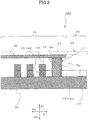
- Fig. 8 is an enlarged sectional view of the input device 150 according to the fifth modified example.
- the difference between the input device 100 according to the first embodiment and the input device 140 according to the fourth modified example exists only in the arrangements of the plurality of the level parts 15. Further, the difference between the input device 100 according to the first embodiment and the input device 150 according to the fifth modified example exists only in the structures of the level parts 15. Therefore, descriptions related to other than the above differences will be omitted. Further, the numerical code given to each part is the same as in the input device 100 according to the first embodiment.
- the positions of the plurality of the level parts 15 located on the back left side are shifted in a direction towards the left side of the transparent substrate 30 that has substantially a rectangular shape and the positions of the plurality of the level parts 15 located on the back right side are shifted in a direction towards the right side of the transparent substrate 30.
- the positions of the plurality of the level parts 15 are arranged not along the Y1-Y2 direction. In other words, in the input device 100, it is not necessary for the positions of the plurality of the level parts 15 to be arranged along the Y1-Y2 direction.
- a light shielding layer 15c is provided on the right side surface of a protrusion 15a, which is the level part 15 provided in the decorative area 10, (that is, the light shielding layer 15c is provided on the display area 20 side surface of the protrusion 15a).
- the light shielding layer 15c is formed by painting black the right side surface of the protrusion 15a made of a transparent substrate. It should be noted that the light shielding layer 15c may be formed, not by painting black the right side surface of the protrusion 15a, but by applying a satin-like finish to the side surface of the protrusion 15a.
- the light beam L1 traveling towards the metal wiring units 12 illustrated in Fig.8 hits the light shielding layer 15c on the display area 20 side surface of the protrusion 15a first, and then the light beam L1 is reflected by the light shielding layer 15c towards the display area 20 side. Therefore, it becomes possible to prevent the light beam L1 traveling towards the metal wiring units 12 from readily hitting the metal wiring units 12. As a result, it is possible to prevent the metal wiring units 12 from being readily seen from the operation surface 25 side of the input device 150.
- the light beam L1 is irregularly reflected by the light shielding layer 15c in the case where the light shielding layer 15c is formed by applying a satin-like finish to the side surface of the protrusion 15a. In this case, it is possible to prevent the light beam L1 from readily hitting the metal wiring units 12.
- Fig. 9 is a plan view illustrating the input device 200
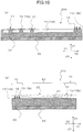
- Fig. 10 is a sectional view of the input device 200.
- Fig. 10(a) is a sectional view viewed from a C-C line illustrated in Fig. 9 towards the right direction
- Fig. 10(b) is a sectional view viewed from a D-D line illustrated in Fig. 9 towards the back direction
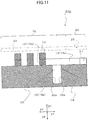
- Fig. 11 is an enlarged sectional view of a part of the input device 200 viewed from the D-D line illustrated in Fig. 9 towards the back direction.
- the difference between the input device 100 according to the first embodiment and the input device 200 according to the second embodiment exists only in the structures of the level parts 15. Therefore, descriptions related to other than the level parts 15 will be omitted. Further, the numerical code given to each part is the same as in the input device 100 according to the first embodiment.
- the input device 200 includes: a transparent substrate 30 including a display area 20 and a decorative area 10 on the surface; transparent electrodes 21 included in the display area 20; and a wiring unit 11 included in the decorative area 10.
- a plurality of level parts 15 are provided in the decorative area 10 on the display area 20 side with respect to the metal wiring units 12.
- the level parts 15 are formed in a direction from the front side to the back side (Y1-Y2 direction). Gaps 17 are provided between the adjacent level parts 15. Therefore, the level parts 15 are separated from each other. In other words, the level parts 15 are provided in a direction in which the metal wiring units 12 extend in a plan view so as to create gaps 17 between the adjacent level parts 15. Further, the above-described transparent connection units 13a extend from the display area 20 to the decorative area 10 through the gaps 17.
- the level parts 15 provided in the decorative area 10 are recesses 15b provided in the transparent substrate 30 as illustrated in Fig. 10(a), Fig. 10(b) , and Fig. 11 . Therefore, the level parts 15 are spaces, in which the substrate does not exist, formed together with the transparent substrate 30.
- the input device 200 by providing the level parts 15, which are recesses 15b, in the decorative area 10 on the display area 20 side with respect to the metal wiring units 12, it is possible to prevent the metal wiring units 12 from being readily seen from the operation surface 25 side of the input device 200.
- the light beam traveling towards the metal wiring units 12 includes, as illustrated in Fig. 11 , a light beam L2 that travels through the inside of the transparent substrate 30 that is formed by a film-shaped transparent substrate made of polyethylene terephthalate, etc., with transparency, or by a glass substrate.
- the light beam L2 which has traveled through the inside of the transparent substrate 30 illustrated in Fig. 11 and which is traveling towards the metal wiring units 12, reaches one of side walls 30a that serves as a boundary between the transparent substrate 30 and the recesses 15b on its way to the metal wiring units 12, and then enters the space of the recess 15b.
- the light beam L2 is refracted because of the fact that the refractive index of the air in the recess 15b is less than the refractive index of the transparent substrate 30.
- the light beam L2 when hitting the other of the side walls 30a from the recess 15b, the light beam L2 is also refracted because of the fact that the refractive index of the transparent substrate 30 is greater than the refractive index of the air in the recess 15b. Therefore, the light beam L2 will not readily hit the metal wiring units 12. As a result, it is possible to prevent the metal wiring units 12 from being readily seen from the operation surface 25 side of the input device 100.
- the level parts 15 are provided on the display area 20 side with respect to the metal wiring units 12. As a result, it is possible to cause the light beam L1 traveling towards the metal wiring units 12 to be refracted by the level parts 15, and it is possible to prevent the light beam L1 from readily hitting the metal wiring units 12. Therefore, it is possible to prevent the metal wiring units 12 from being readily seen from the operation surface 25 side.
- the light beam L1 traveling above the transparent substrate 30 towards the metal wiring units 12 is refracted by the protrusions 15a provided on the transparent substrate 30. As a result, it is possible to prevent the light beam L1 from readily hitting the metal wiring unit.
- connection points 14 between the transparent connection wiring units 13a and the metal wiring units 12 are provided at positions avoiding the gaps 17, and thus, the action of the level parts 15 for refracting the light beam L1 can be further strengthened.
- the light beam L2 traveling through the transparent substrate 30 towards the metal wiring units 12 is refracted by the recesses 15b provided in the transparent substrate 30. As a result, it is possible to reduce the amount of the light beam L2 that is emitted onto the metal wiring units 12.
- the level parts are provided on the display area side with respect to the metal wiring units. As a result, it is possible to cause the light beam traveling towards the metal wiring units to be refracted by the level parts, and it is possible to prevent the light beam from being readily emitted onto the metal wiring units. Therefore, it is possible to prevent the metal wiring units from being readily seen from the operation surface side.
- an embodiment of the present invention is not limited to the above-described embodiments. Various modifications may be possible without departing from the subject matter of the present invention.
- the input devices 110 through 150 are described as modified examples of the input device 100 according to the first embodiment.
- the input devices 110 through 150 may be described as modified examples of the input device 200 according to the second embodiment.
Landscapes
- Engineering & Computer Science (AREA)
- General Engineering & Computer Science (AREA)
- Theoretical Computer Science (AREA)
- Human Computer Interaction (AREA)
- Physics & Mathematics (AREA)
- General Physics & Mathematics (AREA)
- Computer Networks & Wireless Communication (AREA)
- Position Input By Displaying (AREA)
Abstract
Description
- The present invention relates to an input device that includes transparent electrodes and a decorative area, and, in particular, relates to an input device that includes a wiring unit in the decorative area.
- In recent years, a touch panel type input device has been developed as the input device. Touch panel type input devices are popular and mainly used as a mobile device. In the touch panel type input devices, an operation input is detected according to a contact of an operation body on an operation surface of the mobile device, or according to a change of capacitance when the operation body comes close to the operation surface.
- As one of the touch panel type input devices, an
input device 900 described in Patent Document 1 is known. In the following, referring toFig. 12 andFig. 13 , theinput device 900 will be described. - As illustrated in
Fig. 12 , theinput device 900 includes aninput area 911 on a lowertransparent substrate 932 of alower substrate 922, and theinput area 911 is surrounded by a frame-shapeddecorative area 912. Here, the "decorative area" refers to an area used for preventing an area of thelower substrate 922 illustrated inFig. 12 from being seen from the operation surface side of the touch panel. Thedecorative area 912 is an area decorated (black-painted) by a decorative layer 934 included in thedecorative area 912. Further, practically, thedecorative area 912 is a "non-input area" that is an area not used as an operation surface. - As illustrated in
Fig. 12 andFig. 13 , theinput device 900 includestransparent electrodes 914 and wiring units 915 (915a-915j) that are electrically connected to thetransparent electrodes 914. The wiring units 915 have a layer structure including afirst wiring layer 916 and a second wiring layer 925 (925f-925h). Thefirst wiring layer 916 is a transparent conductive layer that is integrated with thetransparent electrodes 914 that are formed on the surface of the transparent substrate. Thesecond wiring layer 925 is formed by a metal layer. Thetransparent electrodes 914 are included in theinput area 911, and thesecond wiring layer 925 is included in thedecorative area 912 that is located outside theinput area 911. Further, thefirst wiring layer 916 is provided extending into both theinput area 911 and thedecorative area 912. - The
input device 900 provides an effect of reducing the electric resistance of the wiring unit by forming thesecond wiring layer 925 as a metal wiring unit on thefirst wiring layer 916 as a transparent wiring unit. - [Patent Document 1] Japanese Unexamined Patent Application Publication No.
2012-043298 - However, in the
input device 900, although the metal wiring unit cannot be seen due to the decorative layer included in the decorative area when the operation surface side of the touch panel is viewed from a direction orthogonal to the transparent substrate, the metal wiring unit can be seen when viewed from a direction oblique to the transparent substrate. Hence, there is a problem of bad appearance. This problem is worsened in particular when the touch panel is mounted on the center console of a vehicle. In the case where the touch panel is mounted on the center console of a vehicle, a driver and a passenger in the passenger seat, who are main operators of the touch panel, look at the operation surface always from a direction oblique to the transparent substrate, and thus, the metal wiring unit included in the decorative area can be seen by the operators. - The present invention has been made in view of the above. An object of the present invention is to provide an input device in which the metal wiring unit cannot be readily seen from the operation surface side.
- An input device is provided. The input device includes: a transparent substrate with a display area and a decorative area; transparent electrodes that are provided in the display area on a side opposite to an operation surface; a decorative layer that is provided in the decorative area; and a wiring unit that is provided on a side opposite to a surface member with respect to the decorative layer, the surface member including the operation surface. The wiring unit has a layered structure in which metal wiring units and transparent wiring units are layered, the transparent wiring units being a transparent conductive layer integrally formed with the transparent electrodes. The transparent wiring units include transparent connection wiring units that extend into both the display area and the decorative area to connect the transparent electrodes electrically with the metal wiring units. A plurality of level parts are provided in the decorative area on the display area side with respect to the metal wiring units. The plurality of the level parts are provided to create gaps in a direction in which the metal wiring units extend in a plan view. The transparent connection wiring units extend from the display area to the decorative area through the gaps.
- The input device as described above includes the level parts that are provided on the display area side with respect to the metal wiring unit. As a result, even when the operation surface of the input device is viewed from a direction oblique to the transparent substrate, the incident light traveling towards the metal wiring unit is refracted by the level parts, and thus, it is possible to reduce the light amount incident on the metal wiring unit. Therefore, it is possible to prevent the metal wiring unit from being readily seen from the operation surface side.
- Further, the input device described above is characterized by the level parts being protrusions provided on a side opposite to the operation surface.
- In the input device described above, the incident light traveling towards the metal wiring unit is refracted by the protrusions provided on the side opposite to the operation surface. As a result, it is possible to prevent the light from being readily emitted onto the metal wiring unit.
- Further, the input device described above is characterized by the plurality of the transparent connection wiring units extending from the display area to the decorative area through the gap in common.
- In the input device described above, it is possible to cause the number of the gaps to be less than the number of the wiring units by having a single gap shared by a plurality of the transparent connection wiring units. Therefore, it is possible to further prevent the metal wiring unit from being readily seen from the operation surface side.
- Further, the input device described above is characterized by connection points between the transparent connection wiring units and the metal wiring unit in the decorative area being provided at positions that face the level parts.
- In the input device described above, the connection points between the transparent connection wiring units and the metal wiring unit are provided at positions avoiding the gaps, and thus, the action of the level parts for refracting the light can be further strengthened.
- Further, the input device described above is characterized by a light shielding layer being provided on the display area side surface of the level part.
- In the input device described above, it is possible to cause the light traveling towards the metal wiring unit to be reflected by the light shielding layer, and thus, it is possible to reduce the amount of the light that is emitted onto the metal wiring unit.
- Further, the input device described above is characterized by the level parts being recesses provided in the transparent substrate.
- In the input device described above, the recesses provided in the transparent substrate refract the light that travels towards the metal wiring unit through the transparent substrate. As a result, it is possible to reduce the amount of the light that is emitted onto the metal wiring unit.
- In the input device according to an embodiment of the present invention, the level parts are provided on the display area side with respect to the metal wiring unit. As a result, it is possible to cause the light traveling towards the metal wiring unit to be refracted by the level parts, and it is possible to prevent the light from being readily emitted onto the metal wiring unit. Therefore, it is possible to prevent the metal wiring unit from being readily seen from the operation surface side.
-
-
Fig. 1 is a plan view illustrating an input device according to a first embodiment of the present invention. -
Fig. 2 is a sectional view of an input device according to the first embodiment. -
Fig. 3 is an enlarged sectional view of an input device according to the first embodiment. -
Fig. 4 is a plan view of an input device according to a first modified example of the first embodiment. -
Fig. 5 is an enlarged plan view of an input device according to a second modified example of the first embodiment. -
Fig. 6 is an enlarged plan view of an input device according to a third modified example of the first embodiment. -
Fig. 7 is a plan view of an input device according to a fourth modified example of the first embodiment. -
Fig. 8 is an enlarged sectional view of an input device according to a fifth modified example of the first embodiment. -
Fig. 9 is a plan view of an input device according to a second embodiment of the present invention. -
Fig. 10 is a sectional view of an input device according to the second embodiment. -
Fig. 11 is an enlarged sectional view of an input device according to the second embodiment. -
Fig. 12 is a plan view illustrating an input device according to a conventional example. -
Fig. 13 is an enlarged plan view illustrating an input device according to a conventional example. - In the following, an input device according to an embodiment of the present invention will be described while making reference to the drawings. The input device according to an embodiment of the present invention is an input device, installed in the center console of a vehicle, or the like, used for operating, for example, a car-navigation device, an air conditioner, a device related to drive operations, etc., and is an input device in which a capacitance type touch panel is used. The use of the input device according to an embodiment of the present invention is not limited to the above, and various modifications may be made. It should be noted that, in the present specification, unless otherwise noted in particular, the X1 side of each drawing is referred to as a "right side", the X2 side is referred to as a "left side", the Y1 side is referred to as a "back side", the Y2 side is referred to as a "front side", the Z1 side is referred to as an "upper side", and the Z2 side is referred to as a "lower side".
- First, referring to
Fig. 1 through Fig. 3 , a structure of aninput device 100 according to a first embodiment of the present invention will be described.Fig. 1 is a plan view illustrating theinput device 100 according to the first embodiment, andFig. 2 is a sectional view of theinput device 100 according to the first embodiment. InFig. 2, Fig. 2(a) is a sectional view viewed from an A-A line illustrated inFig. 1 towards the right direction, andFig. 2(b) is a sectional view viewed from a B-B line illustrated inFig. 1 towards the back direction.Fig. 3 is an enlarged sectional view of a part of theinput device 100 according to the first embodiment, viewed from the B-B line illustrated inFig. 1 towards the back direction. It should be noted that, in order to clearly distinguish between ametal wiring unit 12 and transparentconnection wiring units 13a inFig. 1 (plan view), hatching is applied to themetal wiring unit 12. The same is applied toFig. 4 through Fig. 7 andFig. 9 described below. Further, in each drawing, asurface member 33 and anoperation surface 25 above atransparent substrate 30 are indicated by a two-dot chain line. - As illustrated in
Fig. 1 , theinput device 100 includes: thetransparent substrate 30 including adisplay area 20 and adecorative area 10 on the surface;transparent electrodes 21 included in thedisplay area 20; and awiring unit 11 included in thedecorative area 10. - The
transparent substrate 30 is formed in substantially a rectangular shape by a film-shaped transparent substrate made of polyethylene terephthalate (PET), or the like, with transparency, a glass substrate, etc. - The
display area 20 is an input area in theinput device 100. A plurality of thetransparent electrodes 21 are formed on the surface of thedisplay area 20. Thetransparent electrodes 21 are an electrode pattern formed by causing transparent conductive material such as ITO (Indium Tin Oxide) to be directly applied to the surface of thetransparent substrate 30 according to the vapor deposition, and by causing the transparent conductive material to be etched. Therefore, thedisplay area 20 has transparency with respect to an up-and-down direction (thickness direction). It should be noted that it is not necessary that thetransparent electrodes 21 are directly formed on the surface of thetransparent substrate 30, and thetransparent electrodes 21 may be formed by causing a film-shaped substrate, on which transparent conductive material such as ITO has already been applied according to the vapor deposition and the electrodes have already been formed, to be attached to the surface of thetransparent substrate 30 via a transparent adhesive. An operation surface for operating theinput device 100 is provided on the upper side of thedisplay area 20. - The
decorative area 10 is a frame-shaped area surrounding thedisplay area 20 on thetransparent substrate 30. Thewiring unit 11 is formed in thedecorative area 10. Thedecorative area 10 is an area used for preventing thewiring unit 11 included in thedecorative area 10 from being seen from theoperation surface 25 side of the touch panel installed in the center console of a vehicle, or the like. Thedecorative area 10 is a non-input area that is practically not used for input. - The
wiring unit 11, which is formed in thedecorative area 10, includes a transparent conductive layer of a plurality oftransparent wiring units 13, and includes a plurality ofmetal wiring units 12 corresponding to thetransparent wiring units 13. Thetransparent wiring units 13 extend from thetransparent electrodes 21 on thedisplay area 20, and are formed integrally with thetransparent electrodes 21. - As illustrated in
Fig. 1 , thetransparent wiring units 13 includes transparentconnection wiring units 13a, via which thetransparent electrodes 21 on thedisplay area 20 and themetal wiring units 12 are electrically connected. Thetransparent wiring units 13 also includes transparent lower-side wiring units 13b that are provided on the lower side of themetal wiring units 12. In other words, in thetransparent wiring units 13, themetal wiring units 12 are layered on the transparent lower-side wiring units 13b that are located along the right side and the left side of the rectangular-shapedtransparent substrate 30 as illustrated inFig. 3 . - The
transparent wiring units 13 are formed extending from thetransparent electrodes 21. As a result, as is the case with thetransparent electrodes 21, thetransparent wiring units 13 are made of transparent conductive material such as ITO. With respect to the above, themetal wiring units 12 are made of metal material, such as Cu, Cu alloy, CuNi alloy, Ni, Ag, etc., whose electrical resistance value is less than the electrical resistance value of the transparent conductive material used for thetransparent wiring units 13. It is possible to maintain low electrical resistance of thewiring unit 11 by forming the above-describedmetal wiring units 12 on the upper side of the transparent lower-side wiring units 13b. - As illustrated in
Fig. 2(a), Fig. 2(b) , andFig. 3 , thesurface member 33 including theoperation surface 25 in the center is connected above thetransparent electrodes 21 and thewiring unit 11 via an adhesive layer such as a double-sided adhesive tape (not shown). The material of thesurface member 33 is not limited to a particular material. Thesurface member 33 is made of glass, transparent plastic, etc. Further, the adhesive layer is also made of a transparent material. - In a capacitance type input device like the
input device 100, when a finger touches or comes close to theoperation surface 25 above thetransparent electrodes 21 included in thedisplay area 20 illustrated inFig. 2(b) , the capacitance between the finger and thetransparent electrodes 21 is added to the capacitance between thetransparent electrodes 21 and the ground, and the total capacitance is changed. Further, it is possible to calculate the contact point of the finger based on the change of the capacitance, and thus, it is determined that an input has been made. - As illustrated in
Fig. 1 , a frame-shapeddecorative layer 35 is provided in thedecorative area 10 of thetransparent substrate 30 in accordance with the shape of thedecorative area 10. As illustrated inFig. 2(a), Fig. 2(b) , andFig. 3 , thedecorative layer 35 is formed between thedecorative area 10 side of thesurface member 33 and thewiring unit 11. Thedecorative layer 35 is formed by painting black the lower surface of thesurface member 33. By forming thedecorative layer 35 on the lower surface of thesurface member 33, it becomes possible to display the decorative area as black, practically hiding thewiring unit 11 on thedecorative area 10, when viewed from theoperation surface 25 side of the touch panel. In other words, thedecorative area 10 has non-transparency with respect to an up-and-down direction (thickness direction). It should be noted that thedecorative layer 35 may be provided, not on the lower surface of thesurface member 33, but on the lower surface of thetransparent substrate 30 under thewiring unit 11. - As illustrated in
Fig. 1 , a plurality oflevel parts 15 are provided in thedecorative area 10 on thedisplay area 20 side with respect to themetal wiring units 12. - As illustrated in
Fig. 1 , thelevel parts 15 are formed in a direction from the front side to the back side (Y1-Y2 direction).Gaps 17 are provided between theadjacent level parts 15. Therefore, thelevel parts 15 are provided being separated from each other. In other words, thelevel parts 15 are provided in a direction, in which themetal wiring units 12 extend in a plan view, so as to create thegaps 17 between theadjacent level parts 15. Further, the above-describedtransparent connection units 13a extend from thedisplay area 20 to thedecorative area 10 through thegaps 17. - In an
input device 100 according to the first embodiment of the present invention, thelevel parts 15 provided in thedecorative area 10 areprotrusions 15a provided on thetransparent substrate 30 as illustrated inFig. 2(a), Fig. 2(b) , andFig. 3 . Theprotrusions 15a are molded together with thetransparent substrate 30. Therefore, as is the case with thetransparent substrate 30, theprotrusions 15a are formed by a film-shaped transparent substrate made of polyethylene terephthalate, etc., with transparency, or by a glass substrate. As illustrated inFig. 3 , the height of thelevel parts 15a is set higher than the height of themetal wiring units 12 that are layered on thetransparent wiring units 13. - By providing the
level parts 15 in thedecorative area 10 on thedisplay area 20 side with respect to themetal wiring units 12, it is possible to prevent themetal wiring units 12 from being readily seen from theoperation surface 25 side of theinput device 100. The reason why it is possible to prevent themetal wiring units 12 from being readily seen from theoperation surface 25 side of theinput device 100 by providing thelevel parts 15 in thedecorative area 10 will be described below. - As illustrated in
Fig. 3 , a light beam L1, which travels towards themetal wiring units 12 from theoperation surface 25 side, before hitting themetal wiring units 12, hits thedisplay area 20 side of thelevel parts 15 as theprotrusions 15a that are made of a transparent substrate. Next, when entering theprotrusions 15a, the light beam L1 is refracted due to the fact that the refractive index of theprotrusions 15a made of a transparent substrate, a glass substrate, or the like, is greater than the refractive index of the air. Therefore, the light beam L1 does not travel towards themetal wiring units 12, and thus, it is possible to prevent the light beam L1 from readily hitting themetal wiring units 12. As a result, it is possible to prevent themetal wiring units 12 from being readily seen from theoperation surface 25 side of theinput device 100. - Next, referring to
Fig. 4 through Fig. 6 , aninput device 110 according to a first modified example of the first embodiment, aninput device 120 according to a second modified example, aninput device 130 according to a third modified example will be described.Fig. 4 is a plan view illustrating theinput device 110 according to the first modified example.Fig. 5 is an enlarged plan view illustrating theinput device 120 according to the second modified example.Fig. 6 is an enlarged plan view illustrating theinput device 130 according to the third modified example. - The difference between the
input device 100 according to the first embodiment and theinput device 110 according to the first modified example exists in: the manners in which the transparentconnection wiring units 13a are arranged; the lengths of thelevel parts 15; the widths of thegaps 17; the numbers of thelevel parts 15; and the numbers of thegaps 17, due to the difference in the arrangement manners. Further, the difference between theinput device 100 and theinput device 120 according to the second modified example exists only in the shapes of the transparentconnection wiring units 13a. Further, theinput device 130 according to the third modified example is obtained by combining theinput device 110 according to the first modified example and theinput device 120 according to the second modified example. - Other than the above-described differences from the
input device 100 according to the first embodiment, the structures of theinput device 110 according to the first modified example, theinput device 120 according to the second modified example, and theinput device 130 according to the third modified example are the same as the structure of theinput device 100 according to the first embodiment. Therefore, the descriptions of the same parts will be omitted. Further, the numerical code given to each part is the same as in theinput device 100 according to the first embodiment. It should be noted that, in theinput device 110 and theinput device 130, the width of thegaps 17 is different from the width of thegaps 17 in theinput device 100. Thegaps 17 in theinput device 110 and theinput device 130 are referred to as "wider gaps 17a". Further, in theinput device 120 and theinput device 130, the numerical code for the connection points between themetal wiring units 12 and the transparentconnection wiring units 13a is newly referred to as "connection points 14". - As illustrated in
Fig. 4 , in theinput device 110 according to the first modified example, the number of thelevel parts 15 located on the back left side is two, and the length of thelevel parts 15 is longer than that in theinput device 100. Further, the width of thegap 17 between the twolevel parts 15 is wider than that in theinput device 100, and thewider gap 17 is referred to as a "wider gap 17a". Further, two transparentconnection wiring units 13a formed in thedecorative area 10 extend through the wider gap 17a. - In other words, the
transparent wiring units 13 are arranged in such a way that multiple transparentconnection wiring units 13a extend from thedisplay area 20 to thedecorative area 10 through a common gap 17 (that is, the wider gap 17a). In theinput device 110, the above-described arrangement of thetransparent wiring units 13 is provided at a position in each of the back left side and the front right side. The above-described arrangement of thetransparent wiring units 13 may be provided at a plurality of positions in each of the back left side and the front right side according to the number oftransparent wiring units 13. - In the
input device 120 according to the second modified example, as illustrated inFig. 5 , the transparentconnection wiring units 13a, which extend from thedisplay area 20 to thedecorative area 10, are formed by extending and turning to the correspondinglevel part 15 side (Y1 direction) after extending through thegap 17. Further, the connection points 14, at which themetal wiring units 12 and the transparentconnection wiring units 13a are connected, are provided in the vicinity of thelevel parts 15. - In other words, the connection points 14 between the transparent
connection wiring units 13a and themetal wiring units 12 in thedecorative area 10 are provided at positions that face thelevel parts 15. InFig. 5 , the connection points 14 are provided at two positions on the back left side of theinput device 120. The connection points 14 may be provided at other positions such as on the right side of theinput device 120. - In the
input device 130 according to a third modified example, as illustrated inFig. 6 , the width of thegap 17, which is located between the twolevel parts 15 on the back left side, is caused to be longer, and thelonger gap 17 is referred to as a wider gap 17a. Two transparentconnection wiring units 13a, which are formed in thedecorative area 10, extend through the wider gap 17a. Further, the transparentconnection wiring units 13a, which extend from thedisplay area 20 to thedecorative area 10, are formed by extending and turning to a direction of thelevel part 15 that is on the front side (Y2 direction) after extending through thegap 17. Further, the connection points 14 between themetal wiring units 12 and the transparentconnection wiring units 13a are provided in the vicinity of thelevel parts 15. - In other words, not only the
transparent wiring units 13 are arranged in such a way that multiple transparentconnection wiring units 13a extend from thedisplay area 20 to thedecorative area 10 through a common gap 17 (that is, the wider gap 17a), but also the connection points 14 between the transparentconnection wiring units 13a and themetal wiring units 12 in thedecorative area 10 are provided at positions that face thelevel parts 15. - Next, referring to
Fig. 7 andFig. 8 , aninput device 140 according to a fourth modified example of the first embodiment and aninput device 150 according to a fifth modified example will be described.Fig. 7 is a plan view illustrating theinput device 140 according to the fourth modified example, andFig. 8 is an enlarged sectional view of theinput device 150 according to the fifth modified example. - The difference between the
input device 100 according to the first embodiment and theinput device 140 according to the fourth modified example exists only in the arrangements of the plurality of thelevel parts 15. Further, the difference between theinput device 100 according to the first embodiment and theinput device 150 according to the fifth modified example exists only in the structures of thelevel parts 15. Therefore, descriptions related to other than the above differences will be omitted. Further, the numerical code given to each part is the same as in theinput device 100 according to the first embodiment. - In the
input device 140 according to the fourth modified example of the first embodiment, as illustrated inFig. 7 , the positions of the plurality of thelevel parts 15 located on the back left side are shifted in a direction towards the left side of thetransparent substrate 30 that has substantially a rectangular shape and the positions of the plurality of thelevel parts 15 located on the back right side are shifted in a direction towards the right side of thetransparent substrate 30. According to the above arrangement, the positions of the plurality of thelevel parts 15 are arranged not along the Y1-Y2 direction. In other words, in theinput device 100, it is not necessary for the positions of the plurality of thelevel parts 15 to be arranged along the Y1-Y2 direction. - In the
input device 150 according to the fifth modified example of the first embodiment, as illustrated inFig. 8 , alight shielding layer 15c is provided on the right side surface of aprotrusion 15a, which is thelevel part 15 provided in thedecorative area 10, (that is, thelight shielding layer 15c is provided on thedisplay area 20 side surface of theprotrusion 15a). Thelight shielding layer 15c is formed by painting black the right side surface of theprotrusion 15a made of a transparent substrate. It should be noted that thelight shielding layer 15c may be formed, not by painting black the right side surface of theprotrusion 15a, but by applying a satin-like finish to the side surface of theprotrusion 15a. - In the case where the
light shielding layer 15c is provided on thelevel parts 15 included in thedecorative area 10, the light beam L1, traveling towards themetal wiring units 12 illustrated inFig.8 , hits thelight shielding layer 15c on thedisplay area 20 side surface of theprotrusion 15a first, and then the light beam L1 is reflected by thelight shielding layer 15c towards thedisplay area 20 side. Therefore, it becomes possible to prevent the light beam L1 traveling towards themetal wiring units 12 from readily hitting themetal wiring units 12. As a result, it is possible to prevent themetal wiring units 12 from being readily seen from theoperation surface 25 side of theinput device 150. It should be noted that the light beam L1 is irregularly reflected by thelight shielding layer 15c in the case where thelight shielding layer 15c is formed by applying a satin-like finish to the side surface of theprotrusion 15a. In this case, it is possible to prevent the light beam L1 from readily hitting themetal wiring units 12. - Next, referring to
Fig. 9 through Fig. 11 , a structure of aninput device 200 according to a second embodiment of the present invention will be described.Fig. 9 is a plan view illustrating theinput device 200, andFig. 10 is a sectional view of theinput device 200. InFig. 10, Fig. 10(a) is a sectional view viewed from a C-C line illustrated inFig. 9 towards the right direction, andFig. 10(b) is a sectional view viewed from a D-D line illustrated inFig. 9 towards the back direction. Further,Fig. 11 is an enlarged sectional view of a part of theinput device 200 viewed from the D-D line illustrated inFig. 9 towards the back direction. - The difference between the
input device 100 according to the first embodiment and theinput device 200 according to the second embodiment exists only in the structures of thelevel parts 15. Therefore, descriptions related to other than thelevel parts 15 will be omitted. Further, the numerical code given to each part is the same as in theinput device 100 according to the first embodiment. - As illustrated in
Fig. 9 , similar to theinput device 100, theinput device 200 includes: atransparent substrate 30 including adisplay area 20 and adecorative area 10 on the surface;transparent electrodes 21 included in thedisplay area 20; and awiring unit 11 included in thedecorative area 10. - As illustrated in
Fig. 9 , a plurality oflevel parts 15 are provided in thedecorative area 10 on thedisplay area 20 side with respect to themetal wiring units 12. - As illustrated in
Fig. 9 , thelevel parts 15 are formed in a direction from the front side to the back side (Y1-Y2 direction).Gaps 17 are provided between theadjacent level parts 15. Therefore, thelevel parts 15 are separated from each other. In other words, thelevel parts 15 are provided in a direction in which themetal wiring units 12 extend in a plan view so as to creategaps 17 between theadjacent level parts 15. Further, the above-describedtransparent connection units 13a extend from thedisplay area 20 to thedecorative area 10 through thegaps 17. - In the
input device 200 according to the second embodiment of the present invention, thelevel parts 15 provided in thedecorative area 10 arerecesses 15b provided in thetransparent substrate 30 as illustrated inFig. 10(a), Fig. 10(b) , andFig. 11 . Therefore, thelevel parts 15 are spaces, in which the substrate does not exist, formed together with thetransparent substrate 30. - In the
input device 200, by providing thelevel parts 15, which arerecesses 15b, in thedecorative area 10 on thedisplay area 20 side with respect to themetal wiring units 12, it is possible to prevent themetal wiring units 12 from being readily seen from theoperation surface 25 side of theinput device 200. - Other than the light beam traveling above the
transparent substrate 30, the light beam traveling towards themetal wiring units 12 includes, as illustrated inFig. 11 , a light beam L2 that travels through the inside of thetransparent substrate 30 that is formed by a film-shaped transparent substrate made of polyethylene terephthalate, etc., with transparency, or by a glass substrate. - The light beam L2, which has traveled through the inside of the
transparent substrate 30 illustrated inFig. 11 and which is traveling towards themetal wiring units 12, reaches one ofside walls 30a that serves as a boundary between thetransparent substrate 30 and therecesses 15b on its way to themetal wiring units 12, and then enters the space of therecess 15b. When entering therecess 15b, the light beam L2 is refracted because of the fact that the refractive index of the air in therecess 15b is less than the refractive index of thetransparent substrate 30. Further, when hitting the other of theside walls 30a from therecess 15b, the light beam L2 is also refracted because of the fact that the refractive index of thetransparent substrate 30 is greater than the refractive index of the air in therecess 15b. Therefore, the light beam L2 will not readily hit themetal wiring units 12. As a result, it is possible to prevent themetal wiring units 12 from being readily seen from theoperation surface 25 side of theinput device 100. - In the following, effects according to an embodiment of the present invention will be described.
- The
level parts 15 are provided on thedisplay area 20 side with respect to themetal wiring units 12. As a result, it is possible to cause the light beam L1 traveling towards themetal wiring units 12 to be refracted by thelevel parts 15, and it is possible to prevent the light beam L1 from readily hitting themetal wiring units 12. Therefore, it is possible to prevent themetal wiring units 12 from being readily seen from theoperation surface 25 side. - Further, the light beam L1 traveling above the
transparent substrate 30 towards themetal wiring units 12 is refracted by theprotrusions 15a provided on thetransparent substrate 30. As a result, it is possible to prevent the light beam L1 from readily hitting the metal wiring unit. - Further, it is possible to reduce the number of the
gaps 17 by having one of thegaps 17 shared by a plurality of the transparentconnection wiring units 13a. Therefore, it is possible to further prevent themetal wiring units 12 from being readily seen from theoperation surface 25 side. - Further, the connection points 14 between the transparent
connection wiring units 13a and themetal wiring units 12 are provided at positions avoiding thegaps 17, and thus, the action of thelevel parts 15 for refracting the light beam L1 can be further strengthened. - Further, it is possible to cause the light beam L1 traveling towards the
metal wiring units 12 to be reflected by thelight shielding layer 15c, and thus, it is possible to reduce the amount of the light beam L1 that is emitted onto themetal wiring units 12. - Further, in the
input device 200, the light beam L2 traveling through thetransparent substrate 30 towards themetal wiring units 12 is refracted by therecesses 15b provided in thetransparent substrate 30. As a result, it is possible to reduce the amount of the light beam L2 that is emitted onto themetal wiring units 12. - As described above, in the input device according to an embodiment of the present invention, the level parts are provided on the display area side with respect to the metal wiring units. As a result, it is possible to cause the light beam traveling towards the metal wiring units to be refracted by the level parts, and it is possible to prevent the light beam from being readily emitted onto the metal wiring units. Therefore, it is possible to prevent the metal wiring units from being readily seen from the operation surface side.
- An embodiment of the present invention is not limited to the above-described embodiments. Various modifications may be possible without departing from the subject matter of the present invention. For example, the
input devices 110 through 150 are described as modified examples of theinput device 100 according to the first embodiment. However, theinput devices 110 through 150 may be described as modified examples of theinput device 200 according to the second embodiment. -
- 10 decorative area
- 11 wiring unit
- 12 metal wiring unit
- 13 transparent wiring unit
- 13a transparent connection wiring unit
- 13b transparent lower-side wiring unit
- 14 connection point
- 15 uneven part
- 15a protrusion
- 15b recess
- 15c light shielding layer
- 17 gap
- 17a wider gap
- 20 display area
- 21 transparent electrode
- 25 operation surface
- 30 transparent substrate
- 30a side wall
- 33 surface member
- 35 decorative layer
- 100 input device
- 110 input device
- 120 input device
- 130 input device
- 140 input device
- 150 input device
- 200 input device
- L1 light beam
- L2 light beam
Claims (6)
- An input device comprising:a transparent substrate with a display area and a decorative area;transparent electrodes that are provided in the display area on a side opposite to an operation surface;a decorative layer that is provided in the decorative area; anda wiring unit that is provided on a side opposite to the transparent substrate with respect to the decorative layer,wherein the wiring unit has a layered structure in which metal wiring units and transparent wiring units are layered, the transparent wiring units being a transparent conductive layer integrally formed with the transparent electrodes,wherein the transparent wiring units include transparent connection wiring units that extend into both the display area and the decorative area to connect the transparent electrodes electrically with the metal wiring units,wherein a plurality of level parts are provided in the decorative area on the display area side with respect to the metal wiring units, wherein the plurality of the level parts are provided to create gaps in a direction in which the metal wiring units extend in a plan view, andwherein the transparent connection wiring units extend from the display area to the decorative area through the gaps.
- The input device according to claim 1, wherein the level parts are protrusions that are provided on the side opposite to the operation surface.
- The input device according to claim 1 or 2, wherein the plurality of the transparent connection wiring units extend from the display area to the decorative area through the gap in common.
- The input device according to any one of claims 1 to 3, wherein connection points between the transparent connection wiring units and the metal wiring units in the decorative area are provided at positions that face the level parts.
- The input device according to any one of claims 1 through 4, wherein light shielding layers are provided on side surfaces of the level parts.
- The input device according to any one of claims 1 through 5, wherein the level parts are recesses provided in the transparent substrate.
Applications Claiming Priority (2)
| Application Number | Priority Date | Filing Date | Title |
|---|---|---|---|
| JP2015255983 | 2015-12-28 | ||
| PCT/JP2016/083635 WO2017115566A1 (en) | 2015-12-28 | 2016-11-14 | Input device |
Publications (3)
| Publication Number | Publication Date |
|---|---|
| EP3399393A1 true EP3399393A1 (en) | 2018-11-07 |
| EP3399393A4 EP3399393A4 (en) | 2018-12-05 |
| EP3399393B1 EP3399393B1 (en) | 2020-08-05 |
Family
ID=59224824
Family Applications (1)
| Application Number | Title | Priority Date | Filing Date |
|---|---|---|---|
| EP16881546.2A Active EP3399393B1 (en) | 2015-12-28 | 2016-11-14 | Input device |
Country Status (5)
| Country | Link |
|---|---|
| US (1) | US20180267658A1 (en) |
| EP (1) | EP3399393B1 (en) |
| JP (1) | JP6578020B2 (en) |
| CN (1) | CN108431744A (en) |
| WO (1) | WO2017115566A1 (en) |
Cited By (1)
| Publication number | Priority date | Publication date | Assignee | Title |
|---|---|---|---|---|
| EP4057114A4 (en) * | 2019-11-04 | 2022-11-09 | BOE Technology Group Co., Ltd. | TOUCH SCREEN, METHOD FOR MANUFACTURING IT AND TOUCH DISPLAY DEVICE |
Family Cites Families (17)
| Publication number | Priority date | Publication date | Assignee | Title |
|---|---|---|---|---|
| CN100517035C (en) * | 2006-07-12 | 2009-07-22 | 群康科技(深圳)有限公司 | LCD Monitor |
| KR20080028042A (en) * | 2006-09-26 | 2008-03-31 | 삼성전자주식회사 | Thin film transistor substrate and its manufacturing method |
| CN101907941A (en) * | 2009-06-03 | 2010-12-08 | 万达光电科技股份有限公司 | Touch panel with matrix parallel electrode string and touch detection method thereof |
| JP5300640B2 (en) * | 2009-07-27 | 2013-09-25 | 株式会社ジャパンディスプレイウェスト | Capacitance type input device and electro-optical device with input device |
| JP5520162B2 (en) * | 2010-08-20 | 2014-06-11 | アルプス電気株式会社 | Input device and manufacturing method thereof |
| KR101971164B1 (en) * | 2011-11-08 | 2019-08-14 | 삼성디스플레이 주식회사 | Touch substratre and display device having the same |
| TWI508107B (en) * | 2012-06-14 | 2015-11-11 | Hannstouch Solution Inc | Touch display device |
| KR101310864B1 (en) * | 2012-08-22 | 2013-09-25 | (주)이엔에이치 | Transparent conductive film and method for fabricating the same |
| KR101571202B1 (en) * | 2012-12-11 | 2015-11-23 | (주)엘지하우시스 | Coating composition for low refractive layer and transparent conductive film including the same |
| KR102052059B1 (en) * | 2013-01-24 | 2019-12-05 | 삼성디스플레이 주식회사 | Touch Screen Panel |
| JP2014154088A (en) * | 2013-02-13 | 2014-08-25 | Geomatec Co Ltd | Protection panel-integrated touch panel sensor, method for manufacturing the same, and portable electronic device |
| JP2015011492A (en) * | 2013-06-28 | 2015-01-19 | アルプス電気株式会社 | Input device and manufacturing method therefor |
| TWI485598B (en) * | 2013-07-02 | 2015-05-21 | Au Optronics Corp | Touch panel and method for manufacturing the same |
| CN104423087A (en) * | 2013-09-05 | 2015-03-18 | 宸鸿光电科技股份有限公司 | display device |
| TWI554931B (en) * | 2014-03-18 | 2016-10-21 | Japan Display Inc | A display device with a sensor |
| JP6396830B2 (en) * | 2015-03-17 | 2018-09-26 | アルプス電気株式会社 | Sensor panel and method for manufacturing sensor panel |
| KR102412369B1 (en) * | 2015-11-16 | 2022-06-24 | 주식회사 지2터치 | Display device integrated with touch screen |
-
2016
- 2016-11-14 JP JP2017558876A patent/JP6578020B2/en active Active
- 2016-11-14 WO PCT/JP2016/083635 patent/WO2017115566A1/en not_active Ceased
- 2016-11-14 CN CN201680076571.0A patent/CN108431744A/en active Pending
- 2016-11-14 EP EP16881546.2A patent/EP3399393B1/en active Active
-
2018
- 2018-05-22 US US15/986,132 patent/US20180267658A1/en not_active Abandoned
Cited By (1)
| Publication number | Priority date | Publication date | Assignee | Title |
|---|---|---|---|---|
| EP4057114A4 (en) * | 2019-11-04 | 2022-11-09 | BOE Technology Group Co., Ltd. | TOUCH SCREEN, METHOD FOR MANUFACTURING IT AND TOUCH DISPLAY DEVICE |
Also Published As
| Publication number | Publication date |
|---|---|
| JP6578020B2 (en) | 2019-09-18 |
| EP3399393B1 (en) | 2020-08-05 |
| JPWO2017115566A1 (en) | 2018-07-12 |
| WO2017115566A1 (en) | 2017-07-06 |
| CN108431744A (en) | 2018-08-21 |
| EP3399393A4 (en) | 2018-12-05 |
| US20180267658A1 (en) | 2018-09-20 |
Similar Documents
| Publication | Publication Date | Title |
|---|---|---|
| US8310460B2 (en) | Touch display device | |
| US8436830B2 (en) | Display device with touch panel | |
| US9086766B2 (en) | Touch panel and touch display panel | |
| US20200142543A1 (en) | Touch structure, touch panel and display device | |
| US20150085205A1 (en) | Touch panel | |
| TWI620110B (en) | Touch panel | |
| TW201923531A (en) | Electroconductive member and touch panel | |
| CN105408841B (en) | contact sensor | |
| US20200225803A1 (en) | Touch detection device | |
| KR101386333B1 (en) | Input device and manufacturing method thereof | |
| CN105511674A (en) | Manufacturing method of input device | |
| JP5750466B2 (en) | Capacitive input device | |
| KR20150014241A (en) | Touch window | |
| KR102105607B1 (en) | Capacitive sensor | |
| US20180267658A1 (en) | Input device | |
| KR102187705B1 (en) | Touch window and display with the same | |
| KR20150046668A (en) | Touch window and display with the same | |
| US9612695B2 (en) | Touch panel | |
| KR102199613B1 (en) | Touch panel and manufacturing method thereof | |
| KR101064648B1 (en) | Touch panel with scroll transparent electrode and touch window comprising the same | |
| KR102187445B1 (en) | Touch window | |
| US20170139502A1 (en) | Touch panel | |
| JP5908637B2 (en) | Capacitive input device | |
| KR101618433B1 (en) | Input device | |
| KR20230156064A (en) | Capacitive touch panel |
Legal Events
| Date | Code | Title | Description |
|---|---|---|---|
| STAA | Information on the status of an ep patent application or granted ep patent |
Free format text: STATUS: THE INTERNATIONAL PUBLICATION HAS BEEN MADE |
|
| PUAI | Public reference made under article 153(3) epc to a published international application that has entered the european phase |
Free format text: ORIGINAL CODE: 0009012 |
|
| STAA | Information on the status of an ep patent application or granted ep patent |
Free format text: STATUS: REQUEST FOR EXAMINATION WAS MADE |
|
| 17P | Request for examination filed |
Effective date: 20180619 |
|
| AK | Designated contracting states |
Kind code of ref document: A1 Designated state(s): AL AT BE BG CH CY CZ DE DK EE ES FI FR GB GR HR HU IE IS IT LI LT LU LV MC MK MT NL NO PL PT RO RS SE SI SK SM TR |
|
| AX | Request for extension of the european patent |
Extension state: BA ME |
|
| A4 | Supplementary search report drawn up and despatched |
Effective date: 20181029 |
|
| RIC1 | Information provided on ipc code assigned before grant |
Ipc: G06F 3/041 20060101AFI20181022BHEP |
|
| RAP1 | Party data changed (applicant data changed or rights of an application transferred) |
Owner name: ALPS ALPINE CO., LTD. |
|
| DAV | Request for validation of the european patent (deleted) | ||
| DAX | Request for extension of the european patent (deleted) | ||
| STAA | Information on the status of an ep patent application or granted ep patent |
Free format text: STATUS: EXAMINATION IS IN PROGRESS |
|
| 17Q | First examination report despatched |
Effective date: 20190626 |
|
| GRAP | Despatch of communication of intention to grant a patent |
Free format text: ORIGINAL CODE: EPIDOSNIGR1 |
|
| STAA | Information on the status of an ep patent application or granted ep patent |
Free format text: STATUS: GRANT OF PATENT IS INTENDED |
|
| RIC1 | Information provided on ipc code assigned before grant |
Ipc: G06F 3/044 20060101ALN20200213BHEP Ipc: G06F 3/041 20060101AFI20200213BHEP |
|
| RIC1 | Information provided on ipc code assigned before grant |
Ipc: G06F 3/044 20060101ALN20200224BHEP Ipc: G06F 3/041 20060101AFI20200224BHEP |
|
| INTG | Intention to grant announced |
Effective date: 20200312 |
|
| RIN1 | Information on inventor provided before grant (corrected) |
Inventor name: TABATA, MASASHI Inventor name: ANZAI, AYUMU Inventor name: ITO, TAKAYUKI |
|
| GRAS | Grant fee paid |
Free format text: ORIGINAL CODE: EPIDOSNIGR3 |
|
| GRAA | (expected) grant |
Free format text: ORIGINAL CODE: 0009210 |
|
| STAA | Information on the status of an ep patent application or granted ep patent |
Free format text: STATUS: THE PATENT HAS BEEN GRANTED |
|
| AK | Designated contracting states |
Kind code of ref document: B1 Designated state(s): AL AT BE BG CH CY CZ DE DK EE ES FI FR GB GR HR HU IE IS IT LI LT LU LV MC MK MT NL NO PL PT RO RS SE SI SK SM TR |
|
| REG | Reference to a national code |
Ref country code: GB Ref legal event code: FG4D |
|
| REG | Reference to a national code |
Ref country code: CH Ref legal event code: EP |
|
| REG | Reference to a national code |
Ref country code: AT Ref legal event code: REF Ref document number: 1299639 Country of ref document: AT Kind code of ref document: T Effective date: 20200815 |
|
| REG | Reference to a national code |
Ref country code: DE Ref legal event code: R096 Ref document number: 602016041664 Country of ref document: DE |
|
| REG | Reference to a national code |
Ref country code: IE Ref legal event code: FG4D |
|
| REG | Reference to a national code |
Ref country code: LT Ref legal event code: MG4D |
|
| REG | Reference to a national code |
Ref country code: NL Ref legal event code: MP Effective date: 20200805 |
|
| REG | Reference to a national code |
Ref country code: AT Ref legal event code: MK05 Ref document number: 1299639 Country of ref document: AT Kind code of ref document: T Effective date: 20200805 |
|
| PG25 | Lapsed in a contracting state [announced via postgrant information from national office to epo] |
Ref country code: LT Free format text: LAPSE BECAUSE OF FAILURE TO SUBMIT A TRANSLATION OF THE DESCRIPTION OR TO PAY THE FEE WITHIN THE PRESCRIBED TIME-LIMIT Effective date: 20200805 Ref country code: HR Free format text: LAPSE BECAUSE OF FAILURE TO SUBMIT A TRANSLATION OF THE DESCRIPTION OR TO PAY THE FEE WITHIN THE PRESCRIBED TIME-LIMIT Effective date: 20200805 Ref country code: SE Free format text: LAPSE BECAUSE OF FAILURE TO SUBMIT A TRANSLATION OF THE DESCRIPTION OR TO PAY THE FEE WITHIN THE PRESCRIBED TIME-LIMIT Effective date: 20200805 Ref country code: BG Free format text: LAPSE BECAUSE OF FAILURE TO SUBMIT A TRANSLATION OF THE DESCRIPTION OR TO PAY THE FEE WITHIN THE PRESCRIBED TIME-LIMIT Effective date: 20201105 Ref country code: NO Free format text: LAPSE BECAUSE OF FAILURE TO SUBMIT A TRANSLATION OF THE DESCRIPTION OR TO PAY THE FEE WITHIN THE PRESCRIBED TIME-LIMIT Effective date: 20201105 Ref country code: GR Free format text: LAPSE BECAUSE OF FAILURE TO SUBMIT A TRANSLATION OF THE DESCRIPTION OR TO PAY THE FEE WITHIN THE PRESCRIBED TIME-LIMIT Effective date: 20201106 Ref country code: FI Free format text: LAPSE BECAUSE OF FAILURE TO SUBMIT A TRANSLATION OF THE DESCRIPTION OR TO PAY THE FEE WITHIN THE PRESCRIBED TIME-LIMIT Effective date: 20200805 Ref country code: AT Free format text: LAPSE BECAUSE OF FAILURE TO SUBMIT A TRANSLATION OF THE DESCRIPTION OR TO PAY THE FEE WITHIN THE PRESCRIBED TIME-LIMIT Effective date: 20200805 Ref country code: ES Free format text: LAPSE BECAUSE OF FAILURE TO SUBMIT A TRANSLATION OF THE DESCRIPTION OR TO PAY THE FEE WITHIN THE PRESCRIBED TIME-LIMIT Effective date: 20200805 Ref country code: PT Free format text: LAPSE BECAUSE OF FAILURE TO SUBMIT A TRANSLATION OF THE DESCRIPTION OR TO PAY THE FEE WITHIN THE PRESCRIBED TIME-LIMIT Effective date: 20201207 |
|
| PG25 | Lapsed in a contracting state [announced via postgrant information from national office to epo] |
Ref country code: RS Free format text: LAPSE BECAUSE OF FAILURE TO SUBMIT A TRANSLATION OF THE DESCRIPTION OR TO PAY THE FEE WITHIN THE PRESCRIBED TIME-LIMIT Effective date: 20200805 Ref country code: NL Free format text: LAPSE BECAUSE OF FAILURE TO SUBMIT A TRANSLATION OF THE DESCRIPTION OR TO PAY THE FEE WITHIN THE PRESCRIBED TIME-LIMIT Effective date: 20200805 Ref country code: PL Free format text: LAPSE BECAUSE OF FAILURE TO SUBMIT A TRANSLATION OF THE DESCRIPTION OR TO PAY THE FEE WITHIN THE PRESCRIBED TIME-LIMIT Effective date: 20200805 Ref country code: LV Free format text: LAPSE BECAUSE OF FAILURE TO SUBMIT A TRANSLATION OF THE DESCRIPTION OR TO PAY THE FEE WITHIN THE PRESCRIBED TIME-LIMIT Effective date: 20200805 Ref country code: IS Free format text: LAPSE BECAUSE OF FAILURE TO SUBMIT A TRANSLATION OF THE DESCRIPTION OR TO PAY THE FEE WITHIN THE PRESCRIBED TIME-LIMIT Effective date: 20201205 |
|
| PG25 | Lapsed in a contracting state [announced via postgrant information from national office to epo] |
Ref country code: DK Free format text: LAPSE BECAUSE OF FAILURE TO SUBMIT A TRANSLATION OF THE DESCRIPTION OR TO PAY THE FEE WITHIN THE PRESCRIBED TIME-LIMIT Effective date: 20200805 Ref country code: CZ Free format text: LAPSE BECAUSE OF FAILURE TO SUBMIT A TRANSLATION OF THE DESCRIPTION OR TO PAY THE FEE WITHIN THE PRESCRIBED TIME-LIMIT Effective date: 20200805 Ref country code: RO Free format text: LAPSE BECAUSE OF FAILURE TO SUBMIT A TRANSLATION OF THE DESCRIPTION OR TO PAY THE FEE WITHIN THE PRESCRIBED TIME-LIMIT Effective date: 20200805 Ref country code: SM Free format text: LAPSE BECAUSE OF FAILURE TO SUBMIT A TRANSLATION OF THE DESCRIPTION OR TO PAY THE FEE WITHIN THE PRESCRIBED TIME-LIMIT Effective date: 20200805 Ref country code: EE Free format text: LAPSE BECAUSE OF FAILURE TO SUBMIT A TRANSLATION OF THE DESCRIPTION OR TO PAY THE FEE WITHIN THE PRESCRIBED TIME-LIMIT Effective date: 20200805 |
|
| REG | Reference to a national code |
Ref country code: DE Ref legal event code: R097 Ref document number: 602016041664 Country of ref document: DE |
|
| PG25 | Lapsed in a contracting state [announced via postgrant information from national office to epo] |
Ref country code: AL Free format text: LAPSE BECAUSE OF FAILURE TO SUBMIT A TRANSLATION OF THE DESCRIPTION OR TO PAY THE FEE WITHIN THE PRESCRIBED TIME-LIMIT Effective date: 20200805 |
|
| PLBE | No opposition filed within time limit |
Free format text: ORIGINAL CODE: 0009261 |
|
| STAA | Information on the status of an ep patent application or granted ep patent |
Free format text: STATUS: NO OPPOSITION FILED WITHIN TIME LIMIT |
|
| PG25 | Lapsed in a contracting state [announced via postgrant information from national office to epo] |
Ref country code: SK Free format text: LAPSE BECAUSE OF FAILURE TO SUBMIT A TRANSLATION OF THE DESCRIPTION OR TO PAY THE FEE WITHIN THE PRESCRIBED TIME-LIMIT Effective date: 20200805 Ref country code: MC Free format text: LAPSE BECAUSE OF FAILURE TO SUBMIT A TRANSLATION OF THE DESCRIPTION OR TO PAY THE FEE WITHIN THE PRESCRIBED TIME-LIMIT Effective date: 20200805 |
|
| REG | Reference to a national code |
Ref country code: CH Ref legal event code: PL |
|
| 26N | No opposition filed |
Effective date: 20210507 |
|
| GBPC | Gb: european patent ceased through non-payment of renewal fee |
Effective date: 20201114 |
|
| PG25 | Lapsed in a contracting state [announced via postgrant information from national office to epo] |
Ref country code: LU Free format text: LAPSE BECAUSE OF NON-PAYMENT OF DUE FEES Effective date: 20201114 Ref country code: IT Free format text: LAPSE BECAUSE OF FAILURE TO SUBMIT A TRANSLATION OF THE DESCRIPTION OR TO PAY THE FEE WITHIN THE PRESCRIBED TIME-LIMIT Effective date: 20200805 |
|
| REG | Reference to a national code |
Ref country code: BE Ref legal event code: MM Effective date: 20201130 |
|
| PG25 | Lapsed in a contracting state [announced via postgrant information from national office to epo] |
Ref country code: LI Free format text: LAPSE BECAUSE OF NON-PAYMENT OF DUE FEES Effective date: 20201130 Ref country code: SI Free format text: LAPSE BECAUSE OF FAILURE TO SUBMIT A TRANSLATION OF THE DESCRIPTION OR TO PAY THE FEE WITHIN THE PRESCRIBED TIME-LIMIT Effective date: 20200805 Ref country code: CH Free format text: LAPSE BECAUSE OF NON-PAYMENT OF DUE FEES Effective date: 20201130 |
|
| PG25 | Lapsed in a contracting state [announced via postgrant information from national office to epo] |
Ref country code: FR Free format text: LAPSE BECAUSE OF NON-PAYMENT OF DUE FEES Effective date: 20201130 Ref country code: IE Free format text: LAPSE BECAUSE OF NON-PAYMENT OF DUE FEES Effective date: 20201114 |
|
| PG25 | Lapsed in a contracting state [announced via postgrant information from national office to epo] |
Ref country code: GB Free format text: LAPSE BECAUSE OF NON-PAYMENT OF DUE FEES Effective date: 20201114 |
|
| PG25 | Lapsed in a contracting state [announced via postgrant information from national office to epo] |
Ref country code: IS Free format text: LAPSE BECAUSE OF FAILURE TO SUBMIT A TRANSLATION OF THE DESCRIPTION OR TO PAY THE FEE WITHIN THE PRESCRIBED TIME-LIMIT Effective date: 20201205 Ref country code: TR Free format text: LAPSE BECAUSE OF FAILURE TO SUBMIT A TRANSLATION OF THE DESCRIPTION OR TO PAY THE FEE WITHIN THE PRESCRIBED TIME-LIMIT Effective date: 20200805 Ref country code: MT Free format text: LAPSE BECAUSE OF FAILURE TO SUBMIT A TRANSLATION OF THE DESCRIPTION OR TO PAY THE FEE WITHIN THE PRESCRIBED TIME-LIMIT Effective date: 20200805 Ref country code: CY Free format text: LAPSE BECAUSE OF FAILURE TO SUBMIT A TRANSLATION OF THE DESCRIPTION OR TO PAY THE FEE WITHIN THE PRESCRIBED TIME-LIMIT Effective date: 20200805 |
|
| PG25 | Lapsed in a contracting state [announced via postgrant information from national office to epo] |
Ref country code: MK Free format text: LAPSE BECAUSE OF FAILURE TO SUBMIT A TRANSLATION OF THE DESCRIPTION OR TO PAY THE FEE WITHIN THE PRESCRIBED TIME-LIMIT Effective date: 20200805 |
|
| PG25 | Lapsed in a contracting state [announced via postgrant information from national office to epo] |
Ref country code: BE Free format text: LAPSE BECAUSE OF NON-PAYMENT OF DUE FEES Effective date: 20201130 |
|
| PGFP | Annual fee paid to national office [announced via postgrant information from national office to epo] |
Ref country code: DE Payment date: 20251119 Year of fee payment: 10 |