EP3399345A1 - Lesenetzwerktopologie - Google Patents
Lesenetzwerktopologie Download PDFInfo
- Publication number
- EP3399345A1 EP3399345A1 EP16881321.0A EP16881321A EP3399345A1 EP 3399345 A1 EP3399345 A1 EP 3399345A1 EP 16881321 A EP16881321 A EP 16881321A EP 3399345 A1 EP3399345 A1 EP 3399345A1
- Authority
- EP
- European Patent Office
- Prior art keywords
- outputs
- filtering
- network topology
- columns
- rows
- Prior art date
- Legal status (The legal status is an assumption and is not a legal conclusion. Google has not performed a legal analysis and makes no representation as to the accuracy of the status listed.)
- Granted
Links
Images

Classifications
-
- G—PHYSICS
- G01—MEASURING; TESTING
- G01T—MEASUREMENT OF NUCLEAR OR X-RADIATION
- G01T1/00—Measuring X-radiation, gamma radiation, corpuscular radiation, or cosmic radiation
- G01T1/16—Measuring radiation intensity
- G01T1/20—Measuring radiation intensity with scintillation detectors
- G01T1/208—Circuits specially adapted for scintillation detectors, e.g. for the photo-multiplier section
-
- G—PHYSICS
- G01—MEASURING; TESTING
- G01T—MEASUREMENT OF NUCLEAR OR X-RADIATION
- G01T1/00—Measuring X-radiation, gamma radiation, corpuscular radiation, or cosmic radiation
- G01T1/16—Measuring radiation intensity
- G01T1/161—Applications in the field of nuclear medicine, e.g. in vivo counting
- G01T1/164—Scintigraphy
- G01T1/1641—Static instruments for imaging the distribution of radioactivity in one or two dimensions using one or several scintillating elements; Radio-isotope cameras
- G01T1/1642—Static instruments for imaging the distribution of radioactivity in one or two dimensions using one or several scintillating elements; Radio-isotope cameras using a scintillation crystal and position sensing photodetector arrays, e.g. ANGER cameras
-
- G—PHYSICS
- G01—MEASURING; TESTING
- G01T—MEASUREMENT OF NUCLEAR OR X-RADIATION
- G01T1/00—Measuring X-radiation, gamma radiation, corpuscular radiation, or cosmic radiation
- G01T1/16—Measuring radiation intensity
- G01T1/17—Circuit arrangements not adapted to a particular type of detector
-
- G—PHYSICS
- G01—MEASURING; TESTING
- G01T—MEASUREMENT OF NUCLEAR OR X-RADIATION
- G01T1/00—Measuring X-radiation, gamma radiation, corpuscular radiation, or cosmic radiation
- G01T1/16—Measuring radiation intensity
- G01T1/20—Measuring radiation intensity with scintillation detectors
- G01T1/2018—Scintillation-photodiode combinations
- G01T1/20184—Detector read-out circuitry, e.g. for clearing of traps, compensating for traps or compensating for direct hits
-
- G—PHYSICS
- G01—MEASURING; TESTING
- G01T—MEASUREMENT OF NUCLEAR OR X-RADIATION
- G01T1/00—Measuring X-radiation, gamma radiation, corpuscular radiation, or cosmic radiation
- G01T1/16—Measuring radiation intensity
- G01T1/28—Measuring radiation intensity with secondary-emission detectors
-
- H—ELECTRICITY
- H04—ELECTRIC COMMUNICATION TECHNIQUE
- H04N—PICTORIAL COMMUNICATION, e.g. TELEVISION
- H04N25/00—Circuitry of solid-state image sensors [SSIS]; Control thereof
- H04N25/70—SSIS architectures; Circuits associated therewith
- H04N25/76—Addressed sensors, e.g. MOS or CMOS sensors
- H04N25/78—Readout circuits for addressed sensors, e.g. output amplifiers or A/D converters
Definitions
- the present invention refers to a readout network topology for matrix output devices useful in different sectors, and especially in the field of nuclear medicine.
- the present invention relates to a readout system for a Matrix Output Device (MOD), that provides appropriate filtering of sensor output noise and avoid signal mixing of the different sensor outputs preserving the useful part of the signals in a way that it can be possible to reproduce the distribution of sensor output signals across the matrix, requiring substantially less amplifiers than other traditional readout systems that used to amplify every output channel.
- MOD Matrix Output Device
- PSPMT Position Sensitive Photo-Multiplier Tubes
- the main components of a PSPMT are an input window, a photocathode, focusing electrodes, dynodes and an anode.
- the photocathode is used for converting incoming light (photons) into electrons.
- These photoelectrons which are a product of the photoelectric effect, are directed by the voltage of focusing electrodes towards dynode stages.
- the dynodes are used to multiply the electrons by the process of secondary electron emission.
- Electron gains ranges from 10 3 to 10 8 depending on the number of dynode stages and interdynode voltages of the PSPMT.
- the main electrical difference between a not position sensitive Photo-Multiplier Tube (PMT) and a PSPMT is that this last one provides multiple outputs in matrix form, that are activated emulating the same geometrical position of the impinging photon (Gamma or X-Ray) at the photocathode surface.
- Each PSPMT matrix output has the behavior, of a charge source or a current source depending of the way the light reaches the detector surface.
- the PSPMTs can be read and digitized at every matrix output, but this requires a high number of electronic channels to be processed.
- an intermediate readout circuit is used to reduce the number of electronic channels to process [ US6747263 (Popov )].
- COG Center of Gravity
- the signals are acquired, digitized and a Center of Gravity (COG) algorithm is used to provide the planar coordinates of the center of light distribution on the photocathode [ S. Siegel et al "Simple Charge Division Readouts for Imaging Scintillator Arrays using a Multi-Channel PMT", IEEE TNS, Vol 43, No 3, p. 1634, june, 1996 ], (Siegel).
- Some advanced readout electronics are able to provide, not only the center of light distribution, but also information about the shape of light distribution, permitting further analysis like Deep Of Interaction (DOI) determination [ US7476864 (Christoph )].
- DOE Deep Of Interaction
- SiPM Silicon Photo Multiplier
- the SiPM output can be the anode or the cathode, depending of the device bias polarity.
- Novel SiPMs are becoming more used in several applications to accurately detect visible light, for instance, scintillation light, and some research groups and companies, as well as the SiPM manufacturers, began to create devices containing large Arrays of SiPMs,_that we call_SiPMA, fixed in matrix configurations with a topology similar to the one of the PSPMTs, and often with similar dimensions, to take advantage of any possible systems compatibility, creating an advantageous substitutive component for the standard MODs, (the PSPMTs), with faster response among other benefits.
- the PSPMTs are normally connected to the acquisition systems by means of readout circuits to reduce the required channels, similar or equivalent circuits are required for the SiPMAs.
- the SiPMA matrix outputs have the behavior of charge sources or a current sources, depending of the way the light reaches the detector surface, so, in this specification we will assume and represent the matrix outputs indistinctly as charge or current sources.
- a typical single stage active filter includes a passive component (i.e capacitor, resistor,%) at the negative input of an operational amplifier (OpAmp) and another passive component (i.e resistor, capacitor,...) in the feedback loop of the OpAmp.
- Popov describes a simple network that maintains isolated each matrix output while extracts its signals simultaneously, to its corresponding row and column outputs of the whole circuit.
- This circuit suits very well the PSPMTs functionality due to the very low noise of the PSPMTs anode outputs, which remain low, even after mixing all these in the Popov readout network.
- the SiPMAs fails due to the fact that at the end of the rows and columns a lot of noisy signals are added generating a bad signal to noise response in all rows and columns, worsening too much the energy and spatial resolutions among other features of the detector, when compared to a system that processes all matrix outputs individually.
- Proffit proposes a network based on diodes in place of the resistors previously used by Popov with the aim to overcome the noise issues.
- the diodes have a threshold voltage and it is necessary to overcome it before any signal could travel through the diode, so, this threshold will takes account of the noise, while real signals are high enough to rise over threshold and reach the network output after crossing the diodes.
- the problem with Proffit network comes from the diodes behavior. As the diodes will subtract their own thresholds to any signal crossing them, the proportion of signals reduced at the output will be higher if the signals are close to the threshold voltage, but will be negligible if the signals are very high compared to threshold, which is characteristic of the Proffit network, limiting and conditioning its usability.
- This type of high level signals can be normally obtained in SiPMA connected to scintillator arrays (made of stacked small pixelated scintillator crystals).
- scintillator arrays made of stacked small pixelated scintillator crystals.
- planar resolution is not limited by any pixel size of a crystal array.
- SiPMs are arranged in a SiPMA configuration, similar to those of the PSPMT, the designers are tempted to use the same previous readout configurations to extract and process the output signals, but this does not work properly due to the fact that SiPMs are too noisy devices [ A. González et al.: Performance study of a Wide - Area SIPM ARRAY, ASICS Controlled. IEEE Transactions on Nuclear Science, Vol. 62, Issue: 1 ], A new readout network to solve these limitations is needed.
- the gain of the SiPMs can be adjusted so that the noise at all SiPMs can be below diodes threshold, thus enabling signal triggering just when real signals arrive and allowing correct processing of these, although all outputs are affected with distortions in a different way each.
- the filtering capability of the proposed readout network topology increases the signal to noise ratio, preserving the useful part of the signal, while reducing the intrinsic noise of the individual SiPMs, before mixing these in the next stages of processing, solving the issues related to noise when using SiPMs and SiPMAs.
- the filtered network proposed by the present invention has better performance than the known ones, such as those proposed by Proffit, because both, real signal and noise, cannot be distinguished by their amplitudes, when signal amplitudes are close to noise, such as the case of detector blocks including monolithic scintillator crystals.
- they can always be weel characterized by means of their respective frequencies, without taking into account their amplitudes
- the filtering block is made of a pair of CR Filtering Circuits.
- the filtering block is made of a pair of CL Filtering Circuits.
- the different common outputs of the Filtering blocks are connected to amplifier circuits of the types "of charge” or "of current”, with low input impedance, compared with the impedance of the Filtering circuit, being at least 10 times lower.
- the different common outputs of the filtering blocks are connected to the negative inputs of the amplifier circuits and a resistor is used in the feedback loop between OpAmp output and its negative input.
- the totality of the different common outputs of the Filtering blocks, for rows, Row(i), and for columns, Column(j), represents the totality of outputs of the detector to be digitized.
- the different Amplifier outputs for rows, AmpRow(i) and for columns, AmpCol(j), represent the outputs of the detector to be digitized.
- a first resistor chain interconnects the outputs of all rows AmpRow(i) and a second resistor chain interconnects the outputs of all columns, AmpCol(j); the ends of the resistor chains enable to extract directly, on real time, the "x" and "y” position by means of the COG algorithm.
- An adding circuit can be provided to add the signals obtained at the different interconnection points of the resistor chain for rows, AmpRow(i) and for columns, AmpCol(j), which represents the second momentum and is a function of the DOI, inside the continuous crystal coupled to the matrix output device.
- the present invention also refers to a matrix output device characterized in that it comprises the readout network topology defined above.
- the device comprising the readout network topology defined is selected from among SiPMA, PSPMTs and APDs arrays.
- the matrix output device is selected from SiPMA, PSPMTs and APD arrays.
- An adding circuit can be provided to add the signals obtained at the different interconnection points of the resistor chain for the rows, AmpRow(i) and for the columns, AmpCol(j), which represents the second momentum and is a function of the DOI, inside the continuous crystal coupled to the matrix output device.
- the matrix output device is coupled to continuous monolithic scintillator crystals, or pixelated scintillators.
- An adding circuit can be provided to add the signals obtained at the different interconnection points of the resistor chain for rows, AmpRow(i) and for columns, AmpCol(j), which represents the second momentum and is a function of the DOI, inside the continuous crystal coupled to the matrix output device.
- the matrix output device is coupled to continuous monolithic scintillator crystals, preferably the MOD, is a SiPMA which is coupled to a monolithic crystal.
- detector block which can be a X-ray detector or a gamma ray detector characterized in that it comprises a matrix output device comprising the readout network topology defined above.
- the detector block comprises a matrix output device that is selected from among a SiPMA, PSPMTs and APD arrays.
- the matrix output device is coupled to a monolithic continue scintillation crystal or pixelated scintillation crystal.
- the matrix output device is a SiPMA and is coupled to a monolithic continue crystal.
- the present invention also refers to the use of the readout network topology previously defined or to the use of a device previously defined, or to the use of the detector block defined above, in a process for obtaining images generated by X-ray sources or gamma ray sources.
- the invention refers to the use of the readout network topology defined or the use of the device previously defined, wherein the device comprises a Silicon Photomultiplier matrix devices connected to monolithic scintillator crystals or to pixelated scintillator crystals.
- ground means a ground connection
- a new readout network topology is provided, specifically to overcome the issues related to the high noise level of the SiPMs, which appropriately operate with the requirements of a detector block conformed by a monolithic scintillator crystal plus a SiPMA.
- this new readout network topology (that can generate various readout network configurations) can work fine too (and better), with the MODs that are not as restrictive as SiPMAs.
- Each description and each embodiment of the present invention regarding SiPMA is assumed to be applicable in general to any MOD.
- each filtering block containing a pair of filtering circuits connected to each SiPM output by a common input connection, providing two separate, symmetrical and filtered outputs - one each filtering block -.
- These filtered outputs are further grouped by columns and rows to be later injected into amplifier circuit inputs to obtain actively filtered and amplified output signals, good enough to reproduce the planar impact position of the gamma ray in a monolithic crystal and the DOI if required.
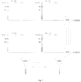
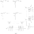
- Fig. 1 it represents the schematic of the pinout of a general Matrix Output Device (MOD) with "m” rows and “n” columns, which is the target for the solution given by the present invention.
- the matrix outputs are current sources, thus, these were labeled accordingly and enumerated in the typical matrix form as Source(i, j), where “i” ranges from 1 to “m” and “j” ranges from 1 to "n".
- Source(i, j) a general Matrix Output Device
- Fig. 2a is a PSPMT with 8 rows and 8 columns (64 outputs), while Fig. 2b is a SiPMA with 16 rows and 16 columns (256 outputs). Both are examples of matrix output devices and have output sets as shown in Fig. 1 , which may benefit from the present invention in order to reduce the number of electronic channels required to reproduce the coordinates of the gamma rays detected at the scintillators coupled to these MODs.
- Each matrix element of the SiPMA is a SiPM that requires its own biasing as can be seen in Fig. 3a and Fig. 3b .
- the SiPM element Dij has a symbol of diode. It is biased in reversed polarity from Vcc across a limiting resistor Rp(ij).
- the capacitor Cp(i j) holds sufficient charge to provide the output current when the SiPM opens after a nuclear event appears.
- the output labeled as Source(i, j) in the circuit of Fig. 3a requires a low impedance current mode connection, while the same output in the circuit of Fig. 3b requires voltage mode connection, because this latter one includes the resistor Rg(ij), which drains the SiPM current, producing a voltage source instead of a current.
- Our goal is to provide a readout network to deal with the uncountable MODs outputs (labeled in the form Source(i, j) in Fig. 1 , where “i” ranges from 1 to “m” and “j” ranges from 1 to "n", being “m” the number of rows and “n” the number of columns) and be able to reproduce the original coordinates of the impact in the scintillator, and doing it even for very noisy devices such as SiPMA.
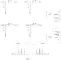
- a good way to filter the uncountable SiPMA outputs could be to include active filtering at any output, Source(i, j), but this normally will involve the use of a replicable circuit (as the one in Fig. 4a ) with the same number of OpAmps (m x n), which increases the circuit space, and power requirements, disregarding the cost. Furthermore, the number of filtered outputs is the same as the number of inputs (m x n), in such a way that, if we want to reduce them, we should include a further readout network (such as Popov, etc). That is why, an alternative circuit is proposed instead of replicating the circuit of Fig. 4a , for all the MOD outputs Source(i, j).
- This circuit shares the OpAmp labeled as AmplifierA, and the passive component at the feedback loop of the OpAmp, labeled as R_feedback, while includes separate passive components in the input side (Ci1r, Ci2r,...,Cinr in Fig. 4b and C1jc, C2jc,...,Cmjc in Fig. 4c ), receiving all the separate noisy signals (Source(i,1), to Source(i,n) in Fig. 4b and Source(1,j), to Source(m,j) in Fig. 4c ) and injecting their currents together (added) in the negative input of the single OpAmp labeled as AmplifierA in both cases.
- this filtering circuit may be of the type (CijrRijr or CijcRijc) shown in Fig. 5b or (CijrLijr or CijcLijc) shown in Fig. 5c , and thus represented as generic boxes - Fijc, Fijr in Fig. 5a - too.
- the filtering circuits working together with the OpAmp circuits conform an equivalent "active filter network" with the ability to attenuate the noisy signals reaching the readout network inputs from the MOD outputs Source(i, j), while the real signals from nuclear events are passed through the circuitry without attenuation and are symmetrically directed only to its specific "Row(i) output” and its specific "Column(j) output", without interfering with each other and further amplified to generate the corresponding amplified and filtered signals AmpRow(i) and AmpCol.(j).
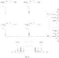
- the filtering circuit is composed by a Capacitor in series with a Resistor, to conform the filtering block shown in Fig. 5b . It is easy to obtain the new circuit from Fig. 6 , by replacing the general filtering block (as Fig. 5a ), attached to each Source(i, j), by the specific "CR based" filtering circuit of Fig. 5b . The result is the schematic of the Fig. 7 .
- the signals from a specific MOD output, Source (i, j) are symmetrically divided in two components that will not interfere with each other, neither with any other arriving signal from a different MOD output.
- One of the two components is treated by the "High Pass filter” created by the passive components Cijc, Rijc and R_Feedback and the Amplifier with output AmpCol(j), (see Fig. 4c too).
- the cutting frequency of the filter is given by the parameter Cijc x R_Feedback, although the maximum gain is limited by the ratio R_Feedback / Rijc, to increase the circuit stability.
- the other one of the two components is treated by the "High Pass filter” created by the passive components Cijr, Rijr and R_Feedback and the Amplifier with output AmpRow(i), (see Fig. 4b too).
- the cutting frequency of the filter is given by the parameter Cijr x R_Feedback, although the maximum gain is limited by the ratio R_Feedback / Rijr, to increase the circuit stability.
- the filtering circuit is composed by a Capacitor in series with an Inductor, to conform the filtering block shown in Fig. 5c . It is easy to obtain the new circuit from Fig. 6 , by replacing the general filtering block (as Fig. 5a ), attached to each Source(i, j), by the specific "CL based" filtering circuit of Fig. 5c . The result is the schematic of the Fig. 8 .
- the signals from a specific MOD output, Source (i, j) are symmetrically divided in two components that will not interfere with each other, neither with any other arriving signal from a different MOD output.
- One of the two signal components is treated by the "Band Pass filter” created by the passive components Cijc, Lijc and R_Feedback and the Amplifier with output AmpCol(j).
- the central frequency of the filter is given by the parameter Cijc x Lijc.
- Lijc has the parasitic resistance R(Lijc) which limits the maximum gain to the ratio R_Feedback / R(Lijc), to increase the circuit stability.
- the other one of the two signal component is treated by the "Band Pass filter” created by the passive components Cijr, Lijr and R_Feedback and the Amplifier with output AmpRow(i).
- the center frequency of the filter is given by the parameter Cijr x Lijr.
- the maximum gain is limited by the ratio R_Feedback / R(Lijr), increasing the circuit stability. Being R(Lijr) the parasitic resistance of the inductor Lijr.
- the SiPMA (or MOD in general) is optically coupled to a monolithic scintillator crystal.
- the readout network inputs (Source(i, j) (using the circuit of Fig. 7 ), "i” ranges 1 to m; “j” ranges 1 to n) are connected to the matrix outputs of the SiPMA (as seen in Fig. 1 also labeled as (Source(i, j)), and the two types of filtering circuit component outputs (divided in rows and columns) are connected to the low impedance inputs of the amplifiers that complete the active filtering functionality of the network.
- the amplified signals labeled as AmpRow(i) and AmpCol.
- the network outputs are the amplifiers outputs related to all Rows and Columns of the matrix, being Rows + Columns equal to the output channel number of the readout network. These outputs are located at the bottom and right sides of the schematic in Fig. 7 , and labeled as AmpRow(i) and AmpCol.(j).
- An alternative embodiment can be obtained from a previous preferred embodiment by replacing the circuit of Fig 7 by the circuit of Fig. 8 .
- the SiPMA is optically coupled to a monolithic scintillator crystal.
- the readout network inputs (Source(i, j) (using the circuit of Fig. 8 ), "i” ranges 1, to m; “j” ranges 1 to n) are connected to the matrix outputs of the SiPMA (as seen in Fig. 1 also labeled as (Source(i, j)), and the two types of filtering circuit component outputs (divided in rows and columns) are connected to the low impedance inputs of the amplifiers that complete the active filtering functionality of the network.
- the amplified signals labeled as AmpRow(i) and AmpCol.(j); (i ranges 1 to m and "j" ranges 1 to n) reach a number equal to the sum of columns and rows), and can be later processed analogically or digitally to obtain the planar impact position of the gamma ray in the monolithic crystal and the DOI if required.
- the network outputs are located here too at the bottom and right sides of the schematic in Fig. 8 , and labeled as AmpRow(i) and AmpCol.( j).
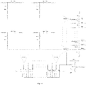
- an appropriated acquisition and digitizing electronics for the "m+n" channels is required and specific software to process all signals and provide planar positioning of the detected ray (gamma or X) and DOI if required.
- the amplified signals can be connected to a pair of divider resistor chains (one for Rows, shown at right side, and the other for Columns, shown at bottom side) to reduce the output quantity to 4 and be able to apply the COG algorithm.
- the resistor chain established to calculate X coordinate, located at bottom side, is labeled R0x, R1x, R2x, .., Rnx, and the outputs at its edges are labeled "X-" and "X+ ".
- the resistor chain established to calculate Y coordinate, located at right side is labeled R0y, R1y, R2y, .., Rmy, and the outputs at its edges are labeled "Y-" and "Y+ ".
- the gamma rays impinging the scintillator will produce a distribution of light over the SiPMA, activating a lot of SiPMs each time, which allows obtaining, not only the planar coordinates where the gamma ray reaches the scintillator, but also the DOI of the gamma ray inside the scintillator.
- This task can be done on real time, applying the analog processing described by [Christoph] and digitizing just one signal representing the DOI, or can be accomplished reading and digitizing the individuals signals of every row and column and determining the light shape and its corresponding DOI.
- a further pair of resistor chains can be connected by the input side to the nodes of both previous resistor chains (tied to all AmpRows(i) and AmpCol. (j) outputs) and can be connected by the output side to an electronic adding circuit (labeled AmpB) that makes up all the voltages at those nodes to obtain analogically an additional signal representing DOI and labeled as DOI Signal.
Landscapes
- Health & Medical Sciences (AREA)
- Physics & Mathematics (AREA)
- Life Sciences & Earth Sciences (AREA)
- General Physics & Mathematics (AREA)
- High Energy & Nuclear Physics (AREA)
- Molecular Biology (AREA)
- Spectroscopy & Molecular Physics (AREA)
- Engineering & Computer Science (AREA)
- Multimedia (AREA)
- Signal Processing (AREA)
- Biomedical Technology (AREA)
- Nuclear Medicine, Radiotherapy & Molecular Imaging (AREA)
- Optics & Photonics (AREA)
- Medical Informatics (AREA)
- General Health & Medical Sciences (AREA)
- Measurement Of Radiation (AREA)
- Power Engineering (AREA)
- Nuclear Medicine (AREA)
- Data Exchanges In Wide-Area Networks (AREA)
Applications Claiming Priority (2)
| Application Number | Priority Date | Filing Date | Title |
|---|---|---|---|
| ES201531953A ES2629096B1 (es) | 2015-12-31 | 2015-12-31 | Topología de red de lectura |
| PCT/ES2016/070950 WO2017114998A1 (es) | 2015-12-31 | 2016-12-30 | Topología de red de lectura |
Publications (3)
| Publication Number | Publication Date |
|---|---|
| EP3399345A1 true EP3399345A1 (de) | 2018-11-07 |
| EP3399345A4 EP3399345A4 (de) | 2019-08-14 |
| EP3399345B1 EP3399345B1 (de) | 2023-10-11 |
Family
ID=59224672
Family Applications (1)
| Application Number | Title | Priority Date | Filing Date |
|---|---|---|---|
| EP16881321.0A Active EP3399345B1 (de) | 2015-12-31 | 2016-12-30 | Lesenetzwerktopologie |
Country Status (4)
| Country | Link |
|---|---|
| US (1) | US10838084B2 (de) |
| EP (1) | EP3399345B1 (de) |
| ES (1) | ES2629096B1 (de) |
| WO (1) | WO2017114998A1 (de) |
Cited By (2)
| Publication number | Priority date | Publication date | Assignee | Title |
|---|---|---|---|---|
| IT202100004655A1 (it) * | 2021-03-01 | 2022-09-01 | Consiglio Nazionale Ricerche | Dispositivo di rilevazione scintigrafica con area estesa |
| ES2939157A1 (es) * | 2021-10-12 | 2023-04-19 | General Equipment For Medical Imaging S A | Topologia de red de lectura para dispositivos de tomografia por emision de positrones con tiempo de vuelo |
Families Citing this family (1)
| Publication number | Priority date | Publication date | Assignee | Title |
|---|---|---|---|---|
| CN111245378B (zh) * | 2020-01-13 | 2023-06-16 | 江苏赛诺格兰医疗科技有限公司 | 一种用于pet系统中探测器的加法电路 |
Family Cites Families (12)
| Publication number | Priority date | Publication date | Assignee | Title |
|---|---|---|---|---|
| DE2154539C3 (de) * | 1971-11-03 | 1974-10-10 | Philips Patentverwaltung Gmbh, 2000 Hamburg | Belichtungsautomaten-Schaltung eines Röntgendiagnostikapparates |
| US4622467A (en) * | 1982-04-21 | 1986-11-11 | California Institute Of Technology | System for mapping radioactive specimens |
| US5347590A (en) * | 1991-06-10 | 1994-09-13 | General Electric Company | Spatial filter for an image processing system |
| US5708269A (en) * | 1995-08-15 | 1998-01-13 | Raytheon Ti Systems, Inc. | Thermal detector and method |
| US6747263B1 (en) * | 2001-12-07 | 2004-06-08 | Southeastern University Research Assn. Inc. | Matrix output device readout system |
| ES2239506B1 (es) | 2003-04-10 | 2006-11-16 | Consejo Superior Investigacion | Detector de rayos gamma con codificacion de profundidad de interaccion. |
| GB2451678A (en) * | 2007-08-10 | 2009-02-11 | Sensl Technologies Ltd | Silicon photomultiplier circuitry for minimal onset and recovery times |
| US8884240B1 (en) * | 2009-06-08 | 2014-11-11 | Radiation Monitoring Devices, Inc. | Position sensitive solid-state photomultipliers, systems and methods |
| DE102012000702B3 (de) * | 2012-01-16 | 2013-02-21 | Karlsruher Institut für Technologie | Optische Kohärenztomographie mit erweitertem Dynamikbereich |
| US9106191B2 (en) * | 2012-05-02 | 2015-08-11 | Adaptive I/O Technologies, Inc. | Diode enhanced amplifier circuits and methods thereof |
| US8886697B2 (en) * | 2012-12-28 | 2014-11-11 | General Electric Company | Solid state photomultiplier with improved pulse shape readout |
| US10527740B2 (en) * | 2014-04-03 | 2020-01-07 | Siemens Medical Solutions Usa, Inc. | Silicon photomultiplier based TOF-PET detector |
-
2015
- 2015-12-31 ES ES201531953A patent/ES2629096B1/es active Active
-
2016
- 2016-12-30 WO PCT/ES2016/070950 patent/WO2017114998A1/es not_active Ceased
- 2016-12-30 EP EP16881321.0A patent/EP3399345B1/de active Active
-
2018
- 2018-06-28 US US16/021,370 patent/US10838084B2/en active Active
Cited By (5)
| Publication number | Priority date | Publication date | Assignee | Title |
|---|---|---|---|---|
| IT202100004655A1 (it) * | 2021-03-01 | 2022-09-01 | Consiglio Nazionale Ricerche | Dispositivo di rilevazione scintigrafica con area estesa |
| WO2022185147A1 (en) * | 2021-03-01 | 2022-09-09 | Consiglio Nazionale Delle Ricerche | Scintigraphic measurement device with extended area |
| US20240230931A9 (en) * | 2021-03-01 | 2024-07-11 | Consiglio Nazionale Delle Ricerche | Scintigraphic measurement device with extended area |
| ES2939157A1 (es) * | 2021-10-12 | 2023-04-19 | General Equipment For Medical Imaging S A | Topologia de red de lectura para dispositivos de tomografia por emision de positrones con tiempo de vuelo |
| WO2023062263A1 (es) * | 2021-10-12 | 2023-04-20 | General Equipment For Medical Imaging S.A. | Topología de red de lectura para dispositivos de tomografía por emisión de positrones con tiempo de vuelo |
Also Published As
| Publication number | Publication date |
|---|---|
| WO2017114998A4 (es) | 2017-08-31 |
| WO2017114998A8 (es) | 2017-10-19 |
| US20190004188A1 (en) | 2019-01-03 |
| EP3399345A4 (de) | 2019-08-14 |
| ES2629096A1 (es) | 2017-08-07 |
| WO2017114998A1 (es) | 2017-07-06 |
| EP3399345B1 (de) | 2023-10-11 |
| ES2629096B1 (es) | 2018-10-26 |
| US10838084B2 (en) | 2020-11-17 |
Similar Documents
| Publication | Publication Date | Title |
|---|---|---|
| US11828891B2 (en) | Silicon photomultiplier based TOF-PET detector | |
| EP2989487B1 (de) | Erfassung von strahlungsquanten anhand eines optischen detektors aus pixelzellen und pixelzelltriggerschaltung | |
| CN105765405B (zh) | 用于探测光子的探测设备和其方法 | |
| US9720109B2 (en) | Systems and methods for minimizing silicon photomultiplier signal propagation delay dispersion and improve timing | |
| Popov et al. | Analog readout system with charge division type output | |
| US10838084B2 (en) | Read network topology | |
| Zou et al. | Planar CMOS analog SiPMs: Design, modeling, and characterization | |
| US10128801B2 (en) | Bootstrapping readout for large terminal capacitance analog-SiPM based time-of-flight PET detector | |
| CN1971652B (zh) | 用于处理检测器信号的方法和装置 | |
| Marano et al. | A new simple and effective procedure for SiPM electrical parameter extraction | |
| CN110118600B (zh) | 信号处理电路和包括该信号处理电路的光电探测系统 | |
| CN111245378B (zh) | 一种用于pet系统中探测器的加法电路 | |
| KR20150088607A (ko) | 방사선 검출기 | |
| US7495201B2 (en) | Charge multiplexed array of solid-state photosensitive detectors | |
| EP2381475B1 (de) | Verfahren zur Verwaltung eines Silizium-Fotovervielfacherbauelement | |
| Hernández Hernández et al. | Read network topology | |
| CN209820630U (zh) | 信号处理电路和包括该信号处理电路的光电探测系统 | |
| KR101815290B1 (ko) | 양극성 펄스를 이용한 멀티플렉싱 신호 처리 방법 | |
| Castoldi et al. | 256 Channel Antialiasing Filter with Selectable Parameters and Differential Input to be Coupled with the GET Frontend Electronics: Design and Performance | |
| CN113037221A (zh) | 用于SiPM读出系统的共基极前置放大网络电路及其读出方法 | |
| CN118645131A (zh) | 一种基于肖特基二极管的电阻网络子电路读出电路 | |
| Lau et al. | Noise analysis of LSO-PSAPD PET detector front-end multiplexing circuits | |
| Carniti et al. | The CLARO ASIC: Design and performance of prototype integrated circuits for fast single photon counting at low power | |
| Belkacem et al. | PRELIMINARY DESIGN AND SIMULATION OF SIPM DEVICE OPERATION FOR A POTENTIAL CUBESAT RADIATION DETECTOR | |
| Dey et al. | Impact of analog IC impairments in SiPM interface electronics |
Legal Events
| Date | Code | Title | Description |
|---|---|---|---|
| STAA | Information on the status of an ep patent application or granted ep patent |
Free format text: STATUS: THE INTERNATIONAL PUBLICATION HAS BEEN MADE |
|
| PUAI | Public reference made under article 153(3) epc to a published international application that has entered the european phase |
Free format text: ORIGINAL CODE: 0009012 |
|
| STAA | Information on the status of an ep patent application or granted ep patent |
Free format text: STATUS: REQUEST FOR EXAMINATION WAS MADE |
|
| 17P | Request for examination filed |
Effective date: 20180728 |
|
| AK | Designated contracting states |
Kind code of ref document: A1 Designated state(s): AL AT BE BG CH CY CZ DE DK EE ES FI FR GB GR HR HU IE IS IT LI LT LU LV MC MK MT NL NO PL PT RO RS SE SI SK SM TR |
|
| AX | Request for extension of the european patent |
Extension state: BA ME |
|
| DAV | Request for validation of the european patent (deleted) | ||
| DAX | Request for extension of the european patent (deleted) | ||
| A4 | Supplementary search report drawn up and despatched |
Effective date: 20190717 |
|
| RIC1 | Information provided on ipc code assigned before grant |
Ipc: G01T 1/20 20060101ALI20190711BHEP Ipc: G01T 1/208 20060101AFI20190711BHEP |
|
| RAP1 | Party data changed (applicant data changed or rights of an application transferred) |
Owner name: GENERAL QUIPMENT FOR MEDICAL IMAGING S.A. Owner name: UNIVERSITAT POLITECNICA DE VALENCIA Owner name: BRUKER SWITZERLAND AG Owner name: CONSEJO SUPERIOR DE INVESTIGACIONES CIENTIFICAS (C |
|
| STAA | Information on the status of an ep patent application or granted ep patent |
Free format text: STATUS: EXAMINATION IS IN PROGRESS |
|
| 17Q | First examination report despatched |
Effective date: 20210708 |
|
| GRAP | Despatch of communication of intention to grant a patent |
Free format text: ORIGINAL CODE: EPIDOSNIGR1 |
|
| STAA | Information on the status of an ep patent application or granted ep patent |
Free format text: STATUS: GRANT OF PATENT IS INTENDED |
|
| INTG | Intention to grant announced |
Effective date: 20230502 |
|
| RAP3 | Party data changed (applicant data changed or rights of an application transferred) |
Owner name: BRUKER SWITZERLAND AG Owner name: UNIVERSITAT POLITECNICA DE VALENCIA Owner name: CONSEJO SUPERIOR DE INVESTIGACIONES CIENTIFICAS (CSIC) Owner name: GENERAL QUIPMENT FOR MEDICAL IMAGING S.A. |
|
| GRAS | Grant fee paid |
Free format text: ORIGINAL CODE: EPIDOSNIGR3 |
|
| GRAA | (expected) grant |
Free format text: ORIGINAL CODE: 0009210 |
|
| STAA | Information on the status of an ep patent application or granted ep patent |
Free format text: STATUS: THE PATENT HAS BEEN GRANTED |
|
| AK | Designated contracting states |
Kind code of ref document: B1 Designated state(s): AL AT BE BG CH CY CZ DE DK EE ES FI FR GB GR HR HU IE IS IT LI LT LU LV MC MK MT NL NO PL PT RO RS SE SI SK SM TR |
|
| REG | Reference to a national code |
Ref country code: GB Ref legal event code: FG4D |
|
| REG | Reference to a national code |
Ref country code: CH Ref legal event code: EP |
|
| P01 | Opt-out of the competence of the unified patent court (upc) registered |
Effective date: 20231004 |
|
| REG | Reference to a national code |
Ref country code: IE Ref legal event code: FG4D |
|
| REG | Reference to a national code |
Ref country code: DE Ref legal event code: R096 Ref document number: 602016083435 Country of ref document: DE |
|
| REG | Reference to a national code |
Ref country code: LT Ref legal event code: MG9D |
|
| REG | Reference to a national code |
Ref country code: NL Ref legal event code: MP Effective date: 20231011 |
|
| REG | Reference to a national code |
Ref country code: AT Ref legal event code: MK05 Ref document number: 1620760 Country of ref document: AT Kind code of ref document: T Effective date: 20231011 |
|
| PG25 | Lapsed in a contracting state [announced via postgrant information from national office to epo] |
Ref country code: NL Free format text: LAPSE BECAUSE OF FAILURE TO SUBMIT A TRANSLATION OF THE DESCRIPTION OR TO PAY THE FEE WITHIN THE PRESCRIBED TIME-LIMIT Effective date: 20231011 |
|
| PG25 | Lapsed in a contracting state [announced via postgrant information from national office to epo] |
Ref country code: IS Free format text: LAPSE BECAUSE OF FAILURE TO SUBMIT A TRANSLATION OF THE DESCRIPTION OR TO PAY THE FEE WITHIN THE PRESCRIBED TIME-LIMIT Effective date: 20240211 |
|
| PG25 | Lapsed in a contracting state [announced via postgrant information from national office to epo] |
Ref country code: LT Free format text: LAPSE BECAUSE OF FAILURE TO SUBMIT A TRANSLATION OF THE DESCRIPTION OR TO PAY THE FEE WITHIN THE PRESCRIBED TIME-LIMIT Effective date: 20231011 |
|
| PG25 | Lapsed in a contracting state [announced via postgrant information from national office to epo] |
Ref country code: AT Free format text: LAPSE BECAUSE OF FAILURE TO SUBMIT A TRANSLATION OF THE DESCRIPTION OR TO PAY THE FEE WITHIN THE PRESCRIBED TIME-LIMIT Effective date: 20231011 |
|
| PG25 | Lapsed in a contracting state [announced via postgrant information from national office to epo] |
Ref country code: ES Free format text: LAPSE BECAUSE OF FAILURE TO SUBMIT A TRANSLATION OF THE DESCRIPTION OR TO PAY THE FEE WITHIN THE PRESCRIBED TIME-LIMIT Effective date: 20231011 |
|
| PG25 | Lapsed in a contracting state [announced via postgrant information from national office to epo] |
Ref country code: LT Free format text: LAPSE BECAUSE OF FAILURE TO SUBMIT A TRANSLATION OF THE DESCRIPTION OR TO PAY THE FEE WITHIN THE PRESCRIBED TIME-LIMIT Effective date: 20231011 Ref country code: IS Free format text: LAPSE BECAUSE OF FAILURE TO SUBMIT A TRANSLATION OF THE DESCRIPTION OR TO PAY THE FEE WITHIN THE PRESCRIBED TIME-LIMIT Effective date: 20240211 Ref country code: ES Free format text: LAPSE BECAUSE OF FAILURE TO SUBMIT A TRANSLATION OF THE DESCRIPTION OR TO PAY THE FEE WITHIN THE PRESCRIBED TIME-LIMIT Effective date: 20231011 Ref country code: BG Free format text: LAPSE BECAUSE OF FAILURE TO SUBMIT A TRANSLATION OF THE DESCRIPTION OR TO PAY THE FEE WITHIN THE PRESCRIBED TIME-LIMIT Effective date: 20240111 Ref country code: AT Free format text: LAPSE BECAUSE OF FAILURE TO SUBMIT A TRANSLATION OF THE DESCRIPTION OR TO PAY THE FEE WITHIN THE PRESCRIBED TIME-LIMIT Effective date: 20231011 Ref country code: PT Free format text: LAPSE BECAUSE OF FAILURE TO SUBMIT A TRANSLATION OF THE DESCRIPTION OR TO PAY THE FEE WITHIN THE PRESCRIBED TIME-LIMIT Effective date: 20240212 |
|
| PG25 | Lapsed in a contracting state [announced via postgrant information from national office to epo] |
Ref country code: SE Free format text: LAPSE BECAUSE OF FAILURE TO SUBMIT A TRANSLATION OF THE DESCRIPTION OR TO PAY THE FEE WITHIN THE PRESCRIBED TIME-LIMIT Effective date: 20231011 Ref country code: RS Free format text: LAPSE BECAUSE OF FAILURE TO SUBMIT A TRANSLATION OF THE DESCRIPTION OR TO PAY THE FEE WITHIN THE PRESCRIBED TIME-LIMIT Effective date: 20231011 Ref country code: PL Free format text: LAPSE BECAUSE OF FAILURE TO SUBMIT A TRANSLATION OF THE DESCRIPTION OR TO PAY THE FEE WITHIN THE PRESCRIBED TIME-LIMIT Effective date: 20231011 Ref country code: NO Free format text: LAPSE BECAUSE OF FAILURE TO SUBMIT A TRANSLATION OF THE DESCRIPTION OR TO PAY THE FEE WITHIN THE PRESCRIBED TIME-LIMIT Effective date: 20240111 Ref country code: LV Free format text: LAPSE BECAUSE OF FAILURE TO SUBMIT A TRANSLATION OF THE DESCRIPTION OR TO PAY THE FEE WITHIN THE PRESCRIBED TIME-LIMIT Effective date: 20231011 Ref country code: HR Free format text: LAPSE BECAUSE OF FAILURE TO SUBMIT A TRANSLATION OF THE DESCRIPTION OR TO PAY THE FEE WITHIN THE PRESCRIBED TIME-LIMIT Effective date: 20231011 |
|
| PG25 | Lapsed in a contracting state [announced via postgrant information from national office to epo] |
Ref country code: DK Free format text: LAPSE BECAUSE OF FAILURE TO SUBMIT A TRANSLATION OF THE DESCRIPTION OR TO PAY THE FEE WITHIN THE PRESCRIBED TIME-LIMIT Effective date: 20231011 |
|
| REG | Reference to a national code |
Ref country code: DE Ref legal event code: R097 Ref document number: 602016083435 Country of ref document: DE |
|
| PG25 | Lapsed in a contracting state [announced via postgrant information from national office to epo] |
Ref country code: CZ Free format text: LAPSE BECAUSE OF FAILURE TO SUBMIT A TRANSLATION OF THE DESCRIPTION OR TO PAY THE FEE WITHIN THE PRESCRIBED TIME-LIMIT Effective date: 20231011 |
|
| PG25 | Lapsed in a contracting state [announced via postgrant information from national office to epo] |
Ref country code: SK Free format text: LAPSE BECAUSE OF FAILURE TO SUBMIT A TRANSLATION OF THE DESCRIPTION OR TO PAY THE FEE WITHIN THE PRESCRIBED TIME-LIMIT Effective date: 20231011 |
|
| PG25 | Lapsed in a contracting state [announced via postgrant information from national office to epo] |
Ref country code: SM Free format text: LAPSE BECAUSE OF FAILURE TO SUBMIT A TRANSLATION OF THE DESCRIPTION OR TO PAY THE FEE WITHIN THE PRESCRIBED TIME-LIMIT Effective date: 20231011 Ref country code: SK Free format text: LAPSE BECAUSE OF FAILURE TO SUBMIT A TRANSLATION OF THE DESCRIPTION OR TO PAY THE FEE WITHIN THE PRESCRIBED TIME-LIMIT Effective date: 20231011 Ref country code: RO Free format text: LAPSE BECAUSE OF FAILURE TO SUBMIT A TRANSLATION OF THE DESCRIPTION OR TO PAY THE FEE WITHIN THE PRESCRIBED TIME-LIMIT Effective date: 20231011 Ref country code: IT Free format text: LAPSE BECAUSE OF FAILURE TO SUBMIT A TRANSLATION OF THE DESCRIPTION OR TO PAY THE FEE WITHIN THE PRESCRIBED TIME-LIMIT Effective date: 20231011 Ref country code: EE Free format text: LAPSE BECAUSE OF FAILURE TO SUBMIT A TRANSLATION OF THE DESCRIPTION OR TO PAY THE FEE WITHIN THE PRESCRIBED TIME-LIMIT Effective date: 20231011 Ref country code: DK Free format text: LAPSE BECAUSE OF FAILURE TO SUBMIT A TRANSLATION OF THE DESCRIPTION OR TO PAY THE FEE WITHIN THE PRESCRIBED TIME-LIMIT Effective date: 20231011 Ref country code: CZ Free format text: LAPSE BECAUSE OF FAILURE TO SUBMIT A TRANSLATION OF THE DESCRIPTION OR TO PAY THE FEE WITHIN THE PRESCRIBED TIME-LIMIT Effective date: 20231011 |
|
| REG | Reference to a national code |
Ref country code: CH Ref legal event code: PL |
|
| PLBE | No opposition filed within time limit |
Free format text: ORIGINAL CODE: 0009261 |
|
| STAA | Information on the status of an ep patent application or granted ep patent |
Free format text: STATUS: NO OPPOSITION FILED WITHIN TIME LIMIT |
|
| PG25 | Lapsed in a contracting state [announced via postgrant information from national office to epo] |
Ref country code: LU Free format text: LAPSE BECAUSE OF NON-PAYMENT OF DUE FEES Effective date: 20231230 |
|
| PG25 | Lapsed in a contracting state [announced via postgrant information from national office to epo] |
Ref country code: MC Free format text: LAPSE BECAUSE OF FAILURE TO SUBMIT A TRANSLATION OF THE DESCRIPTION OR TO PAY THE FEE WITHIN THE PRESCRIBED TIME-LIMIT Effective date: 20231011 |
|
| REG | Reference to a national code |
Ref country code: BE Ref legal event code: MM Effective date: 20231231 |
|
| PG25 | Lapsed in a contracting state [announced via postgrant information from national office to epo] |
Ref country code: MC Free format text: LAPSE BECAUSE OF FAILURE TO SUBMIT A TRANSLATION OF THE DESCRIPTION OR TO PAY THE FEE WITHIN THE PRESCRIBED TIME-LIMIT Effective date: 20231011 Ref country code: LU Free format text: LAPSE BECAUSE OF NON-PAYMENT OF DUE FEES Effective date: 20231230 |
|
| 26N | No opposition filed |
Effective date: 20240712 |
|
| REG | Reference to a national code |
Ref country code: IE Ref legal event code: MM4A |
|
| PG25 | Lapsed in a contracting state [announced via postgrant information from national office to epo] |
Ref country code: IE Free format text: LAPSE BECAUSE OF NON-PAYMENT OF DUE FEES Effective date: 20231230 |
|
| PG25 | Lapsed in a contracting state [announced via postgrant information from national office to epo] |
Ref country code: BE Free format text: LAPSE BECAUSE OF NON-PAYMENT OF DUE FEES Effective date: 20231231 |
|
| PG25 | Lapsed in a contracting state [announced via postgrant information from national office to epo] |
Ref country code: CH Free format text: LAPSE BECAUSE OF NON-PAYMENT OF DUE FEES Effective date: 20231231 |
|
| PG25 | Lapsed in a contracting state [announced via postgrant information from national office to epo] |
Ref country code: SI Free format text: LAPSE BECAUSE OF FAILURE TO SUBMIT A TRANSLATION OF THE DESCRIPTION OR TO PAY THE FEE WITHIN THE PRESCRIBED TIME-LIMIT Effective date: 20231011 |
|
| PG25 | Lapsed in a contracting state [announced via postgrant information from national office to epo] |
Ref country code: SI Free format text: LAPSE BECAUSE OF FAILURE TO SUBMIT A TRANSLATION OF THE DESCRIPTION OR TO PAY THE FEE WITHIN THE PRESCRIBED TIME-LIMIT Effective date: 20231011 Ref country code: IE Free format text: LAPSE BECAUSE OF NON-PAYMENT OF DUE FEES Effective date: 20231230 Ref country code: CH Free format text: LAPSE BECAUSE OF NON-PAYMENT OF DUE FEES Effective date: 20231231 Ref country code: BE Free format text: LAPSE BECAUSE OF NON-PAYMENT OF DUE FEES Effective date: 20231231 |
|
| PG25 | Lapsed in a contracting state [announced via postgrant information from national office to epo] |
Ref country code: FI Free format text: LAPSE BECAUSE OF FAILURE TO SUBMIT A TRANSLATION OF THE DESCRIPTION OR TO PAY THE FEE WITHIN THE PRESCRIBED TIME-LIMIT Effective date: 20231011 |
|
| PG25 | Lapsed in a contracting state [announced via postgrant information from national office to epo] |
Ref country code: CY Free format text: LAPSE BECAUSE OF FAILURE TO SUBMIT A TRANSLATION OF THE DESCRIPTION OR TO PAY THE FEE WITHIN THE PRESCRIBED TIME-LIMIT; INVALID AB INITIO Effective date: 20161230 |
|
| PG25 | Lapsed in a contracting state [announced via postgrant information from national office to epo] |
Ref country code: HU Free format text: LAPSE BECAUSE OF FAILURE TO SUBMIT A TRANSLATION OF THE DESCRIPTION OR TO PAY THE FEE WITHIN THE PRESCRIBED TIME-LIMIT; INVALID AB INITIO Effective date: 20161230 |
|
| PG25 | Lapsed in a contracting state [announced via postgrant information from national office to epo] |
Ref country code: GR Free format text: LAPSE BECAUSE OF FAILURE TO SUBMIT A TRANSLATION OF THE DESCRIPTION OR TO PAY THE FEE WITHIN THE PRESCRIBED TIME-LIMIT; INVALID AB INITIO Effective date: 20161230 |
|
| PG25 | Lapsed in a contracting state [announced via postgrant information from national office to epo] |
Ref country code: TR Free format text: LAPSE BECAUSE OF FAILURE TO SUBMIT A TRANSLATION OF THE DESCRIPTION OR TO PAY THE FEE WITHIN THE PRESCRIBED TIME-LIMIT Effective date: 20231011 |
|
| PGFP | Annual fee paid to national office [announced via postgrant information from national office to epo] |
Ref country code: DE Payment date: 20251218 Year of fee payment: 10 |
|
| PGFP | Annual fee paid to national office [announced via postgrant information from national office to epo] |
Ref country code: GB Payment date: 20251216 Year of fee payment: 10 |
|
| PGFP | Annual fee paid to national office [announced via postgrant information from national office to epo] |
Ref country code: FR Payment date: 20251216 Year of fee payment: 10 |