EP3398238B1 - Wireless power transfer device and method - Google Patents
Wireless power transfer device and method Download PDFInfo
- Publication number
- EP3398238B1 EP3398238B1 EP16816129.7A EP16816129A EP3398238B1 EP 3398238 B1 EP3398238 B1 EP 3398238B1 EP 16816129 A EP16816129 A EP 16816129A EP 3398238 B1 EP3398238 B1 EP 3398238B1
- Authority
- EP
- European Patent Office
- Prior art keywords
- coil
- power transfer
- electronic processor
- transfer device
- wireless power
- Prior art date
- Legal status (The legal status is an assumption and is not a legal conclusion. Google has not performed a legal analysis and makes no representation as to the accuracy of the status listed.)
- Active
Links
Images









Classifications
-
- H—ELECTRICITY
- H02—GENERATION; CONVERSION OR DISTRIBUTION OF ELECTRIC POWER
- H02J—ELECTRIC POWER NETWORKS; CIRCUIT ARRANGEMENTS OR SYSTEMS FOR SUPPLYING OR DISTRIBUTING ELECTRIC POWER; SYSTEMS FOR STORING ELECTRIC ENERGY
- H02J50/00—Circuit arrangements or systems for wireless supply or distribution of electric power
- H02J50/10—Circuit arrangements or systems for wireless supply or distribution of electric power using inductive coupling
- H02J50/12—Circuit arrangements or systems for wireless supply or distribution of electric power using inductive coupling of the resonant type
-
- H—ELECTRICITY
- H02—GENERATION; CONVERSION OR DISTRIBUTION OF ELECTRIC POWER
- H02J—ELECTRIC POWER NETWORKS; CIRCUIT ARRANGEMENTS OR SYSTEMS FOR SUPPLYING OR DISTRIBUTING ELECTRIC POWER; SYSTEMS FOR STORING ELECTRIC ENERGY
- H02J4/00—Circuit arrangements for mains or distribution networks not specified as AC or DC; Circuit arrangements for mains or distribution networks combining AC and DC sections or sub-networks
- H02J4/20—Networks integrating separated AC and DC power sections
- H02J4/25—Networks integrating separated AC and DC power sections for transfer of electric power between AC and DC networks, e.g. for supplying the DC section within a load from an AC mains system
-
- H—ELECTRICITY
- H02—GENERATION; CONVERSION OR DISTRIBUTION OF ELECTRIC POWER
- H02J—ELECTRIC POWER NETWORKS; CIRCUIT ARRANGEMENTS OR SYSTEMS FOR SUPPLYING OR DISTRIBUTING ELECTRIC POWER; SYSTEMS FOR STORING ELECTRIC ENERGY
- H02J50/00—Circuit arrangements or systems for wireless supply or distribution of electric power
- H02J50/005—Mechanical details of housing or structure aiming to accommodate the power transfer means, e.g. mechanical integration of coils, antennas or transducers into emitting or receiving devices
-
- H—ELECTRICITY
- H02—GENERATION; CONVERSION OR DISTRIBUTION OF ELECTRIC POWER
- H02J—ELECTRIC POWER NETWORKS; CIRCUIT ARRANGEMENTS OR SYSTEMS FOR SUPPLYING OR DISTRIBUTING ELECTRIC POWER; SYSTEMS FOR STORING ELECTRIC ENERGY
- H02J50/00—Circuit arrangements or systems for wireless supply or distribution of electric power
- H02J50/40—Circuit arrangements or systems for wireless supply or distribution of electric power using two or more transmitting or receiving devices
-
- H—ELECTRICITY
- H02—GENERATION; CONVERSION OR DISTRIBUTION OF ELECTRIC POWER
- H02J—ELECTRIC POWER NETWORKS; CIRCUIT ARRANGEMENTS OR SYSTEMS FOR SUPPLYING OR DISTRIBUTING ELECTRIC POWER; SYSTEMS FOR STORING ELECTRIC ENERGY
- H02J50/00—Circuit arrangements or systems for wireless supply or distribution of electric power
- H02J50/90—Circuit arrangements or systems for wireless supply or distribution of electric power involving detection or optimisation of position, e.g. alignment
-
- H—ELECTRICITY
- H03—ELECTRONIC CIRCUITRY
- H03H—IMPEDANCE NETWORKS, e.g. RESONANT CIRCUITS; RESONATORS
- H03H7/00—Multiple-port networks comprising only passive electrical elements as network components
- H03H7/38—Impedance-matching networks
-
- H—ELECTRICITY
- H04—ELECTRIC COMMUNICATION TECHNIQUE
- H04B—TRANSMISSION
- H04B5/00—Near-field transmission systems, e.g. inductive or capacitive transmission systems
- H04B5/20—Near-field transmission systems, e.g. inductive or capacitive transmission systems characterised by the transmission technique; characterised by the transmission medium
- H04B5/24—Inductive coupling
- H04B5/26—Inductive coupling using coils
- H04B5/263—Multiple coils at either side
-
- H—ELECTRICITY
- H04—ELECTRIC COMMUNICATION TECHNIQUE
- H04B—TRANSMISSION
- H04B5/00—Near-field transmission systems, e.g. inductive or capacitive transmission systems
- H04B5/70—Near-field transmission systems, e.g. inductive or capacitive transmission systems specially adapted for specific purposes
- H04B5/79—Near-field transmission systems, e.g. inductive or capacitive transmission systems specially adapted for specific purposes for data transfer in combination with power transfer
Definitions
- Wireless power transfer may be achieved in a number of ways.
- One wireless power transfer technology is magnetic-resonance power transfer.
- WO2015/175096A1 (Qualcomm Incorporated) provides a structure that comprises two coils.
- the coils and an accompanying ferromagnetic layer are designed to have a low overall height.
- the ferromagnetic layer provides a large area underneath all of both coils, and may be constructed of tiles.
- At least one portion of the ferromagnetic layer has a reduced thickness, and provides a recess in the ferromagnetic layer.
- a first coil has at least one portion countersunk into the portion of the ferromagnetic layer that has the reduced thickness.
- a second coil overlaps the at least one countersunk portion of the first coil.
- the structure of WO2015/175096A1 is designed to charge a vehicle that is to be parked above the coils.
- WO2015/175096A1 proposes a particular shape of the coils.
- a receive coil of the vehicle may be misaligned with the common axis of the first and second coils by a certain distance, which is referred to in WO2015/175096A1 as an 'offset distance'.
- WO2015/175096A1 proposes to elongate the shape of the parts of the first and second coils where the second coil overlaps the at least one countersunk portion of the first coil.
- the elongation of the coils is in a direction that is perpendicular to the common axis of the coils.
- the extent of the elongation of the coils is much greater than the offset distance by which the receive coil of the vehicle may be misaligned with the common axis of the first and second coils, see figure 8 of WO2015/175096A1 .
- WO2015/175096A1 chooses to substantially increase one physical dimension of the overlap region of the coils, in order to address the problem of a vehicle that is misaligned by a comparatively much smaller offset distance.
- WO2015/175096A1 is choosing a structural solution, i.e. a particular design geometry that involves the shapes of both coils being substantially elongated.
- One embodiment provides a wireless power transfer device that in one particular instance includes a first coil having a first portion.
- the first coil is configured to generate a magnetic field.
- the wireless power transfer device also includes a second coil having a second portion.
- the second coil is positioned with respect to the first coil such that the first portion of the first coil overlaps the second portion of the second coil in an overlap region.
- the wireless power transfer device also includes a power amplifier electrically coupled to one selected from a group consisting of the first coil and the second coil, and configured to output a drive signal.
- the wireless power transfer device further includes a flux concentrator aligned with the overlap region and configured to concentrate a magnetic flux of the magnetic field. Details of the embodiment of the wireless power transfer device are provided in appended independent claim 1.
- Another embodiment provides a method of wirelessly transferring power with a wireless power transfer device that includes a first coil, a second coil, a power amplifier, a switch network, and an electronic processor.
- the method includes overlapping a first portion of the first coil with a second portion of the second coil in an overlap region, aligning a flux concentrator with the overlap region, and generating, with the power amplifier, a drive signal.
- the method further includes receiving the drive signal by one selected from a group consisting of the first coil and the second coil, and generating, by one selected from the group consisting of the first coil and the second coil, a magnetic field in response to receiving the drive signal. Details of the embodiment of the method of wirelessly transferring power are provided in appended independent claim 14.
- FIG. 1 illustrates a wireless power transfer system 100 including a wireless power transfer device 105 and an external device 110.
- the external device 110 includes, among other things, a receiver coil 113.
- the receiver coil 113 magnetically couples to the wireless power transfer device 105 to receive electrical power from the wireless power transfer device 105.
- the external device 110 may be, for example, a battery.
- the battery may be located in a smart telephone, a tablet computer, or other electrical device.
- the particular components of the external device 110 are not shown, but are understood by one of skill in the art.
- the wireless power transfer device 105 transfers power wirelessly to the external device 110 through magnetic resonance.
- a transmitter coil i.e., the coil transmitting power
- a receiver coil i.e., the coil receiving power
- a receiver coil i.e., the coil receiving power
- Power is transferred as a consequence of the receiver coil magnetically coupling to the transmitter coil.
- the efficiency of the power transfer is improved when the transmitter coil and the receiver coil have the same or similar size and form factor. However, in many applications it is not possible to match the size and form of the transmitter and receiver coils.
- a wireless battery charger may be designed to charge batteries having a receiver coil of a certain configuration, but batteries may be manufactured by many different entities and lack a uniform configuration.
- the wireless power transfer device 105 includes a first coil 115, a second coil 120, a switch network 125, a power amplifier 130, and an electronic processor 135.
- the wireless power transfer device 105 also includes a housing (not shown) that supports the first coil 115, the second coil 120, the switch network 125, the power amplifier 130, and the electronic processor 135.
- the wireless power transfer device 105 may include more or less components than those mentioned above.
- the first coil 115 includes a first looped wire having a first positive terminal 116 and a first negative terminal 118.
- the second coil 120 includes a second looped wire having a second positive terminal 122 and a second negative terminal 124.
- the first coil 115 and the second coil 120 are coupled to the switch network 125, and are configured to selectively and, in some cases, simultaneously, receive power from the power amplifier 130 according to a configuration of the switch network 125.
- the power amplifier 130 generates a drive signal that is provided to the first coil 115, the second coil 120, or both.
- the first coil 115 and the second coil 120 generate a magnetic field in response to receiving the drive signal from the power amplifier 130.
- the receiver coil 113 When the receiver coil 113 is within an applicable transmission range, the receiver coil 113 is magnetically coupled to the magnetic field generated by the first coil 115, the second coil 120, or both. As a consequence, electrical power is transferred from the wireless power transfer device 105 to the receiver coil 113.
- the first coil 115 has a first length 140 of, for example, approximately eighteen (18) centimeters (cm) and a first width 145 of, for example, approximately twelve (12) centimeters. It should be understood; however, that these dimensions (as well as other dimensions provided herein) are examples and different dimensions could be used.
- the first coil 115 also includes a first portion 150 located at a first longitudinal end 152 of the first coil 115 along the first width 145.
- the second coil 120 is substantially similar to the first coil 115.
- the second coil 120 has a second length 155 of approximately eighteen centimeters and a second width 160 of approximately twelve centimeters.
- the second coil 120 also includes a second portion 165 located at a second longitudinal end 147 of the second coil 120 along the second width 160. As shown in FIG. 2B , the second coil 120 is positioned such that the first portion 150 of the first coil 115 overlaps the second portion 165 of the second coil 120 in an overlap region 170. As shown in FIG. 2B , the size of the overlap region 170 is smaller than the size of the first coil 115 and smaller than the size of the second coil 120. In other words, the first coil 115 and the second coil 120 are only partially overlapped.
- the size (e.g., area and dimensions) of the overlap region 170 is not arbitrary, and is determined based on, for example, a geometry of the first coil 115, a geometry of the second coil 120, a number of turns of the first coil 115, a number of turns of the second coil 120, a width of turns of the first coil 115, a width of turns of the second coil 120, a spacing between the turns of the first coil 115, a spacing between the turns of the second coil 120, among other things.
- the overlap region 170 has a third length 175 of approximately two (2) centimeters and a third width 180 of approximately twelve centimeters. In other words, the first portion 150 overlaps the second portion 165 by approximately two centimeters.
- the overlapped first coil 115 and second coil 120 have an aggregate length 185 of approximately thirty-four (34) centimeters and an aggregate width 190 of approximately twelve centimeters.
- the overlap region 170 may have different dimensions based on particular dimensions of the first coil 115 and the second coil 120.
- the wireless power transfer device 105 also includes a flux concentrator 195 that concentrates the magnetic flux between the first coil 115 and the second coil 120.
- the flux concentrator 195 maximizes the magnetic flux coupling between the first coil 115 and the second coil 120 while minimizing magnetic losses in the coupling.
- the flux concentrator 195 is aligned with the overlap region 170 and positioned underneath the second coil 120, as shown in FIG. 2B . In this position, the flux concentrator 195, due to its material properties, can improve the return loss when the first coil 115 and the second coil 120 are magnetically coupled.
- the flux concentrator 195 includes a ferrite layer.
- the flux concentrator 195 also has a high permeability (e.g., 120) and low-loss factor (e.g., 0.017).
- the flux concentrator 195 has a first height 200 of approximately three tenths of a millimeter (0.3 mm).
- spacers 205a, 205b separate the first coil 115 from the second coil 120, and the second coil 120 from the flux concentrator 195.
- the spacers 205a, 205b include a passive material and are used to keep the first coil 115 and the second coil 120 an appropriate distance 207 apart.
- the spacers 205a, 205b include an insulating material having a second height 210 of approximately 2 mm.
- the spacers 205a, 205b use a microcellular urethane material by the name of PORON ®. In other embodiments, the spacers 205a, 205b may use other type of insulating material.
- the distance 207 between the first coil 115 and the second coil 120 is not arbitrary, and is determined based on, for example, the geometry of the first coil 115, the geometry of the second coil 120, the number of turns in the first coil 115, the number of turns in the second coil120, and the like.
- FIG. 3A shows the configuration of the overlap region 170 as described above with respect to FIGS. 2A and 2B .
- the overlap region 170 may be shaped and sized differently than the size and shape shown in FIGS. 2A and 2B .
- FIGS. 3B through 3D illustrate variations of the overlap region 170 and configurations of the first portion 150 of the first coil 115 and the second portion 165 of the second coil 120.
- FIG. 3B shows the first portion 150 of the first coil 115 located along the first length 140 of the first coil 115, and the second portion 165 of the second coil 120 located along the second length 155 of the second coil 120. Therefore, the overlap region 170 shown in FIG. 3B is positioned along the first length 140 of the first coil 115 and the second length 155 of the second coil 120.
- FIG. 3C illustrates the first portion 150 of the first coil 115 positioned along the first width 145 of the first coil 115, and the second portion 165 of the second coil 120 located along the second length 155 of the second coil 120.
- the overlap region 170 is positioned along the first width 145 of the first coil 115, and along the second length 155 of the second coil 120, thereby forming an L shaped overlap region 170.
- FIG. 3D illustrates the first portion 150 of the first coil 115 positioned along the first length 140 of the first coil 115, and the second portion 165 of the second coil 120 positioned along the second width 160 of the second coil 120.
- the overlap region 170 is positioned along the first length 140, and along the second width 160, thereby forming a T shaped overlap region 170.
- the first coil 115 as shown in FIG. 3C can be positioned centrally with respect to the second coil 120 such that a sideways T shape is formed instead of an L shape.
- the power transfer area is enlarged by expanding the size of a transmitter coil (i.e., the coil transmitting power from the wireless power transfer device 105).
- a transmitter coil i.e., the coil transmitting power from the wireless power transfer device 105.
- enlarging the power transfer area by expanding the size of a transmitter coil may lead to a mismatch of the size and form factor of the transmitter coil and the receiver coil 113 of the external device 110.
- the first coil 115, the second coil 120, and the switch network 125 uses the first coil 115, the second coil 120, and the switch network 125 to effectively enlarge the power transfer area of the wireless power transfer device 105 while minimizing the effects of a mismatch of the size or the form factor between a transmitter coil of the wireless power transfer device 105 (e.g., the first coil 115 or the second coil 120).
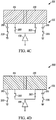
- FIGS. 4A through 4D illustrate various configurations of the switch network 125.
- the switch network 125 includes a plurality of switches to selectively detune the first coil 115, the second coil 120, or neither.
- the switch network 125 includes a first power switch 300, a second power switch 305, a first detuning component 310, a second detuning component 315, a first detuning switch 320, and a second detuning switch 325.
- the switch network 125 may include more or less switches and/or detuning components.
- the wireless power transfer device 105 may include more than two coils (e.g., a third coil), in which case the switch network 125 may also include additional switches and detuning components than the ones shown in FIGS. 4A through 4D .
- the first power switch 300 selectively electrically couples the first coil 115 to the power amplifier 130.
- the second power switch 305 selectively electrically couples the second coil 120 to the power amplifier 130.
- the first power switch 300 and the second power switch 305 are each switchable between a conducting state, in which the power amplifier 130 is electrically coupled to the first coil 115, and the second coil 120, respectively, and a non-conducting state, in which the power amplifier 130 is electrically decoupled (e.g., disconnected) from the first coil 115, and the second coil 120, respectively.
- the first detuning component 310 is selectively electrically coupled to the first coil 115 through the first detuning switch 320.
- the first detuning switch 320 is switchable between a conducting state in which the first coil 115 is electrically coupled to the first detuning component 310, and a non-conducting state in which the first coil 115 is decoupled (e.g., disconnected) from the first detuning component 310.
- the first detuning component 310 When the first detuning component 310 is electrically coupled to the first coil 115 (i.e., when the first detuning switch 320 is in the conducting state), the first detuning component 310 changes the resonant frequency of the first coil 115, which decreases the operability of the first coil 115 to transfer power to the external device 110. Therefore, when the first detuning component 310 is coupled to the first coil 115, the first detuning component 310 detunes the first coil 115. In some embodiments, the first detuning component 310 may change another characteristic of the first coil 115 and/or the magnetic field generated by the first coil 115 that decreases the operability of the first coil 115 to transfer power. In the illustrated embodiment, the first detuning component 310 includes a detuning capacitor. In other embodiments, other electrical components may be used that, when electrically coupled to the first coil 115, detune the first coil 115.
- the second detuning component 315 is selectively electrically coupled to the second coil 120 through the second detuning switch 325.
- the second detuning switch 325 is switchable between a conducting state in which the second coil 120 is electrically coupled to the second detuning component 315, and a non-conducting state in which the second coil 120 is decoupled (e.g., disconnected) from the second detuning component 315.
- the second detuning component 315 When the second detuning component 315 is electrically coupled to the second coil 120 (i.e., when the second detuning switch 325 is in the conducting state), the second detuning component 315 changes the resonant frequency of the second coil 120, or changes another characteristic of the second coil 120 and/or the magnetic field generated by the second coil 120 such that the operability of the second coil to transfer power is decreased. Therefore, when the second detuning component 315 is coupled to the second coil 20, the second detuning component 315 detunes the second coil 120.
- the second detuning component 315 includes a detuning capacitor. Components other than a capacitor may be used to detune the second coil 120.
- the switch network 125 Based on a state of the first and second power switches 300 and 305 and the first and second detuning switches 320 and 325, the switch network 125 selectively connects the power amplifier 130 to one of the first coil 115, or the second coil 120. As shown in FIGS. 4A through 4D , the switch network 125 can be placed in four different configurations.
- FIG. 4A illustrates a first configuration 327 of the switch network 125 in which the first power switch 300 is in the conducting state, the first detuning switch 320 is in the non-conducting state, the second power switch 305 is in the non-conducting state, and the second detuning switch 325 is in the conducting state.
- the power amplifier 130 is electrically coupled to the first coil 115 while the second coil 120 is detuned via the second detuning component 315. Therefore, the power amplifier 130 provides the drive signal to the first coil 115, and only the first coil 115 generates a magnetic field to transfer power to the receiver coil 113 of the external device 110.
- the first coil 115 is the transmitter coil (i.e., the coil receiving a drive signal from the power amplifier and, in response to the drive signal, generating the magnetic field to transfer power to the receiver coil 113) of the wireless power transfer device 105.
- FIG. 4B illustrates a second configuration 329 of the switch network 125 in which the first power switch 300 and the second detuning switch 325 are in the non-conducting state, and the first detuning switch 320 and the second power switch 305 are in the conducting state.
- the power amplifier 130 is electrically coupled to the second coil 120 while the first coil 115 is detuned via the first detuning component 310. Therefore, the power amplifier 130 provides the drive signal to the second coil 120, and only the second coil 120 generates a magnetic field to transfer power to the receiver coil 113 of the external device 110.
- the second coil 120 is the transmitter coil (i.e., the coil receiving a drive signal from the power amplifier and, in response to the drive signal, generating the magnetic field to transfer power to the receiver coil 113) of the wireless power transfer device 105.
- the switch network 125 When the switch network 125 is in the first configuration 327 or the second configuration 329, only one of the coils (e.g., the first coil 115 or the second coil 120) generates a magnetic field and transfers power to the external device 110 (e.g., is the transmitter coil). Therefore, when the switch network 125 operates in either the first configuration 327 or the second configuration 329, the switch network 125 is said to operate in an individual configuration in which either the first coil 115 or the second coil 120 is detuned.
- FIG. 4C illustrates a third configuration 331 of the switch network 125 in which the first power switch 300 is in the conducting state, while the second power switch 305, the first detuning switch 320, and the second detuning switch 325 are in the non-conducting state.
- the power amplifier 130 is electrically coupled to the first coil 115 and provides the drive signal to the first coil 115, which in response to receiving the drive signal, generates a first magnetic field.
- the second coil 120 since it is magnetically coupled to the first coil 115 and decoupled from the second detuning component 315, generates a second magnetic field in response to the first coil 115 generating the first magnetic field.
- both the first coil 115 and the second coil 120 transfer power to the external device 110, even though only the first coil 115 receives the drive signal from the power amplifier 130.
- the first coil 115 behaves as a transmitter coil (e.g., because the first coil 115 receives the drive signal from the power amplifier 130 and, in response, generates a first magnetic field)
- the second coil 120 behaves as a repeater coil (i.e., a coil that is magnetically coupled to a transmitter coil and that generates a magnetic field in response to the transmitter coil generating a magnetic field).
- FIG. 4D illustrates a fourth configuration 333 of the switch network 125 in which the second power switch 305 is in the conducting state while the first power switch 300, the first detuning switch 320, and the second detuning switch 325 are in the non-conducting state.
- the power amplifier 130 is electrically coupled to the second coil 120 and provides the drive signal to the second coil 120, which generates a magnetic field in response to receiving the drive signal.
- the first coil 115 since it is magnetically coupled to the second coil 120 and decoupled from the first detuning component 310, generates another magnetic field in response to the second coil 120 generating the magnetic field.
- both the first coil 115 and the second coil 120 transfer power to the external device 110, even though only the second coil 120 receives the drive signal from the power amplifier 130.
- the second coil 120 behaves as a transmitter coil (e.g., because the second coil 120 receives the drive signal from the power amplifier 130 and, in response, generates a magnetic field)
- the first coil 115 behaves as a repeater coil (i.e., because the first coil 115 is magnetically coupled to a transmitter coil (e.g., the second coil 120) and generates a magnetic field in response to the transmitter coil generating a magnetic field).
- both the first coil 115 and the second coil 120 When the switch network 125 operates in the third configuration 331 or the fourth configuration 333 both the first coil 115 and the second coil 120 generate a magnetic field, and both the first coil 115 and the second coil 120 can perform a power transfer operation (i.e., transfer power to the external device 110). Therefore, when the switch network 125 operates in either the third configuration 331 or the fourth configuration 333, the switch network 125 is said to operate in a combined configuration in which both the first coil 115 and the second coil 120 are tuned and can transfer power to the external device 110.
- the switch network 125 is electrically coupled to the electronic processor 135.
- the electronic processor 135 controls the state of each of the switches 300, 305, 320 and 325 in the switch network 125. In the illustrated embodiment, the electronic processor 135 determines which configuration to place the switch network 125 in based on a position of the receiver coil 113.
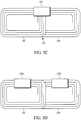
- one or more receiver coils 113 can be coupled to the wireless power transfer device 105.
- FIG. 5A shows a single receiver coil 113 positioned closest to the first coil 115.
- FIG. 5B shows a single receiver coil 113 positioned closest to the second coil 120.
- FIG. 5C shows a single receiver coil 113 positioned closest to the overlap region 170.
- FIG. 5A shows a single receiver coil 113 positioned closest to the first coil 115.
- FIG. 5B shows a single receiver coil 113 positioned closest to the second coil 120.
- FIG. 5C shows a single receiver coil 113 positioned closest to the overlap region 170.
- FIG. 5D shows a first receiver coil 113a positioned closest to the first coil 115 and a second receiver coil 113b positioned closest to the second coil 120.
- the receiver coil 113, the first receiver coil 113a, or the second receiver coil 113b are positioned "closest" to the first coil 115, the second coil 120, or the overlap region 170 relative to other positions of the receiver coil 113, the first receiver coil 113, or the second receiver coil 113b with respect to the wireless power transfer device 105.
- a receiver coil 113 may be positioned anywhere on a surface of the wireless power transfer device 105. While the receiver coil 113 remains on the surface of the wireless power transfer device 105, the receiver coil 113 may be positioned closer to, for example, the first coil 115, relative to the second coil 120 and relative to the overlap region 170.
- the switch network 125 When a single receiver coil 113 is positioned closest to the first coil 115, as shown in FIG. 5A , and the switch network 125 is in a combined configuration (i.e., both the first coil 115 and the second coil 120 transfer power), the power transferred by the second coil 120 remains unused because there is no external device positioned to receive the power from the second coil 120. Accordingly, the overall efficiency at which power is transferred from the wireless power transfer device 105 decreases when both the first coil 115 and the second coil 120 generate a magnetic field, but the receiver coil 113 is positioned to receive wireless power from only the first coil 115.
- the electronic processor 135 detects that only one receiver coil 113 is coupled to the wireless power transfer device 105, detects the position of the receiver coil 113, and places the switch network 125 in the appropriate individual configuration based on whether the receiver coil 113 is positioned closest to the first coil 115 or the second coil 120.
- the electronic processor 135 places the switch network 125 in a combined configuration when multiple receiver coils 113a, 113b ( FIG. 5D ) are coupled to the wireless power transfer device 105, thereby increasing the power transfer efficiency.
- the electronic processor 135 determines the position of the receiver coil 113 based on a first impedance associated with the first coil 115 and on a second impedance associated with the second coil 120.
- the impedance associated with the first coil 115 and the impedance associated with the second coil 120 refer to the apparent opposition in an electrical circuit to the flow of current.
- the receiver coil 113 approaches the first coil 115 (e.g., the receiver coil 113 magnetically couples to the first coil 115 because the external device 110 is placed closest to the first coil 115 relative to the second coil 120 and the overlap region 170, as shown in FIG. 5A )
- the first impedance associated with the first coil 115 decreases.
- the second impedance associated with the second coil 120 decreases.
- the electronic processor 135 monitors changes in the first impedance associated with the first coil 115 and the second impedance associated with the second coil 120. Detecting a change in the first impedance associated with the first coil 115 and/or the second impedance associated with the second coil 120 serves as an indication to the electronic processor 135 of the relative position of the receiver coil 113.
- the electronic processor 135 determines the position of the receiver coil 113, the electronic processor 135 controls the switch network 125 (i.e., controls the plurality of switches of the switch network 125) to place the switch network 125 in the first configuration 327, the second configuration 329, the third configuration 331, or the fourth configuration 333.
- the switch network 125 i.e., controls the plurality of switches of the switch network 125
- the electronic processor 135 determines that the receiver coil 113 is positioned closest to the first coil 115 relative to the second coil 120 and the overlap region 170 ( FIG. 5A ).
- the electronic processor 135 places the switch network 125 in the first configuration 327 (shown in FIG. 4A ).
- the electronic processor 135 determines that the receiver coil 113 is positioned closest to the second coil 120 relative to the first coil 115 and the overlap region 170, as shown in FIG. 5B
- the electronic processor 135 places the switch network 125 in the second configuration 329 (shown in FIG. 4B ).
- the electronic processor 135 determines that the receiver coil 113 is positioned closest to the overlap region 170 relative to the first coil 115 and the second coil 120 (as shown in FIG. 5C ), or that multiple receiver coils 113a, 113b are coupled to the wireless power transfer device 105 (as shown in FIG. 5D )
- the electronic processor 135 places the switch network 125 in either the third configuration 331 or the fourth configuration 333.
- FIG. 6 illustrates an exemplary method 340 implemented by the electronic processor 135 to determine the configuration for the switch network 125 based on a position of the receiver coil 113 (e.g., whether the receiver coil 113 is positioned closest to the first coil 115, the second coil 120, or the overlap region 170).
- the electronic processor 135 monitors a parameter of the first coil 115 and the second coil 120.
- the electronic processor 135 monitors the first impedance associated with the first coil 115 and the second impedance associated with the second coil 120.
- the electronic processor 135 may, additionally or alternatively, monitor other parameters associated with the first coil 115 and second coil 120 that help determine the relative position of the receiver coil 113. As shown in FIG. 6 , the electronic processor 135 periodically activates (e.g., by providing the drive signal from the power amplifier 130) the first coil 115 and/or the second coil 120 (block 345). Periodically powering the first coil 115 and the second coil 120 allows the electronic processor 135 to detect changes in the first impedance associated with the first coil 115 and the second impedance associated with the second coil 120.
- the electronic processor 135 monitors the first impedance associated with the first coil 115 and determines whether a first impedance change indicative of a decrease in the first impedance of the first coil 115 is detected by the electronic processor 135 (block 350). When the electronic processor 135 detects a change in the first impedance associated with the first coil 115 (e.g., a monitored parameter), the electronic processor 135 then determines whether a second impedance change indicative of a decrease in the second impedance associated with the second coil 120 is also detected (block 355).
- the electronic processor 135 detects the second impedance change at block 355 (i.e., detects both the first impedance change and the second impedance change)
- the electronic processor 135 activates both the first coil 115 and the second coil 120 (block 360) by placing the switch network 125 in a combined configuration (i.e., in either the third configuration 331 or the fourth configuration 333).
- the electronic processor 135 may detect a first impedance change and a second impedance change when the receiver coil 113 is positioned closest to the overlap region 170 (as shown in FIG. 5C ), or when a first receiver coil 113a is positioned closest to the first coil 115 and a second receiver coil 113b is positioned closest to the second coil 120 (as shown in FIG.
- the electronic processor 135 activates only the first coil 115 to transfer power (block 365) by placing the switch network 125 in the first configuration 327.
- the electronic processor 135 may detect the first impedance change, but not the second impedance change when the receiver coil 113 is positioned closest to the first coil 115 relative to the second coil 120 and the overlap region 170.
- the electronic processor 135 determines whether a second impedance change indicative of a decrease in the second impedance of the second coil 120 is detected (block 370). If the electronic processor 135 detects the second impedance change (i.e., only detects the second impedance change, but not the first impedance change), the electronic processor 135 activates only the second coil 120 for power transfer (block 375) by placing the switch network 125 in the second configuration 329.
- the electronic processor 135 may detect the second impedance change, but not the first impedance change when the receiver coil 113 is positioned closest to the second coil 120 relative to the first coil 115 and the overlap region 170. If, however, the second impedance change is not detected at block 370 (i.e., the electronic processor 135 does not detect the first impedance change or the second impedance change), the electronic processor 135 returns to block 345 to periodically activate the first coil 115 and the second coil 120 and thereby continue to monitor the first impedance associated with the first coil 115 and the second impedance associated with the second coil 120 for detection of an approaching receiver coil 113.
- the wireless power transfer device 105 may effectively change the size of the wireless power transfer area to maximize the power transfer efficiency.
- the wireless power transfer device 105 can activate a smaller wireless power transfer area (e.g., by activating only the first coil 115 or the second coil 120) when a single receiver coil 113 is coupled to the wireless power transfer device 105, and can activate an enlarged power transfer area (e.g., by activating both the first coil 115 and the second coil 120) when, for example, multiple receiver coils 113a, 113b are coupled to the wireless power transfer device 105.
- a smaller wireless power transfer area e.g., by activating only the first coil 115 or the second coil 120
- an enlarged power transfer area e.g., by activating both the first coil 115 and the second coil 120
- FIG. 7 illustrates a graph showing one example of the power transfer efficiency (e.g., a monitored efficiency) when a single receiver coil 113 is coupled to the wireless power transfer device 105 as shown in FIG. 5B , and the wireless power transfer device 105 does not detune the first coil 115.
- the power transfer efficiency is approximately equal to sixty percent (60%).
- the single receiver coil 113 is coupled to the wireless power transfer device 105 as shown in FIG.
- the wireless power transfer device 105 can achieve a greater power transfer efficiency.
- FIG. 8 is a flowchart illustrating the overall operation of the wireless power transfer device 105.
- the electronic processor 135 monitors the first impedance associated with the first coil 115 and second impedance associated with the second coil 120 (block 400).
- the electronic processor 135 determines whether a receiver coil 113 is coupled to the wireless power transfer device 105 based on the monitored impedance (block 405).
- the electronic processor 135 While the electronic processor 135 does not detect that a receiver coil 113 has coupled to the wireless power transfer device 105, the electronic processor 135 continues to monitor the first impedance associated with the first coil 115 and the second impedance associated with the second coil 120 (block 400). As discussed above, the electronic processor 135 monitors the first impedance associated with the first coil 115 and the second impedance associated with the second coil 120 by periodically and selectively activating the first coil 115 and the second coil 120.
- the electronic processor 135 detects that a receiver coil 113 has coupled to the wireless power transfer device 105, the electronic processor 135 determines the location of the receiver coil 113 at block 410 (i.e., determines whether the receiver coil 113 is positioned closest to the first coil 115, the second coil 120, or the overlap region 170). As discussed above, the electronic processor 135 determines the location of the receiver coil 113 based on the detected first impedance associated with the first coil 115 and second impedance associated with the second coil 120.
- the electronic processor 135 determines whether the receiver coil 113 is placed nearest the first coil 115, nearest the second coil 120, nearest the overlap region 170, and/or if multiple receiver coils 113a, 113b are coupled to the wireless power transfer device 105.
- the electronic processor 135 determines the location of the receiver coil 113, the electronic processor 135 places the switch network 125 in the appropriate configuration corresponding to the determined location of the receiver coil 113 (block 415).
- the wireless power transfer device 105 begins power transfer to the receiver coil 113 (block 420). While the wireless power transfer device 105 is transferring power to the receiver coil 113, the electronic processor 135 monitors the power transfer efficiency (e.g., an efficiency parameter of a power transfer operation) at block 425.
- the power transfer efficiency e.g., an efficiency parameter of a power transfer operation
- the electronic processor 135 may determine whether the receiver coil 113 has moved (e.g., from being nearest the first coil 115 to being nearest the second coil 120) and/or whether another receiver coil (e.g., a second receiver coil 113b) has been coupled to the wireless power transfer device 105 (block 430). If the electronic processor 135 determines that the receiver coil 113 has moved or that another receiver coil has coupled to the wireless power transfer device 105, the electronic processor 135 determines the new position of the receiver coil 113 and/or any additional receiver coils (block 435).
- the electronic processor 135 then updates the configuration of the switch network 125, if necessary, after the location of the receiver coil(s) 113 is determined (block 440) and proceeds to block 445. If, on the other hand, the electronic processor 135 determines that the receiver coil 113 has not moved and no additional receiver coils have been coupled to the wireless power transfer device 105, the electronic processor 135 jumps to block 445.
- the electronic processor 135 also determines whether or when the receiver coil(s) 113 are decoupled from the wireless power transfer device 105 (e.g., removed from the wireless power transfer device 105). When the electronic processor 135 determines that the receiver coil(s) 113 have been decoupled from the wireless power transfer device 105 , the electronic processor 135 returns to monitoring the first impedance associated with the first coil 115 and the second impedance associated with the second coil 120 to detect when a receiver coil 113 couples to the wireless power transfer device 105 (block 400).
- the electronic processor 135 determines that the receiver coil(s) 113 are still coupled to the wireless power transfer device 105, then the electronic processor 135 continues to monitor the power transfer efficiency to track the movement of the receiver coil(s) 113 while power transfer occurs (block 425).
- the electronic processor 135 monitors the power transfer efficiency of the power transfer operation performed by the wireless power transfer device 105, and determines, based on the power transfer efficiency, whether the receiver coil 113 has moved and/or whether a second receiver coil has been coupled to the wireless power transfer device 105.
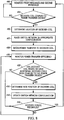
- FIG. 9 through FIG. 11 provide more details regarding the methods implemented by the electronic processor 135 to monitor the power transfer efficiency and track the movement of the receiver coil 113 based on the monitored power transfer efficiency.
- the method 448 is implemented by the electronic processor 135 when the electronic processor 135, based on the first impedance associated with the first coil 115 and the second impedance associated with the second coil 120, determines that the receiver coil 113 is positioned closest to the overlap region 170. Since the electronic processor 135 determines that the receiver coil 113 is nearest the overlap region 170, the electronic processor 135 activates the first coil 115 and the second coil 120 by placing the switch network in a combined configuration (block 450). The electronic processor 135 measures the power transfer efficiency when both the first coil 115 and the second coil 120 are activated (block 455).
- the electronic processor 135 then activates only the first coil 115 for a short duration (i.e., detunes the second coil 120 for the short duration) at block 460.
- the electronic processor 135 measures the power transfer efficiency when only the first coil 115 is activated (e.g., during the duration that only the first coil 115 is activated) at block 465.
- the electronic processor 135 compares the power transfer efficiencies by determining whether the power transfer efficiency associated with only the first coil 115 (e.g., a first transfer efficiency) is greater than the power transfer efficiency associated with both the first coil 115 and the second coil 120 (e.g., a second power transfer efficiency) at block 470.
- the electronic processor 135 determines that the power transfer efficiency associated with only the first coil 115 is greater than the power transfer efficiency associated with both the first coil 115 and the second coil 120, the electronic processor 135 determines that the receiver coil 113 has moved to be closer to the first coil 115 relative to the second coil 120 and the overlap region 170 (block 475), and activates the first coil 115 only (block 480) by placing the switch network 125 in the first configuration 327.
- the electronic processor 135 determines that the power transfer efficiency associated with both the first coil 115 and the second coil 120 being activated is greater than the power transfer efficiency associated with only the first coil 115 being activated, the electronic processor 135 then proceeds to determine whether a second receiver coil has been coupled to the wireless power transfer device 105 (block 485).
- the electronic processor 135 determines that a second receiver coil has been coupled to the wireless power transfer device by comparing a current power transfer efficiency with a previously measured power transfer efficiency. When a second receiver coil is coupled to the wireless power transfer device 105, the power transfer efficiency decreases significantly.
- the electronic processor 135 determines that a second receiver coil has coupled to the wireless power transfer device 105 when the electronic processor 135 detects a decrease in the currently measured power transfer efficiency relative to a previous power transfer efficiency.
- the electronic processor 135 determines that a second receiver coil has coupled to the wireless power transfer device 105, the electronic processor 135 continues to activate both the first coil 115 and the second coil 120 (block 490) by maintaining the switch network 125 in a combined configuration 331, 333. The electronic processor 135 then continues to monitor the power transfer efficiency to determine whether the number of receiver coils coupled to the power transfer device 105 has reduced and only one receiver coil 113 remains coupled to the wireless power transfer device 105 (block 495). If the electronic processor 135 determines that only one receiver coil 113 is coupled to the wireless power transfer device 105, the electronic processor 135 returns to block 450 to continue tracking the position of the receiver coil 113 by monitoring the power transfer efficiency and thereby determine an appropriate configuration for the switch network 125. If, however, the electronic processor 135 determines that multiple receiver coils are still coupled to the wireless power transfer device 105, the electronic processor 135 continues to activate the first coil 115 and the second coil 120 (block 490) by maintaining the switch network in a combined configuration.
- the electronic processor 135 determines that no additional receiver coils have coupled to the wireless power transfer device 105, the electronic processor 135 measures the power transfer efficiency when both the first coil 115 and the second coil 120 are activated (block 500). The electronic processor 135 then activates only the second coil 120 for a short duration (i.e., detunes the first coil 115 for the short duration) at block 505. The electronic processor 135 proceeds to measure the power transfer efficiency while only the second coil 120 is activated (block 510).
- the electronic processor 135 compares the power transfer efficiency when both the first coil 115 and the second coil 120 are activated with the power transfer efficiency when only the second coil 120 is activated by determining whether the power transfer efficiency associated with only the second coil 120 is greater than the power transfer efficiency associated with both the first coil 115 and the second coil 120 (block 515).
- the electronic processor 135 determines that the power transfer efficiency when only the second coil 120 is activated is greater than the power transfer efficiency when both the first coil 115 and the second coil 120 are activated, then the electronic processor 135 determines that the receiver coil 113 has moved to be closer to the second coil 120 relative to the first coil 115 and the overlap region 170 (block 520), and activates only the second coil 120 (block 525) by placing the switch network 125 in the second configuration 329.
- the electronic processor 135 determines that the power transfer efficiency when both the first coil 115 and the second coil 120 are activated is greater than the power transfer efficiency when only the second coil 120 is activated, the electronic processor 135 proceeds to determine whether a second receiver coil has been coupled to the wireless power transfer device 105 (block 530). The electronic processor 135 determines that a second receiver coil has coupled to the power transfer device 105 by comparing a currently measured power transfer efficiency with a previously measured power transfer efficiency, as discussed above with respect to block 485.
- the electronic processor 135 determines that a second receiver coil has coupled to the wireless power transfer device 105, the electronic processor 135 continues to activate both the first coil 115 and the second coil 120 (block 535) by maintaining the switch network 125 in a combined configuration. The electronic processor 135 then continues to monitor the power transfer efficiency to determine whether the number of receiver coils coupled to the power transfer device 105 has reduced to one and only one receiver coil 113 is coupled to the power transfer device 105 (block 540). If the electronic processor 135 determines that only one receiver coil 113 is coupled to the wireless power transfer device 105, the electronic processor 135 returns to block 450 to track the position of the receiver coil 113 by monitoring the power transfer efficiency.
- the electronic processor 135 determines that multiple receiver coils are still coupled to the wireless power transfer device 105, the electronic processor 135 continues to activate the first coil 115 and the second coil 120 (block 535) by maintaining the switch network 125 in a combined configuration 331, 333. Referring back to block 530, if the electronic processor 135 determines that no additional receiver coils have coupled to the power transfer device 105, the electronic processor 135 determines that the receiver coil 113 remains closest to the overlap region 170 relative to the first coil 115 and the second coil 120 (block 545), and returns to block 450 to activate both the first coil 115 and the second coil 120.
- the electronic processor 135 tracks the position of the receiver coil 113 and adjusts the configuration of the switch network 125 to maximize the power transfer efficiency and ensure the power is evenly distributed over a surface of the wireless power transfer device 105.
- the electronic processor 135 also determines whether additional receiver coils are coupled to the power transfer device 105 by monitoring the power transfer efficiency.
- FIG. 10 illustrates a method 598 of tracking the receiver coil 113 when the receiver coil 113 starts positioned closest to the first coil 115 of the wireless power transfer device 105 relative to the second coil 120 and the overlap region 170.
- the method 598 is implemented by the electronic processor 135 when the electronic processor 135, based on the first impedance associated with the first coil 115 and the second impedance associated with the second coil 120, determines that the receiver coil 113 is positioned closest to the first coil 115. Since the electronic processor 135 determines that the receiver coil 113 is closest to the first coil 115, the electronic processor 135 activates the first coil 115 only by placing the switch network in the first configuration 327 (block 600). Notably, when the electronic processor 135 determines, while tracking the receiver coil 113, that the receiver coil 113 moved closer to the first coil 115, as described in, for example, block 475, the electronic processor 135 jumps to block 600 and implements the method 598 described below.
- the electronic processor 135 measures the power transfer efficiency when only the first coil 115 is activated (block 605). To monitor the power transfer efficiency, the electronic processor 135 then activates both the first coil 115 and the second coil 120 for a short duration (block 610). The electronic processor 135 proceeds to measure the power transfer efficiency while both the first coil 115 and the second coil 120 are activated (block 615). The electronic processor 135 then returns the switch network 125 to the first configuration 327 such that only the first coil 115 is activated (block 620).
- the electronic processor 135 compares the power transfer efficiency associated with both the first coil 115 and the second coil 120 to the power transfer efficiency associated with only the first coil 115 by determining whether the power transfer efficiency associated with the first coil 115 is greater than the power transfer efficiency associated with the first coil 115 and the second coil 120 (block 625).
- the electronic processor 135 determines that the power transfer efficiency associated with only the first coil 115 is greater than the power transfer efficiency associated with both the first coil 115 and the second coil 120. If the electronic processor 135 determines that the receiver coil 113 remains positioned closest to the first coil 115 (block 630). The electronic processor 135 then continues to monitor the power transfer efficiency by periodically activating both the first coil 115 and the second coil 120 and measuring the power transfer efficiency (block 600 through block 625). If, however, the electronic processor 135 determines that the power transfer efficiency associated with both the first coil 115 and the second coil 120 is greater than the power transfer efficiency when only first coil 115 is activated, the electronic processor 135 proceeds to determine whether a second receiver coil has been coupled to the wireless power transfer device 105 (block 635).
- the electronic processor 135 determines that no additional receiver coils have been coupled to the wireless power transfer device 105, the electronic processor 135 assumes the receiver coil 113 has moved such that it is positioned closest to the overlap region 170 (block 640), which guides the electronic processor 135 to block 450 of FIG. 9A .
- the electronic processor 135 does not assume that the receiver coil 113 has moved closest to the overlap region 170. Instead, the electronic processor 135 measures the power transfer efficiency when only the first coil 115 is activated, measures the power transfer efficiency when only the second coil 120 is activated, and measures the power transfer efficiency when both the first coil 115 and the second coil 120 are activated. By comparing the three power transfer efficiencies, each associated with a different combination of the first coil 115 and the second coil 120 being activated, the electronic processor 135 may determine the position of the receiver coil 113 (e.g., whether the receiver coil 113 is positioned closest to the first coil 115, the second coil 120, or the overlap region 170).
- the electronic processor 135 determines that an additional receiver coil 113 has been coupled to the wireless power transfer device 105, the electronic processor 135 activates both the first coil 115 and the second coil 120 by placing the switch network 125 in a combined configuration (block 645). Then the electronic processor 135 continues to monitor the power transfer efficiency to determine whether the number of receiver coils coupled to the power transfer device 105 has reduced to one and determines whether only one receiver coil 113 is coupled to the wireless power transfer device 105 (block 650).
- the electronic processor 135 determines that only one receiver coil 113 is coupled to the wireless power transfer device 105, the electronic processor 135 assumes that the receiver coil 113 is positioned closest to the overlap region 170 (block 640) and returns to block 450 of FIG. 9A to determine the position of the receiver coil 113 more accurately.
- the electronic processor 135 determines that multiple receiver coils are still coupled to the wireless power transfer device 105, the electronic processor 135 continues to activate the first coil 115 and the second coil 120 by maintaining the switch network 125 in a combined configuration (block 645).
- FIG. 11 illustrates the method 698 of tracking the receiver coil 113 when the receiver coil 113 starts positioned closest to the second coil 120 of the wireless power transfer device 105 relative to the first coil 115 and the overlap region 170.
- the method 698 is implemented by the electronic processor 135 when the electronic processor 135, based on the first impedance associated with the first coil 115 and the second impedance associated with the second coil 120, determines that the receiver coil 113 is positioned closer to the second coil 120 than the first coil 115 or the overlap region 170. Since the electronic processor 135 determines that the receiver coil 113 is closest to the second coil 120, the electronic processor 135 activates only the second coil 120 by placing the switch network 125 in the second configuration 329 (block 700).
- the electronic processor 135 determines, while tracking the receiver coil 113, that the receiver coil 113 moved closer to the second coil 120 relative to the first coil 115 and the overlap region 170, as described, for example, in block 475 of FIG. 9A , the electronic processor 135 jumps to block 700 and implements the method 698 as described below.
- the electronic processor 135 measures the power transfer efficiency when only the second coil 120 is activated (block 705).
- the electronic processor 135 then activates both the first coil 115 and the second coil 120 for a short duration (block 710).
- the electronic processor 135 measures the power transfer efficiency while both the first coil 115 and the second coil 120 are activated (block 715).
- the electronic processor 135 returns the switch network 125 to the second configuration 329 such that only the second coil 120 is activated (block 720).
- the electronic processor 135 proceeds to compare the power transfer efficiency when both the first coil 115 and the second coil 120 are activated with the power transfer efficiency when only the second coil 120 is activated by determining whether the power transfer efficiency associated with the second coil 120 is greater than the power transfer efficiency associated with the first coil 115 and second coil 120 (block 725).
- the electronic processor 135 determines that the power transfer efficiency when only the second coil 120 is activated is greater than the power transfer efficiency when both the first coil 115 and the second coil 120 are activated, the electronic processor 135 determines that the receiver coil 113 remains positioned closest to the second coil 120 relative to the first coil 115 and the overlap region 170 (block 730). The electronic processor 135 continues to monitor the power transfer efficiency by periodically activating both the first coil 115 and the second coil 120 and measuring the power transfer efficiency (block 700 through block 725).
- the electronic processor 135 determines that the power transfer efficiency when both the first coil 115 and the second coil 120 are activated is greater than the power transfer efficiency when only the second coil 120 is activated, the electronic processor 135 proceeds to determine whether a second receiver coil has been coupled to the wireless power transfer device 105 (block 735). When the electronic processor 135 determines that no additional receiver coils have been coupled to the wireless power transfer device 105, the electronic processor 135 assumes that the receiver coil 113 has moved to be nearest the overlap region 170 (block 740), which prompts to electronic processor 135 to return to block 450 of FIG. 9A .
- the electronic processor 135 determines that an additional receiver coil 113 has been coupled to the wireless power transfer device 105, the electronic processor 135 activates the first coil 115 and the second coil 120 (block 745) by placing the switch network 125 in a combined configuration.
- the electronic processor 135 continues to monitor the power transfer efficiency to determine when only one receiver coil 113 remains coupled to the wireless power transfer device 105 (block 750).
- the electronic processor 135 determines that only one receiver coil 113 is coupled to the wireless power transfer device 105
- the electronic processor 135 assumes that the receiver coil 113 is positioned nearest the overlap region 170 (block 740), and returns to block 450 of FIG. 9A to determine the position of the receiver coil 113 more accurately.
- the electronic processor 135 determines that multiple receiver coils are still coupled to the wireless power transfer device 105, the electronic processor 135 maintains the switch network 125 in a combined configuration such that both the first coil 115 and the second coil 120 remain activated (block 745).
- impedance of the receiver coil 113 and the transmitter coil are matched to inhibit reflections at the ends of either the receiver coil 113 or the transmitter coil (e.g., first coil 115, second coil 120, or both).
- Impedance matching circuitry is often included in wireless power transfer systems to match the impedance of the transmitter coil (e.g., first coil 115, second coil 120, or both) and the receiver coil 113.
- the wireless power transfer device 105 provides a physical configuration of a first coil 115 and a second coil 120 that improves the power transfer efficiency of the wireless power transfer device 105 in each physical configuration.
- the first coil 115 and the second coil 120 of the wireless power transfer device 105 terminate at 50 Ohms in each of the four configurations (e.g., the first configuration 327, the second configuration 329, the third configuration 331, and the fourth configuration 333) of the switch network 125, without incorporating impedance matching circuitry.
- the switch network 125 when the switch network 125 is in the first configuration 327, the first coil 115 is terminated at 50 Ohms without including impedance matching circuitry.
- the switch network 125 is in the second configuration 329, the second coil 120 is terminated at 50 Ohms, without including impedance matching circuitry.
- both the first coil 115 and the second coil 120, in combination are terminated at 50 Ohms, without including impedance matching circuitry.
- the wireless power transfer device 105 includes an enlarged power transfer area, as compared to a wireless power transfer device 105 that includes only the first coil 115.
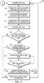
- FIG. 12 illustrates a method 800 of enlarging the power transfer area of a wireless power transfer device 105. As shown in FIG. 12 , the method 800 includes overlapping a first portion 150 of the first coil 115 with a second portion 165 of the second coil 120 to form an overlap region 170 (block 805). The method 800 also includes aligning the flux concentrator 195 with the overlap region 170 (block 810). As shown in FIG. 2B , the flux concentrator 195 is positioned below the second coil 120 in the illustrated embodiment. A power amplifier 130 is then used to generate a drive signal (block 815).
- the first coil 115 or the second coil 120 receives the drive signal from the power amplifier 130 (block 820), and in response to receiving the drive signal, the first coil 115 or the second coil 120 generate a magnetic field (block 825).
- both the first coil 115 and the second coil 120 are tuned, both the first coil 115 and the second coil 120 generate a magnetic field and transfer power.
- the power transfer efficiency provided by the overlapping first coil 115 and second coil 120 is higher than the power transfer efficiency provided by an enlarged transmitter coil including an impedance matching circuit (e.g., simply an expanded first coil 115 coupled to an impedance matching circuitry).
- the wireless power transfer device 105 including the partially overlapping first coil 115 and second coil 120 and using the switch network 125 to detune one of the first coil 115 or second coil 120 provides a power transfer efficiency of approximately 70%, without utilizing an impedance matching circuit.
- relational terms such as first and second, top and bottom, and the like may be used solely to distinguish one entity or action from another entity or action without necessarily requiring or implying any actual such relationship or order between such entities or actions.
- processors such as microprocessors, digital signal processors, customized processors and field programmable gate arrays (FPGAs) and unique stored program instructions (including both software and firmware) that control the one or more processors to implement, in conjunction with certain non-processor circuits, some, most, or all of the functions of the method and/or apparatus described herein.
- processors or “processing devices”
- FPGAs field programmable gate arrays
- unique stored program instructions including both software and firmware
- an embodiment can be implemented as a computer-readable storage medium having computer readable code stored thereon for programming a computer (e.g., comprising a processor) to perform a method as described and claimed herein.
- Examples of such computer-readable storage mediums include, but are not limited to, a hard disk, a CD-ROM, an optical storage device, a magnetic storage device, a ROM (Read Only Memory), a PROM (Programmable Read Only Memory), an EPROM (Erasable Programmable Read Only Memory), an EEPROM (Electrically Erasable Programmable Read Only Memory) and a Flash memory.
Landscapes
- Engineering & Computer Science (AREA)
- Power Engineering (AREA)
- Computer Networks & Wireless Communication (AREA)
- Signal Processing (AREA)
- Charge And Discharge Circuits For Batteries Or The Like (AREA)
- Near-Field Transmission Systems (AREA)
Description
- Interest for wireless power transfer has been growing recently. Additionally, there are various applications for wireless power transfer such as, for example, charging of batteries in small electronic devices (e.g., smart telephones, tablet computers, and the like), electric vehicles, and/or other electronic devices. Wireless power transfer (WPT) may be achieved in a number of ways. One wireless power transfer technology is magnetic-resonance power transfer.
-
WO2015/175096A1 (Qualcomm Incorporated) provides a structure that comprises two coils. The coils and an accompanying ferromagnetic layer are designed to have a low overall height. The ferromagnetic layer provides a large area underneath all of both coils, and may be constructed of tiles. At least one portion of the ferromagnetic layer has a reduced thickness, and provides a recess in the ferromagnetic layer. A first coil has at least one portion countersunk into the portion of the ferromagnetic layer that has the reduced thickness. A second coil overlaps the at least one countersunk portion of the first coil. The structure ofWO2015/175096A1 is designed to charge a vehicle that is to be parked above the coils. When a vehicle is parked above the coils, that vehicle may not be in optimal alignment with the coils. This situation is described inWO2015/175096A1 as the vehicle being 'moved slightly' in one or both of the directions that are parallel and/or perpendicular to a common axis of the first and second coils. In order to address instances where the vehicle is not aligned with the common axis of the first and second coils,WO2015/175096A1 proposes a particular shape of the coils. A receive coil of the vehicle may be misaligned with the common axis of the first and second coils by a certain distance, which is referred to inWO2015/175096A1 as an 'offset distance'.WO2015/175096A1 proposes to elongate the shape of the parts of the first and second coils where the second coil overlaps the at least one countersunk portion of the first coil. The elongation of the coils is in a direction that is perpendicular to the common axis of the coils. The extent of the elongation of the coils is much greater than the offset distance by which the receive coil of the vehicle may be misaligned with the common axis of the first and second coils, seefigure 8 ofWO2015/175096A1 .WO2015/175096A1 chooses to substantially increase one physical dimension of the overlap region of the coils, in order to address the problem of a vehicle that is misaligned by a comparatively much smaller offset distance.WO2015/175096A1 is choosing a structural solution, i.e. a particular design geometry that involves the shapes of both coils being substantially elongated. - The accompanying figures, where like reference numerals refer to identical or functionally similar elements throughout the separate views, together with the detailed description below, are incorporated in and form part of the specification, and serve to further illustrate embodiments of concepts that include the claimed invention, and explain various principles and advantages of those embodiments.
-
FIG. 1 is a block diagram of a wireless power transfer system. -
FIGS. 2A through 2B are diagrams of a wireless power transfer device of the wireless power transfer system ofFIG. 1 . -
FIGS. 3A through 3D are diagrams of different configurations of a transmitter coil and a repeater coil of the wireless power transfer device ofFIGS. 2A through 2B . -
FIGS. 4A through 4D are diagrams illustrating different configurations of a switch network of the wireless power transfer device ofFIGS. 2A through 2B . -
FIGS. 5A through 5D are diagrams illustrating different positions of a receiver coil with respect to the wireless power transfer device ofFIGS. 2A through B . -
FIG. 6 is a flowchart illustrating a method of determining a configuration for the switch network based on a position of a receiver coil. -
FIG. 7 is a graph illustrating an exemplary power transfer efficiency when a single receiver coil is coupled to the wireless power transfer device ofFIGS. 2A through 2B and the wireless power transfer device does not detune a first coil of the wireless power transfer device. -
FIG. 8 is a flowchart illustrating the overall operation of the wireless power transfer device ofFIGS. 2A through 2B . -
FIGS. 9A and9B together are a flowchart illustrating a method of tracking the receiver coil when the receiver coil is positioned closest to an overlap region of the wireless power transfer device ofFIGS. 2A through 2B . -
FIG. 10 is a flowchart illustrating a method of tracking the receiver coil when the receiver coil is positioned closest to a first coil of the wireless power transfer device ofFIGS. 2A through B . -
FIG. 11 is a flowchart illustrating a method of tracking the receiver coil when the receiver coil is positioned closest to a second coil of the wireless power transfer device ofFIGS. 2A through B . -
FIG. 12 is a flowchart illustrating a method of enlarging a power transfer area of a wireless power transfer device. - Skilled artisans will appreciate that elements in the figures are illustrated for simplicity and clarity and have not necessarily been drawn to scale. For example, the dimensions of some of the elements in the figures may be exaggerated relative to other elements to help to improve understanding of embodiments of the present invention.
- The apparatus and method components have been represented where appropriate by conventional symbols in the drawings, showing only those specific details that are pertinent to understanding the embodiments of the present invention so as not to obscure the disclosure with details that will be readily apparent to those of ordinary skill in the art having the benefit of the description herein.
- One embodiment provides a wireless power transfer device that in one particular instance includes a first coil having a first portion. The first coil is configured to generate a magnetic field. The wireless power transfer device also includes a second coil having a second portion. The second coil is positioned with respect to the first coil such that the first portion of the first coil overlaps the second portion of the second coil in an overlap region. The wireless power transfer device also includes a power amplifier electrically coupled to one selected from a group consisting of the first coil and the second coil, and configured to output a drive signal. The wireless power transfer device further includes a flux concentrator aligned with the overlap region and configured to concentrate a magnetic flux of the magnetic field. Details of the embodiment of the wireless power transfer device are provided in appended independent claim 1.
- Another embodiment provides a method of wirelessly transferring power with a wireless power transfer device that includes a first coil, a second coil, a power amplifier, a switch network, and an electronic processor. In one instance, the method includes overlapping a first portion of the first coil with a second portion of the second coil in an overlap region, aligning a flux concentrator with the overlap region, and generating, with the power amplifier, a drive signal. The method further includes receiving the drive signal by one selected from a group consisting of the first coil and the second coil, and generating, by one selected from the group consisting of the first coil and the second coil, a magnetic field in response to receiving the drive signal. Details of the embodiment of the method of wirelessly transferring power are provided in appended independent claim 14.
-
FIG. 1 illustrates a wirelesspower transfer system 100 including a wirelesspower transfer device 105 and anexternal device 110. In the example illustrated, theexternal device 110 includes, among other things, areceiver coil 113. Thereceiver coil 113 magnetically couples to the wirelesspower transfer device 105 to receive electrical power from the wirelesspower transfer device 105. Theexternal device 110 may be, for example, a battery. The battery may be located in a smart telephone, a tablet computer, or other electrical device. For the sake of simplicity, the particular components of theexternal device 110 are not shown, but are understood by one of skill in the art. - In the embodiment illustrated, the wireless
power transfer device 105 transfers power wirelessly to theexternal device 110 through magnetic resonance. In magnetic-resonance power transfer, a transmitter coil (i.e., the coil transmitting power) receives a current from, for example, a power amplifier, and generates a magnetic field. A receiver coil (i.e., the coil receiving power), for example, thereceiver coil 113, is placed in close proximity to the transmitter coil. Power is transferred as a consequence of the receiver coil magnetically coupling to the transmitter coil. The efficiency of the power transfer is improved when the transmitter coil and the receiver coil have the same or similar size and form factor. However, in many applications it is not possible to match the size and form of the transmitter and receiver coils. For example, a wireless battery charger may be designed to charge batteries having a receiver coil of a certain configuration, but batteries may be manufactured by many different entities and lack a uniform configuration. As shown inFIG. 1 , the wirelesspower transfer device 105 includes afirst coil 115, asecond coil 120, aswitch network 125, apower amplifier 130, and anelectronic processor 135. The wirelesspower transfer device 105 also includes a housing (not shown) that supports thefirst coil 115, thesecond coil 120, theswitch network 125, thepower amplifier 130, and theelectronic processor 135. In some embodiments, the wirelesspower transfer device 105 may include more or less components than those mentioned above. - As shown in
FIG. 2A , thefirst coil 115 includes a first looped wire having a firstpositive terminal 116 and a firstnegative terminal 118. Thesecond coil 120 includes a second looped wire having a secondpositive terminal 122 and a secondnegative terminal 124. As shown inFIG. 1 , thefirst coil 115 and thesecond coil 120 are coupled to theswitch network 125, and are configured to selectively and, in some cases, simultaneously, receive power from thepower amplifier 130 according to a configuration of theswitch network 125. Thepower amplifier 130 generates a drive signal that is provided to thefirst coil 115, thesecond coil 120, or both. Thefirst coil 115 and thesecond coil 120 generate a magnetic field in response to receiving the drive signal from thepower amplifier 130. When thereceiver coil 113 is within an applicable transmission range, thereceiver coil 113 is magnetically coupled to the magnetic field generated by thefirst coil 115, thesecond coil 120, or both. As a consequence, electrical power is transferred from the wirelesspower transfer device 105 to thereceiver coil 113. - In one particular embodiment, as shown in
FIG. 2B , thefirst coil 115 has afirst length 140 of, for example, approximately eighteen (18) centimeters (cm) and afirst width 145 of, for example, approximately twelve (12) centimeters. It should be understood; however, that these dimensions (as well as other dimensions provided herein) are examples and different dimensions could be used. Thefirst coil 115 also includes a first portion 150 located at a firstlongitudinal end 152 of thefirst coil 115 along thefirst width 145. In the illustrated embodiment, thesecond coil 120 is substantially similar to thefirst coil 115. Thus, thesecond coil 120 has asecond length 155 of approximately eighteen centimeters and asecond width 160 of approximately twelve centimeters. Thesecond coil 120 also includes asecond portion 165 located at a secondlongitudinal end 147 of thesecond coil 120 along thesecond width 160. As shown inFIG. 2B , thesecond coil 120 is positioned such that the first portion 150 of thefirst coil 115 overlaps thesecond portion 165 of thesecond coil 120 in anoverlap region 170. As shown inFIG. 2B , the size of theoverlap region 170 is smaller than the size of thefirst coil 115 and smaller than the size of thesecond coil 120. In other words, thefirst coil 115 and thesecond coil 120 are only partially overlapped. The size (e.g., area and dimensions) of theoverlap region 170 is not arbitrary, and is determined based on, for example, a geometry of thefirst coil 115, a geometry of thesecond coil 120, a number of turns of thefirst coil 115, a number of turns of thesecond coil 120, a width of turns of thefirst coil 115, a width of turns of thesecond coil 120, a spacing between the turns of thefirst coil 115, a spacing between the turns of thesecond coil 120, among other things. In the illustrated embodiment, theoverlap region 170 has athird length 175 of approximately two (2) centimeters and athird width 180 of approximately twelve centimeters. In other words, the first portion 150 overlaps thesecond portion 165 by approximately two centimeters. Therefore, the overlappedfirst coil 115 andsecond coil 120 have anaggregate length 185 of approximately thirty-four (34) centimeters and anaggregate width 190 of approximately twelve centimeters. In other embodiments, theoverlap region 170 may have different dimensions based on particular dimensions of thefirst coil 115 and thesecond coil 120. - As shown in
FIG. 2B , the wirelesspower transfer device 105 also includes aflux concentrator 195 that concentrates the magnetic flux between thefirst coil 115 and thesecond coil 120. In other words, theflux concentrator 195 maximizes the magnetic flux coupling between thefirst coil 115 and thesecond coil 120 while minimizing magnetic losses in the coupling. In the embodiment illustrated, theflux concentrator 195 is aligned with theoverlap region 170 and positioned underneath thesecond coil 120, as shown inFIG. 2B . In this position, theflux concentrator 195, due to its material properties, can improve the return loss when thefirst coil 115 and thesecond coil 120 are magnetically coupled. In the illustrated embodiment, theflux concentrator 195 includes a ferrite layer. Theflux concentrator 195 also has a high permeability (e.g., 120) and low-loss factor (e.g., 0.017). In the illustrated embodiment, theflux concentrator 195 has afirst height 200 of approximately three tenths of a millimeter (0.3 mm). Additionally, as shown inFIG. 2B , spacers 205a, 205b separate thefirst coil 115 from thesecond coil 120, and thesecond coil 120 from theflux concentrator 195. Thespacers 205a, 205b include a passive material and are used to keep thefirst coil 115 and thesecond coil 120 anappropriate distance 207 apart. In one embodiment, thespacers 205a, 205b include an insulating material having asecond height 210 of approximately 2 mm. In the illustrated embodiment, thespacers 205a, 205b use a microcellular urethane material by the name of PORON ®. In other embodiments, thespacers 205a, 205b may use other type of insulating material. Thedistance 207 between thefirst coil 115 and thesecond coil 120 is not arbitrary, and is determined based on, for example, the geometry of thefirst coil 115, the geometry of thesecond coil 120, the number of turns in thefirst coil 115, the number of turns in the second coil120, and the like. -
FIG. 3A shows the configuration of theoverlap region 170 as described above with respect toFIGS. 2A and2B . However, theoverlap region 170 may be shaped and sized differently than the size and shape shown inFIGS. 2A and2B .FIGS. 3B through 3D illustrate variations of theoverlap region 170 and configurations of the first portion 150 of thefirst coil 115 and thesecond portion 165 of thesecond coil 120. -
FIG. 3B shows the first portion 150 of thefirst coil 115 located along thefirst length 140 of thefirst coil 115, and thesecond portion 165 of thesecond coil 120 located along thesecond length 155 of thesecond coil 120. Therefore, theoverlap region 170 shown inFIG. 3B is positioned along thefirst length 140 of thefirst coil 115 and thesecond length 155 of thesecond coil 120. - In contrast,
FIG. 3C illustrates the first portion 150 of thefirst coil 115 positioned along thefirst width 145 of thefirst coil 115, and thesecond portion 165 of thesecond coil 120 located along thesecond length 155 of thesecond coil 120. InFIG. 3C , theoverlap region 170 is positioned along thefirst width 145 of thefirst coil 115, and along thesecond length 155 of thesecond coil 120, thereby forming an L shapedoverlap region 170. -
FIG. 3D illustrates the first portion 150 of thefirst coil 115 positioned along thefirst length 140 of thefirst coil 115, and thesecond portion 165 of thesecond coil 120 positioned along thesecond width 160 of thesecond coil 120. InFIG. 3D , theoverlap region 170 is positioned along thefirst length 140, and along thesecond width 160, thereby forming a T shapedoverlap region 170. Variations beyond those shown inFIGS. 3A through 3D are possible. For example, thefirst coil 115 as shown inFIG. 3C can be positioned centrally with respect to thesecond coil 120 such that a sideways T shape is formed instead of an L shape. - In some applications, it may be desired to enlarge a power transfer area of the wireless
power transfer device 105 to, for example, provide greater flexibility on where to place theexternal device 110 for power transfer and/or provide the ability to transfer power to multiple external devices. Typically, the power transfer area is enlarged by expanding the size of a transmitter coil (i.e., the coil transmitting power from the wireless power transfer device 105). However, enlarging the power transfer area by expanding the size of a transmitter coil may lead to a mismatch of the size and form factor of the transmitter coil and thereceiver coil 113 of theexternal device 110. The wirelesspower transfer device 105 shown inFIG. 1 , however, uses thefirst coil 115, thesecond coil 120, and theswitch network 125 to effectively enlarge the power transfer area of the wirelesspower transfer device 105 while minimizing the effects of a mismatch of the size or the form factor between a transmitter coil of the wireless power transfer device 105 (e.g., thefirst coil 115 or the second coil 120). - As noted above with respect to
FIG. 1 , thefirst coil 115 and thesecond coil 120 are electrically coupled to theswitch network 125 and theswitch network 125 is electrically coupled to thepower amplifier 130.FIGS. 4A through 4D illustrate various configurations of theswitch network 125. Theswitch network 125 includes a plurality of switches to selectively detune thefirst coil 115, thesecond coil 120, or neither. As shown inFIGS. 4A through 4D , theswitch network 125 includes afirst power switch 300, asecond power switch 305, afirst detuning component 310, asecond detuning component 315, afirst detuning switch 320, and asecond detuning switch 325. In some embodiments, theswitch network 125 may include more or less switches and/or detuning components. For example, in some embodiments, the wirelesspower transfer device 105 may include more than two coils (e.g., a third coil), in which case theswitch network 125 may also include additional switches and detuning components than the ones shown inFIGS. 4A through 4D . - The
first power switch 300 selectively electrically couples thefirst coil 115 to thepower amplifier 130. Thesecond power switch 305 selectively electrically couples thesecond coil 120 to thepower amplifier 130. Thefirst power switch 300 and thesecond power switch 305 are each switchable between a conducting state, in which thepower amplifier 130 is electrically coupled to thefirst coil 115, and thesecond coil 120, respectively, and a non-conducting state, in which thepower amplifier 130 is electrically decoupled (e.g., disconnected) from thefirst coil 115, and thesecond coil 120, respectively. - The
first detuning component 310 is selectively electrically coupled to thefirst coil 115 through thefirst detuning switch 320. Thefirst detuning switch 320 is switchable between a conducting state in which thefirst coil 115 is electrically coupled to thefirst detuning component 310, and a non-conducting state in which thefirst coil 115 is decoupled (e.g., disconnected) from thefirst detuning component 310. When thefirst detuning component 310 is electrically coupled to the first coil 115 (i.e., when thefirst detuning switch 320 is in the conducting state), thefirst detuning component 310 changes the resonant frequency of thefirst coil 115, which decreases the operability of thefirst coil 115 to transfer power to theexternal device 110. Therefore, when thefirst detuning component 310 is coupled to thefirst coil 115, thefirst detuning component 310 detunes thefirst coil 115. In some embodiments, thefirst detuning component 310 may change another characteristic of thefirst coil 115 and/or the magnetic field generated by thefirst coil 115 that decreases the operability of thefirst coil 115 to transfer power. In the illustrated embodiment, thefirst detuning component 310 includes a detuning capacitor. In other embodiments, other electrical components may be used that, when electrically coupled to thefirst coil 115, detune thefirst coil 115. - The
second detuning component 315 is selectively electrically coupled to thesecond coil 120 through thesecond detuning switch 325. Thesecond detuning switch 325 is switchable between a conducting state in which thesecond coil 120 is electrically coupled to thesecond detuning component 315, and a non-conducting state in which thesecond coil 120 is decoupled (e.g., disconnected) from thesecond detuning component 315. When thesecond detuning component 315 is electrically coupled to the second coil 120 (i.e., when thesecond detuning switch 325 is in the conducting state), thesecond detuning component 315 changes the resonant frequency of thesecond coil 120, or changes another characteristic of thesecond coil 120 and/or the magnetic field generated by thesecond coil 120 such that the operability of the second coil to transfer power is decreased. Therefore, when thesecond detuning component 315 is coupled to thesecond coil 20, thesecond detuning component 315 detunes thesecond coil 120. In the illustrated embodiment, thesecond detuning component 315 includes a detuning capacitor. Components other than a capacitor may be used to detune thesecond coil 120. - Based on a state of the first and second power switches 300 and 305 and the first and second detuning switches 320 and 325, the
switch network 125 selectively connects thepower amplifier 130 to one of thefirst coil 115, or thesecond coil 120. As shown inFIGS. 4A through 4D , theswitch network 125 can be placed in four different configurations.FIG. 4A illustrates afirst configuration 327 of theswitch network 125 in which thefirst power switch 300 is in the conducting state, thefirst detuning switch 320 is in the non-conducting state, thesecond power switch 305 is in the non-conducting state, and thesecond detuning switch 325 is in the conducting state. In thefirst configuration 327, thepower amplifier 130 is electrically coupled to thefirst coil 115 while thesecond coil 120 is detuned via thesecond detuning component 315. Therefore, thepower amplifier 130 provides the drive signal to thefirst coil 115, and only thefirst coil 115 generates a magnetic field to transfer power to thereceiver coil 113 of theexternal device 110. In thefirst configuration 327, thefirst coil 115 is the transmitter coil (i.e., the coil receiving a drive signal from the power amplifier and, in response to the drive signal, generating the magnetic field to transfer power to the receiver coil 113) of the wirelesspower transfer device 105. -
FIG. 4B illustrates asecond configuration 329 of theswitch network 125 in which thefirst power switch 300 and thesecond detuning switch 325 are in the non-conducting state, and thefirst detuning switch 320 and thesecond power switch 305 are in the conducting state. In thesecond configuration 329, thepower amplifier 130 is electrically coupled to thesecond coil 120 while thefirst coil 115 is detuned via thefirst detuning component 310. Therefore, thepower amplifier 130 provides the drive signal to thesecond coil 120, and only thesecond coil 120 generates a magnetic field to transfer power to thereceiver coil 113 of theexternal device 110. In thesecond configuration 329, thesecond coil 120 is the transmitter coil (i.e., the coil receiving a drive signal from the power amplifier and, in response to the drive signal, generating the magnetic field to transfer power to the receiver coil 113) of the wirelesspower transfer device 105. When theswitch network 125 is in thefirst configuration 327 or thesecond configuration 329, only one of the coils (e.g., thefirst coil 115 or the second coil 120) generates a magnetic field and transfers power to the external device 110 (e.g., is the transmitter coil). Therefore, when theswitch network 125 operates in either thefirst configuration 327 or thesecond configuration 329, theswitch network 125 is said to operate in an individual configuration in which either thefirst coil 115 or thesecond coil 120 is detuned. -
FIG. 4C illustrates athird configuration 331 of theswitch network 125 in which thefirst power switch 300 is in the conducting state, while thesecond power switch 305, thefirst detuning switch 320, and thesecond detuning switch 325 are in the non-conducting state. In thethird configuration 331, thepower amplifier 130 is electrically coupled to thefirst coil 115 and provides the drive signal to thefirst coil 115, which in response to receiving the drive signal, generates a first magnetic field. Thesecond coil 120, since it is magnetically coupled to thefirst coil 115 and decoupled from thesecond detuning component 315, generates a second magnetic field in response to thefirst coil 115 generating the first magnetic field. While theswitch network 125 is in thethird configuration 331, both thefirst coil 115 and thesecond coil 120 transfer power to theexternal device 110, even though only thefirst coil 115 receives the drive signal from thepower amplifier 130. In other words, while theswitch network 125 is in the third configuration, thefirst coil 115 behaves as a transmitter coil (e.g., because thefirst coil 115 receives the drive signal from thepower amplifier 130 and, in response, generates a first magnetic field), while thesecond coil 120 behaves as a repeater coil (i.e., a coil that is magnetically coupled to a transmitter coil and that generates a magnetic field in response to the transmitter coil generating a magnetic field). -
FIG. 4D illustrates afourth configuration 333 of theswitch network 125 in which thesecond power switch 305 is in the conducting state while thefirst power switch 300, thefirst detuning switch 320, and thesecond detuning switch 325 are in the non-conducting state. In thefourth configuration 333, thepower amplifier 130 is electrically coupled to thesecond coil 120 and provides the drive signal to thesecond coil 120, which generates a magnetic field in response to receiving the drive signal. Thefirst coil 115, since it is magnetically coupled to thesecond coil 120 and decoupled from thefirst detuning component 310, generates another magnetic field in response to thesecond coil 120 generating the magnetic field. Therefore, while theswitch network 125 is in thefourth configuration 333, both thefirst coil 115 and thesecond coil 120 transfer power to theexternal device 110, even though only thesecond coil 120 receives the drive signal from thepower amplifier 130. In other words, while theswitch network 125 is in thefourth configuration 333, thesecond coil 120 behaves as a transmitter coil (e.g., because thesecond coil 120 receives the drive signal from thepower amplifier 130 and, in response, generates a magnetic field), while thefirst coil 115 behaves as a repeater coil (i.e., because thefirst coil 115 is magnetically coupled to a transmitter coil (e.g., the second coil 120) and generates a magnetic field in response to the transmitter coil generating a magnetic field). When theswitch network 125 operates in thethird configuration 331 or thefourth configuration 333 both thefirst coil 115 and thesecond coil 120 generate a magnetic field, and both thefirst coil 115 and thesecond coil 120 can perform a power transfer operation (i.e., transfer power to the external device 110). Therefore, when theswitch network 125 operates in either thethird configuration 331 or thefourth configuration 333, theswitch network 125 is said to operate in a combined configuration in which both thefirst coil 115 and thesecond coil 120 are tuned and can transfer power to theexternal device 110. - As shown in
FIG. 1 , theswitch network 125 is electrically coupled to theelectronic processor 135. Theelectronic processor 135 controls the state of each of theswitches switch network 125. In the illustrated embodiment, theelectronic processor 135 determines which configuration to place theswitch network 125 in based on a position of thereceiver coil 113. As shown inFIGS. 5A through 5D , one or more receiver coils 113 can be coupled to the wirelesspower transfer device 105.FIG. 5A shows asingle receiver coil 113 positioned closest to thefirst coil 115.FIG. 5B shows asingle receiver coil 113 positioned closest to thesecond coil 120.FIG. 5C shows asingle receiver coil 113 positioned closest to theoverlap region 170.FIG. 5D shows a first receiver coil 113a positioned closest to thefirst coil 115 and a second receiver coil 113b positioned closest to thesecond coil 120. Thereceiver coil 113, the first receiver coil 113a, or the second receiver coil 113b are positioned "closest" to thefirst coil 115, thesecond coil 120, or theoverlap region 170 relative to other positions of thereceiver coil 113, thefirst receiver coil 113, or the second receiver coil 113b with respect to the wirelesspower transfer device 105. In other words, areceiver coil 113 may be positioned anywhere on a surface of the wirelesspower transfer device 105. While thereceiver coil 113 remains on the surface of the wirelesspower transfer device 105, thereceiver coil 113 may be positioned closer to, for example, thefirst coil 115, relative to thesecond coil 120 and relative to theoverlap region 170. - When a
single receiver coil 113 is positioned closest to thefirst coil 115, as shown inFIG. 5A , and theswitch network 125 is in a combined configuration (i.e., both thefirst coil 115 and thesecond coil 120 transfer power), the power transferred by thesecond coil 120 remains unused because there is no external device positioned to receive the power from thesecond coil 120. Accordingly, the overall efficiency at which power is transferred from the wirelesspower transfer device 105 decreases when both thefirst coil 115 and thesecond coil 120 generate a magnetic field, but thereceiver coil 113 is positioned to receive wireless power from only thefirst coil 115. To reduce the loss of power and increase the power transfer efficiency in such situations, theelectronic processor 135 detects that only onereceiver coil 113 is coupled to the wirelesspower transfer device 105, detects the position of thereceiver coil 113, and places theswitch network 125 in the appropriate individual configuration based on whether thereceiver coil 113 is positioned closest to thefirst coil 115 or thesecond coil 120. Analogously, when two receiver coils 113a and 113b are coupled to the wirelesspower transfer device 105, as shown for example inFIG. 5D , but only thefirst coil 115 or thesecond coil 120 generates a magnetic field to transfer power, the overall power transfer efficiency also decreases. Therefore, theelectronic processor 135 places theswitch network 125 in a combined configuration when multiple receiver coils 113a, 113b (FIG. 5D ) are coupled to the wirelesspower transfer device 105, thereby increasing the power transfer efficiency. - The
electronic processor 135 determines the position of thereceiver coil 113 based on a first impedance associated with thefirst coil 115 and on a second impedance associated with thesecond coil 120. The impedance associated with thefirst coil 115 and the impedance associated with thesecond coil 120 refer to the apparent opposition in an electrical circuit to the flow of current. When thereceiver coil 113 approaches the first coil 115 (e.g., thereceiver coil 113 magnetically couples to thefirst coil 115 because theexternal device 110 is placed closest to thefirst coil 115 relative to thesecond coil 120 and theoverlap region 170, as shown inFIG. 5A ), the first impedance associated with thefirst coil 115 decreases. Similarly, when thereceiver coil 113 approaches the second coil 120 (e.g., thereceiver coil 113 magnetically couples to thesecond coil 120 because theexternal device 110 is placed closest to thesecond coil 120 relative to thefirst coil 115 and theoverlap region 170, as shown inFIG. 5B ), the second impedance associated with thesecond coil 120 decreases. Theelectronic processor 135 monitors changes in the first impedance associated with thefirst coil 115 and the second impedance associated with thesecond coil 120. Detecting a change in the first impedance associated with thefirst coil 115 and/or the second impedance associated with thesecond coil 120 serves as an indication to theelectronic processor 135 of the relative position of thereceiver coil 113. After theelectronic processor 135 determines the position of thereceiver coil 113, theelectronic processor 135 controls the switch network 125 (i.e., controls the plurality of switches of the switch network 125) to place theswitch network 125 in thefirst configuration 327, thesecond configuration 329, thethird configuration 331, or thefourth configuration 333. - In the illustrated embodiment, when the
electronic processor 135 determines that thereceiver coil 113 is positioned closest to thefirst coil 115 relative to thesecond coil 120 and the overlap region 170 (FIG. 5A ), theelectronic processor 135 places theswitch network 125 in the first configuration 327 (shown inFIG. 4A ). When theelectronic processor 135 determines that thereceiver coil 113 is positioned closest to thesecond coil 120 relative to thefirst coil 115 and theoverlap region 170, as shown inFIG. 5B , theelectronic processor 135 places theswitch network 125 in the second configuration 329 (shown inFIG. 4B ). When theelectronic processor 135 determines that thereceiver coil 113 is positioned closest to theoverlap region 170 relative to thefirst coil 115 and the second coil 120 (as shown inFIG. 5C ), or that multiple receiver coils 113a, 113b are coupled to the wireless power transfer device 105 (as shown inFIG. 5D ), theelectronic processor 135 places theswitch network 125 in either thethird configuration 331 or thefourth configuration 333. -
FIG. 6 illustrates anexemplary method 340 implemented by theelectronic processor 135 to determine the configuration for theswitch network 125 based on a position of the receiver coil 113 (e.g., whether thereceiver coil 113 is positioned closest to thefirst coil 115, thesecond coil 120, or the overlap region 170). As shown inFIG. 6 , theelectronic processor 135 monitors a parameter of thefirst coil 115 and thesecond coil 120. As discussed above, in the embodiment illustrated inFIGS. 1 through 6 , theelectronic processor 135 monitors the first impedance associated with thefirst coil 115 and the second impedance associated with thesecond coil 120. In some embodiments, theelectronic processor 135 may, additionally or alternatively, monitor other parameters associated with thefirst coil 115 andsecond coil 120 that help determine the relative position of thereceiver coil 113. As shown inFIG. 6 , theelectronic processor 135 periodically activates (e.g., by providing the drive signal from the power amplifier 130) thefirst coil 115 and/or the second coil 120 (block 345). Periodically powering thefirst coil 115 and thesecond coil 120 allows theelectronic processor 135 to detect changes in the first impedance associated with thefirst coil 115 and the second impedance associated with thesecond coil 120. Theelectronic processor 135 monitors the first impedance associated with thefirst coil 115 and determines whether a first impedance change indicative of a decrease in the first impedance of thefirst coil 115 is detected by the electronic processor 135 (block 350). When theelectronic processor 135 detects a change in the first impedance associated with the first coil 115 (e.g., a monitored parameter), theelectronic processor 135 then determines whether a second impedance change indicative of a decrease in the second impedance associated with thesecond coil 120 is also detected (block 355). If theelectronic processor 135 detects the second impedance change at block 355 (i.e., detects both the first impedance change and the second impedance change), theelectronic processor 135 activates both thefirst coil 115 and the second coil 120 (block 360) by placing theswitch network 125 in a combined configuration (i.e., in either thethird configuration 331 or the fourth configuration 333). Theelectronic processor 135 may detect a first impedance change and a second impedance change when thereceiver coil 113 is positioned closest to the overlap region 170 (as shown inFIG. 5C ), or when a first receiver coil 113a is positioned closest to thefirst coil 115 and a second receiver coil 113b is positioned closest to the second coil 120 (as shown inFIG. 5D ). Referring back to block 355, if the second impedance change is not detected (i.e., processor detects only the first impedance change), theelectronic processor 135 activates only thefirst coil 115 to transfer power (block 365) by placing theswitch network 125 in thefirst configuration 327. Theelectronic processor 135 may detect the first impedance change, but not the second impedance change when thereceiver coil 113 is positioned closest to thefirst coil 115 relative to thesecond coil 120 and theoverlap region 170. - With reference to block 350, if the first impedance change is not detected (i.e., the
electronic processor 135 does not detect the first impedance change), theelectronic processor 135 determines whether a second impedance change indicative of a decrease in the second impedance of thesecond coil 120 is detected (block 370). If theelectronic processor 135 detects the second impedance change (i.e., only detects the second impedance change, but not the first impedance change), theelectronic processor 135 activates only thesecond coil 120 for power transfer (block 375) by placing theswitch network 125 in thesecond configuration 329. Theelectronic processor 135 may detect the second impedance change, but not the first impedance change when thereceiver coil 113 is positioned closest to thesecond coil 120 relative to thefirst coil 115 and theoverlap region 170. If, however, the second impedance change is not detected at block 370 (i.e., theelectronic processor 135 does not detect the first impedance change or the second impedance change), theelectronic processor 135 returns to block 345 to periodically activate thefirst coil 115 and thesecond coil 120 and thereby continue to monitor the first impedance associated with thefirst coil 115 and the second impedance associated with thesecond coil 120 for detection of an approachingreceiver coil 113. - By controlling the
switch network 125 based on a detected position of thereceiver coil 113 determined at least in part by a monitored parameter of a power transfer operation (e.g., first impedance associated with thefirst coil 115 or second impedance associated with the second coil 120), the wirelesspower transfer device 105 may effectively change the size of the wireless power transfer area to maximize the power transfer efficiency. In other words, and as discussed above, the wirelesspower transfer device 105 can activate a smaller wireless power transfer area (e.g., by activating only thefirst coil 115 or the second coil 120) when asingle receiver coil 113 is coupled to the wirelesspower transfer device 105, and can activate an enlarged power transfer area (e.g., by activating both thefirst coil 115 and the second coil 120) when, for example, multiple receiver coils 113a, 113b are coupled to the wirelesspower transfer device 105. - Additionally, detuning the
first coil 115 or thesecond coil 120 when only asingle receiver coil 113 is coupled to the wirelesspower transfer device 105 also increases the power transfer efficiency of the wirelesspower transfer device 105 when performing a power transfer operation.FIG. 7 illustrates a graph showing one example of the power transfer efficiency (e.g., a monitored efficiency) when asingle receiver coil 113 is coupled to the wirelesspower transfer device 105 as shown inFIG. 5B , and the wirelesspower transfer device 105 does not detune thefirst coil 115. As shown on the graph, the power transfer efficiency is approximately equal to sixty percent (60%). However, when thesingle receiver coil 113 is coupled to the wirelesspower transfer device 105 as shown inFIG. 5B again and theswitch network 125 detunes thefirst coil 115, the power transfer efficiency increases to approximately seventy percent (70%). Therefore, by detuning thefirst coil 115 or thesecond coil 120, whichever is farthest from thereceiver coil 113, the wirelesspower transfer device 105 can achieve a greater power transfer efficiency. - To maintain an increased power transfer efficiency, the
electronic processor 135 continues to track the position of theexternal device 110 even after theelectronic processor 135 detects the initial position of the receiver coil 113 (as shown inFIG. 6 ) and after power transfer has initiated.FIG. 8 is a flowchart illustrating the overall operation of the wirelesspower transfer device 105. Theelectronic processor 135 monitors the first impedance associated with thefirst coil 115 and second impedance associated with the second coil 120 (block 400). Theelectronic processor 135 determines whether areceiver coil 113 is coupled to the wirelesspower transfer device 105 based on the monitored impedance (block 405). While theelectronic processor 135 does not detect that areceiver coil 113 has coupled to the wirelesspower transfer device 105, theelectronic processor 135 continues to monitor the first impedance associated with thefirst coil 115 and the second impedance associated with the second coil 120 (block 400). As discussed above, theelectronic processor 135 monitors the first impedance associated with thefirst coil 115 and the second impedance associated with thesecond coil 120 by periodically and selectively activating thefirst coil 115 and thesecond coil 120. When, on the other hand, theelectronic processor 135 detects that areceiver coil 113 has coupled to the wirelesspower transfer device 105, theelectronic processor 135 determines the location of thereceiver coil 113 at block 410 (i.e., determines whether thereceiver coil 113 is positioned closest to thefirst coil 115, thesecond coil 120, or the overlap region 170). As discussed above, theelectronic processor 135 determines the location of thereceiver coil 113 based on the detected first impedance associated with thefirst coil 115 and second impedance associated with thesecond coil 120. Thereby, theelectronic processor 135 determines whether thereceiver coil 113 is placed nearest thefirst coil 115, nearest thesecond coil 120, nearest theoverlap region 170, and/or if multiple receiver coils 113a, 113b are coupled to the wirelesspower transfer device 105. - Once the
electronic processor 135 determines the location of thereceiver coil 113, theelectronic processor 135 places theswitch network 125 in the appropriate configuration corresponding to the determined location of the receiver coil 113 (block 415). The wirelesspower transfer device 105 begins power transfer to the receiver coil 113 (block 420). While the wirelesspower transfer device 105 is transferring power to thereceiver coil 113, theelectronic processor 135 monitors the power transfer efficiency (e.g., an efficiency parameter of a power transfer operation) atblock 425. Based on the power transfer efficiency (e.g., a monitored parameter of the power transfer operation), and changes thereof, theelectronic processor 135 may determine whether thereceiver coil 113 has moved (e.g., from being nearest thefirst coil 115 to being nearest the second coil 120) and/or whether another receiver coil (e.g., a second receiver coil 113b) has been coupled to the wireless power transfer device 105 (block 430). If theelectronic processor 135 determines that thereceiver coil 113 has moved or that another receiver coil has coupled to the wirelesspower transfer device 105, theelectronic processor 135 determines the new position of thereceiver coil 113 and/or any additional receiver coils (block 435). Theelectronic processor 135 then updates the configuration of theswitch network 125, if necessary, after the location of the receiver coil(s) 113 is determined (block 440) and proceeds to block 445. If, on the other hand, theelectronic processor 135 determines that thereceiver coil 113 has not moved and no additional receiver coils have been coupled to the wirelesspower transfer device 105, theelectronic processor 135 jumps to block 445. - At
block 445, theelectronic processor 135 also determines whether or when the receiver coil(s) 113 are decoupled from the wireless power transfer device 105 (e.g., removed from the wireless power transfer device 105). When theelectronic processor 135 determines that the receiver coil(s) 113 have been decoupled from the wirelesspower transfer device 105 , theelectronic processor 135 returns to monitoring the first impedance associated with thefirst coil 115 and the second impedance associated with thesecond coil 120 to detect when areceiver coil 113 couples to the wireless power transfer device 105 (block 400). If, on the other hand, theelectronic processor 135 determines that the receiver coil(s) 113 are still coupled to the wirelesspower transfer device 105, then theelectronic processor 135 continues to monitor the power transfer efficiency to track the movement of the receiver coil(s) 113 while power transfer occurs (block 425). - As shown in
FIG. 8 , theelectronic processor 135 monitors the power transfer efficiency of the power transfer operation performed by the wirelesspower transfer device 105, and determines, based on the power transfer efficiency, whether thereceiver coil 113 has moved and/or whether a second receiver coil has been coupled to the wirelesspower transfer device 105.FIG. 9 through FIG. 11 provide more details regarding the methods implemented by theelectronic processor 135 to monitor the power transfer efficiency and track the movement of thereceiver coil 113 based on the monitored power transfer efficiency.FIG. 9A andFIG. 9B together illustrate amethod 448 of tracking thereceiver coil 113 when thereceiver coil 113 starts by being positioned closest to theoverlap region 170 of the wirelesspower transfer device 105. Themethod 448 is implemented by theelectronic processor 135 when theelectronic processor 135, based on the first impedance associated with thefirst coil 115 and the second impedance associated with thesecond coil 120, determines that thereceiver coil 113 is positioned closest to theoverlap region 170. Since theelectronic processor 135 determines that thereceiver coil 113 is nearest theoverlap region 170, theelectronic processor 135 activates thefirst coil 115 and thesecond coil 120 by placing the switch network in a combined configuration (block 450). Theelectronic processor 135 measures the power transfer efficiency when both thefirst coil 115 and thesecond coil 120 are activated (block 455). To monitor the power transfer efficiency, theelectronic processor 135 then activates only thefirst coil 115 for a short duration (i.e., detunes thesecond coil 120 for the short duration) atblock 460. Theelectronic processor 135 measures the power transfer efficiency when only thefirst coil 115 is activated (e.g., during the duration that only thefirst coil 115 is activated) atblock 465. Theelectronic processor 135 then compares the power transfer efficiencies by determining whether the power transfer efficiency associated with only the first coil 115 (e.g., a first transfer efficiency) is greater than the power transfer efficiency associated with both thefirst coil 115 and the second coil 120 (e.g., a second power transfer efficiency) atblock 470. - If the
electronic processor 135 determines that the power transfer efficiency associated with only thefirst coil 115 is greater than the power transfer efficiency associated with both thefirst coil 115 and thesecond coil 120, theelectronic processor 135 determines that thereceiver coil 113 has moved to be closer to thefirst coil 115 relative to thesecond coil 120 and the overlap region 170 (block 475), and activates thefirst coil 115 only (block 480) by placing theswitch network 125 in thefirst configuration 327. If, on the other hand, theelectronic processor 135 determines that the power transfer efficiency associated with both thefirst coil 115 and thesecond coil 120 being activated is greater than the power transfer efficiency associated with only thefirst coil 115 being activated, theelectronic processor 135 then proceeds to determine whether a second receiver coil has been coupled to the wireless power transfer device 105 (block 485). Theelectronic processor 135 determines that a second receiver coil has been coupled to the wireless power transfer device by comparing a current power transfer efficiency with a previously measured power transfer efficiency. When a second receiver coil is coupled to the wirelesspower transfer device 105, the power transfer efficiency decreases significantly. Therefore, by comparing a previous power transfer efficiency with the currently measured power transfer efficiency, theelectronic processor 135 determines that a second receiver coil has coupled to the wirelesspower transfer device 105 when theelectronic processor 135 detects a decrease in the currently measured power transfer efficiency relative to a previous power transfer efficiency. - If the
electronic processor 135 determines that a second receiver coil has coupled to the wirelesspower transfer device 105, theelectronic processor 135 continues to activate both thefirst coil 115 and the second coil 120 (block 490) by maintaining theswitch network 125 in a combinedconfiguration electronic processor 135 then continues to monitor the power transfer efficiency to determine whether the number of receiver coils coupled to thepower transfer device 105 has reduced and only onereceiver coil 113 remains coupled to the wireless power transfer device 105 (block 495). If theelectronic processor 135 determines that only onereceiver coil 113 is coupled to the wirelesspower transfer device 105, theelectronic processor 135 returns to block 450 to continue tracking the position of thereceiver coil 113 by monitoring the power transfer efficiency and thereby determine an appropriate configuration for theswitch network 125. If, however, theelectronic processor 135 determines that multiple receiver coils are still coupled to the wirelesspower transfer device 105, theelectronic processor 135 continues to activate thefirst coil 115 and the second coil 120 (block 490) by maintaining the switch network in a combined configuration. - Referring back to block 485, if the
electronic processor 135 determines that no additional receiver coils have coupled to the wirelesspower transfer device 105, theelectronic processor 135 measures the power transfer efficiency when both thefirst coil 115 and thesecond coil 120 are activated (block 500). Theelectronic processor 135 then activates only thesecond coil 120 for a short duration (i.e., detunes thefirst coil 115 for the short duration) atblock 505. Theelectronic processor 135 proceeds to measure the power transfer efficiency while only thesecond coil 120 is activated (block 510). Theelectronic processor 135 then compares the power transfer efficiency when both thefirst coil 115 and thesecond coil 120 are activated with the power transfer efficiency when only thesecond coil 120 is activated by determining whether the power transfer efficiency associated with only thesecond coil 120 is greater than the power transfer efficiency associated with both thefirst coil 115 and the second coil 120 (block 515). - If the
electronic processor 135 determines that the power transfer efficiency when only thesecond coil 120 is activated is greater than the power transfer efficiency when both thefirst coil 115 and thesecond coil 120 are activated, then theelectronic processor 135 determines that thereceiver coil 113 has moved to be closer to thesecond coil 120 relative to thefirst coil 115 and the overlap region 170 (block 520), and activates only the second coil 120 (block 525) by placing theswitch network 125 in thesecond configuration 329. If, on the other hand, theelectronic processor 135 determines that the power transfer efficiency when both thefirst coil 115 and thesecond coil 120 are activated is greater than the power transfer efficiency when only thesecond coil 120 is activated, theelectronic processor 135 proceeds to determine whether a second receiver coil has been coupled to the wireless power transfer device 105 (block 530). Theelectronic processor 135 determines that a second receiver coil has coupled to thepower transfer device 105 by comparing a currently measured power transfer efficiency with a previously measured power transfer efficiency, as discussed above with respect to block 485. - If the
electronic processor 135 determines that a second receiver coil has coupled to the wirelesspower transfer device 105, theelectronic processor 135 continues to activate both thefirst coil 115 and the second coil 120 (block 535) by maintaining theswitch network 125 in a combined configuration. Theelectronic processor 135 then continues to monitor the power transfer efficiency to determine whether the number of receiver coils coupled to thepower transfer device 105 has reduced to one and only onereceiver coil 113 is coupled to the power transfer device 105 (block 540). If theelectronic processor 135 determines that only onereceiver coil 113 is coupled to the wirelesspower transfer device 105, theelectronic processor 135 returns to block 450 to track the position of thereceiver coil 113 by monitoring the power transfer efficiency. If, however, theelectronic processor 135 determines that multiple receiver coils are still coupled to the wirelesspower transfer device 105, theelectronic processor 135 continues to activate thefirst coil 115 and the second coil 120 (block 535) by maintaining theswitch network 125 in a combinedconfiguration electronic processor 135 determines that no additional receiver coils have coupled to thepower transfer device 105, theelectronic processor 135 determines that thereceiver coil 113 remains closest to theoverlap region 170 relative to thefirst coil 115 and the second coil 120 (block 545), and returns to block 450 to activate both thefirst coil 115 and thesecond coil 120. - By monitoring the power transfer efficiency, the
electronic processor 135 tracks the position of thereceiver coil 113 and adjusts the configuration of theswitch network 125 to maximize the power transfer efficiency and ensure the power is evenly distributed over a surface of the wirelesspower transfer device 105. Theelectronic processor 135 also determines whether additional receiver coils are coupled to thepower transfer device 105 by monitoring the power transfer efficiency.FIG. 10 illustrates amethod 598 of tracking thereceiver coil 113 when thereceiver coil 113 starts positioned closest to thefirst coil 115 of the wirelesspower transfer device 105 relative to thesecond coil 120 and theoverlap region 170. Themethod 598 is implemented by theelectronic processor 135 when theelectronic processor 135, based on the first impedance associated with thefirst coil 115 and the second impedance associated with thesecond coil 120, determines that thereceiver coil 113 is positioned closest to thefirst coil 115. Since theelectronic processor 135 determines that thereceiver coil 113 is closest to thefirst coil 115, theelectronic processor 135 activates thefirst coil 115 only by placing the switch network in the first configuration 327 (block 600). Notably, when theelectronic processor 135 determines, while tracking thereceiver coil 113, that thereceiver coil 113 moved closer to thefirst coil 115, as described in, for example, block 475, theelectronic processor 135 jumps to block 600 and implements themethod 598 described below. Theelectronic processor 135 measures the power transfer efficiency when only thefirst coil 115 is activated (block 605). To monitor the power transfer efficiency, theelectronic processor 135 then activates both thefirst coil 115 and thesecond coil 120 for a short duration (block 610). Theelectronic processor 135 proceeds to measure the power transfer efficiency while both thefirst coil 115 and thesecond coil 120 are activated (block 615). Theelectronic processor 135 then returns theswitch network 125 to thefirst configuration 327 such that only thefirst coil 115 is activated (block 620). Theelectronic processor 135 compares the power transfer efficiency associated with both thefirst coil 115 and thesecond coil 120 to the power transfer efficiency associated with only thefirst coil 115 by determining whether the power transfer efficiency associated with thefirst coil 115 is greater than the power transfer efficiency associated with thefirst coil 115 and the second coil 120 (block 625). - If the
electronic processor 135 determines that the power transfer efficiency associated with only thefirst coil 115 is greater than the power transfer efficiency associated with both thefirst coil 115 and thesecond coil 120, theelectronic processor 135 determines that thereceiver coil 113 remains positioned closest to the first coil 115 (block 630). Theelectronic processor 135 then continues to monitor the power transfer efficiency by periodically activating both thefirst coil 115 and thesecond coil 120 and measuring the power transfer efficiency (block 600 through block 625). If, however, theelectronic processor 135 determines that the power transfer efficiency associated with both thefirst coil 115 and thesecond coil 120 is greater than the power transfer efficiency when onlyfirst coil 115 is activated, theelectronic processor 135 proceeds to determine whether a second receiver coil has been coupled to the wireless power transfer device 105 (block 635). If theelectronic processor 135 determines that no additional receiver coils have been coupled to the wirelesspower transfer device 105, theelectronic processor 135 assumes thereceiver coil 113 has moved such that it is positioned closest to the overlap region 170 (block 640), which guides theelectronic processor 135 to block 450 ofFIG. 9A . - In other embodiments, the
electronic processor 135 does not assume that thereceiver coil 113 has moved closest to theoverlap region 170. Instead, theelectronic processor 135 measures the power transfer efficiency when only thefirst coil 115 is activated, measures the power transfer efficiency when only thesecond coil 120 is activated, and measures the power transfer efficiency when both thefirst coil 115 and thesecond coil 120 are activated. By comparing the three power transfer efficiencies, each associated with a different combination of thefirst coil 115 and thesecond coil 120 being activated, theelectronic processor 135 may determine the position of the receiver coil 113 (e.g., whether thereceiver coil 113 is positioned closest to thefirst coil 115, thesecond coil 120, or the overlap region 170). - Referring back to block 635, if the
electronic processor 135 determines that anadditional receiver coil 113 has been coupled to the wirelesspower transfer device 105, theelectronic processor 135 activates both thefirst coil 115 and thesecond coil 120 by placing theswitch network 125 in a combined configuration (block 645). Then theelectronic processor 135 continues to monitor the power transfer efficiency to determine whether the number of receiver coils coupled to thepower transfer device 105 has reduced to one and determines whether only onereceiver coil 113 is coupled to the wireless power transfer device 105 (block 650). When theelectronic processor 135 determines that only onereceiver coil 113 is coupled to the wirelesspower transfer device 105, theelectronic processor 135 assumes that thereceiver coil 113 is positioned closest to the overlap region 170 (block 640) and returns to block 450 ofFIG. 9A to determine the position of thereceiver coil 113 more accurately. When, however, theelectronic processor 135 determines that multiple receiver coils are still coupled to the wirelesspower transfer device 105, theelectronic processor 135 continues to activate thefirst coil 115 and thesecond coil 120 by maintaining theswitch network 125 in a combined configuration (block 645). -
FIG. 11 illustrates themethod 698 of tracking thereceiver coil 113 when thereceiver coil 113 starts positioned closest to thesecond coil 120 of the wirelesspower transfer device 105 relative to thefirst coil 115 and theoverlap region 170. Themethod 698 is implemented by theelectronic processor 135 when theelectronic processor 135, based on the first impedance associated with thefirst coil 115 and the second impedance associated with thesecond coil 120, determines that thereceiver coil 113 is positioned closer to thesecond coil 120 than thefirst coil 115 or theoverlap region 170. Since theelectronic processor 135 determines that thereceiver coil 113 is closest to thesecond coil 120, theelectronic processor 135 activates only thesecond coil 120 by placing theswitch network 125 in the second configuration 329 (block 700). Notably, when theelectronic processor 135 determines, while tracking thereceiver coil 113, that thereceiver coil 113 moved closer to thesecond coil 120 relative to thefirst coil 115 and theoverlap region 170, as described, for example, inblock 475 ofFIG. 9A , theelectronic processor 135 jumps to block 700 and implements themethod 698 as described below. Theelectronic processor 135 measures the power transfer efficiency when only thesecond coil 120 is activated (block 705). To monitor the power transfer efficiency, theelectronic processor 135 then activates both thefirst coil 115 and thesecond coil 120 for a short duration (block 710). Theelectronic processor 135 then measures the power transfer efficiency while both thefirst coil 115 and thesecond coil 120 are activated (block 715). Theelectronic processor 135 returns theswitch network 125 to thesecond configuration 329 such that only thesecond coil 120 is activated (block 720). Theelectronic processor 135 proceeds to compare the power transfer efficiency when both thefirst coil 115 and thesecond coil 120 are activated with the power transfer efficiency when only thesecond coil 120 is activated by determining whether the power transfer efficiency associated with thesecond coil 120 is greater than the power transfer efficiency associated with thefirst coil 115 and second coil 120 (block 725). - If the
electronic processor 135 determines that the power transfer efficiency when only thesecond coil 120 is activated is greater than the power transfer efficiency when both thefirst coil 115 and thesecond coil 120 are activated, theelectronic processor 135 determines that thereceiver coil 113 remains positioned closest to thesecond coil 120 relative to thefirst coil 115 and the overlap region 170 (block 730). Theelectronic processor 135 continues to monitor the power transfer efficiency by periodically activating both thefirst coil 115 and thesecond coil 120 and measuring the power transfer efficiency (block 700 through block 725). When, however, theelectronic processor 135 determines that the power transfer efficiency when both thefirst coil 115 and thesecond coil 120 are activated is greater than the power transfer efficiency when only thesecond coil 120 is activated, theelectronic processor 135 proceeds to determine whether a second receiver coil has been coupled to the wireless power transfer device 105 (block 735). When theelectronic processor 135 determines that no additional receiver coils have been coupled to the wirelesspower transfer device 105, theelectronic processor 135 assumes that thereceiver coil 113 has moved to be nearest the overlap region 170 (block 740), which prompts toelectronic processor 135 to return to block 450 ofFIG. 9A . When, on the other hand, theelectronic processor 135 determines that anadditional receiver coil 113 has been coupled to the wirelesspower transfer device 105, theelectronic processor 135 activates thefirst coil 115 and the second coil 120 (block 745) by placing theswitch network 125 in a combined configuration. - Then, the
electronic processor 135 continues to monitor the power transfer efficiency to determine when only onereceiver coil 113 remains coupled to the wireless power transfer device 105 (block 750). When theelectronic processor 135 determines that only onereceiver coil 113 is coupled to the wirelesspower transfer device 105, theelectronic processor 135 assumes that thereceiver coil 113 is positioned nearest the overlap region 170 (block 740), and returns to block 450 ofFIG. 9A to determine the position of thereceiver coil 113 more accurately. When, on the other hand, theelectronic processor 135 determines that multiple receiver coils are still coupled to the wirelesspower transfer device 105, theelectronic processor 135 maintains theswitch network 125 in a combined configuration such that both thefirst coil 115 and thesecond coil 120 remain activated (block 745). - Typically, in wireless power transfer systems and devices, impedance of the
receiver coil 113 and the transmitter coil (e.g.,first coil 115,second coil 120, or both), are matched to inhibit reflections at the ends of either thereceiver coil 113 or the transmitter coil (e.g.,first coil 115,second coil 120, or both). Impedance matching circuitry is often included in wireless power transfer systems to match the impedance of the transmitter coil (e.g.,first coil 115,second coil 120, or both) and thereceiver coil 113. The wirelesspower transfer device 105, on the other hand, as described above provides a physical configuration of afirst coil 115 and asecond coil 120 that improves the power transfer efficiency of the wirelesspower transfer device 105 in each physical configuration. Thefirst coil 115 and thesecond coil 120 of the wirelesspower transfer device 105 terminate at 50 Ohms in each of the four configurations (e.g., thefirst configuration 327, thesecond configuration 329, thethird configuration 331, and the fourth configuration 333) of theswitch network 125, without incorporating impedance matching circuitry. For example, when theswitch network 125 is in thefirst configuration 327, thefirst coil 115 is terminated at 50 Ohms without including impedance matching circuitry. When theswitch network 125 is in thesecond configuration 329, thesecond coil 120 is terminated at 50 Ohms, without including impedance matching circuitry. When theswitch network 125 is in thethird configuration 331 or thefourth configuration 333, both thefirst coil 115 and thesecond coil 120, in combination, are terminated at 50 Ohms, without including impedance matching circuitry. - Additionally, the wireless
power transfer device 105 includes an enlarged power transfer area, as compared to a wirelesspower transfer device 105 that includes only thefirst coil 115.FIG. 12 illustrates amethod 800 of enlarging the power transfer area of a wirelesspower transfer device 105. As shown inFIG. 12 , themethod 800 includes overlapping a first portion 150 of thefirst coil 115 with asecond portion 165 of thesecond coil 120 to form an overlap region 170 (block 805). Themethod 800 also includes aligning theflux concentrator 195 with the overlap region 170 (block 810). As shown inFIG. 2B , theflux concentrator 195 is positioned below thesecond coil 120 in the illustrated embodiment. Apower amplifier 130 is then used to generate a drive signal (block 815). Based on the configuration of theswitch network 125, thefirst coil 115 or thesecond coil 120 receives the drive signal from the power amplifier 130 (block 820), and in response to receiving the drive signal, thefirst coil 115 or thesecond coil 120 generate a magnetic field (block 825). When both thefirst coil 115 and thesecond coil 120 are tuned, both thefirst coil 115 and thesecond coil 120 generate a magnetic field and transfer power. The power transfer efficiency provided by the overlappingfirst coil 115 andsecond coil 120 is higher than the power transfer efficiency provided by an enlarged transmitter coil including an impedance matching circuit (e.g., simply an expandedfirst coil 115 coupled to an impedance matching circuitry). For example, in a simulation test, a single enlarged transmitter coil having the same dimensions as the aggregate dimensions of the overlappingfirst coil 115 and the second coil 120(e.g., approximately 34 centimeters by 12 centimeters), provides a power transfer efficiency of approximately 60% after an impedance matching circuit is utilized. By contrast, when the wirelesspower transfer device 105 including the partially overlappingfirst coil 115 andsecond coil 120 and using theswitch network 125 to detune one of thefirst coil 115 orsecond coil 120, the wirelesspower transfer device 105 provides a power transfer efficiency of approximately 70%, without utilizing an impedance matching circuit. - In the foregoing specification, specific embodiments have been described. However, one of ordinary skill in the art appreciates that various modifications and changes can be made without departing from the scope of the invention as set forth in the claims below. Accordingly, the specification and figures are to be regarded in an illustrative rather than a restrictive sense, and all such modifications are intended to be included within the scope of present teachings.
- The benefits, advantages, solutions to problems, and any element(s) that may cause any benefit, advantage, or solution to occur or become more pronounced are not to be construed as a critical, required, or essential features or elements of any or all the claims. The invention is defined solely by the appended claims.
- Moreover in this document, relational terms such as first and second, top and bottom, and the like may be used solely to distinguish one entity or action from another entity or action without necessarily requiring or implying any actual such relationship or order between such entities or actions.
- The terms "comprises," "comprising," "has", "having," "includes", "including," "contains", "containing" or any other variation thereof, are intended to cover a non-exclusive inclusion, such that a process, method, article, or apparatus that comprises, has, includes, contains a list of elements does not include only those elements but may include other elements not expressly listed or inherent to such process, method, article, or apparatus. An element proceeded by "comprises ...a", "has ...a", "includes ...a", "contains ...a" does not, without more constraints, preclude the existence of additional identical elements in the process, method, article, or apparatus that comprises, has, includes, contains the element. The terms "a" and "an" are defined as one or more unless explicitly stated otherwise herein.
- The terms "substantially", "essentially", "approximately", "about" or any other version thereof, are defined as being close to as understood by one of ordinary skill in the art, and in one non-limiting embodiment the term is defined to be within 10%, in another embodiment within 5%, in another embodiment within 1% and in another embodiment within 0.5%. The term "coupled" as used herein is defined as connected, although not necessarily directly and not necessarily mechanically. A device or structure that is "configured" in a certain way is configured in at least that way, but may also be configured in ways that are not listed.
- It will be appreciated that some embodiments may be comprised of one or more generic or specialized processors (or "processing devices") such as microprocessors, digital signal processors, customized processors and field programmable gate arrays (FPGAs) and unique stored program instructions (including both software and firmware) that control the one or more processors to implement, in conjunction with certain non-processor circuits, some, most, or all of the functions of the method and/or apparatus described herein. Alternatively, some or all functions could be implemented by a state machine that has no stored program instructions, or in one or more application specific integrated circuits (ASICs), in which each function or some combinations of certain of the functions are implemented as custom logic. Of course, a combination of the two approaches could be used.
- Moreover, an embodiment can be implemented as a computer-readable storage medium having computer readable code stored thereon for programming a computer (e.g., comprising a processor) to perform a method as described and claimed herein. Examples of such computer-readable storage mediums include, but are not limited to, a hard disk, a CD-ROM, an optical storage device, a magnetic storage device, a ROM (Read Only Memory), a PROM (Programmable Read Only Memory), an EPROM (Erasable Programmable Read Only Memory), an EEPROM (Electrically Erasable Programmable Read Only Memory) and a Flash memory.
- Further, it is expected that one of ordinary skill, notwithstanding possibly significant effort and many design choices motivated by, for example, available time, current technology, and economic considerations, when guided by the concepts and principles disclosed herein will be readily capable of generating such software instructions and programs and ICs with minimal experimentation.
- The Abstract of the Disclosure is provided to allow the reader to quickly ascertain the nature of the technical disclosure. It is submitted with the understanding that it will not be used to interpret or limit the scope or meaning of the claims. In addition, in the foregoing Detailed Description, it can be seen that various features are grouped together in various embodiments for the purpose of streamlining the disclosure. This method of disclosure is not to be interpreted as reflecting an intention that the claimed embodiments require more features than are expressly recited in each claim.
Claims (14)
- A wireless power transfer device (100) comprising:a first coil (115) having a first portion, and configured to generate a magnetic field;a second coil (120) having a second portion, and positioned with respect to the first coil (115) such that the first portion of the first coil (115) overlaps the second portion of the second coil (120) in an overlap region (170);characterised by further comprisinga flux concentrator (195) aligned with the overlap region (170) and configured to concentrate a magnetic flux of the magnetic field;a power amplifier (130) electrically couplable, via a selectively controlled switch network (125) in response to an impedance parameter of the first coil (115) or the second coil (120), to one selected from a group consisting of the first coil (115) and the second coil (120), the power amplifier (130) configured by the switch network (125), to output a drive signal under one of four switched network configurations, the four switched network configurations comprising:a first configuration, in which the power amplifier is electrically coupled (300, fig 4A) to the first coil (115), the first coil (115) receiving the drive signal to behave as a transmitter coil for transferring power to an external device (110), while the second coil (120) is detuned (325, fig 4A);a second configuration, in which the power amplifier is electrically coupled (305, fig 4B) to the second coil (120), the second coil (120) receiving the drive signal to behave as a transmitter coil for transferring power to the external device (110), while the first coil (115) is detuned (320, fig 4B);a third configuration, in which the power amplifier is electrically coupled (300, fig 4C) to the first coil (115), the first coil (115) receiving the drive signal and behaving as a transmitter coil while the second coil (120) is magnetically coupled to the first coil (115) to behave as a repeater coil, both the transmitter coil and repeater coil transferring power to the external device (110);a fourth configuration, in which the power amplifier is electrically coupled (305, fig 4D) to the second coil (120), the second coil (120) receiving the drive signal to behave as a transmitter coil while the first coil (115) is magnetically coupled to the second coil (120) to behave as a repeater coil, both the transmitter coil and the repeater coil transferring power to the external device (110).
- The wireless power transfer device (100) of claim 1, further comprising
the switch network (125) electrically coupled to the first coil (115), the second coil (120), and the power amplifier (130) via a plurality of switches (300, 305, 320, 325), and configured to selectively electrically couple the power amplifier (130) to provide the drive signal to the one selected from the group consisting of the first coil (115) and the second coil (120), in accordance with the one of the four switched network configurations; and
an electronic processor (135) configured to control each of the plurality of switches. - The wireless power transfer device (100) of claim 2, wherein the switch network (125) is configured to
operate in an individual configuration in which either the first coil (115) or the second coil (120) is detuned, and
operate in a combined configuration in which the first coil (115) and the second coil (120) are tuned. - The wireless power transfer device (100) of claim 2, wherein the electronic processor (135) is further configured to monitor the impedance parameter of the first coil (115) and the second coil (120), and wherein the electronic processor (135) controls each of the plurality of switches based on the monitored impedance parameter.
- The wireless power transfer device (100) of claim 3, wherein the electronic processor (135) is configured to
detect a change in a first impedance, the first impedance being associated with the first coil (115), and
place the switch network (125) in the first configuration, in which the second coil (120) is detuned and the power amplifier (130) is electrically coupled to the first coil (115), when the electronic processor (135) detects the change in the first impedance. - The wireless power transfer device (100) of claim 5, wherein the electronic processor (135) is configured to
detect a change in a second impedance, the second impedance being associated with the second coil (120), and
place the switch network (125) in the second configuration, in which the first coil (115) is detuned and the power amplifier (130) is electrically coupled to the second coil (120), when the electronic processor (135) detects the change in the second impedance. - The wireless power transfer device (100) of claim 6, wherein the electronic processor (135) is configured to place the switch network (125) in the third or fourth configuration, when the electronic processor (135) detects the change in the first impedance and detects the change in the second impedance.
- The wireless power transfer device (100) of claim 2, wherein:the wireless power transfer device (100) performs a power transfer operation associated with an efficiency parameter, the electronic processor (135) being configured to determine a position of a receiver coil (113) of the external device (110) based on a first impedance associated with the first coil (115) and on a second impedance associated with the second coil (120); andthe electronic processor (135) is configured to monitor the efficiency of the power transfer operation performed by the wireless power transfer device (100), andthe electronic processor (135) controls each of the plurality of switches based on the monitored efficiency.
- The wireless power transfer device (100) of claim 8, wherein the electronic processor (135) is configured to compare a first efficiency of the power transfer operation with a second efficiency of the power transfer operation, the first efficiency corresponding to the efficiency of the power transfer operation when both the first coil (115) and the second coil (120) perform the power transfer operation simultaneously, and the second efficiency corresponding to the efficiency of the power transfer operation when either the first coil (115) or the second coil (120) perform the power transfer operation.
- The wireless power transfer device (100) of claim 1, wherein a size of the first portion of the first coil (115) and a size of the second portion of the second coil (120) is determined based on at least one factor selected from a group consisting of a geometry of the first coil (115), a geometry of the second coil (120), a number of turns of the first coil (115), a width of turns of the first coil (115), a spacing between turns of the first coil (115), a number of turns of the second coil (120), a width of turns of the second coil (120), and a spacing between turns of the second coil (120).
- The wireless power transfer device (100) of claim 1, wherein the flux concentrator (195) is aligned over only the overlap region (170) of the first coil (115) and the second coil (120).
- The wireless power transfer device (100) of claim 11, wherein alignment of the flux concentrator (195) over only the overlap region (170) of the first coil (115) and the second coil (120):
maximizes the magnetic flux coupling between the first coil (115) and the second coil (120); while minimizing magnetic losses in the coupling. - The wireless power transfer device (100) of claim 11, further comprising:a first spacer (205a) of insulating material separating the first coil (115) from the second coil (120); anda second spacer (205b) of insulating material separating the second coil (120) from the flux concentrator (195).
- A method of wirelessly transferring power with a wireless power transfer device (100), the wireless power transfer device (100) including a first coil (115), a second coil (120), a power amplifier (130), a switch network (125), and an electronic processor (135), the method comprising:overlapping (805) a first portion of the first coil (115) with a second portion of the second coil (120) in an overlap region (170);aligning (810) a flux concentrator (195) with the overlap region (170);generating (815), with the power amplifier (130), a drive signal;selectably receiving (820) the drive signal, by one selected from a group consisting of the first coil (115) and the second coil (120); andgenerating (825), by one selected from the group consisting of the first coil (115) and the second coil (120), a magnetic field in response to receiving the drive signal;further comprising:via selective control of the switched network (125) in response to an impedance parameter of the first coil (115) or the second coil (120), electrically coupling the power amplifier (130) to one selected from a group consisting of the first coil (115) and the second coil (120);whereby the power amplifier (130) is configured by the switch network (125) to output a drive signal under one of four switched network configurations, the four switched network configurations comprising:a first configuration, in which the power amplifier is electrically coupled (300, fig 4A) to the first coil (115), the first coil (115) receiving the drive signal to behave as a transmitter coil for transferring power to an external device (110), while the second coil (120) is detuned (325, fig 4A);a second configuration, in which the power amplifier is electrically coupled (305, fig 4B) to the second coil (120), the second coil (120) receiving the drive signal to behave as a transmitter coil for transferring power to the external device (110), while the first coil (115) is detuned (320, fig 4B);a third configuration, in which the power amplifier is electrically coupled (300, fig 4C) to the first coil (115), the first coil (115) receiving the drive signal and behaving as a transmitter coil while the second coil (120) is magnetically coupled to the first coil (115) to behave as a repeater coil, both the transmitter coil and repeater coil transferring power to the external device (110);a fourth configuration, in which the power amplifier is electrically coupled (305, fig 4D) to the second coil (120), the second coil (120) receiving the drive signal to behave as a transmitter coil while the first coil (115) is magnetically coupled to the second coil (120) to behave as a repeater coil, both the transmitter coil and the repeater coil transferring power to the external device (110).
Applications Claiming Priority (2)
| Application Number | Priority Date | Filing Date | Title |
|---|---|---|---|
| US14/983,369 US9837832B2 (en) | 2015-12-29 | 2015-12-29 | Wireless power transfer device and method |
| PCT/US2016/065137 WO2017116630A1 (en) | 2015-12-29 | 2016-12-06 | Wireless power transfer device and method |
Publications (2)
| Publication Number | Publication Date |
|---|---|
| EP3398238A1 EP3398238A1 (en) | 2018-11-07 |
| EP3398238B1 true EP3398238B1 (en) | 2020-02-05 |
Family
ID=57589248
Family Applications (1)
| Application Number | Title | Priority Date | Filing Date |
|---|---|---|---|
| EP16816129.7A Active EP3398238B1 (en) | 2015-12-29 | 2016-12-06 | Wireless power transfer device and method |
Country Status (7)
| Country | Link |
|---|---|
| US (1) | US9837832B2 (en) |
| EP (1) | EP3398238B1 (en) |
| KR (1) | KR101968451B1 (en) |
| CN (1) | CN108521836B (en) |
| AU (1) | AU2016382628B2 (en) |
| CA (1) | CA3008249C (en) |
| WO (1) | WO2017116630A1 (en) |
Families Citing this family (9)
| Publication number | Priority date | Publication date | Assignee | Title |
|---|---|---|---|---|
| JP6391911B2 (en) * | 2013-01-23 | 2018-09-19 | キヤノンメディカルシステムズ株式会社 | Magnetic resonance imaging apparatus and RF coil apparatus |
| US9837832B2 (en) * | 2015-12-29 | 2017-12-05 | Motorola Solutions, Inc. | Wireless power transfer device and method |
| WO2018064518A1 (en) * | 2016-09-30 | 2018-04-05 | University Of Florida Research Foundation, Inc. | Load-independent class e power amplifier for coil array systems |
| KR102205485B1 (en) * | 2017-07-18 | 2021-01-21 | 한국과학기술원 | Wireless power pickup apparatus having a plurality of electrically independent coils and method of controlling the same |
| KR102458948B1 (en) * | 2017-10-31 | 2022-10-24 | 엘에스전선 주식회사 | Wireless Power Transmitting Device, Wireless Power Receiving Device And Wireless Power Transferring System |
| US11069476B2 (en) * | 2018-10-08 | 2021-07-20 | Vayyar Imaging Ltd. | Self-contained device with planar overlapping coils |
| NO345016B1 (en) * | 2019-03-13 | 2020-08-24 | Wpc Wireless Power Communication As | An inductive communication unit, an inductive communication system, a communication arrangement for use in two-way communication, a method of communicating data, and use of such unit, system and arrangement |
| KR102659090B1 (en) * | 2019-03-29 | 2024-04-23 | 삼성전자주식회사 | Method for performing adaptive impedance matching, electronic device and storage medium therefor |
| CN111146873B (en) * | 2020-01-17 | 2024-08-30 | 福州大学 | Random constant current compensation network structure based on three-coil magnetic coupling system and method thereof |
Family Cites Families (16)
| Publication number | Priority date | Publication date | Assignee | Title |
|---|---|---|---|---|
| US9093853B2 (en) * | 2008-09-27 | 2015-07-28 | Witricity Corporation | Flexible resonator attachment |
| US9312924B2 (en) | 2009-02-10 | 2016-04-12 | Qualcomm Incorporated | Systems and methods relating to multi-dimensional wireless charging |
| TWI451458B (en) * | 2009-08-25 | 2014-09-01 | Access Business Group Int Llc | Flux concentrator and method of making a magnetic flux concentrator |
| US8228027B2 (en) * | 2009-10-13 | 2012-07-24 | Multi-Fineline Electronix, Inc. | Wireless power transmitter with multilayer printed circuit |
| CN103168405A (en) * | 2010-08-25 | 2013-06-19 | 捷通国际有限公司 | Wireless power supply system and multi-layer shim assembly |
| KR101228556B1 (en) | 2010-11-04 | 2013-02-07 | 주식회사 한림포스텍 | Method for controlling to select one in plurality of coils in wirelesee power transmission device, wireless power transmission device thereof and wireless power transmission system thereof |
| KR101480658B1 (en) * | 2010-11-23 | 2015-01-09 | 애플 인크. | Wireless power utilization in a local computing environment |
| KR101246692B1 (en) | 2011-07-14 | 2013-03-21 | 주식회사 한림포스텍 | Wireless power transmitting device for wireless power communication system |
| US9118203B2 (en) * | 2011-11-15 | 2015-08-25 | Qualcomm Incorporated | Systems and methods for induction charging with a closed magnetic loop |
| US9079043B2 (en) * | 2011-11-21 | 2015-07-14 | Thoratec Corporation | Transcutaneous power transmission utilizing non-planar resonators |
| WO2013176752A2 (en) * | 2012-05-20 | 2013-11-28 | Access Business Group International Llc | Wireless power supply system |
| JP6595450B2 (en) * | 2013-03-27 | 2019-10-23 | オークランド ユニサービシズ リミテッド | Electromagnetic confinement |
| KR102108546B1 (en) | 2013-09-16 | 2020-05-11 | 삼성전자주식회사 | Resonator device with improved isoalation for stable wireless power transfer |
| US10083792B2 (en) | 2014-05-14 | 2018-09-25 | Qualcomm Incorporated | System, method and apparatus for reducing the height of bipolar transmitters and/or receivers in electric vehicle charging |
| US10361586B2 (en) * | 2015-12-29 | 2019-07-23 | Motorola Solutions, Inc. | Method of wirelessly transferring power |
| US9837832B2 (en) * | 2015-12-29 | 2017-12-05 | Motorola Solutions, Inc. | Wireless power transfer device and method |
-
2015
- 2015-12-29 US US14/983,369 patent/US9837832B2/en active Active
-
2016
- 2016-12-06 WO PCT/US2016/065137 patent/WO2017116630A1/en not_active Ceased
- 2016-12-06 EP EP16816129.7A patent/EP3398238B1/en active Active
- 2016-12-06 CA CA3008249A patent/CA3008249C/en active Active
- 2016-12-06 AU AU2016382628A patent/AU2016382628B2/en active Active
- 2016-12-06 CN CN201680076895.4A patent/CN108521836B/en active Active
- 2016-12-06 KR KR1020187018313A patent/KR101968451B1/en active Active
Non-Patent Citations (1)
| Title |
|---|
| None * |
Also Published As
| Publication number | Publication date |
|---|---|
| KR101968451B1 (en) | 2019-04-11 |
| US20170187197A1 (en) | 2017-06-29 |
| CA3008249C (en) | 2019-05-14 |
| CA3008249A1 (en) | 2017-07-06 |
| AU2016382628A1 (en) | 2018-07-12 |
| WO2017116630A1 (en) | 2017-07-06 |
| EP3398238A1 (en) | 2018-11-07 |
| CN108521836B (en) | 2022-05-17 |
| AU2016382628B2 (en) | 2019-03-14 |
| US9837832B2 (en) | 2017-12-05 |
| CN108521836A (en) | 2018-09-11 |
| KR20180079457A (en) | 2018-07-10 |
Similar Documents
| Publication | Publication Date | Title |
|---|---|---|
| AU2016382628B2 (en) | Wireless power transfer device and method | |
| US9882415B2 (en) | Wireless charging architecture for mobile communication device with single piece metal housing | |
| US9502922B2 (en) | Charging apparatus | |
| KR102015496B1 (en) | Electronic device, electronic vechicle, wireless power transfer apparatus | |
| EP3131209B1 (en) | Nfc antenna architecture for mobile communication device with single-piece metal housing | |
| US20160118179A1 (en) | Wireless power transfer device and wireless charging system having same | |
| JP5587165B2 (en) | Non-contact power transmission system and power receiving antenna | |
| US10923962B2 (en) | Power transmission device non-contact power feeding system with detection circuit to detect current amplitude in transmission-side coil | |
| KR20130024757A (en) | The wireless charging system with the different charging ways | |
| CN104253491A (en) | Electric power transmitting device, non-contact power supply system, and control method | |
| WO2009140222A1 (en) | Repeaters for enhancement of wireless power transfer | |
| US12169750B2 (en) | Radio frequency identification for multi-device wireless chargers | |
| CN115605779A (en) | Device movement detection in multi-coil charging surfaces | |
| KR101528723B1 (en) | Wireless power transmission device and method for controlling power supply for wireless power transmission device | |
| US10476320B2 (en) | Power transmission device | |
| WO2015099065A1 (en) | Non-contact power reception circuit, non-contact power reception apparatus, and non-contact power transmission/reception apparatus | |
| US20180269720A1 (en) | Power transmission device | |
| WO2023146918A1 (en) | Automotive key fob interference prevention in wireless chargers | |
| WO2015015635A1 (en) | Contactless power transfer device and contactless power transfer system | |
| EP4289046A1 (en) | Automotive key fob interference prevention in wireless chargers | |
| US20180269719A1 (en) | Power transmission device | |
| JP2020028191A (en) | Power transmission device | |
| JP2019017165A (en) | Power transmission device |
Legal Events
| Date | Code | Title | Description |
|---|---|---|---|
| STAA | Information on the status of an ep patent application or granted ep patent |
Free format text: STATUS: UNKNOWN |
|
| STAA | Information on the status of an ep patent application or granted ep patent |
Free format text: STATUS: THE INTERNATIONAL PUBLICATION HAS BEEN MADE |
|
| PUAI | Public reference made under article 153(3) epc to a published international application that has entered the european phase |
Free format text: ORIGINAL CODE: 0009012 |
|
| STAA | Information on the status of an ep patent application or granted ep patent |
Free format text: STATUS: REQUEST FOR EXAMINATION WAS MADE |
|
| 17P | Request for examination filed |
Effective date: 20180730 |
|
| AK | Designated contracting states |
Kind code of ref document: A1 Designated state(s): AL AT BE BG CH CY CZ DE DK EE ES FI FR GB GR HR HU IE IS IT LI LT LU LV MC MK MT NL NO PL PT RO RS SE SI SK SM TR |
|
| AX | Request for extension of the european patent |
Extension state: BA ME |
|
| DAV | Request for validation of the european patent (deleted) | ||
| DAX | Request for extension of the european patent (deleted) | ||
| STAA | Information on the status of an ep patent application or granted ep patent |
Free format text: STATUS: EXAMINATION IS IN PROGRESS |
|
| 17Q | First examination report despatched |
Effective date: 20190426 |
|
| GRAP | Despatch of communication of intention to grant a patent |
Free format text: ORIGINAL CODE: EPIDOSNIGR1 |
|
| STAA | Information on the status of an ep patent application or granted ep patent |
Free format text: STATUS: GRANT OF PATENT IS INTENDED |
|
| INTG | Intention to grant announced |
Effective date: 20190925 |
|
| GRAS | Grant fee paid |
Free format text: ORIGINAL CODE: EPIDOSNIGR3 |
|
| GRAA | (expected) grant |
Free format text: ORIGINAL CODE: 0009210 |
|
| STAA | Information on the status of an ep patent application or granted ep patent |
Free format text: STATUS: THE PATENT HAS BEEN GRANTED |
|
| AK | Designated contracting states |
Kind code of ref document: B1 Designated state(s): AL AT BE BG CH CY CZ DE DK EE ES FI FR GB GR HR HU IE IS IT LI LT LU LV MC MK MT NL NO PL PT RO RS SE SI SK SM TR |
|
| REG | Reference to a national code |
Ref country code: GB Ref legal event code: FG4D |
|
| REG | Reference to a national code |
Ref country code: AT Ref legal event code: REF Ref document number: 1230542 Country of ref document: AT Kind code of ref document: T Effective date: 20200215 |
|
| REG | Reference to a national code |
Ref country code: DE Ref legal event code: R096 Ref document number: 602016029198 Country of ref document: DE |
|
| REG | Reference to a national code |
Ref country code: IE Ref legal event code: FG4D |
|
| REG | Reference to a national code |
Ref country code: CH Ref legal event code: EP |
|
| REG | Reference to a national code |
Ref country code: NL Ref legal event code: MP Effective date: 20200205 |
|
| PG25 | Lapsed in a contracting state [announced via postgrant information from national office to epo] |
Ref country code: FI Free format text: LAPSE BECAUSE OF FAILURE TO SUBMIT A TRANSLATION OF THE DESCRIPTION OR TO PAY THE FEE WITHIN THE PRESCRIBED TIME-LIMIT Effective date: 20200205 Ref country code: PT Free format text: LAPSE BECAUSE OF FAILURE TO SUBMIT A TRANSLATION OF THE DESCRIPTION OR TO PAY THE FEE WITHIN THE PRESCRIBED TIME-LIMIT Effective date: 20200628 Ref country code: NO Free format text: LAPSE BECAUSE OF FAILURE TO SUBMIT A TRANSLATION OF THE DESCRIPTION OR TO PAY THE FEE WITHIN THE PRESCRIBED TIME-LIMIT Effective date: 20200505 Ref country code: RS Free format text: LAPSE BECAUSE OF FAILURE TO SUBMIT A TRANSLATION OF THE DESCRIPTION OR TO PAY THE FEE WITHIN THE PRESCRIBED TIME-LIMIT Effective date: 20200205 |
|
| REG | Reference to a national code |
Ref country code: LT Ref legal event code: MG4D |
|
| PG25 | Lapsed in a contracting state [announced via postgrant information from national office to epo] |
Ref country code: SE Free format text: LAPSE BECAUSE OF FAILURE TO SUBMIT A TRANSLATION OF THE DESCRIPTION OR TO PAY THE FEE WITHIN THE PRESCRIBED TIME-LIMIT Effective date: 20200205 Ref country code: LV Free format text: LAPSE BECAUSE OF FAILURE TO SUBMIT A TRANSLATION OF THE DESCRIPTION OR TO PAY THE FEE WITHIN THE PRESCRIBED TIME-LIMIT Effective date: 20200205 Ref country code: GR Free format text: LAPSE BECAUSE OF FAILURE TO SUBMIT A TRANSLATION OF THE DESCRIPTION OR TO PAY THE FEE WITHIN THE PRESCRIBED TIME-LIMIT Effective date: 20200506 Ref country code: BG Free format text: LAPSE BECAUSE OF FAILURE TO SUBMIT A TRANSLATION OF THE DESCRIPTION OR TO PAY THE FEE WITHIN THE PRESCRIBED TIME-LIMIT Effective date: 20200505 Ref country code: IS Free format text: LAPSE BECAUSE OF FAILURE TO SUBMIT A TRANSLATION OF THE DESCRIPTION OR TO PAY THE FEE WITHIN THE PRESCRIBED TIME-LIMIT Effective date: 20200605 Ref country code: HR Free format text: LAPSE BECAUSE OF FAILURE TO SUBMIT A TRANSLATION OF THE DESCRIPTION OR TO PAY THE FEE WITHIN THE PRESCRIBED TIME-LIMIT Effective date: 20200205 |
|
| PG25 | Lapsed in a contracting state [announced via postgrant information from national office to epo] |
Ref country code: NL Free format text: LAPSE BECAUSE OF FAILURE TO SUBMIT A TRANSLATION OF THE DESCRIPTION OR TO PAY THE FEE WITHIN THE PRESCRIBED TIME-LIMIT Effective date: 20200205 |
|
| PG25 | Lapsed in a contracting state [announced via postgrant information from national office to epo] |
Ref country code: LT Free format text: LAPSE BECAUSE OF FAILURE TO SUBMIT A TRANSLATION OF THE DESCRIPTION OR TO PAY THE FEE WITHIN THE PRESCRIBED TIME-LIMIT Effective date: 20200205 Ref country code: ES Free format text: LAPSE BECAUSE OF FAILURE TO SUBMIT A TRANSLATION OF THE DESCRIPTION OR TO PAY THE FEE WITHIN THE PRESCRIBED TIME-LIMIT Effective date: 20200205 Ref country code: DK Free format text: LAPSE BECAUSE OF FAILURE TO SUBMIT A TRANSLATION OF THE DESCRIPTION OR TO PAY THE FEE WITHIN THE PRESCRIBED TIME-LIMIT Effective date: 20200205 Ref country code: EE Free format text: LAPSE BECAUSE OF FAILURE TO SUBMIT A TRANSLATION OF THE DESCRIPTION OR TO PAY THE FEE WITHIN THE PRESCRIBED TIME-LIMIT Effective date: 20200205 Ref country code: SM Free format text: LAPSE BECAUSE OF FAILURE TO SUBMIT A TRANSLATION OF THE DESCRIPTION OR TO PAY THE FEE WITHIN THE PRESCRIBED TIME-LIMIT Effective date: 20200205 Ref country code: CZ Free format text: LAPSE BECAUSE OF FAILURE TO SUBMIT A TRANSLATION OF THE DESCRIPTION OR TO PAY THE FEE WITHIN THE PRESCRIBED TIME-LIMIT Effective date: 20200205 Ref country code: SK Free format text: LAPSE BECAUSE OF FAILURE TO SUBMIT A TRANSLATION OF THE DESCRIPTION OR TO PAY THE FEE WITHIN THE PRESCRIBED TIME-LIMIT Effective date: 20200205 Ref country code: RO Free format text: LAPSE BECAUSE OF FAILURE TO SUBMIT A TRANSLATION OF THE DESCRIPTION OR TO PAY THE FEE WITHIN THE PRESCRIBED TIME-LIMIT Effective date: 20200205 |
|
| REG | Reference to a national code |
Ref country code: DE Ref legal event code: R097 Ref document number: 602016029198 Country of ref document: DE |
|
| REG | Reference to a national code |
Ref country code: AT Ref legal event code: MK05 Ref document number: 1230542 Country of ref document: AT Kind code of ref document: T Effective date: 20200205 |
|
| PLBE | No opposition filed within time limit |
Free format text: ORIGINAL CODE: 0009261 |
|
| STAA | Information on the status of an ep patent application or granted ep patent |
Free format text: STATUS: NO OPPOSITION FILED WITHIN TIME LIMIT |
|
| 26N | No opposition filed |
Effective date: 20201106 |
|
| PG25 | Lapsed in a contracting state [announced via postgrant information from national office to epo] |
Ref country code: IT Free format text: LAPSE BECAUSE OF FAILURE TO SUBMIT A TRANSLATION OF THE DESCRIPTION OR TO PAY THE FEE WITHIN THE PRESCRIBED TIME-LIMIT Effective date: 20200205 Ref country code: AT Free format text: LAPSE BECAUSE OF FAILURE TO SUBMIT A TRANSLATION OF THE DESCRIPTION OR TO PAY THE FEE WITHIN THE PRESCRIBED TIME-LIMIT Effective date: 20200205 |
|
| PG25 | Lapsed in a contracting state [announced via postgrant information from national office to epo] |
Ref country code: SI Free format text: LAPSE BECAUSE OF FAILURE TO SUBMIT A TRANSLATION OF THE DESCRIPTION OR TO PAY THE FEE WITHIN THE PRESCRIBED TIME-LIMIT Effective date: 20200205 Ref country code: PL Free format text: LAPSE BECAUSE OF FAILURE TO SUBMIT A TRANSLATION OF THE DESCRIPTION OR TO PAY THE FEE WITHIN THE PRESCRIBED TIME-LIMIT Effective date: 20200205 |
|
| REG | Reference to a national code |
Ref country code: CH Ref legal event code: PL |
|
| PG25 | Lapsed in a contracting state [announced via postgrant information from national office to epo] |
Ref country code: MC Free format text: LAPSE BECAUSE OF FAILURE TO SUBMIT A TRANSLATION OF THE DESCRIPTION OR TO PAY THE FEE WITHIN THE PRESCRIBED TIME-LIMIT Effective date: 20200205 |
|
| REG | Reference to a national code |
Ref country code: BE Ref legal event code: MM Effective date: 20201231 |
|
| PG25 | Lapsed in a contracting state [announced via postgrant information from national office to epo] |
Ref country code: LU Free format text: LAPSE BECAUSE OF NON-PAYMENT OF DUE FEES Effective date: 20201206 Ref country code: IE Free format text: LAPSE BECAUSE OF NON-PAYMENT OF DUE FEES Effective date: 20201206 |
|
| PG25 | Lapsed in a contracting state [announced via postgrant information from national office to epo] |
Ref country code: LI Free format text: LAPSE BECAUSE OF NON-PAYMENT OF DUE FEES Effective date: 20201231 Ref country code: CH Free format text: LAPSE BECAUSE OF NON-PAYMENT OF DUE FEES Effective date: 20201231 |
|
| PG25 | Lapsed in a contracting state [announced via postgrant information from national office to epo] |
Ref country code: TR Free format text: LAPSE BECAUSE OF FAILURE TO SUBMIT A TRANSLATION OF THE DESCRIPTION OR TO PAY THE FEE WITHIN THE PRESCRIBED TIME-LIMIT Effective date: 20200205 Ref country code: MT Free format text: LAPSE BECAUSE OF FAILURE TO SUBMIT A TRANSLATION OF THE DESCRIPTION OR TO PAY THE FEE WITHIN THE PRESCRIBED TIME-LIMIT Effective date: 20200205 Ref country code: CY Free format text: LAPSE BECAUSE OF FAILURE TO SUBMIT A TRANSLATION OF THE DESCRIPTION OR TO PAY THE FEE WITHIN THE PRESCRIBED TIME-LIMIT Effective date: 20200205 |
|
| PG25 | Lapsed in a contracting state [announced via postgrant information from national office to epo] |
Ref country code: MK Free format text: LAPSE BECAUSE OF FAILURE TO SUBMIT A TRANSLATION OF THE DESCRIPTION OR TO PAY THE FEE WITHIN THE PRESCRIBED TIME-LIMIT Effective date: 20200205 Ref country code: AL Free format text: LAPSE BECAUSE OF FAILURE TO SUBMIT A TRANSLATION OF THE DESCRIPTION OR TO PAY THE FEE WITHIN THE PRESCRIBED TIME-LIMIT Effective date: 20200205 |
|
| PG25 | Lapsed in a contracting state [announced via postgrant information from national office to epo] |
Ref country code: BE Free format text: LAPSE BECAUSE OF NON-PAYMENT OF DUE FEES Effective date: 20201231 |
|
| P01 | Opt-out of the competence of the unified patent court (upc) registered |
Effective date: 20230523 |
|
| REG | Reference to a national code |
Ref country code: DE Ref legal event code: R079 Ref document number: 602016029198 Country of ref document: DE Free format text: PREVIOUS MAIN CLASS: H02J0005000000 Ipc: H02J0004250000 |
|
| PGFP | Annual fee paid to national office [announced via postgrant information from national office to epo] |
Ref country code: DE Payment date: 20251126 Year of fee payment: 10 |
|
| PGFP | Annual fee paid to national office [announced via postgrant information from national office to epo] |
Ref country code: GB Payment date: 20251120 Year of fee payment: 10 |
|
| PGFP | Annual fee paid to national office [announced via postgrant information from national office to epo] |
Ref country code: FR Payment date: 20251120 Year of fee payment: 10 |
|
| REG | Reference to a national code |
Ref country code: DE Ref legal event code: R082 Ref document number: 602016029198 Country of ref document: DE Representative=s name: PUSCHMANN BORCHERT KAISER KLETTNER PATENTANWAE, DE Ref country code: DE Ref legal event code: R082 Ref document number: 602016029198 Country of ref document: DE Representative=s name: PATCARE PATENTANWAELTE PARTNERSCHAFT MBB, DE |