EP3398075B1 - Transfer descriptor for memory access commands - Google Patents
Transfer descriptor for memory access commands Download PDFInfo
- Publication number
- EP3398075B1 EP3398075B1 EP16863185.1A EP16863185A EP3398075B1 EP 3398075 B1 EP3398075 B1 EP 3398075B1 EP 16863185 A EP16863185 A EP 16863185A EP 3398075 B1 EP3398075 B1 EP 3398075B1
- Authority
- EP
- European Patent Office
- Prior art keywords
- instruction
- transfer descriptor
- transfer
- processing device
- memory
- Prior art date
- Legal status (The legal status is an assumption and is not a legal conclusion. Google has not performed a legal analysis and makes no representation as to the accuracy of the status listed.)
- Active
Links
Images


Classifications
-
- G—PHYSICS
- G06—COMPUTING OR CALCULATING; COUNTING
- G06F—ELECTRIC DIGITAL DATA PROCESSING
- G06F3/00—Input arrangements for transferring data to be processed into a form capable of being handled by the computer; Output arrangements for transferring data from processing unit to output unit, e.g. interface arrangements
- G06F3/06—Digital input from, or digital output to, record carriers, e.g. RAID, emulated record carriers or networked record carriers
- G06F3/0601—Interfaces specially adapted for storage systems
- G06F3/0628—Interfaces specially adapted for storage systems making use of a particular technique
- G06F3/0646—Horizontal data movement in storage systems, i.e. moving data in between storage devices or systems
- G06F3/0647—Migration mechanisms
-
- G—PHYSICS
- G06—COMPUTING OR CALCULATING; COUNTING
- G06F—ELECTRIC DIGITAL DATA PROCESSING
- G06F13/00—Interconnection of, or transfer of information or other signals between, memories, input/output devices or central processing units
- G06F13/10—Program control for peripheral devices
- G06F13/12—Program control for peripheral devices using hardware independent of the central processor, e.g. channel or peripheral processor
- G06F13/124—Program control for peripheral devices using hardware independent of the central processor, e.g. channel or peripheral processor where hardware is a sequential transfer control unit, e.g. microprocessor, peripheral processor or state-machine
-
- G—PHYSICS
- G06—COMPUTING OR CALCULATING; COUNTING
- G06F—ELECTRIC DIGITAL DATA PROCESSING
- G06F3/00—Input arrangements for transferring data to be processed into a form capable of being handled by the computer; Output arrangements for transferring data from processing unit to output unit, e.g. interface arrangements
- G06F3/06—Digital input from, or digital output to, record carriers, e.g. RAID, emulated record carriers or networked record carriers
- G06F3/0601—Interfaces specially adapted for storage systems
- G06F3/0602—Interfaces specially adapted for storage systems specifically adapted to achieve a particular effect
- G06F3/0604—Improving or facilitating administration, e.g. storage management
-
- G—PHYSICS
- G06—COMPUTING OR CALCULATING; COUNTING
- G06F—ELECTRIC DIGITAL DATA PROCESSING
- G06F3/00—Input arrangements for transferring data to be processed into a form capable of being handled by the computer; Output arrangements for transferring data from processing unit to output unit, e.g. interface arrangements
- G06F3/06—Digital input from, or digital output to, record carriers, e.g. RAID, emulated record carriers or networked record carriers
- G06F3/0601—Interfaces specially adapted for storage systems
- G06F3/0602—Interfaces specially adapted for storage systems specifically adapted to achieve a particular effect
- G06F3/061—Improving I/O performance
-
- G—PHYSICS
- G06—COMPUTING OR CALCULATING; COUNTING
- G06F—ELECTRIC DIGITAL DATA PROCESSING
- G06F3/00—Input arrangements for transferring data to be processed into a form capable of being handled by the computer; Output arrangements for transferring data from processing unit to output unit, e.g. interface arrangements
- G06F3/06—Digital input from, or digital output to, record carriers, e.g. RAID, emulated record carriers or networked record carriers
- G06F3/0601—Interfaces specially adapted for storage systems
- G06F3/0668—Interfaces specially adapted for storage systems adopting a particular infrastructure
- G06F3/0671—In-line storage system
- G06F3/0673—Single storage device
-
- G—PHYSICS
- G06—COMPUTING OR CALCULATING; COUNTING
- G06F—ELECTRIC DIGITAL DATA PROCESSING
- G06F9/00—Arrangements for program control, e.g. control units
- G06F9/06—Arrangements for program control, e.g. control units using stored programs, i.e. using an internal store of processing equipment to receive or retain programs
- G06F9/30—Arrangements for executing machine instructions, e.g. instruction decode
- G06F9/30003—Arrangements for executing specific machine instructions
- G06F9/3004—Arrangements for executing specific machine instructions to perform operations on memory
-
- G—PHYSICS
- G06—COMPUTING OR CALCULATING; COUNTING
- G06F—ELECTRIC DIGITAL DATA PROCESSING
- G06F9/00—Arrangements for program control, e.g. control units
- G06F9/06—Arrangements for program control, e.g. control units using stored programs, i.e. using an internal store of processing equipment to receive or retain programs
- G06F9/30—Arrangements for executing machine instructions, e.g. instruction decode
- G06F9/30145—Instruction analysis, e.g. decoding, instruction word fields
- G06F9/3016—Decoding the operand specifier, e.g. specifier format
-
- G—PHYSICS
- G06—COMPUTING OR CALCULATING; COUNTING
- G06F—ELECTRIC DIGITAL DATA PROCESSING
- G06F9/00—Arrangements for program control, e.g. control units
- G06F9/06—Arrangements for program control, e.g. control units using stored programs, i.e. using an internal store of processing equipment to receive or retain programs
- G06F9/30—Arrangements for executing machine instructions, e.g. instruction decode
- G06F9/30181—Instruction operation extension or modification
- G06F9/30185—Instruction operation extension or modification according to one or more bits in the instruction, e.g. prefix, sub-opcode
-
- G—PHYSICS
- G06—COMPUTING OR CALCULATING; COUNTING
- G06F—ELECTRIC DIGITAL DATA PROCESSING
- G06F9/00—Arrangements for program control, e.g. control units
- G06F9/06—Arrangements for program control, e.g. control units using stored programs, i.e. using an internal store of processing equipment to receive or retain programs
- G06F9/30—Arrangements for executing machine instructions, e.g. instruction decode
- G06F9/30181—Instruction operation extension or modification
- G06F9/30192—Instruction operation extension or modification according to data descriptor, e.g. dynamic data typing
-
- G—PHYSICS
- G06—COMPUTING OR CALCULATING; COUNTING
- G06F—ELECTRIC DIGITAL DATA PROCESSING
- G06F9/00—Arrangements for program control, e.g. control units
- G06F9/06—Arrangements for program control, e.g. control units using stored programs, i.e. using an internal store of processing equipment to receive or retain programs
- G06F9/30—Arrangements for executing machine instructions, e.g. instruction decode
- G06F9/34—Addressing or accessing the instruction operand or the result ; Formation of operand address; Addressing modes
- G06F9/342—Extension of operand address space
Definitions
- This invention relates to systems and methods for implementing memory access commands.
- a memory access command includes an instruction (read, write, erase, etc.), a source type (e.g. designation of a memory device), a source address, a destination type, and a destination address.
- More complex instructions may be implemented by using a "very long instruction word" (VLIW) that can specify multiple actions to be taken and provide for very specific control of processing functions.
- VLIW very long instruction word
- a VLIW system requires a large amount of memory for instruction storage and requires a large area to for the corresponding circuits.
- US20140181427A1 relates to some die-stacked memories containing a logic layer in addition to one or more layers of DRAM (or other memory technology).
- This logic layer may be a discrete logic die or logic on a silicon interposer associated with a stack of memory dies. Additional circuitry/functionality is placed on the logic layer to implement functionality to perform various data movement and address calculation operations. This functionality would allow compound memory operations-a single request communicated to the memory that characterizes the accesses and movement of many data items.
- US20110320757A1 relates to facilitating communication with adapters of a computing environment, wherein instructions are provided that explicitly target the adapters. Moreover, information provided in an instruction is used to steer the instruction to an appropriate location within the adapter.
- the systems and methods disclosed herein provide an improved approach for implementing complex commands, particularly memory access commands.
- Embodiments in accordance with the present invention are embodied as a system or a method as defined by the claims. Accordingly, the present invention may take the form of an entirely hardware embodiment, or an embodiment combining software and hardware aspects that may all generally be referred to herein as a "module” or "system.”
- a computer-readable medium may include one or more of a portable computer diskette, a hard disk, a random access memory (RAM) device, a read-only memory (ROM) device, an erasable programmable read-only memory (EPROM or Flash memory) device, a portable compact disc read-only memory (CDROM), an optical storage device, and a magnetic storage device.
- a computer-readable medium may comprise any non-transitory medium that can contain, store, communicate, propagate, or transport the program for use by or in connection with the instruction execution system, apparatus, or device.
- Computer program code for carrying out operations of the present invention may be written in any combination of one or more programming languages, including an object-oriented programming language such as Java, Smalltalk, C++, or the like and conventional procedural programming languages, such as the "C" programming language or similar programming languages.
- the program code may execute entirely on a computer system as a stand-alone software package, on a stand-alone hardware unit, partly on a remote computer spaced some distance from the computer, or entirely on a remote computer or server.
- the remote computer may be connected to the computer through any type of network, including a local area network (LAN) or a wide area network (WAN), or the connection may be made to an external computer (for example, through the Internet using an Internet Service Provider).
- LAN local area network
- WAN wide area network
- Internet Service Provider for example, AT&T, MCI, Sprint, EarthLink, MSN, GTE, etc.
- These computer program instructions may also be stored in a non-transitory computer-readable medium that can direct a computer or other programmable data processing apparatus to function in a particular manner, such that the instructions stored in the computer-readable medium produce an article of manufacture including instruction means which implement the function/act specified in the flowchart and/or block diagram block or blocks.
- the computer program instructions may also be loaded onto a computer or other programmable data processing apparatus to cause a series of operational steps to be performed on the computer or other programmable apparatus to produce a computer implemented process such that the instructions which execute on the computer or other programmable apparatus provide processes for implementing the functions/acts specified in the flowchart and/or block diagram block or blocks.
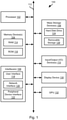
- Fig. 1 is a block diagram illustrating an example computing device 100.
- Computing device 100 may be used to perform various procedures, such as those discussed herein.
- Computing device 100 can function as a server, a client, or any other computing entity.
- Computing device can perform various monitoring functions as discussed herein, and can execute one or more application programs, such as the application programs described herein.
- Computing device 100 can be any of a wide variety of computing devices, such as a desktop computer, a notebook computer, a server computer, a handheld computer, tablet computer and the like.
- Computing device 100 includes one or more processor(s) 102, one or more memory device(s) 104, one or more interface(s) 106, one or more mass storage device(s) 108, one or more Input/Output (I/O) device(s) 110, and a display device 130 all of which are coupled to a bus 112.
- Processor(s) 102 include one or more processors or controllers that execute instructions stored in memory device(s) 104 and/or mass storage device(s) 108.
- Processor(s) 102 may also include various types of computer-readable media, such as cache memory.
- Memory device(s) 104 include various computer-readable media, such as volatile memory (e.g., random access memory (RAM) 114) and/or nonvolatile memory (e.g., read-only memory (ROM) 116). Memory device(s) 104 may also include rewritable ROM, such as Flash memory.
- volatile memory e.g., random access memory (RAM) 114
- ROM read-only memory
- Memory device(s) 104 may also include rewritable ROM, such as Flash memory.
- Mass storage device(s) 108 include various computer readable media, such as magnetic tapes, magnetic disks, optical disks, solid-state memory (e.g., Flash memory), and so forth. As shown in Fig. 1 , a particular mass storage device is a hard disk drive 124. Various drives may also be included in mass storage device(s) 108 to enable reading from and/or writing to the various computer readable media. Mass storage device(s) 108 include removable media 126 and/or non-removable media.
- I/O device(s) 110 include various devices that allow data and/or other information to be input to or retrieved from computing device 100.
- Example I/O device(s) 110 include cursor control devices, keyboards, keypads, microphones, monitors or other display devices, speakers, printers, network interface cards, modems, lenses, CCDs or other image capture devices, and the like.
- Display device 130 includes any type of device capable of displaying information to one or more users of computing device 100. Examples of display device 130 include a monitor, display terminal, video projection device, and the like.
- a graphics-processing unit (GPU) 132 may be coupled to the processor(s) 102 and/or to the display device 130.
- the GPU may be operable to render computer generated images and perform other graphical processing.
- the GPU may include some or all of the functionality of a general-purpose processor, such as the processor(s) 102.
- the GPU may also include additional functionality specific to graphics processing.
- the GPU may include hard-coded and/or hard-wired graphics function related to coordinate transformation, shading, texturing, rasterization, and other functions helpful in rendering a computer generated image.
- Interface(s) 106 include various interfaces that allow computing device 100 to interact with other systems, devices, or computing environments.
- Example interface(s) 106 include any number of different network interfaces 120, such as interfaces to local area networks (LANs), wide area networks (WANs), wireless networks, and the Internet.
- Other interface(s) include user interface 118 and peripheral device interface 122.
- the interface(s) 106 may also include one or more user interface elements 118.
- the interface(s) 106 may also include one or more peripheral interfaces such as interfaces for printers, pointing devices (mice, track pad, etc.), keyboards, and the like.
- Bus 112 allows processor(s) 102, memory device(s) 104, interface(s) 106, mass storage device(s) 108, and I/O device(s) 110 to communicate with one another, as well as other devices or components coupled to bus 112.
- Bus 112 represents one or more of several types of bus structures, such as a system bus, PCI bus, IEEE 1394 bus, USB bus, and so forth.
- programs and other executable program components are shown herein as discrete blocks, although it is understood that such programs and components may reside at various times in different storage components of computing device 100, and are executed by processor(s) 102.
- the systems and procedures described herein can be implemented in hardware, or a combination of hardware, software, and/or firmware.
- one or more application specific integrated circuits (ASICs) can be programmed to carry out one or more of the systems and procedures described herein.
- memory access commands may reference a transfer descriptor rather than a source address and/or destination address.
- Transfer descriptors are executable code that, when executed, generate a value that is then used as the address (source or destination) for a memory access commands.
- the location where the transfer descriptors are stored and the device that executes the transfer descriptors may vary.
- the processing device 102 may execute an application 200 stored in a memory device 104.
- the instructions of the application 200 may be retrieved by the processing device 102 and executed.
- the processing device 102 may retrieve the transfer descriptor from a transfer descriptor buffer 202 embodied as a separate memory device 104, e.g. a cache memory or other memory device coupled to the processor.
- the transfer descriptor buffer 202 is an area of storage within the same memory device 104 as the application 200.
- a direct memory access (DMA) controller is coupled to the processing device 102 and the memory device 104 as well as to the transfer descriptor buffer 202.
- the transfer descriptor of a memory access command may then be executed by the DMA controller 204, which may then retrieve a data value based on a result of the transfer descriptor from the memory device 104 and return it to the processing device 102 or other component.
- a separate component referred to herein as the transfer descriptor controller 206, may process transfer descriptors from the transfer descriptor buffer 202, retrieve data values according to the result of processing of the transfer descriptors and return the data values to the processing device 102.
- an instruction word executed by the processing device 102 may include some or all of the illustrated fields, including an instruction code 300, source type 302, source address 304, destination type 306, and destination address 308.
- the illustrated format for an instruction word is conventional and may be executed by many processors or memory controllers known in the art.
- the fields of the conventional instruction word are repurposed and used to implement novel transfer descriptors as described in greater detail below.
- An instruction code 300 defines an operation to be performed with respect to data retrieved from the source address 304 with the result of the operation being written to the destination address 308.
- the source type 302 is conventionally used to specify the memory device from which the source data is to be read from the source address 304.
- the destination type 306 is conventionally used to specify the memory device from which the result of the operation is to be written at the destination address 308.
- the source type 302 may refer to either a memory device or a transfer descriptor. Where the source type 302 refers to a transfer descriptor, the source address 304 is decoded to identify the transfer descriptor to execute.
- the destination address 308 is decoded to determine the transfer descriptor to execute.
- the source type 302 and destination type 306 preferably have no impact on the operation performed as specified by the instruction code 300. Stated differently, the source type 302 and destination type 306 are used exclusively to determine the data to be processed according to the operation specified by the instruction code 300 but the operation performed on the data is identical regardless of whether the data was retrieved directly from the source address 304 and destination address 308 or as the result of execution of a transfer descriptor.
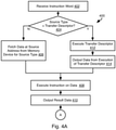
- the illustrated method 400 may be executed when processing an instruction, such as an instruction having the fields of the instruction of Fig. 3 .
- the steps of the method 400 may be executed by the processing device 102, DMA controller 204, dedicated transfer controller 206, or other component or a combination of two or more of these devices.
- the method 400 may be transparent to the processing device 102, i.e. memory access instructions may be submitted to a memory control system and responses received without any processing of transfer descriptors being performed by the processing device 102.
- the method 400 includes receiving 402 and instruction word (e.g. an instruction word 300) and evaluating 404 the source type of the instruction word. If the source type is not a transfer descriptor flag, then the data located at the source address of the instruction word is fetched 406 from the memory device 104 referenced by the source type. The operation indicated by the instruction code of the instruction word is then executed 408 and a result of the operation ("result data") is output 410.
- instruction word e.g. an instruction word 300
- a transfer descriptor is executed 412.
- a transfer descriptor corresponding to the source address of the instruction word is executed 412.
- each transfer descriptor may have an identifier and the transfer descriptor having an identifier equal to the source address of the instruction word may be executed 412.
- the result of execution 412 of the transfer descriptor is output data that is output 414 by the transfer descriptor (hereinafter a "first intermediate value").
- the operation indicated by the instruction code of the instruction word is executed 408 and the result of this operation is output 410.
- the intermediate result is an address. Accordingly, the value stored at the intermediate value in the memory device 104 is retrieved and the operation indicated by the instruction code is then executed 408 with respect to the retrieved value.
- processing of the instruction word received at step 402 may further include evaluating 416 the destination type of the instruction word. If the destination type is not a transfer descriptor flag, then the result data is written 418 to the memory device 104 indicated by the destination type of the instruction word at the destination address of the instruction word.
- the transfer descriptor identified by the destination address of the instruction word is executed 420.
- the transfer descriptor may be identified based on the destination address in the same manner that the transfer descriptor is described above as being identified for a source address.
- Execution 420 of the transfer descriptor may include an output value ("a second intermediate result").
- the second intermediate result may be an address.
- the result data of step 410 is then written 424 to the memory device 104 at the address corresponding to the second intermediate result.
- an operation only includes one operated (source or destination) accordingly, in some embodiments only the source type potentially results in execution of a transfer descriptor as described for Fig. 4A or only the destination type potentially corresponds to a transfer descriptor as described for Fig. 4B . In other instances, two transfer descriptors are executed for each instruction word as indicated by both of the source and destination types.
- the transfer descriptors provide for the customization and expansion of functions performed during a memory access function.
- functionality that may be implemented using a transfer descriptor.
- a first-in-first-out (FIFO) buffer may be implemented using transfer descriptors thereby eliminating the need for sharing of objects among multiple threads of execution accessing the FIFO buffer.
- a first transfer descriptor may maintain a write pointer indicating the current location at which new entries are to be written to the FIFO buffer.
- a second transfer descriptor may maintain a read pointer indicating the current location at which new entries are to be read from the FIFO buffer.
- the first transfer descriptor may define a function for updating the write pointer in response to write requests and for returning the current value of the pointer in response to write requests.
- the first transfer descriptor may contain the size of the buffer (e.g. number of entries) and the start address of the buffer.
- the pointer For the first transfer descriptor, receiving a write request, the pointer is incremented. If the incremented value exceeds the size of the buffer or is outside the end address of the buffer, then the pointer may be updated to point to the start address of the buffer. For the second transfer descriptor, upon receiving a read request, the pointer is updated and, if it exceeds the size of the buffer or points to an address outside the end address of the buffer, it is set to the start address of the buffer.
- an instruction may be generated by an application with an instruction code indicating a MOVE instruction, a source type set to the transfer descriptor flag, and a source address pointing to the first transfer descriptor.
- the first transfer descriptor is executed, resulting in output of the current value of the write pointer and updating of the write pointer.
- the value stored at the current value of the write pointer in the memory device 104 is then read and returned as the result of the instruction.
- an instruction maybe generated by an application with an instruction code indicating a MOVE instruction, and a destination type set to the transfer descriptor flag and a destination address pointing to the second transfer descriptor.
- the second transfer descriptor is executed, resulting in output of the current value of the read pointer and updating of the read pointer.
- a data value may then be written to the current value of the read pointer in the memory device 104.
- the transfer descriptors may include state variables that are persistent from one instruction to the next and that are updated when the transfer descriptor is called.
- an application or other software or hardware component may monitor the state variables of one or more transfer descriptors and generate events. For example, if the state variables of a transfer descriptor indicate that a threshold condition is met, then one or more threads may be blocked, branch to a different thread of execution, be started or instantiate, or be subject to other thread management functions.
- the read pointer and write pointer of transfer descriptors defining a FIFO buffer as described above may be compared, if the read pointer is less than a threshold value offset from than the write pointer, then the buffer may be deemed to be almost empty and threads attempting to make requests to the FIFO buffer may be blocked until the threshold is found to be exceeded. Likewise, where the read pointer is above a second threshold amount offset from the write pointer, the FIFO buffer may be deemed to be almost full and threads attempting to write to the FIFO buffer may be blocked until the second threshold is no longer exceeded.
Landscapes
- Engineering & Computer Science (AREA)
- Theoretical Computer Science (AREA)
- Software Systems (AREA)
- General Engineering & Computer Science (AREA)
- General Physics & Mathematics (AREA)
- Physics & Mathematics (AREA)
- Human Computer Interaction (AREA)
- Computer Hardware Design (AREA)
- Microelectronics & Electronic Packaging (AREA)
- Bus Control (AREA)
- Advance Control (AREA)
- Executing Machine-Instructions (AREA)
- Memory System (AREA)
- Information Retrieval, Db Structures And Fs Structures Therefor (AREA)
- Information Transfer Between Computers (AREA)
Applications Claiming Priority (2)
| Application Number | Priority Date | Filing Date | Title |
|---|---|---|---|
| US14/934,707 US9977619B2 (en) | 2015-11-06 | 2015-11-06 | Transfer descriptor for memory access commands |
| PCT/US2016/060995 WO2017079769A1 (en) | 2015-11-06 | 2016-11-08 | Transfer descriptor for memory access commands |
Publications (3)
| Publication Number | Publication Date |
|---|---|
| EP3398075A1 EP3398075A1 (en) | 2018-11-07 |
| EP3398075A4 EP3398075A4 (en) | 2019-07-10 |
| EP3398075B1 true EP3398075B1 (en) | 2022-02-16 |
Family
ID=58663110
Family Applications (1)
| Application Number | Title | Priority Date | Filing Date |
|---|---|---|---|
| EP16863185.1A Active EP3398075B1 (en) | 2015-11-06 | 2016-11-08 | Transfer descriptor for memory access commands |
Country Status (6)
| Country | Link |
|---|---|
| US (1) | US9977619B2 (enExample) |
| EP (1) | EP3398075B1 (enExample) |
| JP (1) | JP6888019B2 (enExample) |
| KR (1) | KR102632382B1 (enExample) |
| CN (1) | CN108292277B (enExample) |
| WO (1) | WO2017079769A1 (enExample) |
Families Citing this family (11)
| Publication number | Priority date | Publication date | Assignee | Title |
|---|---|---|---|---|
| CN113805813B (zh) * | 2018-11-30 | 2024-07-16 | 北京忆芯科技有限公司 | 降低读命令处理延迟的方法与装置 |
| CN111831337B (zh) * | 2019-04-19 | 2022-11-29 | 安徽寒武纪信息科技有限公司 | 数据同步方法及装置以及相关产品 |
| CN111782267B (zh) * | 2019-04-04 | 2022-12-09 | 安徽寒武纪信息科技有限公司 | 数据处理方法及装置以及相关产品 |
| CN111831329B (zh) * | 2019-04-19 | 2022-12-09 | 安徽寒武纪信息科技有限公司 | 数据处理方法及装置以及相关产品 |
| CN112347186B (zh) * | 2019-08-09 | 2023-02-28 | 安徽寒武纪信息科技有限公司 | 数据同步方法及装置以及相关产品 |
| CN111782577B (zh) * | 2019-04-04 | 2023-03-24 | 安徽寒武纪信息科技有限公司 | 数据处理装置及方法以及相关产品 |
| US11243699B2 (en) * | 2019-05-22 | 2022-02-08 | Micron Technology, Inc. | System using a restricted operation mode memory indicator |
| CN110457232A (zh) * | 2019-07-31 | 2019-11-15 | 联想(北京)有限公司 | 数据处理方法、装置、计算设备及介质 |
| US11221776B2 (en) * | 2019-12-30 | 2022-01-11 | Micron Technology, Inc. | Metadata indication for a memory device |
| US11385820B2 (en) * | 2020-03-04 | 2022-07-12 | Micron Technology, Inc. | Command batching for a memory sub-system |
| CN117992123B (zh) * | 2024-04-02 | 2024-07-05 | 摩尔线程智能科技(北京)有限责任公司 | 指令执行方法、装置、电子设备、存储介质 |
Family Cites Families (25)
| Publication number | Priority date | Publication date | Assignee | Title |
|---|---|---|---|---|
| US3739352A (en) | 1971-06-28 | 1973-06-12 | Burroughs Corp | Variable word width processor control |
| US5761740A (en) | 1995-11-30 | 1998-06-02 | Unisys Corporation | Method of and apparatus for rapidly loading addressing registers |
| US5941959A (en) | 1995-12-20 | 1999-08-24 | Tandem Computers Incorporated | System for transferring a data stream to a requestor without copying data segments to each one of multiple data source/sinks during data stream building |
| US5961639A (en) | 1996-12-16 | 1999-10-05 | International Business Machines Corporation | Processor and method for dynamically inserting auxiliary instructions within an instruction stream during execution |
| US6115761A (en) | 1997-05-30 | 2000-09-05 | Lsi Logic Corporation | First-In-First-Out (FIFO) memories having dual descriptors and credit passing for efficient access in a multi-processor system environment |
| US6145016A (en) | 1998-09-03 | 2000-11-07 | Advanced Micro Devices, Inc. | System for transferring frame data by transferring the descriptor index data to identify a specified amount of data to be transferred stored in the host computer |
| US6434649B1 (en) | 1998-10-14 | 2002-08-13 | Hitachi, Ltd. | Data streamer |
| US6754732B1 (en) * | 2001-08-03 | 2004-06-22 | Intervoice Limited Partnership | System and method for efficient data transfer management |
| US7363467B2 (en) | 2002-01-03 | 2008-04-22 | Intel Corporation | Dependence-chain processing using trace descriptors having dependency descriptors |
| ATE369587T1 (de) | 2003-05-15 | 2007-08-15 | Nxp Bv | Usb host controller mit speicher für transferdeskriptoren |
| JP4340519B2 (ja) * | 2003-11-04 | 2009-10-07 | 富士通株式会社 | 情報処理端末 |
| US7293121B2 (en) | 2004-02-25 | 2007-11-06 | Analog Devices, Inc. | DMA controller utilizing flexible DMA descriptors |
| US7496695B2 (en) | 2005-09-29 | 2009-02-24 | P.A. Semi, Inc. | Unified DMA |
| US8683143B2 (en) * | 2005-12-30 | 2014-03-25 | Intel Corporation | Unbounded transactional memory systems |
| US20090119460A1 (en) * | 2007-11-07 | 2009-05-07 | Infineon Technologies Ag | Storing Portions of a Data Transfer Descriptor in Cached and Uncached Address Space |
| US7877524B1 (en) * | 2007-11-23 | 2011-01-25 | Pmc-Sierra Us, Inc. | Logical address direct memory access with multiple concurrent physical ports and internal switching |
| JP5287301B2 (ja) | 2009-01-30 | 2013-09-11 | 富士通株式会社 | ディスクリプタ転送装置、i/oコントローラ、及びディスクリプタ転送方法 |
| US8549182B2 (en) * | 2010-06-23 | 2013-10-01 | International Business Machines Corporation | Store/store block instructions for communicating with adapters |
| JP2012014436A (ja) * | 2010-06-30 | 2012-01-19 | Toshiba Corp | ダイレクトメモリアクセス制御装置及び方法 |
| US9552206B2 (en) | 2010-11-18 | 2017-01-24 | Texas Instruments Incorporated | Integrated circuit with control node circuitry and processing circuitry |
| US9436629B2 (en) * | 2011-11-15 | 2016-09-06 | Marvell World Trade Ltd. | Dynamic boot image streaming |
| CN104247436A (zh) * | 2012-04-25 | 2014-12-24 | 三星电子株式会社 | 在数字广播系统中用于发送和接收的信令信息的装置和方法 |
| US20140181427A1 (en) * | 2012-12-21 | 2014-06-26 | Advanced Micro Devices, Inc. | Compound Memory Operations in a Logic Layer of a Stacked Memory |
| CN103593437A (zh) * | 2013-11-14 | 2014-02-19 | 浪潮电子信息产业股份有限公司 | 一种基于dma的数据压缩芯片结构及其实现方法 |
| US9785565B2 (en) * | 2014-06-30 | 2017-10-10 | Microunity Systems Engineering, Inc. | System and methods for expandably wide processor instructions |
-
2015
- 2015-11-06 US US14/934,707 patent/US9977619B2/en active Active
-
2016
- 2016-11-08 JP JP2018543080A patent/JP6888019B2/ja active Active
- 2016-11-08 CN CN201680070312.7A patent/CN108292277B/zh active Active
- 2016-11-08 KR KR1020187013674A patent/KR102632382B1/ko active Active
- 2016-11-08 EP EP16863185.1A patent/EP3398075B1/en active Active
- 2016-11-08 WO PCT/US2016/060995 patent/WO2017079769A1/en not_active Ceased
Non-Patent Citations (1)
| Title |
|---|
| None * |
Also Published As
| Publication number | Publication date |
|---|---|
| KR102632382B1 (ko) | 2024-01-31 |
| JP2018537800A (ja) | 2018-12-20 |
| EP3398075A4 (en) | 2019-07-10 |
| US9977619B2 (en) | 2018-05-22 |
| EP3398075A1 (en) | 2018-11-07 |
| US20170131939A1 (en) | 2017-05-11 |
| JP6888019B2 (ja) | 2021-06-16 |
| CN108292277B (zh) | 2021-08-17 |
| KR20200028280A (ko) | 2020-03-16 |
| CN108292277A (zh) | 2018-07-17 |
| WO2017079769A1 (en) | 2017-05-11 |
Similar Documents
| Publication | Publication Date | Title |
|---|---|---|
| EP3398075B1 (en) | Transfer descriptor for memory access commands | |
| US10831547B2 (en) | Accelerator control apparatus for analyzing big data, accelerator control method, and program | |
| JP2023534283A5 (enExample) | ||
| US10585623B2 (en) | Software defined FIFO buffer for multithreaded access | |
| US9128615B2 (en) | Storage systems that create snapshot queues | |
| US10564889B2 (en) | Method and apparatus for processing data based on physical host | |
| US20160328816A1 (en) | Gpu operation | |
| US10083127B2 (en) | Self-ordering buffer | |
| CN111625281A (zh) | 一种数据处理方法、装置、设备及存储介质 | |
| US8898625B2 (en) | Optimized storage of function variables | |
| US9081487B2 (en) | System and method for manipulating an image | |
| EP3387524B1 (en) | Hardware access counters and event generation for coordinating multithreaded processing | |
| CN116991600B (zh) | 图形调用指令的处理方法、装置、设备及存储介质 | |
| CN107967222A (zh) | 一种SPI-Nand查找数据页的方法及装置 | |
| CN109460511A (zh) | 一种获取用户画像的方法、装置、电子设备及存储介质 | |
| US10186071B2 (en) | Rendering system and method for generating ray | |
| RU2656719C2 (ru) | Скорость операции в виде динамической линии уровня | |
| CN113806288A (zh) | 适用于SoC内核之间的数据交互方法、装置及电子设备 | |
| US20170337389A1 (en) | Method and apparatus for obtaining geographical location information, and electronic terminal |
Legal Events
| Date | Code | Title | Description |
|---|---|---|---|
| STAA | Information on the status of an ep patent application or granted ep patent |
Free format text: STATUS: THE INTERNATIONAL PUBLICATION HAS BEEN MADE |
|
| PUAI | Public reference made under article 153(3) epc to a published international application that has entered the european phase |
Free format text: ORIGINAL CODE: 0009012 |
|
| STAA | Information on the status of an ep patent application or granted ep patent |
Free format text: STATUS: REQUEST FOR EXAMINATION WAS MADE |
|
| 17P | Request for examination filed |
Effective date: 20180606 |
|
| AK | Designated contracting states |
Kind code of ref document: A1 Designated state(s): AL AT BE BG CH CY CZ DE DK EE ES FI FR GB GR HR HU IE IS IT LI LT LU LV MC MK MT NL NO PL PT RO RS SE SI SK SM TR |
|
| AX | Request for extension of the european patent |
Extension state: BA ME |
|
| REG | Reference to a national code |
Ref country code: DE Ref legal event code: R079 Ref document number: 602016069237 Country of ref document: DE Free format text: PREVIOUS MAIN CLASS: G06F0013000000 Ipc: G06F0009300000 |
|
| A4 | Supplementary search report drawn up and despatched |
Effective date: 20190607 |
|
| RIC1 | Information provided on ipc code assigned before grant |
Ipc: G06F 13/12 20060101ALI20190603BHEP Ipc: G06F 9/30 20180101AFI20190603BHEP |
|
| DAV | Request for validation of the european patent (deleted) | ||
| DAX | Request for extension of the european patent (deleted) | ||
| STAA | Information on the status of an ep patent application or granted ep patent |
Free format text: STATUS: EXAMINATION IS IN PROGRESS |
|
| 17Q | First examination report despatched |
Effective date: 20200608 |
|
| GRAP | Despatch of communication of intention to grant a patent |
Free format text: ORIGINAL CODE: EPIDOSNIGR1 |
|
| STAA | Information on the status of an ep patent application or granted ep patent |
Free format text: STATUS: GRANT OF PATENT IS INTENDED |
|
| INTG | Intention to grant announced |
Effective date: 20210728 |
|
| GRAJ | Information related to disapproval of communication of intention to grant by the applicant or resumption of examination proceedings by the epo deleted |
Free format text: ORIGINAL CODE: EPIDOSDIGR1 |
|
| STAA | Information on the status of an ep patent application or granted ep patent |
Free format text: STATUS: EXAMINATION IS IN PROGRESS |
|
| INTC | Intention to grant announced (deleted) | ||
| GRAP | Despatch of communication of intention to grant a patent |
Free format text: ORIGINAL CODE: EPIDOSNIGR1 |
|
| STAA | Information on the status of an ep patent application or granted ep patent |
Free format text: STATUS: GRANT OF PATENT IS INTENDED |
|
| GRAS | Grant fee paid |
Free format text: ORIGINAL CODE: EPIDOSNIGR3 |
|
| INTG | Intention to grant announced |
Effective date: 20211213 |
|
| GRAA | (expected) grant |
Free format text: ORIGINAL CODE: 0009210 |
|
| STAA | Information on the status of an ep patent application or granted ep patent |
Free format text: STATUS: THE PATENT HAS BEEN GRANTED |
|
| AK | Designated contracting states |
Kind code of ref document: B1 Designated state(s): AL AT BE BG CH CY CZ DE DK EE ES FI FR GB GR HR HU IE IS IT LI LT LU LV MC MK MT NL NO PL PT RO RS SE SI SK SM TR |
|
| REG | Reference to a national code |
Ref country code: GB Ref legal event code: FG4D |
|
| REG | Reference to a national code |
Ref country code: CH Ref legal event code: EP |
|
| REG | Reference to a national code |
Ref country code: DE Ref legal event code: R096 Ref document number: 602016069237 Country of ref document: DE |
|
| REG | Reference to a national code |
Ref country code: AT Ref legal event code: REF Ref document number: 1469311 Country of ref document: AT Kind code of ref document: T Effective date: 20220315 |
|
| REG | Reference to a national code |
Ref country code: IE Ref legal event code: FG4D |
|
| REG | Reference to a national code |
Ref country code: LT Ref legal event code: MG9D |
|
| REG | Reference to a national code |
Ref country code: NL Ref legal event code: MP Effective date: 20220216 |
|
| REG | Reference to a national code |
Ref country code: AT Ref legal event code: MK05 Ref document number: 1469311 Country of ref document: AT Kind code of ref document: T Effective date: 20220216 |
|
| PG25 | Lapsed in a contracting state [announced via postgrant information from national office to epo] |
Ref country code: SE Free format text: LAPSE BECAUSE OF FAILURE TO SUBMIT A TRANSLATION OF THE DESCRIPTION OR TO PAY THE FEE WITHIN THE PRESCRIBED TIME-LIMIT Effective date: 20220216 Ref country code: RS Free format text: LAPSE BECAUSE OF FAILURE TO SUBMIT A TRANSLATION OF THE DESCRIPTION OR TO PAY THE FEE WITHIN THE PRESCRIBED TIME-LIMIT Effective date: 20220216 Ref country code: PT Free format text: LAPSE BECAUSE OF FAILURE TO SUBMIT A TRANSLATION OF THE DESCRIPTION OR TO PAY THE FEE WITHIN THE PRESCRIBED TIME-LIMIT Effective date: 20220616 Ref country code: NO Free format text: LAPSE BECAUSE OF FAILURE TO SUBMIT A TRANSLATION OF THE DESCRIPTION OR TO PAY THE FEE WITHIN THE PRESCRIBED TIME-LIMIT Effective date: 20220516 Ref country code: NL Free format text: LAPSE BECAUSE OF FAILURE TO SUBMIT A TRANSLATION OF THE DESCRIPTION OR TO PAY THE FEE WITHIN THE PRESCRIBED TIME-LIMIT Effective date: 20220216 Ref country code: LT Free format text: LAPSE BECAUSE OF FAILURE TO SUBMIT A TRANSLATION OF THE DESCRIPTION OR TO PAY THE FEE WITHIN THE PRESCRIBED TIME-LIMIT Effective date: 20220216 Ref country code: HR Free format text: LAPSE BECAUSE OF FAILURE TO SUBMIT A TRANSLATION OF THE DESCRIPTION OR TO PAY THE FEE WITHIN THE PRESCRIBED TIME-LIMIT Effective date: 20220216 Ref country code: ES Free format text: LAPSE BECAUSE OF FAILURE TO SUBMIT A TRANSLATION OF THE DESCRIPTION OR TO PAY THE FEE WITHIN THE PRESCRIBED TIME-LIMIT Effective date: 20220216 Ref country code: BG Free format text: LAPSE BECAUSE OF FAILURE TO SUBMIT A TRANSLATION OF THE DESCRIPTION OR TO PAY THE FEE WITHIN THE PRESCRIBED TIME-LIMIT Effective date: 20220516 |
|
| PG25 | Lapsed in a contracting state [announced via postgrant information from national office to epo] |
Ref country code: PL Free format text: LAPSE BECAUSE OF FAILURE TO SUBMIT A TRANSLATION OF THE DESCRIPTION OR TO PAY THE FEE WITHIN THE PRESCRIBED TIME-LIMIT Effective date: 20220216 Ref country code: LV Free format text: LAPSE BECAUSE OF FAILURE TO SUBMIT A TRANSLATION OF THE DESCRIPTION OR TO PAY THE FEE WITHIN THE PRESCRIBED TIME-LIMIT Effective date: 20220216 Ref country code: GR Free format text: LAPSE BECAUSE OF FAILURE TO SUBMIT A TRANSLATION OF THE DESCRIPTION OR TO PAY THE FEE WITHIN THE PRESCRIBED TIME-LIMIT Effective date: 20220517 Ref country code: FI Free format text: LAPSE BECAUSE OF FAILURE TO SUBMIT A TRANSLATION OF THE DESCRIPTION OR TO PAY THE FEE WITHIN THE PRESCRIBED TIME-LIMIT Effective date: 20220216 Ref country code: AT Free format text: LAPSE BECAUSE OF FAILURE TO SUBMIT A TRANSLATION OF THE DESCRIPTION OR TO PAY THE FEE WITHIN THE PRESCRIBED TIME-LIMIT Effective date: 20220216 |
|
| PG25 | Lapsed in a contracting state [announced via postgrant information from national office to epo] |
Ref country code: IS Free format text: LAPSE BECAUSE OF FAILURE TO SUBMIT A TRANSLATION OF THE DESCRIPTION OR TO PAY THE FEE WITHIN THE PRESCRIBED TIME-LIMIT Effective date: 20220617 |
|
| PG25 | Lapsed in a contracting state [announced via postgrant information from national office to epo] |
Ref country code: SM Free format text: LAPSE BECAUSE OF FAILURE TO SUBMIT A TRANSLATION OF THE DESCRIPTION OR TO PAY THE FEE WITHIN THE PRESCRIBED TIME-LIMIT Effective date: 20220216 Ref country code: SK Free format text: LAPSE BECAUSE OF FAILURE TO SUBMIT A TRANSLATION OF THE DESCRIPTION OR TO PAY THE FEE WITHIN THE PRESCRIBED TIME-LIMIT Effective date: 20220216 Ref country code: RO Free format text: LAPSE BECAUSE OF FAILURE TO SUBMIT A TRANSLATION OF THE DESCRIPTION OR TO PAY THE FEE WITHIN THE PRESCRIBED TIME-LIMIT Effective date: 20220216 Ref country code: EE Free format text: LAPSE BECAUSE OF FAILURE TO SUBMIT A TRANSLATION OF THE DESCRIPTION OR TO PAY THE FEE WITHIN THE PRESCRIBED TIME-LIMIT Effective date: 20220216 Ref country code: DK Free format text: LAPSE BECAUSE OF FAILURE TO SUBMIT A TRANSLATION OF THE DESCRIPTION OR TO PAY THE FEE WITHIN THE PRESCRIBED TIME-LIMIT Effective date: 20220216 Ref country code: CZ Free format text: LAPSE BECAUSE OF FAILURE TO SUBMIT A TRANSLATION OF THE DESCRIPTION OR TO PAY THE FEE WITHIN THE PRESCRIBED TIME-LIMIT Effective date: 20220216 |
|
| REG | Reference to a national code |
Ref country code: DE Ref legal event code: R097 Ref document number: 602016069237 Country of ref document: DE |
|
| PG25 | Lapsed in a contracting state [announced via postgrant information from national office to epo] |
Ref country code: AL Free format text: LAPSE BECAUSE OF FAILURE TO SUBMIT A TRANSLATION OF THE DESCRIPTION OR TO PAY THE FEE WITHIN THE PRESCRIBED TIME-LIMIT Effective date: 20220216 |
|
| PLBE | No opposition filed within time limit |
Free format text: ORIGINAL CODE: 0009261 |
|
| STAA | Information on the status of an ep patent application or granted ep patent |
Free format text: STATUS: NO OPPOSITION FILED WITHIN TIME LIMIT |
|
| 26N | No opposition filed |
Effective date: 20221117 |
|
| PG25 | Lapsed in a contracting state [announced via postgrant information from national office to epo] |
Ref country code: SI Free format text: LAPSE BECAUSE OF FAILURE TO SUBMIT A TRANSLATION OF THE DESCRIPTION OR TO PAY THE FEE WITHIN THE PRESCRIBED TIME-LIMIT Effective date: 20220216 |
|
| P01 | Opt-out of the competence of the unified patent court (upc) registered |
Effective date: 20230513 |
|
| PG25 | Lapsed in a contracting state [announced via postgrant information from national office to epo] |
Ref country code: MC Free format text: LAPSE BECAUSE OF FAILURE TO SUBMIT A TRANSLATION OF THE DESCRIPTION OR TO PAY THE FEE WITHIN THE PRESCRIBED TIME-LIMIT Effective date: 20220216 |
|
| REG | Reference to a national code |
Ref country code: CH Ref legal event code: PL |
|
| REG | Reference to a national code |
Ref country code: BE Ref legal event code: MM Effective date: 20221130 |
|
| PG25 | Lapsed in a contracting state [announced via postgrant information from national office to epo] |
Ref country code: LI Free format text: LAPSE BECAUSE OF NON-PAYMENT OF DUE FEES Effective date: 20221130 Ref country code: IT Free format text: LAPSE BECAUSE OF FAILURE TO SUBMIT A TRANSLATION OF THE DESCRIPTION OR TO PAY THE FEE WITHIN THE PRESCRIBED TIME-LIMIT Effective date: 20220216 Ref country code: CH Free format text: LAPSE BECAUSE OF NON-PAYMENT OF DUE FEES Effective date: 20221130 |
|
| PG25 | Lapsed in a contracting state [announced via postgrant information from national office to epo] |
Ref country code: LU Free format text: LAPSE BECAUSE OF NON-PAYMENT OF DUE FEES Effective date: 20221108 |
|
| PG25 | Lapsed in a contracting state [announced via postgrant information from national office to epo] |
Ref country code: IE Free format text: LAPSE BECAUSE OF NON-PAYMENT OF DUE FEES Effective date: 20221108 |
|
| PG25 | Lapsed in a contracting state [announced via postgrant information from national office to epo] |
Ref country code: BE Free format text: LAPSE BECAUSE OF NON-PAYMENT OF DUE FEES Effective date: 20221130 |
|
| PG25 | Lapsed in a contracting state [announced via postgrant information from national office to epo] |
Ref country code: HU Free format text: LAPSE BECAUSE OF FAILURE TO SUBMIT A TRANSLATION OF THE DESCRIPTION OR TO PAY THE FEE WITHIN THE PRESCRIBED TIME-LIMIT; INVALID AB INITIO Effective date: 20161108 |
|
| PG25 | Lapsed in a contracting state [announced via postgrant information from national office to epo] |
Ref country code: CY Free format text: LAPSE BECAUSE OF FAILURE TO SUBMIT A TRANSLATION OF THE DESCRIPTION OR TO PAY THE FEE WITHIN THE PRESCRIBED TIME-LIMIT Effective date: 20220216 |
|
| PG25 | Lapsed in a contracting state [announced via postgrant information from national office to epo] |
Ref country code: MK Free format text: LAPSE BECAUSE OF FAILURE TO SUBMIT A TRANSLATION OF THE DESCRIPTION OR TO PAY THE FEE WITHIN THE PRESCRIBED TIME-LIMIT Effective date: 20220216 |
|
| PG25 | Lapsed in a contracting state [announced via postgrant information from national office to epo] |
Ref country code: TR Free format text: LAPSE BECAUSE OF FAILURE TO SUBMIT A TRANSLATION OF THE DESCRIPTION OR TO PAY THE FEE WITHIN THE PRESCRIBED TIME-LIMIT Effective date: 20220216 |
|
| PG25 | Lapsed in a contracting state [announced via postgrant information from national office to epo] |
Ref country code: MT Free format text: LAPSE BECAUSE OF FAILURE TO SUBMIT A TRANSLATION OF THE DESCRIPTION OR TO PAY THE FEE WITHIN THE PRESCRIBED TIME-LIMIT Effective date: 20220216 |
|
| PGFP | Annual fee paid to national office [announced via postgrant information from national office to epo] |
Ref country code: DE Payment date: 20251128 Year of fee payment: 10 |
|
| PGFP | Annual fee paid to national office [announced via postgrant information from national office to epo] |
Ref country code: GB Payment date: 20251120 Year of fee payment: 10 |
|
| PGFP | Annual fee paid to national office [announced via postgrant information from national office to epo] |
Ref country code: FR Payment date: 20251125 Year of fee payment: 10 |