EP3398053B1 - Processor instructions to accelerate fec encoding and decoding - Google Patents
Processor instructions to accelerate fec encoding and decoding Download PDFInfo
- Publication number
- EP3398053B1 EP3398053B1 EP16826852.2A EP16826852A EP3398053B1 EP 3398053 B1 EP3398053 B1 EP 3398053B1 EP 16826852 A EP16826852 A EP 16826852A EP 3398053 B1 EP3398053 B1 EP 3398053B1
- Authority
- EP
- European Patent Office
- Prior art keywords
- input
- instruction
- value
- operand
- processing element
- Prior art date
- Legal status (The legal status is an assumption and is not a legal conclusion. Google has not performed a legal analysis and makes no representation as to the accuracy of the status listed.)
- Active
Links
- 230000006870 function Effects 0.000 claims description 195
- 238000012545 processing Methods 0.000 claims description 166
- 230000015654 memory Effects 0.000 claims description 115
- 230000037361 pathway Effects 0.000 claims description 43
- 238000000034 method Methods 0.000 claims description 24
- 230000004044 response Effects 0.000 claims description 22
- 230000008569 process Effects 0.000 claims description 5
- 230000009977 dual effect Effects 0.000 description 30
- 238000004891 communication Methods 0.000 description 16
- 238000010586 diagram Methods 0.000 description 10
- 230000009471 action Effects 0.000 description 6
- 235000019800 disodium phosphate Nutrition 0.000 description 6
- 238000012546 transfer Methods 0.000 description 6
- 241000169170 Boreogadus saida Species 0.000 description 3
- 238000003491 array Methods 0.000 description 3
- 238000012986 modification Methods 0.000 description 3
- 230000004048 modification Effects 0.000 description 3
- 230000003287 optical effect Effects 0.000 description 3
- 238000013459 approach Methods 0.000 description 2
- 230000005540 biological transmission Effects 0.000 description 2
- 238000004422 calculation algorithm Methods 0.000 description 2
- 230000008867 communication pathway Effects 0.000 description 2
- 238000013461 design Methods 0.000 description 2
- 239000004744 fabric Substances 0.000 description 2
- 229920006395 saturated elastomer Polymers 0.000 description 2
- 238000013515 script Methods 0.000 description 2
- 238000012360 testing method Methods 0.000 description 2
- 108091006503 SLC26A1 Proteins 0.000 description 1
- 230000006399 behavior Effects 0.000 description 1
- 230000009286 beneficial effect Effects 0.000 description 1
- 230000008901 benefit Effects 0.000 description 1
- 230000003139 buffering effect Effects 0.000 description 1
- 238000004364 calculation method Methods 0.000 description 1
- 230000010267 cellular communication Effects 0.000 description 1
- 230000001413 cellular effect Effects 0.000 description 1
- 239000000919 ceramic Substances 0.000 description 1
- 230000008859 change Effects 0.000 description 1
- 238000012937 correction Methods 0.000 description 1
- 238000013500 data storage Methods 0.000 description 1
- 230000001419 dependent effect Effects 0.000 description 1
- 238000010894 electron beam technology Methods 0.000 description 1
- 239000000284 extract Substances 0.000 description 1
- 230000006872 improvement Effects 0.000 description 1
- 238000009434 installation Methods 0.000 description 1
- 230000001788 irregular Effects 0.000 description 1
- 238000007726 management method Methods 0.000 description 1
- 230000007246 mechanism Effects 0.000 description 1
- 238000005457 optimization Methods 0.000 description 1
- 239000002245 particle Substances 0.000 description 1
- 230000001902 propagating effect Effects 0.000 description 1
- 239000000758 substrate Substances 0.000 description 1
Images


Classifications
-
- G—PHYSICS
- G06—COMPUTING; CALCULATING OR COUNTING
- G06F—ELECTRIC DIGITAL DATA PROCESSING
- G06F9/00—Arrangements for program control, e.g. control units
- G06F9/06—Arrangements for program control, e.g. control units using stored programs, i.e. using an internal store of processing equipment to receive or retain programs
- G06F9/30—Arrangements for executing machine instructions, e.g. instruction decode
- G06F9/30003—Arrangements for executing specific machine instructions
- G06F9/30007—Arrangements for executing specific machine instructions to perform operations on data operands
- G06F9/3001—Arithmetic instructions
-
- G—PHYSICS
- G06—COMPUTING; CALCULATING OR COUNTING
- G06F—ELECTRIC DIGITAL DATA PROCESSING
- G06F17/00—Digital computing or data processing equipment or methods, specially adapted for specific functions
- G06F17/10—Complex mathematical operations
- G06F17/18—Complex mathematical operations for evaluating statistical data, e.g. average values, frequency distributions, probability functions, regression analysis
-
- G—PHYSICS
- G06—COMPUTING; CALCULATING OR COUNTING
- G06F—ELECTRIC DIGITAL DATA PROCESSING
- G06F9/00—Arrangements for program control, e.g. control units
- G06F9/06—Arrangements for program control, e.g. control units using stored programs, i.e. using an internal store of processing equipment to receive or retain programs
- G06F9/30—Arrangements for executing machine instructions, e.g. instruction decode
- G06F9/30003—Arrangements for executing specific machine instructions
- G06F9/30007—Arrangements for executing specific machine instructions to perform operations on data operands
- G06F9/30021—Compare instructions, e.g. Greater-Than, Equal-To, MINMAX
-
- G—PHYSICS
- G06—COMPUTING; CALCULATING OR COUNTING
- G06F—ELECTRIC DIGITAL DATA PROCESSING
- G06F9/00—Arrangements for program control, e.g. control units
- G06F9/06—Arrangements for program control, e.g. control units using stored programs, i.e. using an internal store of processing equipment to receive or retain programs
- G06F9/30—Arrangements for executing machine instructions, e.g. instruction decode
- G06F9/30003—Arrangements for executing specific machine instructions
- G06F9/30007—Arrangements for executing specific machine instructions to perform operations on data operands
- G06F9/30036—Instructions to perform operations on packed data, e.g. vector, tile or matrix operations
-
- G—PHYSICS
- G06—COMPUTING; CALCULATING OR COUNTING
- G06F—ELECTRIC DIGITAL DATA PROCESSING
- G06F9/00—Arrangements for program control, e.g. control units
- G06F9/06—Arrangements for program control, e.g. control units using stored programs, i.e. using an internal store of processing equipment to receive or retain programs
- G06F9/30—Arrangements for executing machine instructions, e.g. instruction decode
- G06F9/30003—Arrangements for executing specific machine instructions
- G06F9/3004—Arrangements for executing specific machine instructions to perform operations on memory
-
- G—PHYSICS
- G06—COMPUTING; CALCULATING OR COUNTING
- G06F—ELECTRIC DIGITAL DATA PROCESSING
- G06F9/00—Arrangements for program control, e.g. control units
- G06F9/06—Arrangements for program control, e.g. control units using stored programs, i.e. using an internal store of processing equipment to receive or retain programs
- G06F9/30—Arrangements for executing machine instructions, e.g. instruction decode
- G06F9/30003—Arrangements for executing specific machine instructions
- G06F9/3005—Arrangements for executing specific machine instructions to perform operations for flow control
- G06F9/30065—Loop control instructions; iterative instructions, e.g. LOOP, REPEAT
-
- G—PHYSICS
- G06—COMPUTING; CALCULATING OR COUNTING
- G06F—ELECTRIC DIGITAL DATA PROCESSING
- G06F9/00—Arrangements for program control, e.g. control units
- G06F9/06—Arrangements for program control, e.g. control units using stored programs, i.e. using an internal store of processing equipment to receive or retain programs
- G06F9/30—Arrangements for executing machine instructions, e.g. instruction decode
- G06F9/30098—Register arrangements
-
- G—PHYSICS
- G06—COMPUTING; CALCULATING OR COUNTING
- G06F—ELECTRIC DIGITAL DATA PROCESSING
- G06F9/00—Arrangements for program control, e.g. control units
- G06F9/06—Arrangements for program control, e.g. control units using stored programs, i.e. using an internal store of processing equipment to receive or retain programs
- G06F9/30—Arrangements for executing machine instructions, e.g. instruction decode
- G06F9/38—Concurrent instruction execution, e.g. pipeline, look ahead
- G06F9/3867—Concurrent instruction execution, e.g. pipeline, look ahead using instruction pipelines
- G06F9/3869—Implementation aspects, e.g. pipeline latches; pipeline synchronisation and clocking
-
- G—PHYSICS
- G06—COMPUTING; CALCULATING OR COUNTING
- G06F—ELECTRIC DIGITAL DATA PROCESSING
- G06F9/00—Arrangements for program control, e.g. control units
- G06F9/06—Arrangements for program control, e.g. control units using stored programs, i.e. using an internal store of processing equipment to receive or retain programs
- G06F9/30—Arrangements for executing machine instructions, e.g. instruction decode
- G06F9/38—Concurrent instruction execution, e.g. pipeline, look ahead
- G06F9/3885—Concurrent instruction execution, e.g. pipeline, look ahead using a plurality of independent parallel functional units
- G06F9/3887—Concurrent instruction execution, e.g. pipeline, look ahead using a plurality of independent parallel functional units controlled by a single instruction for multiple data lanes [SIMD]
-
- G—PHYSICS
- G06—COMPUTING; CALCULATING OR COUNTING
- G06F—ELECTRIC DIGITAL DATA PROCESSING
- G06F9/00—Arrangements for program control, e.g. control units
- G06F9/06—Arrangements for program control, e.g. control units using stored programs, i.e. using an internal store of processing equipment to receive or retain programs
- G06F9/30—Arrangements for executing machine instructions, e.g. instruction decode
- G06F9/38—Concurrent instruction execution, e.g. pipeline, look ahead
- G06F9/3885—Concurrent instruction execution, e.g. pipeline, look ahead using a plurality of independent parallel functional units
- G06F9/3893—Concurrent instruction execution, e.g. pipeline, look ahead using a plurality of independent parallel functional units controlled in tandem, e.g. multiplier-accumulator
Landscapes
- Engineering & Computer Science (AREA)
- Theoretical Computer Science (AREA)
- Software Systems (AREA)
- Physics & Mathematics (AREA)
- General Physics & Mathematics (AREA)
- General Engineering & Computer Science (AREA)
- Computational Mathematics (AREA)
- Mathematical Analysis (AREA)
- Mathematical Optimization (AREA)
- Pure & Applied Mathematics (AREA)
- Mathematical Physics (AREA)
- Data Mining & Analysis (AREA)
- Bioinformatics & Cheminformatics (AREA)
- Bioinformatics & Computational Biology (AREA)
- Life Sciences & Earth Sciences (AREA)
- Evolutionary Biology (AREA)
- Operations Research (AREA)
- Probability & Statistics with Applications (AREA)
- Algebra (AREA)
- Databases & Information Systems (AREA)
- Advance Control (AREA)
- Executing Machine-Instructions (AREA)
- Detection And Prevention Of Errors In Transmission (AREA)
- Detection And Correction Of Errors (AREA)
Description
- The field of the invention generally relates to processor instructions in a software-configurable processing element.
- Forward Error Correction (FEC) is a popular method to minimize errors in a wireless, wired or any other communication channel. FEC could be implemented by a FEC Encoder on transmit side of the channel and FEC Decoder on the receive side of the communication channel. Many FEC encoding and decoding methods require significant computation and, at the same time, need to be performed in "real-time", i.e. sustain communication speeds required for a chosen application.
- FEC may be performed using codes, where input data is encoded into a codeword and transmitted to a receiver that decodes the received codeword and outputs the result as recovered input data. Examples of FEC codes are Low-Density Parity-Check codes (LDPC) and Polar codes, among others.
- FEC Encoder and Decoder implementation may consist of series of basic computational operations performed many times on series of numerical data. Accelerating these basic operations is beneficial for real-time nature of Encoder and Decoder. Accordingly, improvements in the field are desired.
-
US 7,937,559 B1 relates to a processor generation system including the ability to describe processors with three instruction sizes. In one example implementation, instructions can be 16-, 24- and 64-bits. According to the document, this enables a new range of architectures that can exploit parallelism in architectures. In particular, according to the document, this enables the generation of VLIW architectures. - Various embodiments are described of a system and method for improved processor instructions for a software-configurable processing element. In particular, various embodiments are described which accelerate functions useful for FEC encoding and decoding.
- In a first embodiment, a processing element may include a dual data-processing pathway configured to execute a first instruction that specifies a first input operand and a second input operand. In executing the first instruction, the processing element may be configured to: determine an absolute value and a sign function of the first input operand; determine an absolute value and a sign function of the second input operand; determine a minimum magnitude value comprising a minimum of the absolute value of the first input operand and the absolute value of the second input operand; determine a final sign function comprising a product of the sign function of the first input value and the sign function of the second input value; and apply the final sign function to the minimum magnitude value, wherein the result of applying the final sign function to the minimum magnitude value constitutes a result value for the first input operand and the second input operand.
- In some scenarios, the first instruction may specify the first input operand by specifying a memory location at which the first input operand is located, and may specify the second input operand by specifying a memory location at which the second input operand is located.
- In some scenarios, the first instruction may further specify a plural set of first input operands and a plural set of second input operands, wherein, in executing the first instruction, the processing element is configured to produce a plural set of result values for the plural set of first input operands and the plural set of second input operands.
- In some scenarios, the dual data-processing pathway may include a first dual data-processing pathway, and the processing element may further include a second dual data-processing pathway that is configured in the same manner as the first dual data-processing pathway.
- In another embodiment, a processing element may include a plurality of pipelined operational stages. Each operational stage may be configurable to perform a plurality of data-processing operations. The processing element is configured to configure the operational stages in response to receiving a first instruction. The processing element may configure a first operational stage to determine an absolute value and a sign function of a first input value, and determine an absolute value and a sign function of a second input value. The processing element may configure a second operational stage to determine a minimum of the absolute value of the first input value and the absolute value of the second input value, and determine a final sign function comprising a product of the sign function of the first input value and the sign function of the second input value. The processing element may configure a third operational stage to apply the final sign function to the minimum of the absolute value of the first input value and the absolute value of the second input value.
- In some scenarios, the first operational stage may be configured to determine the absolute value and the sign function of the first input value, and determine the absolute value and the sign function of the second input value during a first clock cycle. The second operational stage may be configured to determine the minimum of the absolute value of the first input value and the absolute value of the second input value, and determine final sign function during a second clock cycle. The third operational stage may be configured to apply the final sign function to the minimum of the absolute value of the first input value and the absolute value of the second input value during a third clock cycle.
- In some scenarios, the processing element may be further configured to, in response to receiving the first instruction, sequentially process a plurality of pairs of input values, wherein the first input value and the second input value constitute a first pair of the plurality of pairs of input values, wherein the first operational stage is configured to determine an absolute value and a sign of each input value of a respective pair of input values during each clock cycle of a plurality of consecutive clock cycles.
- In some scenarios, the processing element may be further configured to, in response to receiving a second, different instruction, configure at least one operational stage to perform a plurality of data-processing operations other than those configured in response to receiving the first instruction.
- In some scenarios, the plurality of pipelined operational stages may include a first plurality of pipelined operational stages, and the processing element may further include a second plurality of pipelined operational stages configured in the same manner as the first plurality of pipelined operational stages.
- In some scenarios, configuring an operational stage may include selecting a plurality of data-processing operations to be performed by the operational stage, and selecting registers from which inputs to the selected data-processing operations will be provided.
- Another embodiment may include a dual data-processing pathway configured to execute a first instruction that specifies a first input operand including a first operand value and a second operand value, and a second input operand including a third operand value and a fourth operand value. In executing the first instruction, the processing element may be configured to: determine a first signed value by applying a first sign function to the first operand value; determine a second signed value by applying a second sign function to the second operand value; add the first signed value to the third operand value; and add the second signed value to the fourth operand value.
- In some scenarios, the first instruction may further specify the first sign function and the second sign function.
- In some scenarios, the first instruction may specify the first input operand by specifying a memory location at which the first input operand is located, and may specify the second input operand by specifying a memory location at which the second input operand is located.
- In some scenarios, the first instruction may further specify a plural set of first input operands and a plural set of second input operands, wherein, in executing the first instruction, the processing element is configured to produce a plural set of result values for the plural set of first input operands and the plural set of second input operands.
- In some scenarios, the processing element may further include a bit-packed register. In executing the first instruction, the processing element may be configured to: store, in the bit-packed register, a plural set of first sign functions corresponding to a plural set of first operand values of the plural set of first input operands; and store, in the bit-packed register, a plural set of second sign functions corresponding to a plural set of second operand values of the plural set of first input operands.
- In some scenarios, the dual data-processing pathway may be a first dual data-processing pathway, and the processing element may further include a second dual data-processing pathway, wherein the second dual data-processing pathway is configured in the same manner as the first dual data-processing pathway.
- Another embodiment may include a processing element including a dual data-processing pathway configured to execute a first instruction that specifies an input operand including a first operand value and a second operand value, and a sign operand including a first sign function and a second sign function. In executing the first instruction, the processing element may be configured to: apply the first sign function to the first operand value; and apply the second sign function to the second operand value.
- In some scenarios, the first instruction may specify the input operand by specifying a memory location at which the input operand is located, and the first instruction may specify the sign operand by specifying a memory location at which the sign operand is located.
- In some scenarios, the first instruction may further specify a plural set of input operands and a plural set of sign operands. In executing the first instruction, the processing element may be configured to produce a plural set of result values for the plural set of input operands and the plural set of sign operands.
- In some scenarios, the dual data-processing pathway may be a first dual data-processing pathway, and the processing element may further include a second dual data-processing pathway configured in the same manner as the first dual data-processing pathway.
- A better understanding of the present invention can be obtained when the following detailed description of the preferred embodiment is considered in conjunction with the following drawings, in which:
-
Figure 1 illustrates an example wireless communication system; -
Figure 2 illustrates an example processor system in a decoder of a device; -
Figure 3 illustrates a block diagram of a processing element that may be dynamically configured according to any of the disclosed processor instructions; -
Figure 4 illustrates a block diagram of an execution unit included in the processing element, which may be configured to execute any of the disclosed processor instructions; -
Figure 5 illustrates a block diagram of the execution unit configured to execute an approximated min-sum instruction; -
Figure 6 illustrates a block diagram of the execution unit configured to execute an M-width sign instruction; -
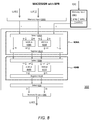
Figure 7 illustrates a block diagram of the execution unit configured to execute an M-width add-sign instruction; and -
Figure 8 illustrates a block diagram of the execution unit configured to execute an M-width add-sign instruction using one or more bit-packed registers. - While the invention is susceptible to various modifications and alternative forms, specific embodiments thereof are shown by way of example in the drawings and are herein described in detail. It should be understood, however, that the drawings and detailed description thereto are not intended to limit the invention to the particular form disclosed, but on the contrary, the intention is to cover all modifications, equivalents and alternatives falling within the scope of the present invention as defined by the appended claims.
- The following publications are relevant:
- R. Gallager, "Low-Density Parity-Check Codes," MIT Press, 1963
- E. Arikan, "Channel Polarization: A method for constructing capacity achieving codes for symmetric binary-input memoryless channels," IEEE Trans. on Inf. Theory, vol. 55, no. 7, pp. 3051-3073, Jul. 2009.
-
U.S. Patent No. 7,415,594 titled "Processing System with Interspersed Stall Propagating Processors and Communication Elements" by Doerr et al. -
U.S. Patent No. 8,880,866 titled "Method and system for disabling communication paths in a multiprocessor fabric by setting register values to disable the communication paths specified by a configuration" by Doerr et al. -
U.S. Patent No. 9,430,369 -
U.S. Patent Application No. 15/359,845 titled "Memory Management and Path Sort Techniques in a Polar Code Successive Cancellation List Decoder" by Raza et al. Terms - The following is a glossary of terms used in the present application:
- Memory Medium - Any of various types of memory devices or storage devices. The term "memory medium" is intended to include an installation medium, e.g., a CD-ROM, floppy disks 104, or tape device; a computer system memory or random access memory such as DRAM, DDR RAM, SRAM, EDO RAM, Rambus RAM, etc.; or a nonvolatile memory such as a magnetic media, e.g., a hard drive, optical storage, or ROM, EPROM, FLASH, etc.. The memory medium may comprise other types of memory as well, or combinations thereof. In addition, the memory medium may be located in a first computer in which the programs are executed, and/or may be located in a second different computer which connects to the first computer over a network, such as the Internet. In the latter instance, the second computer may provide program instructions to the first computer for execution. The term "memory medium" may include two or more memory mediums which may reside in different locations, e.g., in different computers that are connected over a network.
- Carrier Medium -a memory medium as described above, as well as a physical transmission medium, such as a bus, network, and/or other physical transmission medium that conveys signals such as electrical or optical signals.
- Programmable Hardware Element - includes various hardware devices comprising multiple programmable function blocks connected via a programmable or hardwired interconnect. Examples include FPGAs (Field Programmable Gate Arrays), PLDs (Programmable Logic Devices), FPOAs (Field Programmable Object Arrays), and CPLDs (Complex PLDs). The programmable function blocks may range from fine grained (combinatorial logic or look up tables) to coarse grained (arithmetic logic units or processor cores). A programmable hardware element may also be referred to as "reconfigurable logic".
- Application Specific Integrated Circuit (ASIC) - this term is intended to have the full breadth of its ordinary meaning. The term ASIC is intended to include an integrated circuit customized for a particular application, rather than a general purpose programmable device, although ASIC may contain programmable processor cores as building blocks. Cell phone cell, MP3 player chip, and many other single-function ICs are examples of ASICs. An ASIC is usually described in a hardware description language such as Verilog or VHDL.
- Program - the term "program" is intended to have the full breadth of its ordinary meaning. The term "program" includes 1) a software program which may be stored in a memory and is executable by a processor or 2) a hardware configuration program useable for configuring a programmable hardware element or ASIC.
- Software Program - the term "software program" is intended to have the full breadth of its ordinary meaning, and includes any type of program instructions, code, script and/or data, or combinations thereof, that may be stored in a memory medium and executed by a processor. Exemplary software programs include programs written in text-based programming languages, e.g., imperative or procedural languages, such as C, C++, PASCAL, FORTRAN, COBOL, JAVA, assembly language, etc.; graphical programs (programs written in graphical programming languages); assembly language programs; programs that have been compiled to machine language; scripts; and other types of executable software. A software program may comprise two or more software programs that interoperate in some manner.
- Hardware Configuration Program - a program, e.g., a netlist or bit file, that can be used to program or configure a programmable hardware element or ASIC.
- Computer System - any of various types of computing or processing systems, including a personal computer system (PC), mainframe computer system, workstation, network appliance, Internet appliance, personal digital assistant (PDA), grid computing system, or other device or combinations of devices. In general, the term "computer system" can be broadly defined to encompass any device (or combination of devices) having at least one processor that executes instructions from a memory medium.
- Automatically - refers to an action or operation performed by a computer system (e.g., software executed by the computer system) or device (e.g., circuitry, programmable hardware elements, ASICs, etc.), without user input directly specifying or performing the action or operation. Thus the term "automatically" is in contrast to an operation being manually performed or specified by the user, where the user provides input to directly perform the operation. An automatic procedure may be initiated by input provided by the user, but the subsequent actions that are performed "automatically" are not specified by the user, i.e., are not performed "manually", where the user specifies each action to perform. For example, a user filling out an electronic form by selecting each field and providing input specifying information (e.g., by typing information, selecting check boxes, radio selections, etc.) is filling out the form manually, even though the computer system must update the form in response to the user actions. The form may be automatically filled out by the computer system where the computer system (e.g., software executing on the computer system) analyzes the fields of the form and fills in the form without any user input specifying the answers to the fields. As indicated above, the user may invoke the automatic filling of the form, but is not involved in the actual filling of the form (e.g., the user is not manually specifying answers to fields but rather they are being automatically completed). The present specification provides various examples of operations being automatically performed in response to actions the user has taken.
-
Figure 1 shows an example communication system involving abase station 10 communicating with awireless communication device 12. Thebase station 10 may be a cellular base station which performs cellular communications with a plurality of wireless communication devices. Alternatively, thebase station 10 may be a wireless access point for performing Wi-Fi communications, such as according to the 802.11 standard or related standards. Thewireless communication device 12 may be any of various devices such as a smart phone, tablet device, computer system, etc. One or both of thebase station 10 and thewireless communication device 12 may include decoder logic as described herein. -
Figure 2 illustrates an example multi-processor system (MPS) that may be contained in one or both of thebase station 10 and/or thewireless communication device 12. The MPS may be programmed to implement methods described herein. For more information on example MPS architectures which may be used in some embodiments, please seeUS Patent Nos. 7,415,594 and8,880,866 and9,430,369 - In the embodiment illustrated in
Figure 2 , the MPS may include a plurality of processor elements (PEs) (shown as rectangles) and a plurality of data memory routers (DMRs) (shown as circles), which may also be referred to as dynamically configurable communicators, or dynamically configurable communication elements, coupled to communicate data and instructions with each other. As used herein, a PE may also be referred to as a PE node, and a DMR may also be referred to as a DMR node. - The MPS may be used in any of various systems and applications where GPMCs, DSPs, FPGAs, or ASICs are currently used. Thus, for example, the processing system may be used in any of various types of computer systems or other devices that require computation. In one contemplated embodiment, the processing system is used as a signal processing device in an FEC encoder and/or decoder.
- In one embodiment, a PE may include one or more arithmetic-logic units (ALUs) configured for manipulating data, one or more instruction processing units (IPUs) configured for controlling the ALUs, one or more memories configured to hold instructions or data, and multiplexers and decoders of various sorts. Such an embodiment may include a number of ports ("processor ports"), some of which may be configured for connection to DMRs and others that may be configured for connection to other PEs.
- In one embodiment, a DMR may include one or more random access memories (RAMs) configured to hold data and instructions, a configurable controller, a network switch such as a crossbar switch, registers, and multiplexers. Such an embodiment may include a plurality of ports, some of which may be configured for connection to PEs (referred to herein as PE-type ports) and others that may be configured to connect to DMRs (referred to herein as DMR-type ports). It is noted that for any given port, whether configured for connection to or from a DMR or PE, the amount of data transferable through such a given port in a particular clock cycle may vary in various embodiments. For example, in one embodiment, a given port may be configured to transfer one word of data per clock cycle, whereas in another embodiment a given port may be configured to transfer multiple words of data per clock cycle. In yet another embodiment, a given port may employ a technique such as time-division multiplexing to transfer one word of data over multiple clock cycles, thereby reducing the number of physical connections comprising the port.
- In one embodiment of the MPS, each PE may include a small local memory reserved for instructions and may include very little local data storage. In such an embodiment, DMRs neighboring each PE may be configured to provide operands to a given PE. In a particular embodiment, for many PE instructions a given PE may read operands from neighboring DMRs, execute an ALU operation, and store an ALU result to a given neighboring DMR in one clock cycle. An ALU result from one PE may thereby be made available to several other PEs in the clock cycle immediately following execution. Producing results in this fashion may enable the execution of neighboring PEs to be closely coordinated or "tightly coupled." In other embodiments, each PE may include additional registers for buffering operands and/or result data.
- In one embodiment of the MPS, data and instructions may be transferred among the DMRs in one of several different ways. A serial bus may be provided to all memories in the MPS; such a bus may be used to initialize the MPS from external memory or to support testing of MPS data structures. For short-distance transfers, a given PE may be programmed to directly move data to or from its neighbor DMRs. To transfer data or instructions over longer distances, communication pathways may be dynamically created and destroyed in the network of DMRs. For the purpose of such longer-distance data transfer, a network of interconnected DMRs within the MPS may constitute a switched routing fabric (SRF) for communication pathways.
- To prevent potential loss of data words on a pathway, an embodiment of
MPS 10 may implement flow control between receivers and transmitters along the pathway. Flow control refers to a mechanism that may stop a transmitter if its corresponding receiver can no longer receive data, and may restart a transmitter when its corresponding receiver becomes ready to receive data. Because stopping and restarting the flow of data on a pathway has many similarities to stopping and restarting the progress of a message in wormhole routing, the two may be combined in an integrated scheme. - In one embodiment, the MPS may include pluralities of PEs and DMRs, which PEs may be identical and which DMRs may be identical, connected together in a uniform array. In a uniform array, the majority of PEs may be identical and each of a majority of PEs may have the same number of connections to DMRs. Also, in a uniform array, the majority of DMRs may be identical and each of a majority of DMRs may have the same number of connections to other DMRs and to PEs. The PEs and DMRs in one MPS embodiment may be interspersed in a substantially homogeneous fashion. As used herein, a substantially homogeneous interspersion refers to an arrangement in which the ratio of PEs to DMRs is consistent across a majority of sub-regions of an array.
- A uniform array arranged in a substantially homogeneous fashion may have certain advantageous characteristics, such as providing a predictable interconnection pattern and enabling software modules to be re-used across the array. In one embodiment, a uniform array may enable a small number of instances of PEs and DMRs to be designed and tested. A system may then be assembled by fabricating a unit comprising a DMR and a PE and then repeating or "tiling" such a unit multiple times. Such an approach may lower design and test costs through reuse of common system elements.
- It is also noted that the configurable nature of the PE and DMR may allow a great variety of non-uniform behavior to be programmed to occur on a physically uniform array. However, in an alternative embodiment, the MPS may also be formed with non-uniform DMR and PE units, which may be connected in a regular or irregular array, or even in a random way. In one embodiment, PE and DMR interconnections may be implemented as circuit traces, for example on an integrated circuit (IC), ceramic substrate, or printed circuit board (PCB). However, in alternative embodiments, such interconnections may be any of a variety of miniature communication links, such as waveguides for electromagnetic energy (i.e., radio or optical energy), wireless (i.e., unguided) energy, particles (such as electron beams), or potentials on molecules, for example.
- The MPS may be implemented on a single integrated circuit. In one embodiment, a plurality of MPS integrated circuits may be combined to produce a larger system. However, alternative MPS embodiments are contemplated that include different arrangements of PEs and DMRs
- In some embodiments, the MPS may employ the best features of DSP and FPGA architectures. Like a DSP, the MPS may be a programmable chip with multiple processing units and on-chip memory. However, relative to a DSP, the MPS processing units may be streamlined, there may be more of them, and they may be interconnected in a novel way to maximize the bandwidth of data movement between them as well as data movement on and off the chip. Having more processing units than a DSP may allow the MPS to do more processes per unit time, and streamlined processing units may minimize energy use. Many DSPs with internal parallelism may be bus-oriented architectures. In some embodiments, the MPS may not include a bus, but rather may include neighboring shared local memories, such as in a DMR, embedded in an SRF that may provide significantly higher total bandwidth than a bus-oriented architecture.
- Compared to the FPGA approach, some MPS embodiments may be more coarsely grained. For example, in one MPS embodiment, operations may have a natural word length (e.g., 16-bits) and computation may be most efficient if performed using data that is a multiple of the natural word length. In some MPS embodiments, PEs and DMRs may be denser than the equivalent structures realized in FPGA, which may result in shorter average wiring length, lower wiring capacitance and less energy use. In contrast to an FPGA implementation, in some MPS embodiments, every ALU in the MPS may be part of a processor (i.e., a PE), which may facilitate the fetch of operands and the write back of results to surrounding fast memory in the DMRs. Timing and clock skew issues for ALU, fetch, and write back operations may be solved once during the design of the IC chip and need not be re-solved with each new application as is typical of FPGA implementations.
- As noted above, the MPS of
Figure 2 may be used as a signal processing device in an FEC encoder and/or decoder. Various schemes for performing FEC encoding and decoding may involve the following operations:

- In equations 1 and 2, each of "x" and "y" are numbers (negative, positive, or zero), while "u" has a value of either zero or one.
- The function extsign(a) extracts the sign of "a", which, in some scenarios, may be returned as a result in the set of [-1, 0, +1]. In other scenarios, the result may instead be limited to the set of [-1, +1] or [-1, 0]. In other scenarios, an alternative sign representation may be used.
- The function min(a, b) returns the minimum value between the values "a" and "b".
- The function sat(a) returns a "saturated" value of "a", based on a pre-defined minimum value "MIN_VAL" and a maximum value "MAX_VAL" (where MIN_VAL < MAX_VAL) as follows:
       if a < MIN_VAL, then sat(a) = MIN_VAL
       if a > MAX_VAL, then sat(a) = MAX_VAL
       if MIN VAL <= a <= MAX VAL, then sat(a) = a
       if sign_xy > 0 (e.g., +1), then Z = min_xy
       if sign_xy = 0, then Z = 0
       if sign_xy < 0 (e.g., -1), then Z = -min_xy
       if sign_xy = -1, then Z = -min_xy
       if sign_xy ≠ -1, then Z = min_xy
Claims (10)
- A processing element (300), comprising:
a data-processing pathway configured to execute a first instruction that specifies a first input operand and a second input operand, wherein, in executing the first instruction, the processing element is configured to:determine an absolute value and a sign function of the first input operand;determine an absolute value and a sign function of the second input operand;determine a minimum magnitude value comprising a minimum of the absolute value of the first input operand and the absolute value of the second input operand;determine a final sign function comprising a product of the sign function of the first input value and the sign function of the second input value; andapply the final sign function to the minimum magnitude value, wherein the result of applying the final sign function to the minimum magnitude value constitutes a result value for the first input operand and the second input operand. - The processing element of claim 1, wherein the first instruction specifies the first input operand by specifying a memory location at which the first input operand is located, and wherein the first instruction specifies the second input operand by specifying a memory location at which the second input operand is located.
- The processing element of claim 1, wherein the first instruction further specifies a plural set of first input operands and a plural set of second input operands, wherein, in executing the first instruction, the processing element is configured to produce a plural set of result values for the plural set of first input operands and the plural set of second input operands.
- The processing element of claim 1, wherein the data-processing pathway comprises a first data-processing pathway, the processing element further comprising:
a second data-processing pathway, wherein the second data-processing pathway is configured in the same manner as the first data-processing pathway. - The processing element of claim 1,wherein the data-processing pathway comprises a plurality of pipelined operational stages, each operational stage configurable to perform a plurality of data processing operations;wherein the processing element is configured to, in response to receiving the first instruction:configure a first operational stage of the plurality of pipelined operational stages to perform the determining the absolute value and the sign function of the first input operand and the determining the absolute value and the sign function of the second input operand;configure a second operational stage of the plurality of pipelined operational stages to perform the determining the minimum magnitude value and the determining the final sign function; andconfigure a third operational stage of the plurality of pipelined operational stages to perform the applying the final sign function.
- The processing element of claim 5, wherein:the first operational stage is configured to determine the absolute value and the sign function of the first input operand, and determine the absolute value and the sign function of the second input operand during a first clock cycle;the second operational stage is configured to determine the minimum magnitude value and determine final sign function during a second clock cycle; andthe third operational stage is configured to apply the final sign function to the minimum magnitude value during a third clock cycle.
- The processing element of claim 6, further configured to, in response to receiving the first instruction, sequentially process a plurality of pairs of input operands, wherein the first input operand and the second input operand constitute a first pair of the plurality of pairs of input operands;
wherein the first operational stage is configured to determine an absolute value and a sign of each input operand of a respective pair of input operands during each clock cycle of a plurality of consecutive clock cycles. - The processing element of claim 5, further configured to, in response to receiving a second, different instruction, configure at least one operational stage to perform a plurality of data-processing operations other than those configured in response to receiving the first instruction.
- The processing element of claim 5, wherein the plurality of pipelined operational stages comprises a first plurality of pipelined operational stages, the processing element further comprising:
a second plurality of pipelined operational stages, wherein the second plurality of pipelined operational stages are configured in the same manner as the first plurality of pipelined operational stages. - The processing elements of clam 5, wherein configuring an operational stage comprises selecting a plurality of data-processing operations to be performed by the operational stage, and selecting registers from which inputs to the selected data-processing operations will be provided.
Priority Applications (1)
| Application Number | Priority Date | Filing Date | Title |
|---|---|---|---|
| EP20161395.7A EP3686735B1 (en) | 2015-12-28 | 2016-12-27 | Processor instructions to accelerate fec encoding and decoding |
Applications Claiming Priority (2)
| Application Number | Priority Date | Filing Date | Title |
|---|---|---|---|
| US201562271578P | 2015-12-28 | 2015-12-28 | |
| PCT/US2016/068692 WO2017117116A1 (en) | 2015-12-28 | 2016-12-27 | Processor Instructions to Accelerate FEC Encoding and Decoding |
Related Child Applications (1)
| Application Number | Title | Priority Date | Filing Date |
|---|---|---|---|
| EP20161395.7A Division EP3686735B1 (en) | 2015-12-28 | 2016-12-27 | Processor instructions to accelerate fec encoding and decoding |
Publications (2)
| Publication Number | Publication Date |
|---|---|
| EP3398053A1 EP3398053A1 (en) | 2018-11-07 |
| EP3398053B1 true EP3398053B1 (en) | 2020-03-25 |
Family
ID=57822083
Family Applications (2)
| Application Number | Title | Priority Date | Filing Date |
|---|---|---|---|
| EP20161395.7A Active EP3686735B1 (en) | 2015-12-28 | 2016-12-27 | Processor instructions to accelerate fec encoding and decoding |
| EP16826852.2A Active EP3398053B1 (en) | 2015-12-28 | 2016-12-27 | Processor instructions to accelerate fec encoding and decoding |
Family Applications Before (1)
| Application Number | Title | Priority Date | Filing Date |
|---|---|---|---|
| EP20161395.7A Active EP3686735B1 (en) | 2015-12-28 | 2016-12-27 | Processor instructions to accelerate fec encoding and decoding |
Country Status (5)
| Country | Link |
|---|---|
| US (2) | US10691451B2 (en) |
| EP (2) | EP3686735B1 (en) |
| JP (1) | JP6933648B2 (en) |
| CN (1) | CN108701021B (en) |
| WO (1) | WO2017117116A1 (en) |
Family Cites Families (16)
| Publication number | Priority date | Publication date | Assignee | Title |
|---|---|---|---|---|
| US4589067A (en) | 1983-05-27 | 1986-05-13 | Analogic Corporation | Full floating point vector processor with dynamically configurable multifunction pipelined ALU |
| JP3672076B2 (en) * | 1999-09-22 | 2005-07-13 | 松下電器産業株式会社 | Operation unit, operation method, and processor |
| US6922716B2 (en) * | 2001-07-13 | 2005-07-26 | Motorola, Inc. | Method and apparatus for vector processing |
| US7937559B1 (en) * | 2002-05-13 | 2011-05-03 | Tensilica, Inc. | System and method for generating a configurable processor supporting a user-defined plurality of instruction sizes |
| KR100891782B1 (en) * | 2002-06-11 | 2009-04-07 | 삼성전자주식회사 | Apparatus and method for correcting of forward error in high data transmission system |
| US7415594B2 (en) | 2002-06-26 | 2008-08-19 | Coherent Logix, Incorporated | Processing system with interspersed stall propagating processors and communication elements |
| US20080281897A1 (en) * | 2007-05-07 | 2008-11-13 | Messinger Daaven S | Universal execution unit |
| US20090113174A1 (en) * | 2007-10-31 | 2009-04-30 | Texas Instruments Incorporated | Sign Operation Instructions and Circuitry |
| US9152427B2 (en) * | 2008-10-15 | 2015-10-06 | Hyperion Core, Inc. | Instruction issue to array of arithmetic cells coupled to load/store cells with associated registers as extended register file |
| JP2011028543A (en) * | 2009-07-27 | 2011-02-10 | Renesas Electronics Corp | Information processing system, and information processing method for the same |
| CN103154925B (en) | 2010-10-15 | 2016-08-24 | 相干逻辑公司 | Communication disabling in multicomputer system |
| WO2012093288A1 (en) * | 2011-01-03 | 2012-07-12 | Freescale Semiconductor, Inc. | Integrated circuit device and method for performing conditional negation of data |
| US9176927B2 (en) * | 2011-11-08 | 2015-11-03 | The Royal Institution For The Advancement Of Learning/Mcgill University | Methods and systems for decoding polar codes |
| US9904542B2 (en) * | 2012-11-06 | 2018-02-27 | Coherent Logix, Incorporated | Multiprocessor programming toolkit for design reuse |
| JP2016526220A (en) * | 2013-05-24 | 2016-09-01 | コーヒレント・ロジックス・インコーポレーテッド | Memory network processor with programmable optimization |
| EP3033862A1 (en) * | 2013-08-16 | 2016-06-22 | Origin Wireless, Inc. | Time-reversal wireless systems having asymmetric architecture |
-
2016
- 2016-12-27 US US15/390,910 patent/US10691451B2/en active Active
- 2016-12-27 WO PCT/US2016/068692 patent/WO2017117116A1/en active Application Filing
- 2016-12-27 CN CN201680080836.4A patent/CN108701021B/en active Active
- 2016-12-27 JP JP2018534109A patent/JP6933648B2/en active Active
- 2016-12-27 EP EP20161395.7A patent/EP3686735B1/en active Active
- 2016-12-27 EP EP16826852.2A patent/EP3398053B1/en active Active
-
2020
- 2020-06-22 US US16/907,715 patent/US11327753B2/en active Active
Non-Patent Citations (1)
| Title |
|---|
| None * |
Also Published As
| Publication number | Publication date |
|---|---|
| CN108701021A (en) | 2018-10-23 |
| JP2019508785A (en) | 2019-03-28 |
| EP3686735B1 (en) | 2022-05-04 |
| US11327753B2 (en) | 2022-05-10 |
| US10691451B2 (en) | 2020-06-23 |
| EP3398053A1 (en) | 2018-11-07 |
| US20170185399A1 (en) | 2017-06-29 |
| CN108701021B (en) | 2023-06-09 |
| US20200319880A1 (en) | 2020-10-08 |
| JP6933648B2 (en) | 2021-09-08 |
| WO2017117116A1 (en) | 2017-07-06 |
| EP3686735A1 (en) | 2020-07-29 |
Similar Documents
| Publication | Publication Date | Title |
|---|---|---|
| US20090300336A1 (en) | Microprocessor with highly configurable pipeline and executional unit internal hierarchal structures, optimizable for different types of computational functions | |
| WO2019218896A1 (en) | Computing method and related product | |
| Grymel et al. | A novel programmable parallel CRC circuit | |
| US11321096B2 (en) | Hardware unit for performing matrix multiplication with clock gating | |
| CN110716707A (en) | Prefix network directed addition | |
| US11327753B2 (en) | Processor instructions to accelerate FEC encoding and decoding | |
| US10484021B1 (en) | Log-likelihood ratio processing for linear block code decoding | |
| US10691416B2 (en) | Performing constant modulo arithmetic | |
| US11704535B1 (en) | Hardware architecture for a neural network accelerator | |
| US10387155B2 (en) | Controlling register bank access between program and dedicated processors in a processing system | |
| US7007059B1 (en) | Fast pipelined adder/subtractor using increment/decrement function with reduced register utilization | |
| EP3089027B1 (en) | Simd processing module | |
| Chen et al. | PipeCIM: A High-Throughput Computing-In-Memory Microprocessor With Nested Pipeline and RISC-V Extended Instructions | |
| Corsonello et al. | Variable precision multipliers for FPGA-based reconfigurable computing systems | |
| Zhang et al. | R-LDPC: Refining Behavior Descriptions in HLS to Implement High-throughput LDPC Decoder | |
| KR20240037146A (en) | Multi-bit accumulator, in memory computing(imc) processor including multi-bit accumulator, and operating method of multi-bit accumulator | |
| Sunitha et al. | Design and Comparison of Risc Processors Using Different Alu Architectures | |
| CN115168284A (en) | Coarse-grained reconfigurable array system and calculation method for deep learning | |
| Kesler et al. | Design and verification of dynamically reconfigurable architecture | |
| GB2584228A (en) | Hardware unit for performing matrix multiplication with clock gating | |
| CN114218524A (en) | Large-scale multi-operation floating-point matrix calculation acceleration implementation method and device | |
| GB2576282A (en) | Hardware unit for performing matrix multiplication with clock gating | |
| GB2591713A (en) | Hardware unit for performing matrix multiplication with clock gating |
Legal Events
| Date | Code | Title | Description |
|---|---|---|---|
| STAA | Information on the status of an ep patent application or granted ep patent |
Free format text: STATUS: UNKNOWN |
|
| STAA | Information on the status of an ep patent application or granted ep patent |
Free format text: STATUS: THE INTERNATIONAL PUBLICATION HAS BEEN MADE |
|
| PUAI | Public reference made under article 153(3) epc to a published international application that has entered the european phase |
Free format text: ORIGINAL CODE: 0009012 |
|
| STAA | Information on the status of an ep patent application or granted ep patent |
Free format text: STATUS: REQUEST FOR EXAMINATION WAS MADE |
|
| 17P | Request for examination filed |
Effective date: 20180720 |
|
| AK | Designated contracting states |
Kind code of ref document: A1 Designated state(s): AL AT BE BG CH CY CZ DE DK EE ES FI FR GB GR HR HU IE IS IT LI LT LU LV MC MK MT NL NO PL PT RO RS SE SI SK SM TR |
|
| AX | Request for extension of the european patent |
Extension state: BA ME |
|
| DAV | Request for validation of the european patent (deleted) | ||
| DAX | Request for extension of the european patent (deleted) | ||
| GRAP | Despatch of communication of intention to grant a patent |
Free format text: ORIGINAL CODE: EPIDOSNIGR1 |
|
| STAA | Information on the status of an ep patent application or granted ep patent |
Free format text: STATUS: GRANT OF PATENT IS INTENDED |
|
| INTG | Intention to grant announced |
Effective date: 20191014 |
|
| GRAS | Grant fee paid |
Free format text: ORIGINAL CODE: EPIDOSNIGR3 |
|
| GRAA | (expected) grant |
Free format text: ORIGINAL CODE: 0009210 |
|
| STAA | Information on the status of an ep patent application or granted ep patent |
Free format text: STATUS: THE PATENT HAS BEEN GRANTED |
|
| AK | Designated contracting states |
Kind code of ref document: B1 Designated state(s): AL AT BE BG CH CY CZ DE DK EE ES FI FR GB GR HR HU IE IS IT LI LT LU LV MC MK MT NL NO PL PT RO RS SE SI SK SM TR |
|
| REG | Reference to a national code |
Ref country code: GB Ref legal event code: FG4D |
|
| REG | Reference to a national code |
Ref country code: AT Ref legal event code: REF Ref document number: 1249344 Country of ref document: AT Kind code of ref document: T Effective date: 20200415 Ref country code: IE Ref legal event code: FG4D |
|
| REG | Reference to a national code |
Ref country code: DE Ref legal event code: R096 Ref document number: 602016032696 Country of ref document: DE |
|
| PG25 | Lapsed in a contracting state [announced via postgrant information from national office to epo] |
Ref country code: FI Free format text: LAPSE BECAUSE OF FAILURE TO SUBMIT A TRANSLATION OF THE DESCRIPTION OR TO PAY THE FEE WITHIN THE PRESCRIBED TIME-LIMIT Effective date: 20200325 Ref country code: RS Free format text: LAPSE BECAUSE OF FAILURE TO SUBMIT A TRANSLATION OF THE DESCRIPTION OR TO PAY THE FEE WITHIN THE PRESCRIBED TIME-LIMIT Effective date: 20200325 Ref country code: NO Free format text: LAPSE BECAUSE OF FAILURE TO SUBMIT A TRANSLATION OF THE DESCRIPTION OR TO PAY THE FEE WITHIN THE PRESCRIBED TIME-LIMIT Effective date: 20200625 |
|
| PG25 | Lapsed in a contracting state [announced via postgrant information from national office to epo] |
Ref country code: LV Free format text: LAPSE BECAUSE OF FAILURE TO SUBMIT A TRANSLATION OF THE DESCRIPTION OR TO PAY THE FEE WITHIN THE PRESCRIBED TIME-LIMIT Effective date: 20200325 Ref country code: SE Free format text: LAPSE BECAUSE OF FAILURE TO SUBMIT A TRANSLATION OF THE DESCRIPTION OR TO PAY THE FEE WITHIN THE PRESCRIBED TIME-LIMIT Effective date: 20200325 Ref country code: HR Free format text: LAPSE BECAUSE OF FAILURE TO SUBMIT A TRANSLATION OF THE DESCRIPTION OR TO PAY THE FEE WITHIN THE PRESCRIBED TIME-LIMIT Effective date: 20200325 Ref country code: BG Free format text: LAPSE BECAUSE OF FAILURE TO SUBMIT A TRANSLATION OF THE DESCRIPTION OR TO PAY THE FEE WITHIN THE PRESCRIBED TIME-LIMIT Effective date: 20200625 Ref country code: GR Free format text: LAPSE BECAUSE OF FAILURE TO SUBMIT A TRANSLATION OF THE DESCRIPTION OR TO PAY THE FEE WITHIN THE PRESCRIBED TIME-LIMIT Effective date: 20200626 |
|
| REG | Reference to a national code |
Ref country code: NL Ref legal event code: MP Effective date: 20200325 |
|
| REG | Reference to a national code |
Ref country code: LT Ref legal event code: MG4D |
|
| PG25 | Lapsed in a contracting state [announced via postgrant information from national office to epo] |
Ref country code: NL Free format text: LAPSE BECAUSE OF FAILURE TO SUBMIT A TRANSLATION OF THE DESCRIPTION OR TO PAY THE FEE WITHIN THE PRESCRIBED TIME-LIMIT Effective date: 20200325 |
|
| PG25 | Lapsed in a contracting state [announced via postgrant information from national office to epo] |
Ref country code: EE Free format text: LAPSE BECAUSE OF FAILURE TO SUBMIT A TRANSLATION OF THE DESCRIPTION OR TO PAY THE FEE WITHIN THE PRESCRIBED TIME-LIMIT Effective date: 20200325 Ref country code: RO Free format text: LAPSE BECAUSE OF FAILURE TO SUBMIT A TRANSLATION OF THE DESCRIPTION OR TO PAY THE FEE WITHIN THE PRESCRIBED TIME-LIMIT Effective date: 20200325 Ref country code: CZ Free format text: LAPSE BECAUSE OF FAILURE TO SUBMIT A TRANSLATION OF THE DESCRIPTION OR TO PAY THE FEE WITHIN THE PRESCRIBED TIME-LIMIT Effective date: 20200325 Ref country code: LT Free format text: LAPSE BECAUSE OF FAILURE TO SUBMIT A TRANSLATION OF THE DESCRIPTION OR TO PAY THE FEE WITHIN THE PRESCRIBED TIME-LIMIT Effective date: 20200325 Ref country code: SM Free format text: LAPSE BECAUSE OF FAILURE TO SUBMIT A TRANSLATION OF THE DESCRIPTION OR TO PAY THE FEE WITHIN THE PRESCRIBED TIME-LIMIT Effective date: 20200325 Ref country code: SK Free format text: LAPSE BECAUSE OF FAILURE TO SUBMIT A TRANSLATION OF THE DESCRIPTION OR TO PAY THE FEE WITHIN THE PRESCRIBED TIME-LIMIT Effective date: 20200325 Ref country code: PT Free format text: LAPSE BECAUSE OF FAILURE TO SUBMIT A TRANSLATION OF THE DESCRIPTION OR TO PAY THE FEE WITHIN THE PRESCRIBED TIME-LIMIT Effective date: 20200818 Ref country code: IS Free format text: LAPSE BECAUSE OF FAILURE TO SUBMIT A TRANSLATION OF THE DESCRIPTION OR TO PAY THE FEE WITHIN THE PRESCRIBED TIME-LIMIT Effective date: 20200725 |
|
| REG | Reference to a national code |
Ref country code: AT Ref legal event code: MK05 Ref document number: 1249344 Country of ref document: AT Kind code of ref document: T Effective date: 20200325 |
|
| REG | Reference to a national code |
Ref country code: DE Ref legal event code: R097 Ref document number: 602016032696 Country of ref document: DE |
|
| PG25 | Lapsed in a contracting state [announced via postgrant information from national office to epo] |
Ref country code: AT Free format text: LAPSE BECAUSE OF FAILURE TO SUBMIT A TRANSLATION OF THE DESCRIPTION OR TO PAY THE FEE WITHIN THE PRESCRIBED TIME-LIMIT Effective date: 20200325 Ref country code: IT Free format text: LAPSE BECAUSE OF FAILURE TO SUBMIT A TRANSLATION OF THE DESCRIPTION OR TO PAY THE FEE WITHIN THE PRESCRIBED TIME-LIMIT Effective date: 20200325 Ref country code: ES Free format text: LAPSE BECAUSE OF FAILURE TO SUBMIT A TRANSLATION OF THE DESCRIPTION OR TO PAY THE FEE WITHIN THE PRESCRIBED TIME-LIMIT Effective date: 20200325 Ref country code: DK Free format text: LAPSE BECAUSE OF FAILURE TO SUBMIT A TRANSLATION OF THE DESCRIPTION OR TO PAY THE FEE WITHIN THE PRESCRIBED TIME-LIMIT Effective date: 20200325 |
|
| PLBE | No opposition filed within time limit |
Free format text: ORIGINAL CODE: 0009261 |
|
| STAA | Information on the status of an ep patent application or granted ep patent |
Free format text: STATUS: NO OPPOSITION FILED WITHIN TIME LIMIT |
|
| PG25 | Lapsed in a contracting state [announced via postgrant information from national office to epo] |
Ref country code: PL Free format text: LAPSE BECAUSE OF FAILURE TO SUBMIT A TRANSLATION OF THE DESCRIPTION OR TO PAY THE FEE WITHIN THE PRESCRIBED TIME-LIMIT Effective date: 20200325 |
|
| 26N | No opposition filed |
Effective date: 20210112 |
|
| PG25 | Lapsed in a contracting state [announced via postgrant information from national office to epo] |
Ref country code: SI Free format text: LAPSE BECAUSE OF FAILURE TO SUBMIT A TRANSLATION OF THE DESCRIPTION OR TO PAY THE FEE WITHIN THE PRESCRIBED TIME-LIMIT Effective date: 20200325 |
|
| REG | Reference to a national code |
Ref country code: CH Ref legal event code: PL |
|
| PG25 | Lapsed in a contracting state [announced via postgrant information from national office to epo] |
Ref country code: MC Free format text: LAPSE BECAUSE OF FAILURE TO SUBMIT A TRANSLATION OF THE DESCRIPTION OR TO PAY THE FEE WITHIN THE PRESCRIBED TIME-LIMIT Effective date: 20200325 |
|
| REG | Reference to a national code |
Ref country code: BE Ref legal event code: MM Effective date: 20201231 |
|
| PG25 | Lapsed in a contracting state [announced via postgrant information from national office to epo] |
Ref country code: LU Free format text: LAPSE BECAUSE OF NON-PAYMENT OF DUE FEES Effective date: 20201227 Ref country code: IE Free format text: LAPSE BECAUSE OF NON-PAYMENT OF DUE FEES Effective date: 20201227 |
|
| PG25 | Lapsed in a contracting state [announced via postgrant information from national office to epo] |
Ref country code: CH Free format text: LAPSE BECAUSE OF NON-PAYMENT OF DUE FEES Effective date: 20201231 Ref country code: LI Free format text: LAPSE BECAUSE OF NON-PAYMENT OF DUE FEES Effective date: 20201231 |
|
| PG25 | Lapsed in a contracting state [announced via postgrant information from national office to epo] |
Ref country code: TR Free format text: LAPSE BECAUSE OF FAILURE TO SUBMIT A TRANSLATION OF THE DESCRIPTION OR TO PAY THE FEE WITHIN THE PRESCRIBED TIME-LIMIT Effective date: 20200325 Ref country code: MT Free format text: LAPSE BECAUSE OF FAILURE TO SUBMIT A TRANSLATION OF THE DESCRIPTION OR TO PAY THE FEE WITHIN THE PRESCRIBED TIME-LIMIT Effective date: 20200325 Ref country code: CY Free format text: LAPSE BECAUSE OF FAILURE TO SUBMIT A TRANSLATION OF THE DESCRIPTION OR TO PAY THE FEE WITHIN THE PRESCRIBED TIME-LIMIT Effective date: 20200325 |
|
| PG25 | Lapsed in a contracting state [announced via postgrant information from national office to epo] |
Ref country code: MK Free format text: LAPSE BECAUSE OF FAILURE TO SUBMIT A TRANSLATION OF THE DESCRIPTION OR TO PAY THE FEE WITHIN THE PRESCRIBED TIME-LIMIT Effective date: 20200325 Ref country code: AL Free format text: LAPSE BECAUSE OF FAILURE TO SUBMIT A TRANSLATION OF THE DESCRIPTION OR TO PAY THE FEE WITHIN THE PRESCRIBED TIME-LIMIT Effective date: 20200325 |
|
| PG25 | Lapsed in a contracting state [announced via postgrant information from national office to epo] |
Ref country code: BE Free format text: LAPSE BECAUSE OF NON-PAYMENT OF DUE FEES Effective date: 20201231 |
|
| PGFP | Annual fee paid to national office [announced via postgrant information from national office to epo] |
Ref country code: FR Payment date: 20230526 Year of fee payment: 7 Ref country code: DE Payment date: 20230530 Year of fee payment: 7 |
|
| PGFP | Annual fee paid to national office [announced via postgrant information from national office to epo] |
Ref country code: GB Payment date: 20230529 Year of fee payment: 7 |