EP3396505A1 - Display screen, display device and mobile terminal - Google Patents
Display screen, display device and mobile terminal Download PDFInfo
- Publication number
- EP3396505A1 EP3396505A1 EP17210894.6A EP17210894A EP3396505A1 EP 3396505 A1 EP3396505 A1 EP 3396505A1 EP 17210894 A EP17210894 A EP 17210894A EP 3396505 A1 EP3396505 A1 EP 3396505A1
- Authority
- EP
- European Patent Office
- Prior art keywords
- light
- layer
- hole
- display
- display screen
- Prior art date
- Legal status (The legal status is an assumption and is not a legal conclusion. Google has not performed a legal analysis and makes no representation as to the accuracy of the status listed.)
- Granted
Links
Images



Classifications
-
- G—PHYSICS
- G06—COMPUTING OR CALCULATING; COUNTING
- G06F—ELECTRIC DIGITAL DATA PROCESSING
- G06F1/00—Details not covered by groups G06F3/00 - G06F13/00 and G06F21/00
- G06F1/16—Constructional details or arrangements
- G06F1/1613—Constructional details or arrangements for portable computers
- G06F1/1633—Constructional details or arrangements of portable computers not specific to the type of enclosures covered by groups G06F1/1615 - G06F1/1626
- G06F1/1637—Details related to the display arrangement, including those related to the mounting of the display in the housing
-
- G—PHYSICS
- G06—COMPUTING OR CALCULATING; COUNTING
- G06F—ELECTRIC DIGITAL DATA PROCESSING
- G06F1/00—Details not covered by groups G06F3/00 - G06F13/00 and G06F21/00
- G06F1/16—Constructional details or arrangements
- G06F1/1613—Constructional details or arrangements for portable computers
- G06F1/1633—Constructional details or arrangements of portable computers not specific to the type of enclosures covered by groups G06F1/1615 - G06F1/1626
- G06F1/1684—Constructional details or arrangements related to integrated I/O peripherals not covered by groups G06F1/1635 - G06F1/1675
-
- G—PHYSICS
- G06—COMPUTING OR CALCULATING; COUNTING
- G06F—ELECTRIC DIGITAL DATA PROCESSING
- G06F3/00—Input arrangements for transferring data to be processed into a form capable of being handled by the computer; Output arrangements for transferring data from processing unit to output unit, e.g. interface arrangements
- G06F3/01—Input arrangements or combined input and output arrangements for interaction between user and computer
- G06F3/03—Arrangements for converting the position or the displacement of a member into a coded form
- G06F3/041—Digitisers, e.g. for touch screens or touch pads, characterised by the transducing means
- G06F3/0412—Digitisers structurally integrated in a display
-
- G—PHYSICS
- G06—COMPUTING OR CALCULATING; COUNTING
- G06F—ELECTRIC DIGITAL DATA PROCESSING
- G06F3/00—Input arrangements for transferring data to be processed into a form capable of being handled by the computer; Output arrangements for transferring data from processing unit to output unit, e.g. interface arrangements
- G06F3/01—Input arrangements or combined input and output arrangements for interaction between user and computer
- G06F3/03—Arrangements for converting the position or the displacement of a member into a coded form
- G06F3/041—Digitisers, e.g. for touch screens or touch pads, characterised by the transducing means
- G06F3/042—Digitisers, e.g. for touch screens or touch pads, characterised by the transducing means by opto-electronic means
-
- G—PHYSICS
- G06—COMPUTING OR CALCULATING; COUNTING
- G06V—IMAGE OR VIDEO RECOGNITION OR UNDERSTANDING
- G06V40/00—Recognition of biometric, human-related or animal-related patterns in image or video data
- G06V40/10—Human or animal bodies, e.g. vehicle occupants or pedestrians; Body parts, e.g. hands
- G06V40/12—Fingerprints or palmprints
- G06V40/13—Sensors therefor
-
- G—PHYSICS
- G06—COMPUTING OR CALCULATING; COUNTING
- G06V—IMAGE OR VIDEO RECOGNITION OR UNDERSTANDING
- G06V40/00—Recognition of biometric, human-related or animal-related patterns in image or video data
- G06V40/10—Human or animal bodies, e.g. vehicle occupants or pedestrians; Body parts, e.g. hands
- G06V40/12—Fingerprints or palmprints
- G06V40/13—Sensors therefor
- G06V40/1306—Sensors therefor non-optical, e.g. ultrasonic or capacitive sensing
-
- G—PHYSICS
- G06—COMPUTING OR CALCULATING; COUNTING
- G06V—IMAGE OR VIDEO RECOGNITION OR UNDERSTANDING
- G06V40/00—Recognition of biometric, human-related or animal-related patterns in image or video data
- G06V40/10—Human or animal bodies, e.g. vehicle occupants or pedestrians; Body parts, e.g. hands
- G06V40/12—Fingerprints or palmprints
- G06V40/13—Sensors therefor
- G06V40/1318—Sensors therefor using electro-optical elements or layers, e.g. electroluminescent sensing
-
- G—PHYSICS
- G02—OPTICS
- G02F—OPTICAL DEVICES OR ARRANGEMENTS FOR THE CONTROL OF LIGHT BY MODIFICATION OF THE OPTICAL PROPERTIES OF THE MEDIA OF THE ELEMENTS INVOLVED THEREIN; NON-LINEAR OPTICS; FREQUENCY-CHANGING OF LIGHT; OPTICAL LOGIC ELEMENTS; OPTICAL ANALOGUE/DIGITAL CONVERTERS
- G02F1/00—Devices or arrangements for the control of the intensity, colour, phase, polarisation or direction of light arriving from an independent light source, e.g. switching, gating or modulating; Non-linear optics
- G02F1/01—Devices or arrangements for the control of the intensity, colour, phase, polarisation or direction of light arriving from an independent light source, e.g. switching, gating or modulating; Non-linear optics for the control of the intensity, phase, polarisation or colour
- G02F1/13—Devices or arrangements for the control of the intensity, colour, phase, polarisation or direction of light arriving from an independent light source, e.g. switching, gating or modulating; Non-linear optics for the control of the intensity, phase, polarisation or colour based on liquid crystals, e.g. single liquid crystal display cells
- G02F1/133—Constructional arrangements; Operation of liquid crystal cells; Circuit arrangements
- G02F1/1333—Constructional arrangements; Manufacturing methods
- G02F1/1335—Structural association of cells with optical devices, e.g. polarisers or reflectors
- G02F1/133509—Filters, e.g. light shielding masks
- G02F1/133512—Light shielding layers, e.g. black matrix
-
- H—ELECTRICITY
- H10—SEMICONDUCTOR DEVICES; ELECTRIC SOLID-STATE DEVICES NOT OTHERWISE PROVIDED FOR
- H10K—ORGANIC ELECTRIC SOLID-STATE DEVICES
- H10K59/00—Integrated devices, or assemblies of multiple devices, comprising at least one organic light-emitting element covered by group H10K50/00
- H10K59/10—OLED displays
- H10K59/12—Active-matrix OLED [AMOLED] displays
- H10K59/126—Shielding, e.g. light-blocking means over the TFTs
Definitions
- the present disclosure relates to a field of electronic apparatus, and particularly to a display screen, a display device and a mobile terminal.
- fingerprint recognition unit is disposed outside a display area of a display panel so as to be prevented from hindering display.
- a display area-to-screen ratio (a ratio of the display area to the whole display screen) is low.
- the display area-to-screen ratio can be increased by disposing a fingerprint unit and the display screen in a superposition manner.
- the display screen blocks an sensing signal of the fingerprint unit, which causes low fingerprint acquisition efficiency of the fingerprint unit.
- an objective of the present disclosure is to provide a display screen, a display device and a mobile terminal, which can improve the fingerprint acquisition efficiency of the fingerprint unit.
- the present disclosure provides a display screen.
- the display screen includes a display layer and a first light shielding layer.
- the display layer has a display surface towards a user, the first light shielding layer is arranged on the display surface, the first light shielding layer has a fingerprint recognition area, the fingerprint recognition area includes at least one first through hole, and the first through hole is configured so that sensing signals emitted and received by a fingerprint unit located below the display screen can be transmitted through the first through hole.
- the present disclosure provides a display device, including the above-mentioned display screen, and further including an optical fingerprint unit and a middle frame.
- the display screen and the optical fingerprint unit are fastened to the middle frame, and the optical fingerprint unit is disposed at a side of the display layer away from the first light shielding layer and located at a position corresponding to an optical fingerprint recognition area.
- the optical fingerprint unit includes a light emitter and a light inductor, and fingerprint recognition is performed by a first light signal emitted by the light emitter and a second light signal received by the light inductor passing through the first through hole.
- the present disclosure provides a mobile terminal, including the above-mentioned display device.
- the display screen provided in embodiments of the present disclosure includes the display layer and the first light shielding layer.
- the display layer has the display surface towards the user, the first light shielding layer is arranged on the display surface, the first light shielding layer includes the fingerprint recognition area, the fingerprint recognition area includes at least one first through hole, and sensing signals emitted and received by the fingerprint unit located below the display screen can be transmitted through the first through hole.
- a problem that the first light shielding layer prevents the sensing signals from penetrating the display screen is solved by the first through hole, so that fingerprint acquisition and recognition efficiency is improved.
- the display device includes the display screen and the fingerprint unit disposed below the display screen.
- the display screen includes the display layer and the first light shielding layer.
- the first light shielding layer is arranged on the display surface, the first light shielding layer includes the fingerprint recognition area, and the fingerprint recognition area includes at least one first through hole.
- the fingerprint unit is located at a position corresponding to the fingerprint recognition area.
- the fingerprint unit includes a light emitter and a light inductor, so as to make it convenient for the light signal emitted by the light emitter to be transmitted to the fingerprint through the display layer and the first through hole, and to be received by the light inductor through the first through hole and the display layer after being reflected by the fingerprint, thus improving the fingerprint acquisition and recognition efficiency of the fingerprint unit.
- the mobile terminal provided in embodiments of the present disclosure includes the display device, and the display device includes the display screen and the fingerprint unit disposed below the display screen.
- the display screen includes the display layer and the first light shielding layer.
- the first light shielding layer is arranged on the display surface, the first light shielding layer includes the fingerprint recognition area, and the fingerprint recognition area includes at least one first through hole.
- the fingerprint unit is located at the position corresponding to the fingerprint recognition area.
- the at least one first through hole increases transmittance of the sensing signals received or emitted by the fingerprint unit, thereby improving the fingerprint acquisition efficiency.
- Fig. 1 illustrates a display screen 100 provided in embodiments of the present disclosure.
- the display screen 100 includes a display layer and a first light shielding layer 120.
- the display layer 110 is a portion of the display screen 100 and is configured to display images.
- the display layer 110 is provided with a display surface 111 towards a user, and the first light shielding layer 120 is arranged on the display surface 111.
- the first light shielding layer 120 has a fingerprint recognition area 121, the fingerprint recognition area 121 includes at least one first through hole 122, and sensing signals emitted and received by a fingerprint unit located below the display screen pass through the first through hole 122.
- the display screen 100 can be an organic light-emitting diode (OLED), a liquid crystal display (LCD) and the like.
- the first light shielding layer 120 can be a light-filtering layer, a polarizing layer, a color microelectronic printed layer, a flat layer and etc.
- the fingerprint unit can be an optical fingerprint unit, a capacitive fingerprint unit, a radio frequency fingerprint unit, an ultrasonic fingerprint unit and etc.
- the sensing signal can be an optical signal, an electrical signal, an ultrasonic signal and etc.
- the display screen 100 further includes a second light shielding layer 130, and the second light shielding layer 130 is disposed to a side of the display layer 110 away from the first light shielding layer 120 so as to prevent structures (such as electronic circuits) below the display screen 100 from being seen.
- the second light shielding layer 130 can be a light-shielding foam layer, a lightproof ink layer, or a reflective layer configured to reflect light.
- the second light shielding layer 130 can hide structures (such as the electronic circuits) below the display screen 100 from view, so that the display layer 110 is allowed to present a color of the second light shielding layer 130 when the display screen 100 is in a nonluminous state.
- the second light shielding layer 130 can be black, white, or in other colors.
- the fingerprint unit is the optical fingerprint unit, and the optical fingerprint unit is disposed at a side of the display screen 100 away from the user.
- the second light shielding layer 130 is provided with a second through hole 131, and the second through hole 131 is configured so that the light signals emitted and received by the optical fingerprint unit can be transmitted through the second through hole 131.
- first through hole 122 and the second through hole 131 are disposed to be right opposite to each other, and the first through hole 122 and the second through hole 131 have a same size.
- the first through hole 122 and the second through hole 131 are allowed to form a light-transparent passage along a thickness direction of the display screen 100, and the passage is disposed between the optical fingerprint unit and the fingerprint recognition area 121 so as to facilitate transmission of the light signals emitted and received by the optical fingerprint unit, reduce obstruction of the display screen 100 to the signals, hence improve fingerprint recognition and acquisition efficiency.
- the first through hole 122 is filled with a light-transparent layer 140.
- the light-transparent layer 140 is provided with a first surface 141 away from the display layer 110
- the first light shielding layer 120 is provided with a second surface 123 away from the display layer 110
- the first surface 141 is flush with the second surface 123.
- the present embodiment by filling the light-transparent layer 140 in the first through hole 122 and making respective surfaces, towards the user, of the light-transparent layer 140 and the first light shielding layer 120 flush, not only the light-transparent layer 140 does not influence light transmittance of the first through hole 122, but also it is possible to avoid causing a uneven surface of the first light shielding layer 120 when the first light shielding layer 120 is provided with the first through hole 122 and hence avoid influencing flatness when other functional layers are superposed on the first light shielding layer 120 subsequently.
- a shape and size of the light-transparent layer 140 can be same with those of the first through hole 122, which enables gapless filling between the light-transparent layer 140 and the first through hole 122, thus making the surface of the first light shielding layer 120 highly flat.
- the fingerprint recognition area 121 is provided with a plurality of first through holes 122 and light shielding portions 124 among the plurality of first through holes 122.
- the display layer 110 includes a light-reflecting layer 150
- the light-reflecting layer 150 can produce reflected light illuminated by an outside light source, and in this way, the user's eyes can not only receive the light emitted by the display layer 110, but also receive the reflected light produced by the light-reflecting layer 150.
- the light-reflecting layer 150 produces stronger reflected light when illuminated by a strong light source outside, the stronger reflected light interrupts the display image of the display layer 110, influencing the user experience.
- the light-reflecting layer 150 can be a reflecting sheet displaying the light source or a metal signal line in the display layer 110.
- an orthographic projection area of the fingerprint recognition area 121 on the second light shielding layer 130 coincides with an area of the second through hole 131.
- An orthographic projection area of the light shielding portions 124 on the display layer 110 coincides with a part of an area of the light-reflecting layer 150.
- the light shielding portions 124 in the fingerprint recognition area 121 cover the area of the light-reflecting layer 150, the reflected light produced the area of the light-reflecting layer 150 is blocked, and influence on the user's visual sense by the light-reflecting layer 150 reflecting the outside light source is reduced.
- the first light shielding layer 120 is the polarizing layer and configured to prevent a reflected light signal of the light-reflecting layer 150 from being transmitted.
- the first light shielding layer 120 can also be other light-shielding components, such as the microelectronics printed layer or the flat layer. It could be understood that the first light shielding layer 120 can also be disposed in other positions at a side, towards the user, of the light-reflecting layer 150.
- the first light shielding layer 120 can also be disposed in the display layer 110.
- the plurality of the first through holes 122 can be filled with a light-transparent layer 140', the light-transparent layer 140' is provided with a first surface 141' away from the display layer 110, the first light shielding layer 120 is provided with a second surface 123 away from the display layer 110, and the first surface 141' is flush with the second surface 123.
- the present embodiment by filling the light-transparent layer 140' in the first through hole 122 and making respective surfaces, towards the user, of the light-transparent layer 140' and the first light shielding layer 120 flush, not only the light-transparent layer 140' does not influence the light transmittance of the first through hole 122, but also it is possible to avoid causing the uneven surface of the first light shielding layer 120 when the first light shielding layer 120 is provided with the first through hole 122 and hence avoid influencing the flatness when other functional layers are superposed on the first light shielding layer 120 subsequently.
- a shape and size of the light-transparent layer 140' can be same with those of the first through hole 122, which enables gapless filling between the light-transparent layer 140' and the first through hole 122, thus making the surface of the first light shielding layer 120 highly flat.
- the second through hole 131 is provided with a light-shielding sheet 160.
- the light-shielding sheet 160 is provided with a light-transparent passage 162.
- the light-shielding sheet 160 includes a light-shielding pigment 161 and a light-transparent material, a plurality of light-transparent passages 162 is formed of the light-transparent material, the light-transparent passage 162 is along the thickness direction of the display screen 100, and a light signal c emitted and received by the optical fingerprint unit is transmitted through the plurality of light-transparent passages 162.
- the light-shielding sheet 160 covers the second through hole 131, allows transmitting of the light signal c so that the light signal c emitted and received by the fingerprint unit disposed below the second through hole 131 can be transmitted, and can reflect the light so as to hide the fingerprint unit.
- reflected light of the light-shielding sheet 160 has the same color with reflected light of the second light shielding layer 130, so as to make the area of the second through hole 131 have the same display color as other areas of the second light shielding layer 130 when the display layer 110 is in a non-display state such as in a screen-off state of the mobile terminal, thereby reducing the visual influence of the second through hole 131 on the user and enhancing the user experience.
- the light-shielding pigment 161 has the same color as the second light shielding layer 130, and it could be understood that, the color of the light-shielding pigment 161 sensed by naked eyes of the user is the same as that of the second light shielding layer 130.
- the color of the second light shielding layer 130 can be black, white, or other colors, and correspondingly, the color of the light-shielding pigment 161 can also be black, white, or other colors.
- the light-transparent material can be a transparent material such as resin particles, glass powders, or a mixture of resin particles and glass powders. These transparent materials have a certain light transmission property and allow light to pass through.
- the light-shielding sheet 160 is added with the light-transparent material, the light transmission property of the light-shielding sheet 160 can be increased.
- the light-transparent material is in a granular shape. If a granule of the light-transparent material is too small, the light transmission cannot be achieved. If the granule of the light-transparent material is too large, the light-shielding sheet 160 and the second light shielding layer 130 may have a color difference.
- a size of the granule of the light-transparent material is 1 ⁇ 20 ⁇ m. Further, if a ratio of the light-transparent material to the light-shielding sheet 160 is too low, the light transmission property of the light-shielding sheet 160 cannot be increased effectively. If the ratio of the light-transparent material to the light-shielding sheet 160 is too high, the color of the light-shielding sheet 160 will be influenced. Therefore, a mass percent of the light-transparent material to the light-shielding sheet 160 is 1 % ⁇ 20%.
- an orthographic projection area of the plurality of first through holes 122 on the second light shielding layer 130 can coincide with the area of the plurality of light-transparent passages 162.
- the fingerprint recognition area 121 can be circular, square, oval or in an irregular shape.
- the irregular shape can be a shape adapted to a contact surface between the finger and the display screen 100.
- the present disclosure doesn't limit the shape, size and number of the first through hole 122 and the second through hole 131.
- the present application doesn't limit the size and number of the fingerprint recognition area 121, and the fingerprint recognition area 121 can be a local area of the display layer 110 or the whole area of the display layer 110.
- the fingerprint recognition area 121 is the local area of the display layer 110, one fingerprint recognition area 121 or a plurality of fingerprint recognition areas 121 can be provided.
- the present application further provides a display device 200, which includes the display screen 100 according to any one of the above-mentioned embodiments, and further includes an optical fingerprint unit 210 and a middle frame 211.
- the display screen 100 and the optical fingerprint unit 210 are fastened to the middle frame 211.
- the optical fingerprint unit 210 is disposed at a side of the display layer 110 away from the first light shielding layer 120 and located at a position corresponding to an optical fingerprint recognition area 121.
- the optical fingerprint unit 210 includes a light emitter 212 and a light inductor 213, and the fingerprint recognition is performed by a first light signal emitted by the light emitter 212 and a second light signal received by the light inductor 213 both passing through the first through hole 122.
- the fingerprint unit can also be the capacitive fingerprint unit, or the radio frequency fingerprint unit, or the ultrasonic fingerprint unit.
- embodiments of the present disclosure provide a mobile terminal 300, including the display device 200 in any one of the above-mentioned embodiments.
- the mobile terminal provided in embodiments of the present disclosure can be a portable electronic device or a communication device, such as a smart phone, a personal digital assistant (PDA), a tablet computer, a notebook computer, a POS machine, or even an onboard computer, which is not limited thereto.
- PDA personal digital assistant
- the fingerprint recognition area 121 of the first light shielding layer 120 is provided with at least one first through hole 122, and the fingerprint unit is located at the position corresponding to the fingerprint recognition area 121.
- the at least one first through hole 122 increases transmittance of the sensing signals received or emitted by the fingerprint unit 210, thereby improving the fingerprint acquisition efficiency and enhancing the user experience.
Landscapes
- Engineering & Computer Science (AREA)
- Theoretical Computer Science (AREA)
- Human Computer Interaction (AREA)
- Physics & Mathematics (AREA)
- General Physics & Mathematics (AREA)
- General Engineering & Computer Science (AREA)
- Computer Hardware Design (AREA)
- Multimedia (AREA)
- Devices For Indicating Variable Information By Combining Individual Elements (AREA)
- Image Input (AREA)
- Position Input By Displaying (AREA)
Abstract
Description
- The present disclosure relates to a field of electronic apparatus, and particularly to a display screen, a display device and a mobile terminal.
- In the related art, fingerprint recognition unit is disposed outside a display area of a display panel so as to be prevented from hindering display. However, with such a structure design, a display area-to-screen ratio (a ratio of the display area to the whole display screen) is low. The display area-to-screen ratio can be increased by disposing a fingerprint unit and the display screen in a superposition manner. With such a kind of structure, however, the display screen blocks an sensing signal of the fingerprint unit, which causes low fingerprint acquisition efficiency of the fingerprint unit.
- Aiming at the above problem, an objective of the present disclosure is to provide a display screen, a display device and a mobile terminal, which can improve the fingerprint acquisition efficiency of the fingerprint unit.
- In order to solve the existing problems mentioned in the background, the present disclosure provides a display screen. The display screen includes a display layer and a first light shielding layer. The display layer has a display surface towards a user, the first light shielding layer is arranged on the display surface, the first light shielding layer has a fingerprint recognition area, the fingerprint recognition area includes at least one first through hole, and the first through hole is configured so that sensing signals emitted and received by a fingerprint unit located below the display screen can be transmitted through the first through hole.
- The present disclosure provides a display device, including the above-mentioned display screen, and further including an optical fingerprint unit and a middle frame. The display screen and the optical fingerprint unit are fastened to the middle frame, and the optical fingerprint unit is disposed at a side of the display layer away from the first light shielding layer and located at a position corresponding to an optical fingerprint recognition area. The optical fingerprint unit includes a light emitter and a light inductor, and fingerprint recognition is performed by a first light signal emitted by the light emitter and a second light signal received by the light inductor passing through the first through hole.
- The present disclosure provides a mobile terminal, including the above-mentioned display device.
- The display screen provided in embodiments of the present disclosure includes the display layer and the first light shielding layer. The display layer has the display surface towards the user, the first light shielding layer is arranged on the display surface, the first light shielding layer includes the fingerprint recognition area, the fingerprint recognition area includes at least one first through hole, and sensing signals emitted and received by the fingerprint unit located below the display screen can be transmitted through the first through hole. A problem that the first light shielding layer prevents the sensing signals from penetrating the display screen is solved by the first through hole, so that fingerprint acquisition and recognition efficiency is improved.
- The display device provided in embodiments of the present disclosure includes the display screen and the fingerprint unit disposed below the display screen. The display screen includes the display layer and the first light shielding layer. The first light shielding layer is arranged on the display surface, the first light shielding layer includes the fingerprint recognition area, and the fingerprint recognition area includes at least one first through hole. The fingerprint unit is located at a position corresponding to the fingerprint recognition area. The fingerprint unit includes a light emitter and a light inductor, so as to make it convenient for the light signal emitted by the light emitter to be transmitted to the fingerprint through the display layer and the first through hole, and to be received by the light inductor through the first through hole and the display layer after being reflected by the fingerprint, thus improving the fingerprint acquisition and recognition efficiency of the fingerprint unit.
- The mobile terminal provided in embodiments of the present disclosure includes the display device, and the display device includes the display screen and the fingerprint unit disposed below the display screen. The display screen includes the display layer and the first light shielding layer. The first light shielding layer is arranged on the display surface, the first light shielding layer includes the fingerprint recognition area, and the fingerprint recognition area includes at least one first through hole. The fingerprint unit is located at the position corresponding to the fingerprint recognition area. The at least one first through hole increases transmittance of the sensing signals received or emitted by the fingerprint unit, thereby improving the fingerprint acquisition efficiency.
- To describe the technical solutions in the embodiments of the present disclosure more clearly, the accompanying drawings required for describing the embodiments are briefly introduced in the following. Apparently, the accompanying drawings in the following description illustrate merely some embodiments of the present disclosure, and those ordinarily skilled in the art can also derive other drawings from these accompanying drawings without creative efforts.
-
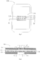
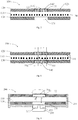
Fig. 1 is a schematic view of a display screen provided in an embodiment of the present disclosure. -
Fig. 2 is a top view of a display screen provided in an embodiment of the present disclosure. -
Fig. 3 is a sectional view ofFig 2 taken along the line AA'. -
Fig. 4 is a schematic view of a display screen provided in an embodiment of the present disclosure. -
Fig. 5 is a top view of a display screen provided in an embodiment of the present disclosure. -
Fig. 6 is a sectional view ofFig 5 taken along the line BB'. -
Fig. 7 is a schematic view of a display screen provided in an embodiment of the present disclosure. -
Fig. 8 is a schematic view of a display screen provided in an embodiment of the present disclosure. -
Fig. 9 is a schematic view of a display device provided in an embodiment of the present disclosure. -
Fig. 10 is a schematic view of a mobile terminal provided in an embodiment of the present disclosure. - The technical solutions of the embodiments of the present disclosure are clearly and completely described below with reference to the accompanying drawings in the embodiments of the present disclosure.
- Referring to
Fig. 1, Fig. 1 illustrates adisplay screen 100 provided in embodiments of the present disclosure. Thedisplay screen 100 includes a display layer and a firstlight shielding layer 120. Thedisplay layer 110 is a portion of thedisplay screen 100 and is configured to display images. Thedisplay layer 110 is provided with adisplay surface 111 towards a user, and the firstlight shielding layer 120 is arranged on thedisplay surface 111. The firstlight shielding layer 120 has afingerprint recognition area 121, thefingerprint recognition area 121 includes at least one first throughhole 122, and sensing signals emitted and received by a fingerprint unit located below the display screen pass through the first throughhole 122. - In the present embodiment, the
display screen 100 can be an organic light-emitting diode (OLED), a liquid crystal display (LCD) and the like. The firstlight shielding layer 120 can be a light-filtering layer, a polarizing layer, a color microelectronic printed layer, a flat layer and etc. The fingerprint unit can be an optical fingerprint unit, a capacitive fingerprint unit, a radio frequency fingerprint unit, an ultrasonic fingerprint unit and etc. The sensing signal can be an optical signal, an electrical signal, an ultrasonic signal and etc. - Referring to
Figs. 2 and3 , thedisplay screen 100 further includes a secondlight shielding layer 130, and the secondlight shielding layer 130 is disposed to a side of thedisplay layer 110 away from the firstlight shielding layer 120 so as to prevent structures (such as electronic circuits) below thedisplay screen 100 from being seen. The secondlight shielding layer 130 can be a light-shielding foam layer, a lightproof ink layer, or a reflective layer configured to reflect light. The secondlight shielding layer 130 can hide structures (such as the electronic circuits) below thedisplay screen 100 from view, so that thedisplay layer 110 is allowed to present a color of the secondlight shielding layer 130 when thedisplay screen 100 is in a nonluminous state. The secondlight shielding layer 130 can be black, white, or in other colors. - Referring to
Fig. 3 , in an embodiment, the fingerprint unit is the optical fingerprint unit, and the optical fingerprint unit is disposed at a side of thedisplay screen 100 away from the user. The secondlight shielding layer 130 is provided with a second throughhole 131, and the second throughhole 131 is configured so that the light signals emitted and received by the optical fingerprint unit can be transmitted through the second throughhole 131. - Further, the first through
hole 122 and the second throughhole 131 are disposed to be right opposite to each other, and the first throughhole 122 and the second throughhole 131 have a same size. In the present embodiment, the first throughhole 122 and the second throughhole 131 are allowed to form a light-transparent passage along a thickness direction of thedisplay screen 100, and the passage is disposed between the optical fingerprint unit and thefingerprint recognition area 121 so as to facilitate transmission of the light signals emitted and received by the optical fingerprint unit, reduce obstruction of thedisplay screen 100 to the signals, hence improve fingerprint recognition and acquisition efficiency. - In an embodiment, referring to
Fig. 4 , the first throughhole 122 is filled with a light-transparent layer 140. The light-transparent layer 140 is provided with afirst surface 141 away from thedisplay layer 110, the firstlight shielding layer 120 is provided with asecond surface 123 away from thedisplay layer 110, and thefirst surface 141 is flush with thesecond surface 123. In the present embodiment, by filling the light-transparent layer 140 in the first throughhole 122 and making respective surfaces, towards the user, of the light-transparent layer 140 and the firstlight shielding layer 120 flush, not only the light-transparent layer 140 does not influence light transmittance of the first throughhole 122, but also it is possible to avoid causing a uneven surface of the firstlight shielding layer 120 when the firstlight shielding layer 120 is provided with the first throughhole 122 and hence avoid influencing flatness when other functional layers are superposed on the firstlight shielding layer 120 subsequently. Preferably, a shape and size of the light-transparent layer 140 can be same with those of the first throughhole 122, which enables gapless filling between the light-transparent layer 140 and the first throughhole 122, thus making the surface of the firstlight shielding layer 120 highly flat. - In an embodiment, referring to
Fig. 5 , thefingerprint recognition area 121 is provided with a plurality of first throughholes 122 andlight shielding portions 124 among the plurality of first throughholes 122. - Referring to
Fig. 6 , thedisplay layer 110 includes a light-reflectinglayer 150, the light-reflectinglayer 150 can produce reflected light illuminated by an outside light source, and in this way, the user's eyes can not only receive the light emitted by thedisplay layer 110, but also receive the reflected light produced by the light-reflectinglayer 150. Particularly, the light-reflectinglayer 150 produces stronger reflected light when illuminated by a strong light source outside, the stronger reflected light interrupts the display image of thedisplay layer 110, influencing the user experience. The light-reflectinglayer 150 can be a reflecting sheet displaying the light source or a metal signal line in thedisplay layer 110. - Referring to
Fig. 6 , an orthographic projection area of thefingerprint recognition area 121 on the secondlight shielding layer 130 coincides with an area of the second throughhole 131. An orthographic projection area of thelight shielding portions 124 on thedisplay layer 110 coincides with a part of an area of the light-reflectinglayer 150. In the present embodiment, by making thelight shielding portions 124 in thefingerprint recognition area 121 cover the area of the light-reflectinglayer 150, the reflected light produced the area of the light-reflectinglayer 150 is blocked, and influence on the user's visual sense by the light-reflectinglayer 150 reflecting the outside light source is reduced. - In the present embodiment, the first
light shielding layer 120 is the polarizing layer and configured to prevent a reflected light signal of the light-reflectinglayer 150 from being transmitted. In other embodiments, the firstlight shielding layer 120 can also be other light-shielding components, such as the microelectronics printed layer or the flat layer. It could be understood that the firstlight shielding layer 120 can also be disposed in other positions at a side, towards the user, of the light-reflectinglayer 150. For example, the firstlight shielding layer 120 can also be disposed in thedisplay layer 110. - Referring to
Fig. 7 , the plurality of the first throughholes 122 can be filled with a light-transparent layer 140', the light-transparent layer 140' is provided with a first surface 141' away from thedisplay layer 110, the firstlight shielding layer 120 is provided with asecond surface 123 away from thedisplay layer 110, and the first surface 141' is flush with thesecond surface 123. In the present embodiment, by filling the light-transparent layer 140' in the first throughhole 122 and making respective surfaces, towards the user, of the light-transparent layer 140' and the firstlight shielding layer 120 flush, not only the light-transparent layer 140' does not influence the light transmittance of the first throughhole 122, but also it is possible to avoid causing the uneven surface of the firstlight shielding layer 120 when the firstlight shielding layer 120 is provided with the first throughhole 122 and hence avoid influencing the flatness when other functional layers are superposed on the firstlight shielding layer 120 subsequently. Preferably, a shape and size of the light-transparent layer 140' can be same with those of the first throughhole 122, which enables gapless filling between the light-transparent layer 140' and the first throughhole 122, thus making the surface of the firstlight shielding layer 120 highly flat. - Referring to
Fig. 8 , the second throughhole 131 is provided with a light-shieldingsheet 160. The light-shieldingsheet 160 is provided with a light-transparent passage 162. Specifically, the light-shieldingsheet 160 includes a light-shieldingpigment 161 and a light-transparent material, a plurality of light-transparent passages 162 is formed of the light-transparent material, the light-transparent passage 162 is along the thickness direction of thedisplay screen 100, and a light signal c emitted and received by the optical fingerprint unit is transmitted through the plurality of light-transparent passages 162. The light-shieldingsheet 160 covers the second throughhole 131, allows transmitting of the light signal c so that the light signal c emitted and received by the fingerprint unit disposed below the second throughhole 131 can be transmitted, and can reflect the light so as to hide the fingerprint unit. Preferably, reflected light of the light-shieldingsheet 160 has the same color with reflected light of the secondlight shielding layer 130, so as to make the area of the second throughhole 131 have the same display color as other areas of the secondlight shielding layer 130 when thedisplay layer 110 is in a non-display state such as in a screen-off state of the mobile terminal, thereby reducing the visual influence of the second throughhole 131 on the user and enhancing the user experience. In the present embodiment, the light-shieldingpigment 161 has the same color as the secondlight shielding layer 130, and it could be understood that, the color of the light-shieldingpigment 161 sensed by naked eyes of the user is the same as that of the secondlight shielding layer 130. The color of the secondlight shielding layer 130 can be black, white, or other colors, and correspondingly, the color of the light-shieldingpigment 161 can also be black, white, or other colors. - The light-transparent material can be a transparent material such as resin particles, glass powders, or a mixture of resin particles and glass powders. These transparent materials have a certain light transmission property and allow light to pass through. When the light-shielding
sheet 160 is added with the light-transparent material, the light transmission property of the light-shieldingsheet 160 can be increased. The light-transparent material is in a granular shape. If a granule of the light-transparent material is too small, the light transmission cannot be achieved. If the granule of the light-transparent material is too large, the light-shieldingsheet 160 and the secondlight shielding layer 130 may have a color difference. Therefore, optionally, a size of the granule of the light-transparent material is 1∼20µm. Further, if a ratio of the light-transparent material to the light-shieldingsheet 160 is too low, the light transmission property of the light-shieldingsheet 160 cannot be increased effectively. If the ratio of the light-transparent material to the light-shieldingsheet 160 is too high, the color of the light-shieldingsheet 160 will be influenced. Therefore, a mass percent of the light-transparent material to the light-shieldingsheet 160 is 1 %∼20%. - Further, an orthographic projection area of the plurality of first through
holes 122 on the secondlight shielding layer 130 can coincide with the area of the plurality of light-transparent passages 162. - The
fingerprint recognition area 121 can be circular, square, oval or in an irregular shape. The irregular shape can be a shape adapted to a contact surface between the finger and thedisplay screen 100. - The present disclosure doesn't limit the shape, size and number of the first through
hole 122 and the second throughhole 131. - The present application doesn't limit the size and number of the
fingerprint recognition area 121, and thefingerprint recognition area 121 can be a local area of thedisplay layer 110 or the whole area of thedisplay layer 110. When thefingerprint recognition area 121 is the local area of thedisplay layer 110, onefingerprint recognition area 121 or a plurality offingerprint recognition areas 121 can be provided. - Referring to
Fig. 9 , the present application further provides adisplay device 200, which includes thedisplay screen 100 according to any one of the above-mentioned embodiments, and further includes anoptical fingerprint unit 210 and amiddle frame 211. Thedisplay screen 100 and theoptical fingerprint unit 210 are fastened to themiddle frame 211. Theoptical fingerprint unit 210 is disposed at a side of thedisplay layer 110 away from the firstlight shielding layer 120 and located at a position corresponding to an opticalfingerprint recognition area 121. Theoptical fingerprint unit 210 includes alight emitter 212 and alight inductor 213, and the fingerprint recognition is performed by a first light signal emitted by thelight emitter 212 and a second light signal received by thelight inductor 213 both passing through the first throughhole 122. In other embodiment, the fingerprint unit can also be the capacitive fingerprint unit, or the radio frequency fingerprint unit, or the ultrasonic fingerprint unit. - When the finger is pressed on the
display screen 100, light emitted by thelight emitter 212 forms incident light d. The incident light d is cast on afingerprint 214 through thelight inductor 213, the second throughhole 131 and the first throughhole 122. Reflected light e is formed by the reflection of thefingerprint 214, the reflected light e is received by thelight inductor 213, and a fingerprint image of thefingerprint 214 is obtained after the reflected light e is processed. - Referring to
Fig. 10 , embodiments of the present disclosure provide amobile terminal 300, including thedisplay device 200 in any one of the above-mentioned embodiments. The mobile terminal provided in embodiments of the present disclosure can be a portable electronic device or a communication device, such as a smart phone, a personal digital assistant (PDA), a tablet computer, a notebook computer, a POS machine, or even an onboard computer, which is not limited thereto. - In the mobile terminal provided in embodiments of the present disclosure, the
fingerprint recognition area 121 of the firstlight shielding layer 120 is provided with at least one first throughhole 122, and the fingerprint unit is located at the position corresponding to thefingerprint recognition area 121. The at least one first throughhole 122 increases transmittance of the sensing signals received or emitted by thefingerprint unit 210, thereby improving the fingerprint acquisition efficiency and enhancing the user experience.
Claims (15)
- A display screen (100), comprising a display layer (110) and a first light shielding layer (120), the display layer (110) having a display surface (111) towards a user, the first light shielding layer (120) being arranged on the display surface (111), the first light shielding layer (120) having a fingerprint recognition area (121), the fingerprint recognition area (121) comprising at least one first through hole (122), the first through hole (122) being configured so that sensing signals emitted and received by a fingerprint unit (210) located below the display screen (100) can be transmitted through the first through hole (122).
- The display screen (100) according to claim 1, wherein the first light shielding layer (120) is selected from a group consisting of a light-filtering layer, a polarizing layer, a color microelectronic printed layer, and a flat layer.
- The display screen (100) according to claim 1 or 2, wherein the fingerprint unit (210) is selected from a group consisting of an optical fingerprint unit, a capacitive fingerprint unit, a radio frequency fingerprint unit, and an ultrasonic fingerprint unit.
- The display screen (100) according to one of claims 1 to 3, further comprising a second light shielding layer (130), wherein the second light shielding layer (130) is disposed at a side of the display layer (110) away from the first light shielding layer (120), the second light shielding layer (130) is provided with a second through hole (131), and the second through hole (131) and the first through hole (122) are configured so that the sensing signals emitted and received by the fingerprint unit (210) can be transmitted through the second through hole (131) and the first through hole (122).
- The display screen (100) according to claim 4, wherein the second light shielding layer (130) is selected from a group consisting of a light-shielding foam layer, a lightproof ink layer, and a reflective layer.
- The display screen (100) according to claim 4 or 5, wherein the first through hole (122) and the second through hole (131) are disposed to be right opposite to each other, and the first through hole (122) has the same size as the second through hole (131).
- The display screen (100) according to one of claims 1 to 6, wherein the first through hole (122) is filled with a light-transparent layer, the light-transparent layer is provided with a first surface away from the display layer (110), the first light shielding layer (120) is provided with a second surface away from the display layer (110), and the first surface is flush with the second surface.
- The display screen (100) according to claim 7, wherein a shape and size of the light-transparent layer are same with a shape and size of the first through hole (122).
- The display screen (100) according to claim 4, wherein the display layer (110) comprises a light-reflecting layer (150), and the first light shielding layer (120) is a polarizing layer configured to block a reflected light signal of the light-reflecting layer (150) from being emitted.
- The display screen (100) according to claim 9, wherein the fingerprint recognition area (121) is provided with a plurality of first through holes (122) and light shielding portions (124) among the plurality of first through holes (122); an orthographic projection area of the fingerprint recognition area (121) on the second light shielding layer (130) coincides with an area of the second through hole (131), and an orthographic projection area of the light shielding portion (124) on the display layer (110) coincides with an area of the light-reflecting layer (150).
- The display screen (100) according to claim 10, wherein the second through hole (131) is provided with a light-shielding sheet (160), the light-shielding sheet (160) comprises a light-shielding pigment (161) and a light-transparent material, a plurality of light-transparent passages (162) is formed of the light-transparent material, the plurality of light-transparent passages (162) is configured so that a light signal emitted and received by the optical fingerprint unit (210) can be transmitted through the plurality of light-transparent passages (162), and the light-shielding pigment (161) has the same color as the second light shielding layer (130).
- The display screen (100) according to claim 11, wherein the light-transparent material is selected from a group consisting of resin particles, glass powders, and a mixture of resin particles and glass powders.
- The display screen (100) according to claim 11, wherein an orthographic projection area of the plurality of first through holes (122) on the second light shielding layer (130) coincides with an area of the plurality of light-transparent passages (162).
- A display device, comprising a display screen (100) according to any one of claims 1 to 13, and further comprising an optical fingerprint unit (210) and a middle frame (211), the display screen (100) and the optical fingerprint unit (210) being fastened to the middle frame (211), the optical fingerprint unit (210) being disposed at a side of the display layer (110) away from the first light shielding layer (120) and located at a position corresponding to an optical fingerprint recognition area (121), the optical fingerprint unit (210) comprising a light emitter (212) and a light inductor (213), and fingerprint recognition being performed by a first light signal emitted by the light emitter (212) and a second light signal received by the light inductor (213) passing through the first through hole (122).
- A mobile terminal, comprising a display device according to claim 14.
Applications Claiming Priority (1)
| Application Number | Priority Date | Filing Date | Title |
|---|---|---|---|
| CN201710289430.3A CN107102693B (en) | 2017-04-27 | 2017-04-27 | Display screen, display device and mobile terminal |
Publications (2)
| Publication Number | Publication Date |
|---|---|
| EP3396505A1 true EP3396505A1 (en) | 2018-10-31 |
| EP3396505B1 EP3396505B1 (en) | 2020-04-22 |
Family
ID=59657283
Family Applications (1)
| Application Number | Title | Priority Date | Filing Date |
|---|---|---|---|
| EP17210894.6A Active EP3396505B1 (en) | 2017-04-27 | 2017-12-28 | Display screen, display device and mobile terminal |
Country Status (8)
| Country | Link |
|---|---|
| US (1) | US10460147B2 (en) |
| EP (1) | EP3396505B1 (en) |
| JP (1) | JP6804652B2 (en) |
| CN (2) | CN110825171B (en) |
| AU (1) | AU2018259304B2 (en) |
| ES (1) | ES2800180T3 (en) |
| TW (1) | TWI664580B (en) |
| WO (1) | WO2018196442A1 (en) |
Cited By (3)
| Publication number | Priority date | Publication date | Assignee | Title |
|---|---|---|---|---|
| CN109782482A (en) * | 2019-01-16 | 2019-05-21 | 柳州阜民科技有限公司 | Electronic equipment |
| CN114187825A (en) * | 2020-09-15 | 2022-03-15 | 北京小米移动软件有限公司 | Display assembly, method of assembling the same, and electronic device |
| EP3832362A4 (en) * | 2018-07-27 | 2022-05-04 | Boe Technology Group Co., Ltd. | DISPLAY MODULE AND DISPLAY DEVICE |
Families Citing this family (53)
| Publication number | Priority date | Publication date | Assignee | Title |
|---|---|---|---|---|
| KR101796660B1 (en) | 2016-04-19 | 2017-11-10 | 삼성전자주식회사 | Electronic device for supporting the fingerprint verification and operating method thereof |
| CN107193412B (en) | 2017-04-27 | 2020-04-14 | Oppo广东移动通信有限公司 | Display screen, display device and mobile terminal |
| CN110825171B (en) * | 2017-04-27 | 2023-06-20 | Oppo广东移动通信有限公司 | Display screen, display device and mobile terminal |
| US20190037063A1 (en) * | 2017-07-31 | 2019-01-31 | Guangdong Oppo Mobile Telecommunications Corp., Ltd. | Display panel and electronic device |
| CN107465782A (en) * | 2017-09-14 | 2017-12-12 | 深圳天珑无线科技有限公司 | Mobile terminal |
| CN107862269A (en) * | 2017-10-31 | 2018-03-30 | 苏州科阳光电科技有限公司 | Optical finger print module, optical finger print module preparation method and mobile terminal |
| KR102615589B1 (en) * | 2017-12-28 | 2023-12-18 | 엘지디스플레이 주식회사 | Fingerprint sensing display apparatus |
| CN108242462B (en) * | 2018-01-12 | 2020-08-18 | 京东方科技集团股份有限公司 | Organic light-emitting display panel, preparation method thereof, and display device |
| CN108323207B (en) * | 2018-02-06 | 2021-02-26 | 深圳市汇顶科技股份有限公司 | Under-screen biometric identification device, biometric identification component and terminal equipment |
| CN110520830A (en) * | 2018-02-26 | 2019-11-29 | 华为技术有限公司 | Mobile terminal and its display methods |
| CN108513666B (en) * | 2018-03-22 | 2022-05-17 | 深圳市汇顶科技股份有限公司 | Under-screen biological feature recognition device and electronic equipment |
| CN108681687B (en) * | 2018-03-26 | 2022-01-07 | Oppo广东移动通信有限公司 | Cover plate and manufacturing method thereof, fingerprint identification module and electronic device |
| CN108598109B (en) * | 2018-04-20 | 2021-02-09 | 上海天马有机发光显示技术有限公司 | Display panel and display device |
| CN110460691B (en) * | 2018-05-07 | 2021-10-15 | Oppo广东移动通信有限公司 | Electronic devices and display components |
| CN108829181A (en) * | 2018-05-22 | 2018-11-16 | 维沃移动通信有限公司 | Mobile terminal |
| KR102540895B1 (en) | 2018-05-30 | 2023-06-09 | 삼성디스플레이 주식회사 | Touch sensor and display device having the same |
| WO2019237353A1 (en) | 2018-06-15 | 2019-12-19 | 深圳市汇顶科技股份有限公司 | In-screen biological feature recognition apparatus and electronic device |
| CN112433561A (en) * | 2018-06-29 | 2021-03-02 | 中兴通讯股份有限公司 | Display screen module, terminal, control method of terminal and computer storage medium |
| CN109034053A (en) * | 2018-07-24 | 2018-12-18 | 京东方科技集团股份有限公司 | Display module and preparation method, control method and control device, display device |
| KR102581242B1 (en) * | 2018-08-01 | 2023-09-22 | 삼성디스플레이 주식회사 | Display device |
| CN110162203B (en) * | 2018-08-17 | 2022-11-18 | 京东方科技集团股份有限公司 | Array substrate, display panel, display device, fingerprint identification method and touch method |
| CN109270988A (en) * | 2018-08-31 | 2019-01-25 | Oppo广东移动通信有限公司 | Display components and electronic devices |
| CN109328326A (en) * | 2018-09-28 | 2019-02-12 | 深圳阜时科技有限公司 | a device |
| CN109002229B (en) * | 2018-10-15 | 2021-06-18 | 上海天马微电子有限公司 | Touch panel, display module and touch display device |
| CN109583381B (en) * | 2018-11-30 | 2020-11-10 | 京东方科技集团股份有限公司 | A texture recognition device and a self-luminous display panel |
| CN111290522B (en) * | 2018-12-10 | 2022-02-08 | 北京小米移动软件有限公司 | Fingerprint module under screen, display driving chip and mobile terminal |
| CN109561183A (en) * | 2019-01-03 | 2019-04-02 | 京东方科技集团股份有限公司 | Display screen module and mobile terminal |
| CN109784264B (en) * | 2019-01-09 | 2021-07-09 | 广州国显科技有限公司 | Optical fingerprint imaging device and display |
| CN109709712A (en) * | 2019-01-16 | 2019-05-03 | 柳州阜民科技有限公司 | A kind of backlight module, display device and electronic equipment |
| CN109887964B (en) * | 2019-02-15 | 2021-11-05 | 京东方科技集团股份有限公司 | A display device and method of making the same |
| CN109858465A (en) * | 2019-02-27 | 2019-06-07 | 昆山国显光电有限公司 | Display device for fingerprint recognition |
| CN109712527B (en) * | 2019-03-06 | 2022-11-15 | 广州国显科技有限公司 | Display device for identifying fingerprints under screen |
| CN109948512B (en) * | 2019-03-15 | 2021-06-08 | 广州国显科技有限公司 | Fingerprint identification device and display device |
| CN111726481A (en) * | 2019-03-19 | 2020-09-29 | 北京小米移动软件有限公司 | Electronic equipment |
| CN209765526U (en) * | 2019-04-10 | 2019-12-10 | 深圳市汇顶科技股份有限公司 | Optical fingerprint device and electronic equipment |
| CN113782573B (en) * | 2019-04-11 | 2024-04-05 | Oppo广东移动通信有限公司 | Display components and electronic devices |
| WO2020220304A1 (en) * | 2019-04-30 | 2020-11-05 | 深圳市汇顶科技股份有限公司 | Device for fingerprint recognition and electronic device |
| KR102795013B1 (en) | 2019-05-09 | 2025-04-15 | 삼성전자주식회사 | Display module including sensor and elecronic device including the didsplay module |
| KR102782192B1 (en) * | 2019-05-09 | 2025-03-17 | 삼성전자주식회사 | An electronic device including a display module including a sensor and a method of manufacturing the display module |
| CN113383343A (en) * | 2019-07-05 | 2021-09-10 | 深圳市柔宇科技股份有限公司 | Electronic device and flexible display device thereof |
| CN112771837B (en) * | 2019-09-03 | 2023-09-15 | Lg电子株式会社 | mobile terminal |
| WO2021087695A1 (en) * | 2019-11-04 | 2021-05-14 | 深圳市汇顶科技股份有限公司 | Optical fingerprint apparatus and electronic device |
| EP4014158B1 (en) | 2019-11-25 | 2024-09-18 | Samsung Electronics Co., Ltd. | Electronic device including fingerprint sensor |
| JP7564127B2 (en) * | 2020-04-27 | 2024-10-08 | 京東方科技集團股▲ふん▼有限公司 | Texture recognition device and opposing substrate |
| CN111524451B (en) | 2020-04-30 | 2022-03-22 | 昆山国显光电有限公司 | Display panel and display device |
| CN113743158A (en) * | 2020-05-28 | 2021-12-03 | Oppo广东移动通信有限公司 | Under-screen identification assembly and electronic equipment |
| CN111697043B (en) * | 2020-06-22 | 2023-09-22 | 合肥维信诺科技有限公司 | Display panel and preparation method thereof |
| CN111754875B (en) * | 2020-06-28 | 2022-04-19 | 合肥维信诺科技有限公司 | Display module and display device |
| KR102836622B1 (en) * | 2020-09-03 | 2025-07-21 | 삼성디스플레이 주식회사 | Display device |
| CN114255482A (en) | 2020-09-11 | 2022-03-29 | 京东方科技集团股份有限公司 | Line identification pixel circuit, line detection circuit, display substrate and display device |
| CN112420787B (en) * | 2020-11-09 | 2023-12-15 | 武汉华星光电半导体显示技术有限公司 | Display panel, display panel manufacturing method and display device |
| KR102837613B1 (en) * | 2021-07-27 | 2025-07-24 | 삼성디스플레이 주식회사 | Display device and method of manufacturing the same |
| CN114415411B (en) * | 2022-01-28 | 2024-03-26 | 武汉华星光电技术有限公司 | Under-screen monitoring display device |
Citations (5)
| Publication number | Priority date | Publication date | Assignee | Title |
|---|---|---|---|---|
| WO2001069520A2 (en) * | 2000-03-10 | 2001-09-20 | Ethentica, Inc. | Biometric sensor |
| US6327376B1 (en) * | 1997-12-04 | 2001-12-04 | U.S. Philips Corporation | Electronic apparatus comprising fingerprint sensing devices |
| US20100067757A1 (en) * | 2008-09-16 | 2010-03-18 | Shinichi Arai | Image acquisition apparatus and biometric information acquisition apparatus |
| US20110267298A1 (en) * | 2009-10-30 | 2011-11-03 | Validity Sensors, Inc. | Fingerprint sensor and integratable electronic display |
| US20150036065A1 (en) * | 2013-08-05 | 2015-02-05 | Apple Inc. | Fingerprint Sensor in an Electronic Device |
Family Cites Families (40)
| Publication number | Priority date | Publication date | Assignee | Title |
|---|---|---|---|---|
| WO2000016952A1 (en) | 1998-09-17 | 2000-03-30 | Lenert Eugene | Saw horse with self-clamping means for a workpiece being sawn and a device for securing a chain saw |
| KR100873497B1 (en) * | 2002-10-17 | 2008-12-15 | 삼성전자주식회사 | Integrated LCD with Fingerprint Recognition Device and Manufacturing Method Thereof |
| FR2857482B1 (en) * | 2003-07-09 | 2005-10-21 | Groupe Ecoles Telecomm | OPTICAL IMAGING DEVICE, IN PARTICULAR FOR THE RECOGNITION OF DIGITAL IMPRESSIONS |
| US8094129B2 (en) * | 2006-11-27 | 2012-01-10 | Microsoft Corporation | Touch sensing using shadow and reflective modes |
| JP2008205317A (en) * | 2007-02-21 | 2008-09-04 | Nec Electronics Corp | Solid-state imaging device, manufacturing method thereof, and electronic apparatus using the same |
| US20080282540A1 (en) * | 2007-05-14 | 2008-11-20 | Innovatier, Inc. | Method for making advanced smart cards with integrated electronics using isotropic thermoset adhesive materials with high quality exterior surfaces |
| US8030843B2 (en) * | 2008-07-14 | 2011-10-04 | Wisys Technology Foundation | Quantum dot phosphors for solid-state lighting devices |
| JP4962540B2 (en) * | 2009-07-30 | 2012-06-27 | 株式会社デンソー | Vehicle presence notification device |
| US9013613B2 (en) * | 2010-09-21 | 2015-04-21 | Sony Corporation | Sensor-equipped display apparatus and electronic apparatus |
| US8467177B2 (en) * | 2010-10-29 | 2013-06-18 | Apple Inc. | Displays with polarizer windows and opaque masking layers for electronic devices |
| US9030440B2 (en) * | 2012-05-18 | 2015-05-12 | Apple Inc. | Capacitive sensor packaging |
| CN103915444B (en) * | 2013-04-10 | 2016-10-19 | 上海天马微电子有限公司 | Array substrate, preparation method thereof and liquid crystal display panel |
| CN103942537A (en) * | 2014-04-04 | 2014-07-23 | 王曙光 | Liquid crystal terminal device, fingerprint image collection method and fingerprint collector |
| CN104182727B (en) * | 2014-05-16 | 2021-07-30 | 深圳印象认知技术有限公司 | Ultra-thin fingerprint and palm print acquisition device and fingerprint and palm print image acquisition method |
| CN104318205A (en) * | 2014-09-29 | 2015-01-28 | 上海箩箕技术有限公司 | Information detection display device, detection method and display method of information detection display device |
| US9829614B2 (en) * | 2015-02-02 | 2017-11-28 | Synaptics Incorporated | Optical sensor using collimator |
| CN106292844A (en) * | 2015-05-15 | 2017-01-04 | 成都艾德沃传感技术有限公司 | A kind of electronic equipment and the preparation method of electronic equipment |
| US10229358B2 (en) * | 2015-08-07 | 2019-03-12 | International Business Machines Corporation | Optimizer problem determination |
| KR102374479B1 (en) * | 2015-08-13 | 2022-03-16 | 삼성전자주식회사 | Electronic device having display and sensor |
| CN105205469A (en) * | 2015-09-25 | 2015-12-30 | 业成光电(深圳)有限公司 | Fingerprint recognition device and manufacturing method thereof |
| KR101685989B1 (en) * | 2016-01-04 | 2016-12-13 | 엘지전자 주식회사 | Mobile terminal |
| CN106098735B (en) | 2016-06-20 | 2020-10-09 | 武汉华星光电技术有限公司 | OLED display screen |
| CN106298859B (en) * | 2016-09-30 | 2018-09-04 | 京东方科技集团股份有限公司 | Touch panel and display device |
| CN106503635B (en) * | 2016-10-11 | 2019-06-28 | Oppo广东移动通信有限公司 | Cover plate for optical fingerprint identification, input assembly and electronic device |
| CN106584996B (en) * | 2016-12-06 | 2019-02-12 | Oppo广东移动通信有限公司 | Cover plate and mobile terminal |
| CN106529516A (en) * | 2016-12-29 | 2017-03-22 | 深圳天珑无线科技有限公司 | Fingerprint module group and electronic equipment |
| CN106773219B (en) * | 2017-02-07 | 2019-11-05 | 京东方科技集团股份有限公司 | a display device |
| CN106886767B (en) * | 2017-02-23 | 2019-07-05 | 京东方科技集团股份有限公司 | A kind of optical fingerprint identification device and display panel |
| US10656764B2 (en) * | 2017-02-23 | 2020-05-19 | Boe Technology Group Co., Ltd. | Touch device and display device |
| CN106847872B (en) * | 2017-03-24 | 2020-03-20 | 京东方科技集团股份有限公司 | Display device |
| CN110825171B (en) | 2017-04-27 | 2023-06-20 | Oppo广东移动通信有限公司 | Display screen, display device and mobile terminal |
| CN107193412B (en) * | 2017-04-27 | 2020-04-14 | Oppo广东移动通信有限公司 | Display screen, display device and mobile terminal |
| CN107068726B (en) * | 2017-04-27 | 2019-11-08 | 上海天马微电子有限公司 | A display panel and display device |
| CN107133613B (en) * | 2017-06-06 | 2020-06-30 | 上海天马微电子有限公司 | A display panel and display device |
| CN107065274B (en) * | 2017-06-19 | 2020-03-10 | 上海天马微电子有限公司 | Array substrate, display panel and display device |
| CN107341472B (en) * | 2017-07-04 | 2019-12-31 | 京东方科技集团股份有限公司 | An optical fingerprint identification device, its fingerprint identification method, and a display device |
| US10891460B2 (en) * | 2017-07-18 | 2021-01-12 | Will Semiconductor (Shanghai) Co. Ltd. | Systems and methods for optical sensing with angled filters |
| CN107506728B (en) * | 2017-08-23 | 2021-02-12 | 京东方科技集团股份有限公司 | Photosensitive unit, photosensitive module and photosensitive device |
| CN107657240B (en) * | 2017-10-09 | 2020-11-24 | 上海天马微电子有限公司 | Display device, fingerprint identification calibration method thereof and electronic equipment |
| CN108288681B (en) * | 2018-01-11 | 2021-01-22 | 京东方科技集团股份有限公司 | Display panel, method for manufacturing the same, and display device |
-
2017
- 2017-04-27 CN CN201911135112.7A patent/CN110825171B/en not_active Expired - Fee Related
- 2017-04-27 CN CN201710289430.3A patent/CN107102693B/en not_active Expired - Fee Related
- 2017-12-14 TW TW106143847A patent/TWI664580B/en not_active IP Right Cessation
- 2017-12-27 US US15/855,401 patent/US10460147B2/en active Active
- 2017-12-28 ES ES17210894T patent/ES2800180T3/en active Active
- 2017-12-28 EP EP17210894.6A patent/EP3396505B1/en active Active
-
2018
- 2018-01-04 AU AU2018259304A patent/AU2018259304B2/en not_active Ceased
- 2018-01-04 WO PCT/CN2018/071314 patent/WO2018196442A1/en not_active Ceased
- 2018-01-04 JP JP2019534731A patent/JP6804652B2/en not_active Expired - Fee Related
Patent Citations (5)
| Publication number | Priority date | Publication date | Assignee | Title |
|---|---|---|---|---|
| US6327376B1 (en) * | 1997-12-04 | 2001-12-04 | U.S. Philips Corporation | Electronic apparatus comprising fingerprint sensing devices |
| WO2001069520A2 (en) * | 2000-03-10 | 2001-09-20 | Ethentica, Inc. | Biometric sensor |
| US20100067757A1 (en) * | 2008-09-16 | 2010-03-18 | Shinichi Arai | Image acquisition apparatus and biometric information acquisition apparatus |
| US20110267298A1 (en) * | 2009-10-30 | 2011-11-03 | Validity Sensors, Inc. | Fingerprint sensor and integratable electronic display |
| US20150036065A1 (en) * | 2013-08-05 | 2015-02-05 | Apple Inc. | Fingerprint Sensor in an Electronic Device |
Cited By (4)
| Publication number | Priority date | Publication date | Assignee | Title |
|---|---|---|---|---|
| EP3832362A4 (en) * | 2018-07-27 | 2022-05-04 | Boe Technology Group Co., Ltd. | DISPLAY MODULE AND DISPLAY DEVICE |
| CN109782482A (en) * | 2019-01-16 | 2019-05-21 | 柳州阜民科技有限公司 | Electronic equipment |
| CN114187825A (en) * | 2020-09-15 | 2022-03-15 | 北京小米移动软件有限公司 | Display assembly, method of assembling the same, and electronic device |
| CN114187825B (en) * | 2020-09-15 | 2024-02-23 | 北京小米移动软件有限公司 | Display screen assembly, assembly method thereof and electronic equipment |
Also Published As
| Publication number | Publication date |
|---|---|
| EP3396505B1 (en) | 2020-04-22 |
| ES2800180T3 (en) | 2020-12-28 |
| CN107102693A (en) | 2017-08-29 |
| CN107102693B (en) | 2019-12-13 |
| WO2018196442A1 (en) | 2018-11-01 |
| JP2020507105A (en) | 2020-03-05 |
| JP6804652B2 (en) | 2020-12-23 |
| TW201839657A (en) | 2018-11-01 |
| CN110825171A (en) | 2020-02-21 |
| AU2018259304B2 (en) | 2020-05-21 |
| US10460147B2 (en) | 2019-10-29 |
| US20180314873A1 (en) | 2018-11-01 |
| AU2018259304A1 (en) | 2019-07-18 |
| TWI664580B (en) | 2019-07-01 |
| CN110825171B (en) | 2023-06-20 |
Similar Documents
| Publication | Publication Date | Title |
|---|---|---|
| US10460147B2 (en) | Display screen, display device and mobile terminal | |
| US10615239B2 (en) | Integration of display screen and optical fingerprint sensor | |
| CN110286514B (en) | Display panel and display device | |
| EP3396442A1 (en) | Display screen, display device and mobile terminal | |
| TWI491959B (en) | Electronic device and the method for hiding object from viewing | |
| CN107979663B (en) | Sensor components, display components and electronic equipment | |
| CN107992163B (en) | Display screen, display screen assembly and electronic equipment | |
| US20220037622A1 (en) | Display panel and display apparatus | |
| US20190286193A1 (en) | Display device | |
| US10151948B2 (en) | Display apparatus | |
| CN107948354B (en) | Display components and electronic equipment | |
| WO2019114503A1 (en) | Display screen assembly and electronic device | |
| CN107818733B (en) | Display screen assembly and electronic equipment | |
| KR20200085402A (en) | Display device including window member and manufacturing method thereof | |
| TWI499838B (en) | Display device | |
| EP3709076A1 (en) | Backlight module and display device | |
| KR20210086297A (en) | Electronic apparatus | |
| CN111862793B (en) | Display device | |
| KR102477040B1 (en) | Display apparatus and electronic apparatus | |
| HK1237914A (en) | Display screen, display device and mobile terminal | |
| JP6374242B2 (en) | Liquid crystal display device and electronic device | |
| HK1237914A1 (en) | Display screen, display device and mobile terminal | |
| JP2011227424A (en) | Liquid crystal display | |
| HK1237914B (en) | Display screen, display device and mobile terminal | |
| JP2006221022A (en) | Electrooptical apparatus and manufacturing method of electrooptical apparatus |
Legal Events
| Date | Code | Title | Description |
|---|---|---|---|
| PUAI | Public reference made under article 153(3) epc to a published international application that has entered the european phase |
Free format text: ORIGINAL CODE: 0009012 |
|
| STAA | Information on the status of an ep patent application or granted ep patent |
Free format text: STATUS: THE APPLICATION HAS BEEN PUBLISHED |
|
| AK | Designated contracting states |
Kind code of ref document: A1 Designated state(s): AL AT BE BG CH CY CZ DE DK EE ES FI FR GB GR HR HU IE IS IT LI LT LU LV MC MK MT NL NO PL PT RO RS SE SI SK SM TR |
|
| AX | Request for extension of the european patent |
Extension state: BA ME |
|
| STAA | Information on the status of an ep patent application or granted ep patent |
Free format text: STATUS: REQUEST FOR EXAMINATION WAS MADE |
|
| 17P | Request for examination filed |
Effective date: 20181122 |
|
| RBV | Designated contracting states (corrected) |
Designated state(s): AL AT BE BG CH CY CZ DE DK EE ES FI FR GB GR HR HU IE IS IT LI LT LU LV MC MK MT NL NO PL PT RO RS SE SI SK SM TR |
|
| STAA | Information on the status of an ep patent application or granted ep patent |
Free format text: STATUS: EXAMINATION IS IN PROGRESS |
|
| 17Q | First examination report despatched |
Effective date: 20190218 |
|
| RAP1 | Party data changed (applicant data changed or rights of an application transferred) |
Owner name: GUANGDONG OPPO MOBILE TELECOMMUNICATIONS CORP., LT |
|
| GRAP | Despatch of communication of intention to grant a patent |
Free format text: ORIGINAL CODE: EPIDOSNIGR1 |
|
| STAA | Information on the status of an ep patent application or granted ep patent |
Free format text: STATUS: GRANT OF PATENT IS INTENDED |
|
| INTG | Intention to grant announced |
Effective date: 20200123 |
|
| GRAS | Grant fee paid |
Free format text: ORIGINAL CODE: EPIDOSNIGR3 |
|
| GRAA | (expected) grant |
Free format text: ORIGINAL CODE: 0009210 |
|
| STAA | Information on the status of an ep patent application or granted ep patent |
Free format text: STATUS: THE PATENT HAS BEEN GRANTED |
|
| AK | Designated contracting states |
Kind code of ref document: B1 Designated state(s): AL AT BE BG CH CY CZ DE DK EE ES FI FR GB GR HR HU IE IS IT LI LT LU LV MC MK MT NL NO PL PT RO RS SE SI SK SM TR |
|
| REG | Reference to a national code |
Ref country code: CH Ref legal event code: EP |
|
| REG | Reference to a national code |
Ref country code: IE Ref legal event code: FG4D |
|
| REG | Reference to a national code |
Ref country code: DE Ref legal event code: R096 Ref document number: 602017015149 Country of ref document: DE |
|
| REG | Reference to a national code |
Ref country code: AT Ref legal event code: REF Ref document number: 1260986 Country of ref document: AT Kind code of ref document: T Effective date: 20200515 |
|
| REG | Reference to a national code |
Ref country code: NL Ref legal event code: FP |
|
| REG | Reference to a national code |
Ref country code: LT Ref legal event code: MG4D |
|
| PG25 | Lapsed in a contracting state [announced via postgrant information from national office to epo] |
Ref country code: PT Free format text: LAPSE BECAUSE OF FAILURE TO SUBMIT A TRANSLATION OF THE DESCRIPTION OR TO PAY THE FEE WITHIN THE PRESCRIBED TIME-LIMIT Effective date: 20200824 Ref country code: LT Free format text: LAPSE BECAUSE OF FAILURE TO SUBMIT A TRANSLATION OF THE DESCRIPTION OR TO PAY THE FEE WITHIN THE PRESCRIBED TIME-LIMIT Effective date: 20200422 Ref country code: IS Free format text: LAPSE BECAUSE OF FAILURE TO SUBMIT A TRANSLATION OF THE DESCRIPTION OR TO PAY THE FEE WITHIN THE PRESCRIBED TIME-LIMIT Effective date: 20200822 Ref country code: SE Free format text: LAPSE BECAUSE OF FAILURE TO SUBMIT A TRANSLATION OF THE DESCRIPTION OR TO PAY THE FEE WITHIN THE PRESCRIBED TIME-LIMIT Effective date: 20200422 Ref country code: FI Free format text: LAPSE BECAUSE OF FAILURE TO SUBMIT A TRANSLATION OF THE DESCRIPTION OR TO PAY THE FEE WITHIN THE PRESCRIBED TIME-LIMIT Effective date: 20200422 Ref country code: GR Free format text: LAPSE BECAUSE OF FAILURE TO SUBMIT A TRANSLATION OF THE DESCRIPTION OR TO PAY THE FEE WITHIN THE PRESCRIBED TIME-LIMIT Effective date: 20200723 Ref country code: NO Free format text: LAPSE BECAUSE OF FAILURE TO SUBMIT A TRANSLATION OF THE DESCRIPTION OR TO PAY THE FEE WITHIN THE PRESCRIBED TIME-LIMIT Effective date: 20200722 |
|
| REG | Reference to a national code |
Ref country code: AT Ref legal event code: MK05 Ref document number: 1260986 Country of ref document: AT Kind code of ref document: T Effective date: 20200422 |
|
| PG25 | Lapsed in a contracting state [announced via postgrant information from national office to epo] |
Ref country code: HR Free format text: LAPSE BECAUSE OF FAILURE TO SUBMIT A TRANSLATION OF THE DESCRIPTION OR TO PAY THE FEE WITHIN THE PRESCRIBED TIME-LIMIT Effective date: 20200422 Ref country code: RS Free format text: LAPSE BECAUSE OF FAILURE TO SUBMIT A TRANSLATION OF THE DESCRIPTION OR TO PAY THE FEE WITHIN THE PRESCRIBED TIME-LIMIT Effective date: 20200422 Ref country code: LV Free format text: LAPSE BECAUSE OF FAILURE TO SUBMIT A TRANSLATION OF THE DESCRIPTION OR TO PAY THE FEE WITHIN THE PRESCRIBED TIME-LIMIT Effective date: 20200422 Ref country code: BG Free format text: LAPSE BECAUSE OF FAILURE TO SUBMIT A TRANSLATION OF THE DESCRIPTION OR TO PAY THE FEE WITHIN THE PRESCRIBED TIME-LIMIT Effective date: 20200722 |
|
| PG25 | Lapsed in a contracting state [announced via postgrant information from national office to epo] |
Ref country code: AL Free format text: LAPSE BECAUSE OF FAILURE TO SUBMIT A TRANSLATION OF THE DESCRIPTION OR TO PAY THE FEE WITHIN THE PRESCRIBED TIME-LIMIT Effective date: 20200422 |
|
| REG | Reference to a national code |
Ref country code: DE Ref legal event code: R097 Ref document number: 602017015149 Country of ref document: DE |
|
| PG25 | Lapsed in a contracting state [announced via postgrant information from national office to epo] |
Ref country code: RO Free format text: LAPSE BECAUSE OF FAILURE TO SUBMIT A TRANSLATION OF THE DESCRIPTION OR TO PAY THE FEE WITHIN THE PRESCRIBED TIME-LIMIT Effective date: 20200422 Ref country code: CZ Free format text: LAPSE BECAUSE OF FAILURE TO SUBMIT A TRANSLATION OF THE DESCRIPTION OR TO PAY THE FEE WITHIN THE PRESCRIBED TIME-LIMIT Effective date: 20200422 Ref country code: AT Free format text: LAPSE BECAUSE OF FAILURE TO SUBMIT A TRANSLATION OF THE DESCRIPTION OR TO PAY THE FEE WITHIN THE PRESCRIBED TIME-LIMIT Effective date: 20200422 Ref country code: EE Free format text: LAPSE BECAUSE OF FAILURE TO SUBMIT A TRANSLATION OF THE DESCRIPTION OR TO PAY THE FEE WITHIN THE PRESCRIBED TIME-LIMIT Effective date: 20200422 Ref country code: SM Free format text: LAPSE BECAUSE OF FAILURE TO SUBMIT A TRANSLATION OF THE DESCRIPTION OR TO PAY THE FEE WITHIN THE PRESCRIBED TIME-LIMIT Effective date: 20200422 Ref country code: DK Free format text: LAPSE BECAUSE OF FAILURE TO SUBMIT A TRANSLATION OF THE DESCRIPTION OR TO PAY THE FEE WITHIN THE PRESCRIBED TIME-LIMIT Effective date: 20200422 |
|
| PG25 | Lapsed in a contracting state [announced via postgrant information from national office to epo] |
Ref country code: SK Free format text: LAPSE BECAUSE OF FAILURE TO SUBMIT A TRANSLATION OF THE DESCRIPTION OR TO PAY THE FEE WITHIN THE PRESCRIBED TIME-LIMIT Effective date: 20200422 Ref country code: PL Free format text: LAPSE BECAUSE OF FAILURE TO SUBMIT A TRANSLATION OF THE DESCRIPTION OR TO PAY THE FEE WITHIN THE PRESCRIBED TIME-LIMIT Effective date: 20200422 |
|
| PLBE | No opposition filed within time limit |
Free format text: ORIGINAL CODE: 0009261 |
|
| STAA | Information on the status of an ep patent application or granted ep patent |
Free format text: STATUS: NO OPPOSITION FILED WITHIN TIME LIMIT |
|
| 26N | No opposition filed |
Effective date: 20210125 |
|
| PG25 | Lapsed in a contracting state [announced via postgrant information from national office to epo] |
Ref country code: SI Free format text: LAPSE BECAUSE OF FAILURE TO SUBMIT A TRANSLATION OF THE DESCRIPTION OR TO PAY THE FEE WITHIN THE PRESCRIBED TIME-LIMIT Effective date: 20200422 |
|
| REG | Reference to a national code |
Ref country code: CH Ref legal event code: PL |
|
| PG25 | Lapsed in a contracting state [announced via postgrant information from national office to epo] |
Ref country code: MC Free format text: LAPSE BECAUSE OF FAILURE TO SUBMIT A TRANSLATION OF THE DESCRIPTION OR TO PAY THE FEE WITHIN THE PRESCRIBED TIME-LIMIT Effective date: 20200422 |
|
| REG | Reference to a national code |
Ref country code: BE Ref legal event code: MM Effective date: 20201231 |
|
| PG25 | Lapsed in a contracting state [announced via postgrant information from national office to epo] |
Ref country code: IE Free format text: LAPSE BECAUSE OF NON-PAYMENT OF DUE FEES Effective date: 20201228 Ref country code: LU Free format text: LAPSE BECAUSE OF NON-PAYMENT OF DUE FEES Effective date: 20201228 |
|
| PG25 | Lapsed in a contracting state [announced via postgrant information from national office to epo] |
Ref country code: LI Free format text: LAPSE BECAUSE OF NON-PAYMENT OF DUE FEES Effective date: 20201231 Ref country code: CH Free format text: LAPSE BECAUSE OF NON-PAYMENT OF DUE FEES Effective date: 20201231 |
|
| PG25 | Lapsed in a contracting state [announced via postgrant information from national office to epo] |
Ref country code: TR Free format text: LAPSE BECAUSE OF FAILURE TO SUBMIT A TRANSLATION OF THE DESCRIPTION OR TO PAY THE FEE WITHIN THE PRESCRIBED TIME-LIMIT Effective date: 20200422 Ref country code: MT Free format text: LAPSE BECAUSE OF FAILURE TO SUBMIT A TRANSLATION OF THE DESCRIPTION OR TO PAY THE FEE WITHIN THE PRESCRIBED TIME-LIMIT Effective date: 20200422 Ref country code: CY Free format text: LAPSE BECAUSE OF FAILURE TO SUBMIT A TRANSLATION OF THE DESCRIPTION OR TO PAY THE FEE WITHIN THE PRESCRIBED TIME-LIMIT Effective date: 20200422 |
|
| PG25 | Lapsed in a contracting state [announced via postgrant information from national office to epo] |
Ref country code: MK Free format text: LAPSE BECAUSE OF FAILURE TO SUBMIT A TRANSLATION OF THE DESCRIPTION OR TO PAY THE FEE WITHIN THE PRESCRIBED TIME-LIMIT Effective date: 20200422 |
|
| PG25 | Lapsed in a contracting state [announced via postgrant information from national office to epo] |
Ref country code: BE Free format text: LAPSE BECAUSE OF NON-PAYMENT OF DUE FEES Effective date: 20201231 |
|
| PGFP | Annual fee paid to national office [announced via postgrant information from national office to epo] |
Ref country code: NL Payment date: 20221124 Year of fee payment: 6 Ref country code: GB Payment date: 20221219 Year of fee payment: 6 Ref country code: FR Payment date: 20221219 Year of fee payment: 6 Ref country code: DE Payment date: 20220628 Year of fee payment: 6 |
|
| PGFP | Annual fee paid to national office [announced via postgrant information from national office to epo] |
Ref country code: ES Payment date: 20230105 Year of fee payment: 6 |
|
| PGFP | Annual fee paid to national office [announced via postgrant information from national office to epo] |
Ref country code: IT Payment date: 20221213 Year of fee payment: 6 |
|
| P01 | Opt-out of the competence of the unified patent court (upc) registered |
Effective date: 20230412 |
|
| REG | Reference to a national code |
Ref country code: DE Ref legal event code: R119 Ref document number: 602017015149 Country of ref document: DE |
|
| REG | Reference to a national code |
Ref country code: NL Ref legal event code: MM Effective date: 20240101 |
|
| GBPC | Gb: european patent ceased through non-payment of renewal fee |
Effective date: 20231228 |
|
| PG25 | Lapsed in a contracting state [announced via postgrant information from national office to epo] |
Ref country code: NL Free format text: LAPSE BECAUSE OF NON-PAYMENT OF DUE FEES Effective date: 20240101 |
|
| PG25 | Lapsed in a contracting state [announced via postgrant information from national office to epo] |
Ref country code: NL Free format text: LAPSE BECAUSE OF NON-PAYMENT OF DUE FEES Effective date: 20240101 |
|
| PG25 | Lapsed in a contracting state [announced via postgrant information from national office to epo] |
Ref country code: DE Free format text: LAPSE BECAUSE OF NON-PAYMENT OF DUE FEES Effective date: 20240702 |
|
| PG25 | Lapsed in a contracting state [announced via postgrant information from national office to epo] |
Ref country code: GB Free format text: LAPSE BECAUSE OF NON-PAYMENT OF DUE FEES Effective date: 20231228 |
|
| PG25 | Lapsed in a contracting state [announced via postgrant information from national office to epo] |
Ref country code: FR Free format text: LAPSE BECAUSE OF NON-PAYMENT OF DUE FEES Effective date: 20231231 |
|
| PG25 | Lapsed in a contracting state [announced via postgrant information from national office to epo] |
Ref country code: GB Free format text: LAPSE BECAUSE OF NON-PAYMENT OF DUE FEES Effective date: 20231228 Ref country code: FR Free format text: LAPSE BECAUSE OF NON-PAYMENT OF DUE FEES Effective date: 20231231 Ref country code: DE Free format text: LAPSE BECAUSE OF NON-PAYMENT OF DUE FEES Effective date: 20240702 |
|
| REG | Reference to a national code |
Ref country code: ES Ref legal event code: FD2A Effective date: 20250131 |
|
| PG25 | Lapsed in a contracting state [announced via postgrant information from national office to epo] |
Ref country code: ES Free format text: LAPSE BECAUSE OF NON-PAYMENT OF DUE FEES Effective date: 20231229 |
|
| PG25 | Lapsed in a contracting state [announced via postgrant information from national office to epo] |
Ref country code: IT Free format text: LAPSE BECAUSE OF NON-PAYMENT OF DUE FEES Effective date: 20231228 |