KR20200085402A - Display device including window member and manufacturing method thereof - Google Patents
Display device including window member and manufacturing method thereof Download PDFInfo
- Publication number
- KR20200085402A KR20200085402A KR1020190001348A KR20190001348A KR20200085402A KR 20200085402 A KR20200085402 A KR 20200085402A KR 1020190001348 A KR1020190001348 A KR 1020190001348A KR 20190001348 A KR20190001348 A KR 20190001348A KR 20200085402 A KR20200085402 A KR 20200085402A
- Authority
- KR
- South Korea
- Prior art keywords
- layer
- printing layer
- display device
- printing
- printed
- Prior art date
Links
- 238000004519 manufacturing process Methods 0.000 title claims abstract description 20
- 230000002093 peripheral effect Effects 0.000 claims abstract description 13
- 239000010410 layer Substances 0.000 claims description 249
- 238000007639 printing Methods 0.000 claims description 169
- 238000000034 method Methods 0.000 claims description 12
- 238000000576 coating method Methods 0.000 claims description 10
- 238000000059 patterning Methods 0.000 claims description 10
- 239000012790 adhesive layer Substances 0.000 claims description 7
- 238000005507 spraying Methods 0.000 claims description 7
- 239000011248 coating agent Substances 0.000 claims description 6
- 230000008021 deposition Effects 0.000 claims description 5
- 238000000151 deposition Methods 0.000 claims description 5
- 238000004140 cleaning Methods 0.000 claims description 2
- 239000000758 substrate Substances 0.000 description 10
- 238000005538 encapsulation Methods 0.000 description 9
- 239000003086 colorant Substances 0.000 description 6
- 238000005137 deposition process Methods 0.000 description 4
- 239000000463 material Substances 0.000 description 4
- 230000005540 biological transmission Effects 0.000 description 3
- 239000007921 spray Substances 0.000 description 3
- 239000004925 Acrylic resin Substances 0.000 description 2
- 229920000178 Acrylic resin Polymers 0.000 description 2
- 230000015572 biosynthetic process Effects 0.000 description 2
- 239000003822 epoxy resin Substances 0.000 description 2
- 239000011521 glass Substances 0.000 description 2
- 239000011810 insulating material Substances 0.000 description 2
- 239000004973 liquid crystal related substance Substances 0.000 description 2
- 239000000049 pigment Substances 0.000 description 2
- 239000004033 plastic Substances 0.000 description 2
- 229920003023 plastic Polymers 0.000 description 2
- 239000002985 plastic film Substances 0.000 description 2
- 229920006255 plastic film Polymers 0.000 description 2
- 229920000647 polyepoxide Polymers 0.000 description 2
- 229920001296 polysiloxane Polymers 0.000 description 2
- 229920002635 polyurethane Polymers 0.000 description 2
- 239000004814 polyurethane Substances 0.000 description 2
- 239000011347 resin Substances 0.000 description 2
- 229920005989 resin Polymers 0.000 description 2
- 239000010980 sapphire Substances 0.000 description 2
- 229910052594 sapphire Inorganic materials 0.000 description 2
- 238000007789 sealing Methods 0.000 description 2
- BQCADISMDOOEFD-UHFFFAOYSA-N Silver Chemical compound [Ag] BQCADISMDOOEFD-UHFFFAOYSA-N 0.000 description 1
- 238000013459 approach Methods 0.000 description 1
- 230000000903 blocking effect Effects 0.000 description 1
- 230000005674 electromagnetic induction Effects 0.000 description 1
- 230000005484 gravity Effects 0.000 description 1
- 239000012535 impurity Substances 0.000 description 1
- 230000001678 irradiating effect Effects 0.000 description 1
- 229910052751 metal Inorganic materials 0.000 description 1
- 239000002184 metal Substances 0.000 description 1
- 238000012986 modification Methods 0.000 description 1
- 230000004048 modification Effects 0.000 description 1
- 239000002245 particle Substances 0.000 description 1
- 238000012831 peritoneal equilibrium test Methods 0.000 description 1
- 238000012636 positron electron tomography Methods 0.000 description 1
- 238000012877 positron emission topography Methods 0.000 description 1
- 229910052709 silver Inorganic materials 0.000 description 1
- 239000004332 silver Substances 0.000 description 1
- 239000004071 soot Substances 0.000 description 1
- 238000007740 vapor deposition Methods 0.000 description 1
- 210000000707 wrist Anatomy 0.000 description 1
Images


Classifications
-
- H—ELECTRICITY
- H05—ELECTRIC TECHNIQUES NOT OTHERWISE PROVIDED FOR
- H05K—PRINTED CIRCUITS; CASINGS OR CONSTRUCTIONAL DETAILS OF ELECTRIC APPARATUS; MANUFACTURE OF ASSEMBLAGES OF ELECTRICAL COMPONENTS
- H05K5/00—Casings, cabinets or drawers for electric apparatus
- H05K5/0017—Casings, cabinets or drawers for electric apparatus with operator interface units
-
- H—ELECTRICITY
- H10—SEMICONDUCTOR DEVICES; ELECTRIC SOLID-STATE DEVICES NOT OTHERWISE PROVIDED FOR
- H10K—ORGANIC ELECTRIC SOLID-STATE DEVICES
- H10K59/00—Integrated devices, or assemblies of multiple devices, comprising at least one organic light-emitting element covered by group H10K50/00
- H10K59/10—OLED displays
- H10K59/12—Active-matrix OLED [AMOLED] displays
-
- G—PHYSICS
- G09—EDUCATION; CRYPTOGRAPHY; DISPLAY; ADVERTISING; SEALS
- G09F—DISPLAYING; ADVERTISING; SIGNS; LABELS OR NAME-PLATES; SEALS
- G09F9/00—Indicating arrangements for variable information in which the information is built-up on a support by selection or combination of individual elements
- G09F9/30—Indicating arrangements for variable information in which the information is built-up on a support by selection or combination of individual elements in which the desired character or characters are formed by combining individual elements
-
- G—PHYSICS
- G02—OPTICS
- G02B—OPTICAL ELEMENTS, SYSTEMS OR APPARATUS
- G02B1/00—Optical elements characterised by the material of which they are made; Optical coatings for optical elements
- G02B1/10—Optical coatings produced by application to, or surface treatment of, optical elements
- G02B1/14—Protective coatings, e.g. hard coatings
-
- G—PHYSICS
- G02—OPTICS
- G02F—OPTICAL DEVICES OR ARRANGEMENTS FOR THE CONTROL OF LIGHT BY MODIFICATION OF THE OPTICAL PROPERTIES OF THE MEDIA OF THE ELEMENTS INVOLVED THEREIN; NON-LINEAR OPTICS; FREQUENCY-CHANGING OF LIGHT; OPTICAL LOGIC ELEMENTS; OPTICAL ANALOGUE/DIGITAL CONVERTERS
- G02F1/00—Devices or arrangements for the control of the intensity, colour, phase, polarisation or direction of light arriving from an independent light source, e.g. switching, gating or modulating; Non-linear optics
- G02F1/01—Devices or arrangements for the control of the intensity, colour, phase, polarisation or direction of light arriving from an independent light source, e.g. switching, gating or modulating; Non-linear optics for the control of the intensity, phase, polarisation or colour
- G02F1/13—Devices or arrangements for the control of the intensity, colour, phase, polarisation or direction of light arriving from an independent light source, e.g. switching, gating or modulating; Non-linear optics for the control of the intensity, phase, polarisation or colour based on liquid crystals, e.g. single liquid crystal display cells
- G02F1/133—Constructional arrangements; Operation of liquid crystal cells; Circuit arrangements
- G02F1/1333—Constructional arrangements; Manufacturing methods
- G02F1/133308—Support structures for LCD panels, e.g. frames or bezels
- G02F1/133331—Cover glasses
-
- G—PHYSICS
- G06—COMPUTING; CALCULATING OR COUNTING
- G06F—ELECTRIC DIGITAL DATA PROCESSING
- G06F1/00—Details not covered by groups G06F3/00 - G06F13/00 and G06F21/00
- G06F1/16—Constructional details or arrangements
- G06F1/1613—Constructional details or arrangements for portable computers
- G06F1/1633—Constructional details or arrangements of portable computers not specific to the type of enclosures covered by groups G06F1/1615 - G06F1/1626
- G06F1/1637—Details related to the display arrangement, including those related to the mounting of the display in the housing
-
- H—ELECTRICITY
- H05—ELECTRIC TECHNIQUES NOT OTHERWISE PROVIDED FOR
- H05K—PRINTED CIRCUITS; CASINGS OR CONSTRUCTIONAL DETAILS OF ELECTRIC APPARATUS; MANUFACTURE OF ASSEMBLAGES OF ELECTRICAL COMPONENTS
- H05K5/00—Casings, cabinets or drawers for electric apparatus
- H05K5/02—Details
- H05K5/03—Covers
-
- H—ELECTRICITY
- H10—SEMICONDUCTOR DEVICES; ELECTRIC SOLID-STATE DEVICES NOT OTHERWISE PROVIDED FOR
- H10K—ORGANIC ELECTRIC SOLID-STATE DEVICES
- H10K59/00—Integrated devices, or assemblies of multiple devices, comprising at least one organic light-emitting element covered by group H10K50/00
- H10K59/10—OLED displays
- H10K59/12—Active-matrix OLED [AMOLED] displays
- H10K59/122—Pixel-defining structures or layers, e.g. banks
-
- H—ELECTRICITY
- H10—SEMICONDUCTOR DEVICES; ELECTRIC SOLID-STATE DEVICES NOT OTHERWISE PROVIDED FOR
- H10K—ORGANIC ELECTRIC SOLID-STATE DEVICES
- H10K71/00—Manufacture or treatment specially adapted for the organic devices covered by this subclass
-
- H—ELECTRICITY
- H10—SEMICONDUCTOR DEVICES; ELECTRIC SOLID-STATE DEVICES NOT OTHERWISE PROVIDED FOR
- H10K—ORGANIC ELECTRIC SOLID-STATE DEVICES
- H10K71/00—Manufacture or treatment specially adapted for the organic devices covered by this subclass
- H10K71/10—Deposition of organic active material
- H10K71/12—Deposition of organic active material using liquid deposition, e.g. spin coating
- H10K71/13—Deposition of organic active material using liquid deposition, e.g. spin coating using printing techniques, e.g. ink-jet printing or screen printing
-
- G02F2001/133331—
Abstract
Description
본 개시는 윈도우 부재를 포함하는 표시 장치 및 표시 장치의 제조 방법에 관한 것이다.The present disclosure relates to a display device including a window member and a method for manufacturing the display device.
액정 표시 장치(liquid crystal display, LCD), 유기 발광 표시 장치(organic light emitting diode display, OLED display) 등의 표시 장치는 영상을 표시할 수 있는 복수의 화소를 포함하는 표시 패널 및 윈도우 부재를 포함한다.2. Description of the Related Art Display devices such as liquid crystal displays (LCDs) and organic light emitting diode displays (OLEDs) include a display panel and a window member including a plurality of pixels capable of displaying an image. .
윈도우 부재는 투명하여 빛이 투과될 수 있는 영역 및 빛이 투과되지 않는 영역을 포함할 수 있다.The window member may be transparent and include an area through which light can be transmitted and an area through which light is not transmitted.
본 기재는 윈도우 부재의 인쇄층의 디자인의 다양성 및 고급감을 높이기 위한 것이다.This description is intended to increase the design diversity and luxury of the printed layer of the window member.
본 발명의 한 실시예에 따른 표시 장치는 복수의 화소를 포함하는 표시 영역 및 상기 표시 영역의 바깥쪽에 위치하는 주변 영역을 포함하는 표시 패널, 그리고 상기 표시 영역에 대응하는 투과 영역 및 상기 주변 영역에 대응하는 비투과 영역을 포함하는 윈도우 부재를 포함하고, 상기 윈도우 부재는 베이스 부재 및 상기 베이스 부재의 제1면 상에 직접 형성되어 있는 제1 인쇄층을 포함하고, 상기 제1 인쇄층은 제거부를 포함하고, 상기 제거부는 상기 비투과 영역에 위치한다.A display device according to an exemplary embodiment of the present invention includes a display area including a plurality of pixels and a display panel including a peripheral area located outside the display area, and a transmissive area and the peripheral area corresponding to the display area. A window member comprising a corresponding non-transmissive region, the window member includes a base member and a first printing layer formed directly on the first surface of the base member, and the first printing layer includes a removing portion And, the removal portion is located in the non-transmissive region.
상기 제1 인쇄층 상에 위치하는 제2 인쇄층을 더 포함하고, 상기 제2 인쇄층의 색은 상기 제1 인쇄층의 색과 다를 수 있다.Further comprising a second print layer located on the first print layer, the color of the second print layer may be different from the color of the first print layer.
상기 제1 인쇄층의 색은 흑색이고, 상기 제2 인쇄층의 색은 유채색 또는 금속색일 수 있다.The color of the first printed layer may be black, and the color of the second printed layer may be chromatic or metallic.
상기 제2 인쇄층은 상기 제거부와 중첩할 수 있다.The second printed layer may overlap the removal portion.
상기 제2 인쇄층은 상기 제1 인쇄층과 접촉하는 부분을 포함하고, 상기 제2 인쇄층은 상기 제거부 안의 공간을 채우고 있을 수 있다.The second print layer may include a portion in contact with the first print layer, and the second print layer may fill a space in the removal portion.
상기 제거부 안의 공간의 적어도 일부는 상기 제2 인쇄층으로 채워져 있지 않을 수 있다.At least a part of the space in the removal portion may not be filled with the second printing layer.
상기 제2 인쇄층과 상기 제1 인쇄층 사이에 위치하는 필름을 더 포함할 수 있다.A film positioned between the second printing layer and the first printing layer may be further included.
상기 제2 인쇄층과 상기 제1 인쇄층 사이에 위치하는 점착층을 더 포함할 수 있다.An adhesive layer positioned between the second printing layer and the first printing layer may be further included.
상기 제1면은 상기 표시 패널을 향하는 면일 수 있다.The first surface may be a surface facing the display panel.
상기 제거부는 레이저 패터닝으로 형성되어 있을 수 있다.The removal portion may be formed by laser patterning.
한 실시예에 따른 표시 장치는 복수의 화소를 포함하는 표시 영역 및 상기 표시 영역의 바깥쪽에 위치하는 주변 영역을 포함하는 표시 패널, 그리고 상기 표시 영역에 대응하는 투과 영역 및 상기 주변 영역에 대응하는 비투과 영역을 포함하는 윈도우 부재를 포함하고, 상기 윈도우 부재는, 베이스 부재 및 상기 베이스 부재의 제1면과 접촉하는 제1 인쇄층, 그리고 상기 제1 인쇄층과 다른 층에 위치하는 제2 인쇄층을 포함하고, 상기 제1 인쇄층은, 상기 제1면까지 상기 제1 인쇄층이 제거되어 있는 개구부를 포함하고, 상기 제2 인쇄층은 상기 개구부와 중첩한다.The display device according to an exemplary embodiment includes a display area including a plurality of pixels and a display panel including a peripheral area located outside the display area, a transmissive area corresponding to the display area, and a non-transmissive area corresponding to the peripheral area A window member comprising an area, the window member comprising: a first printing layer in contact with a base member and a first surface of the base member, and a second printing layer positioned on a different layer from the first printing layer. The first printing layer includes an opening in which the first printing layer is removed to the first surface, and the second printing layer overlaps the opening.
상기 제2 인쇄층의 색은 상기 제1 인쇄층의 색과 다를 수 있다.The color of the second printed layer may be different from the color of the first printed layer.
상기 제1 인쇄층의 색은 흑색이고, 상기 제2 인쇄층의 색은 유채색 또는 금속색일 수 있다.The color of the first printed layer may be black, and the color of the second printed layer may be chromatic or metallic.
상기 제2 인쇄층은 상기 제1 인쇄층과 접촉하는 부분을 포함하고, 상기 제2 인쇄층은 상기 제거부 안의 공간을 채우고 있을 수 있다.The second print layer may include a portion in contact with the first print layer, and the second print layer may fill a space in the removal portion.
상기 제거부 안의 공간의 적어도 일부는 상기 제2 인쇄층으로 채워져 있지 않을 수 있다.At least a part of the space in the removal portion may not be filled with the second printing layer.
상기 제2 인쇄층과 상기 제1 인쇄층 사이에 위치하는 필름을 더 포함할 수 있다.A film positioned between the second printing layer and the first printing layer may be further included.
상기 제2 인쇄층과 상기 제1 인쇄층 사이에 위치하는 점착층을 더 포함할 수 있다.An adhesive layer positioned between the second printing layer and the first printing layer may be further included.
상기 제1면은 상기 표시 패널을 향하는 면일 수 있다.The first surface may be a surface facing the display panel.
상기 제거부는 레이저 패터닝으로 형성되어 있을 수 있다.The removal portion may be formed by laser patterning.
한 실시예에 따른 표시 장치의 제조 방법은 베이스 부재의 비투과 영역의 제1면 상에 제1 인쇄층을 형성하는 단계, 상기 제1 인쇄층을 레이저를 이용해 패터닝하여 제거부를 형성하는 단계, 상기 제거부가 형성된 상기 제1 인쇄층 상에 제2 인쇄층을 형성하는 단계, 복수의 화소를 포함하는 표시 패널을 마련하는 단계, 그리고 상기 제1 인쇄층 및 상기 제2 인쇄층이 형성된 상기 베이스 부재와 상기 표시 패널을 합착하는 단계를 포함하고, 상기 제2 인쇄층은 상기 제거부와 중첩한다.A method of manufacturing a display device according to an embodiment includes forming a first printing layer on a first surface of a non-transmissive region of a base member, forming a removal unit by patterning the first printing layer using a laser, and removing Forming a second print layer on the first print layer on which an additional portion is formed, providing a display panel including a plurality of pixels, and the base member and the base on which the first print layer and the second print layer are formed And bonding the display panel, and the second printed layer overlaps the removal unit.
상기 제1면 상에 상기 제1 인쇄층을 형성하는 단계는, 증착, 스프레이, 코팅, 인쇄 중 하나를 이용할 수 있다.The step of forming the first printing layer on the first surface may use one of deposition, spraying, coating, and printing.
상기 제1 인쇄층 상에 상기 제2 인쇄층을 형성하는 단계는, 증착, 스프레이, 코팅, 인쇄 중 하나를 이용할 수 있다.The step of forming the second printing layer on the first printing layer may use one of deposition, spraying, coating, and printing.
상기 제1 인쇄층 상에 상기 제2 인쇄층을 형성하는 단계는 필름 위에 상기 제2 인쇄층을 형성하는 단계, 그리고 상기 필름을 상기 제1 인쇄층 상에 부착시키는 단계를 포함할 수 있다.The forming of the second printing layer on the first printing layer may include forming the second printing layer on the film, and attaching the film on the first printing layer.
상기 제1 인쇄층에 상기 제거부를 형성하는 단계와 상기 제2 인쇄층을 형성하는 단계 사이에, 상기 베이스 부재를 세정하는 단계를 더 포함할 수 있다.Between the step of forming the removal portion on the first print layer and the step of forming the second print layer, the step of cleaning the base member may be further included.
상기 제2 인쇄층의 색은 상기 제1 인쇄층의 색과 다를 수 있다.The color of the second printed layer may be different from the color of the first printed layer.
본 발명의 실시예들에 따르면, 윈도우 부재의 인쇄층의 디자인의 다양성 및 고급감을 높일 수 있다.According to embodiments of the present invention, it is possible to increase the diversity and sense of quality of the design of the printed layer of the window member.
도 1은 본 발명의 한 실시예에 따른 표시 장치의 분해 사시도이고,
도 2 및 도 3은 각각 도 1에 도시한 표시 장치의 윈도우 부재를 IIa-IIb 선을 따라 잘라 도시한 단면도이고,
도 4는 본 발명의 한 실시예에 따른 표시 장치의 윈도우 부재의 제조 방법의 순서도이고,
도 5는 본 발명의 한 실시예에 따른 표시 장치의 윈도우 부재의 제조 방법의 한 단계에서의 윈도우 부재의 평면도이고,
도 6은 도 5에 도시한 윈도우 부재를 Va-Vb 선을 따라 잘라 도시한 단면도이고,
도 7은 본 발명의 한 실시예에 따른 표시 장치의 윈도우 부재의 제조 방법의 한 단계에서의 윈도우 부재의 평면도이고,
도 8은 도 7에 도시한 윈도우 부재를 VIIa-VIIb 선을 따라 잘라 도시한 단면도이고,
도 9는 본 발명의 한 실시예에 따른 표시 장치의 윈도우 부재의 제조 방법의 한 단계에서의 윈도우 부재의 평면도이고,
도 10은 도 9에 도시한 윈도우 부재를 IXa-IXb 선을 따라 잘라 도시한 단면도이고,
도 11은 본 발명의 한 실시예에 따른 표시 장치의 윈도우 부재의 단면도이고,
도 12는 본 발명의 한 실시예에 따른 표시 장치의 윈도우 부재의 인쇄층의 패턴의 다양한 예를 도시한다.1 is an exploded perspective view of a display device according to an exemplary embodiment of the present invention,
2 and 3 are cross-sectional views of the window member of the display device illustrated in FIG. 1 taken along line IIa-IIb, respectively.
4 is a flowchart of a method for manufacturing a window member of a display device according to an exemplary embodiment of the present invention,
5 is a plan view of a window member in one step of a method of manufacturing a window member of a display device according to an exemplary embodiment of the present invention,
6 is a cross-sectional view of the window member shown in FIG. 5 taken along the line Va-Vb,
7 is a plan view of a window member in one step of a method of manufacturing a window member of a display device according to an exemplary embodiment of the present invention,
8 is a cross-sectional view of the window member shown in FIG. 7 taken along line VIIa-VIIb,
9 is a plan view of a window member in one step of a method of manufacturing a window member of a display device according to an exemplary embodiment of the present invention,
10 is a cross-sectional view of the window member shown in FIG. 9 taken along line IXa-IXb,
11 is a cross-sectional view of a window member of a display device according to an exemplary embodiment of the present invention,
12 illustrates various examples of patterns of a printed layer of a window member of a display device according to an embodiment of the present invention.
이하, 첨부한 도면을 참고로 하여 본 발명의 여러 실시예들에 대하여 본 발명이 속하는 기술 분야에서 통상의 지식을 가진 자가 용이하게 실시할 수 있도록 상세히 설명한다. 본 발명은 여러 가지 상이한 형태로 구현될 수 있으며 여기에서 설명하는 실시예들에 한정되지 않는다.Hereinafter, various embodiments of the present invention will be described in detail with reference to the accompanying drawings so that those skilled in the art to which the present invention pertains can easily practice. The present invention can be implemented in many different forms and is not limited to the embodiments described herein.
본 발명을 명확하게 설명하기 위해서 설명과 관계없는 부분은 생략하였으며, 명세서 전체를 통하여 동일 또는 유사한 구성요소에 대해서는 동일한 참조 부호를 붙이도록 한다.In order to clearly describe the present invention, parts irrelevant to the description are omitted, and the same reference numerals are assigned to the same or similar elements throughout the specification.
도면에서 나타난 각 구성의 크기 및 두께는 설명의 편의를 위해 임의로 나타내었으므로, 본 발명이 반드시 도시된 바에 한정되지 않는다. 도면에서 여러 층 및 영역을 명확하게 표현하기 위하여 두께를 확대하여 나타내었다. 그리고 도면에서, 설명의 편의를 위해, 일부 층 및 영역의 두께를 과장되게 나타내었다.Since the size and thickness of each component shown in the drawings are arbitrarily shown for convenience of description, the present invention is not necessarily limited to what is shown. In the drawings, thicknesses are enlarged to clearly represent various layers and regions. In the drawings, thicknesses of some layers and regions are exaggerated for convenience of description.
층, 막, 영역, 판 등의 부분이 다른 부분 "위에" 또는 "상에" 있다고 할 때, 이는 다른 부분 "바로 위에" 있는 경우뿐 아니라 그 중간에 또 다른 부분이 있는 경우도 포함한다. 반대로 어떤 부분이 다른 부분 "바로 위에" 있다고 할 때에는 중간에 다른 부분이 없는 것을 뜻한다. 또한, 기준이 되는 부분 "위에" 또는 "상에" 있다고 하는 것은 기준이 되는 부분의 위 또는 아래에 위치하는 것이고, 반드시 중력 반대 방향 쪽으로 "위에" 또는 "상에" 위치하는 것을 의미하는 것은 아니다.When a portion of a layer, film, region, plate, etc. is said to be "above" or "on" another portion, this includes the case where another portion is "directly over" the other portion, as well as another portion in the middle. Conversely, when one part is "just above" another part, it means that there is no other part in the middle. Also, being "above" or "on" the reference portion is positioned above or below the reference portion, and does not necessarily mean "above" or "on" the opposite direction of gravity. .
명세서 전체에서, 어떤 부분이 어떤 구성요소를 "포함" 한다고 할 때, 이는 특별히 반대되는 기재가 없는 한 다른 구성요소를 제외하는 것이 아니라 다른 구성 요소를 더 포함할 수 있는 것을 의미한다.Throughout the specification, when a part “includes” a certain component, it means that the component may further include other components, not to exclude other components, unless otherwise stated.
명세서 전체에서, 평면 뷰(in a plan view)는 서로 교차하는 두 방향(예를 들어, 제1방향(DR1) 및 제2방향(DR2))에 평행한 면을 관찰하는 뷰를 의미하고(평면상이라고도 표현함), 단면 뷰(in a cross-sectional view)는 제1방향(DR1) 및 제2방향(DR2)에 평행한 면에 수직인 방향(예를 들어, 제3방향(DR3))으로 자른 면을 관찰하는 뷰를 의미한다. 또한, 두 구성 요소가 중첩한다고 할 때는 다른 언급이 없는 한 두 구성 요소가 제3방향(DR3)으로(예를 들어, 기판의 윗면에 수직인 방향으로) 중첩하는 것을 의미한다.Throughout the specification, in a plan view means a view observing a plane parallel to two directions intersecting each other (for example, the first direction DR1 and the second direction DR2). Also referred to as an image), a cross-sectional view (in a cross-sectional view) in the direction perpendicular to the surface parallel to the first direction (DR1) and the second direction (DR2) (for example, the third direction (DR3)) It means the view observing the cut side. In addition, when two components overlap, it means that the two components overlap in the third direction DR3 (for example, in a direction perpendicular to the top surface of the substrate) unless otherwise specified.
먼저, 도 1을 참조하여 한 실시예에 따른 표시 장치에 대해 설명한다.First, a display device according to an exemplary embodiment will be described with reference to FIG. 1.
도 1은 한 실시예에 따른 표시 장치의 분해 사시도이다.1 is an exploded perspective view of a display device according to an exemplary embodiment.
도 1은 본 발명의 한 실시예에 따른 표시 장치(1000)의 예로서 휴대용 단말기를 도시하였으나 이에 한정되는 것은 아니다. 휴대용 단말기는 태블릿 PC, 스마트폰, PDA(Personal Digital Assistant), PMP(Portable Multimedia Player), 게임기, 손목 시계형 전자 기기 등 다양한 표시 장치일 수 있다. 그러나, 본 발명의 실시예에 따른 표시 장치(1000)가 이에 한정되는 것은 아니다. 본 발명은 텔레비전 또는 외부 광고판과 같은 대형 전자 장비를 비롯하여, 퍼스널 컴퓨터, 노트북 컴퓨터, 자동차 네이게이션 유닛, 카메라와 같은 중소형 전자 장비 등일 수도 있다. 이것들은 단지 실시예로서 제시된 것들로서, 본 발명의 개념에서 벗어나지 않은 이상 다른 전자 기기에도 채용될 수 있다.1 illustrates a portable terminal as an example of the
도 1에 도시된 것과 같이, 한 실시예에 따른 표시 장치(1000)는 표시 패널(100), 윈도우 부재(200), 그리고 케이스 부재(150)를 포함할 수 있다.1, the
표시 패널(100)은 영상을 표시할 수 있는 영역인 표시 영역(DA) 및 표시 영역(DA)의 바깥쪽에 위치하는 주변 영역(PA)을 포함할 수 있다. 표시 영역(DA)은 영상을 표시하는 단위인 복수의 화소(PX)를 포함할 수 있다. 주변 영역(PA)은 영상을 표시하지 않는 영역일 수 있다.The
표시 패널(100)은 액정 표시 장치, 유기 발광 표시 장치 등 다양한 표시 장치의 표시 패널일 수 있다.The
표시 패널(100)은 기판(110), 그리고 봉지층(120)을 포함할 수 있다. 기판(110)과 봉지층(120) 사이에는 복수의 신호선, 복수의 트랜지스터, 그리고 복수의 화소 전극 등이 위치할 수 있다. 화소 전극은 적어도 하나의 트랜지스터와 전기적으로 연결되어 있을 수 있다.The
예를 들어, 표시 패널(100)이 발광 표시 장치의 표시 패널인 경우, 기판(110)과 봉지층(120) 사이에는 복수의 발광 소자가 위치할 수 있다.For example, when the
발광 소자는 화소 전극, 공통 전극, 그리고 화소 전극과 공통 전극 사이에 위치하는 적어도 하나의 발광층을 포함할 수 있다. 발광층은 유기 발광 재료를 포함하는 유기 발광층 또는 무기 발광 재료를 포함하는 무기 발광층일 수 있다.The light emitting device may include a pixel electrode, a common electrode, and at least one light emitting layer positioned between the pixel electrode and the common electrode. The emission layer may be an organic emission layer including an organic emission material or an inorganic emission layer including an inorganic emission material.
각 화소(PX)에는 하나씩의 화소 전극이 위치할 수 있으나, 이에 한정되는 것은 아니다.One pixel electrode may be positioned in each pixel PX, but is not limited thereto.
봉지층(120)은 기판일 수도 있고 복수의 절연층을 포함할 수 있다. 예를 들어, 봉지층(120)은 적어도 하나의 무기 절연층과 적어도 하나의 유기 절연층을 포함할 수 있다. 봉지층(120)은 발광 소자를 외부로부터 밀봉하여 발광 소자를 보호할 수 있다.The
봉지층(120)은 기판(110)의 가장자리 영역의 일면을 덮지 않고 노출할 수 있다.The
표시 패널(100)은 영상을 표시하는 표시면과 표시면에 대향하는 배면을 가질 수 있다. 표시면은 봉지층(120)의 상면이고, 배면은 기판(110)의 하면으로 정의될 수 있다.The
영상이 표시되는 표시면은 제1방향(DR1)과 제2방향(DR2)이 정의하는 면과 대체로 평행할 수 있고, 표시면의 법선 방향은 제3방향(DR3)일 수 있다. 그러나, 이러한 방향들이 지시하는 방향은 상대적인 개념으로서 다른 방향으로 변환될 수 있다.The display surface on which the image is displayed may be substantially parallel to a surface defined by the first direction DR1 and the second direction DR2, and the normal direction of the display surface may be the third direction DR3. However, the directions indicated by these directions can be converted into other directions as a relative concept.
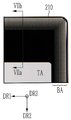
윈도우 부재(200)는 표시 패널(100)과 중첩할 수 있다. 도 1에서, 윈도우 부재(200)는 표시 패널(100)의 상부에 위치할 수 있다.The
윈도우 부재(200)는 표시 패널(100)이 제공하는 영상을 투과시킬 수 있는 투과 영역(TA)과 투과 영역(TA) 바깥쪽에 위치하는 비투과 영역(BA)을 포함할 수 있다. 투과 영역(TA)은 표시 패널(100)의 표시 영역(DA)에 대응될 수 있고 비투과 영역(BA)은 표시 패널(100)의 주변 영역(PA)에 대응될 수 있다. 비투과 영역(BA)은 윈도우 부재(200)의 가장자리 영역에 위치하고, 투과 영역(TA)은 비투과 영역(BA)으로 둘러싸여 있을 수 있다.The
케이스 부재(150)는 표시 패널(100)의 하부에 배치되어 표시 패널(100)을 수납할 수 있다. 케이스 부재(150)는 표시 패널(100)을 사이에 두고 윈도우 부재(200)와 결합할 수 있다.The
한 실시예에 따른 표시 장치(1000)는 가요성 인쇄 회로 기판(500)을 더 포함할 수 있다.The
가요성 인쇄 회로 기판(500)의 일단은 봉지층(120)에 의해 노출된 기판(110)의 일면 상에 전기적으로 연결될 수 있다. 가요성 인쇄 회로 기판(500)은 표시 패널(100)의 배면 쪽으로 벤딩되어 있을 수 있다.One end of the flexible printed
한 실시예에 따른 표시 장치(1000)는 가요성 인쇄 회로 기판(500)의 타단에 전기적으로 연결되어 있는 인쇄 회로 기판(600)을 더 포함할 수 있다.The
인쇄 회로 기판(600)은 가요성 인쇄 회로 기판(500)을 통해 표시 패널(100)에 신호를 출력하거나 표시 패널(100)로부터 신호를 수신할 수 있다. 인쇄 회로 기판(600) 또는 가요성 인쇄 회로 기판(500)의 타단은 가요성 인쇄 회로 기판(500)이 벤딩됨에 따라 결합된 상태에서 기판(110)의 하부에 부착될 수 있다.The printed
한 실시예에 따른 표시 장치(1000)는 터치부를 더 포함할 수 있다. 터치부는 윈도우 부재(200)와 표시 패널(100) 사이에 위치할 수 있다. 그러나, 이에 제한되는 것은 아니고 실시예에 따라 터치부는 표시 패널(100) 내부에 위치할 수도 있다. 터치 패널은 저항막 방식, 정전용량 방식, 또는 전자기 유도 방식 등 다양한 방식으로 동작하여 외부로부터의 터치, 호버링 등을 감지할 수 있다.The
다음, 앞에서 설명한 도 1과 함께 도 2 및 도 3을 참조하여 본 발명의 한 실시예에 따른 윈도우 부재에 대하여 설명한다.Next, a window member according to an embodiment of the present invention will be described with reference to FIGS. 2 and 3 together with FIG. 1 described above.
도 2 및 도 3은 각각 도 1에 도시한 표시 장치의 윈도우 부재를 IIa-IIb 선을 따라 잘라 도시한 단면도이다.2 and 3 are cross-sectional views of the window member of the display device illustrated in FIG. 1 taken along line IIa-IIb, respectively.
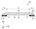
먼저 도 2를 참조하면, 한 실시예에 따른 윈도우 부재(200)는 베이스 부재(210) 및 제1 인쇄층(10)을 포함할 수 있다.Referring first to FIG. 2, the
베이스 부재(210)는 유리, 사파이어, 플라스틱 등의 절연 물질을 포함할 수 있다.The
단면 뷰에서, 베이스 부재(210)는 하부면(SF1) 및 상부면(SF2)을 포함할 수 있다. 하부면(SF1)은 표시 패널(100)을 향하는 면으로 대체로 평평할 수 있다. 상부면(SF2) 중 비투과 영역(BA)에 대응하는 상부면(SF2)은 휘어져 있을 수 있고, 투과 영역(TA)에 대응하는 상부면(SF2)은 대체로 평평하여 하부면(SF1)에 실질적으로 나란하게 연장되어 있을 수 있다. 즉, 하부면(SF1)과 투과 영역(TA)에 대응하는 상부면(SF2)은 제1방향(DR1) 및 제2방향(DR2)이 이루는 평면에 평행할 수 있다.In a sectional view, the
베이스 부재(210) 중 비투과 영역(BA)에 대응하는 부분의 두께는 베이스 부재(210)의 가장자리로 갈수록 점점 얇아질 수 있다. 베이스 부재(210) 중 투과 영역(TA)에 대응하는 부분은 실질적으로 일정한 두께를 가질 수 있다.The thickness of the portion of the
그러나 베이스 부재(210)의 단면 형태는 도 2에 도시한 바에 한정되는 것은 아니고, 상부면(SF2)도 하부면(SF1)과 같이 전체적으로 평평할 수도 있다. 이 경우, 베이스 부재(210)의 제3방향(DR3)의 두께는 전체적으로 균일할 수 있다.However, the cross-sectional shape of the
제1 인쇄층(10)은 윈도우 부재(200)의 비투과 영역(BA)에 대응하여 형성되어 있을 수 있다. 또한 제1 인쇄층(10)은 표시 장치(1000)의 표시 영역(DA)에 대응하며 외부로부터 표시 장치(1000)의 내부가 시인되는 것을 방지할 수 있다. 제1 인쇄층(10)은 흑색 또는 흰색일 수 있으나 이에 한정되지 않고, 유채색 또는 금속색 등 다양한 색을 가질 수 있다. 제1 인쇄층(10)은 차광 기능을 가질 수 있다.The
제1 인쇄층(10)은 색 구현을 위한 안료가 혼합된 아크릴계 수지, 에폭시계 수지, 폴리우레탄, 실리콘 등과 같은 수지 물질을 포함할 수 있다.The
제1 인쇄층(10)은 베이스 부재(210)의 하부면(SF1) 상에 직접 위치하여 하부면(SF1)과 접촉할 수 있다. 이에 따라, 본 실시예에서 제1 인쇄층(10)은 베이스 부재(210)의 하부면(SF1)을 따라 대체로 평평한 면을 가질 수 있다. 또한, 제1 인쇄층(10)과 베이스 부재(210) 사이에는 점착층, 필름 등의 다른 층이 존재하지 않는다.The
제1 인쇄층(10)은 베이스 부재(210)의 하부면(SF1) 상에 직접 인쇄되어 형성된 층이다. 제1 인쇄층(10)은 베이스 부재(210)의 하부면(SF1) 상에 스프레이, 증착 공정, 코팅 공정, 인쇄 공정 등의 다양한 방법으로 형성될 수 있다.The
제1 인쇄층(10)은 비투과 영역(BA)에 위치하는 제거부(11)를 포함할 수 있다. 제거부(11)는 도 2에 도시한 바와 같이 베이스 부재(210)의 하부면(SF1)까지 제1 인쇄층(10)이 제거되어 개구부를 이룰 수 있다. 이와 달리, 하부면(SF1)에 인접한 일부 제1 인쇄층(10)이 남아 있을 수도 있다.The
제거부(11)는 제1 인쇄층(10)의 패턴을 형성할 수 있다. 제거부(11)를 포함하는 제1 인쇄층(10)을 패터닝된 제1 인쇄층(10)이라 한다. 제1 인쇄층(10)은 레이저를 이용하여 패터닝될 수 있다. 따라서 제1 인쇄층(10)은 원하는 바에 따라 제거부(11)의 폭이 미세하게 패터닝될 수 있고, 제거부(11)의 폭(W1)을 최소화할 수 있다. 따라서 제1 인쇄층(10)의 디자인의 다양성 및 고급감을 높일 수 있다.The
제거부(11)의 폭(W1)은 대략 0.05 mm까지도 가능하다. 폭(W1)은 제1방향(DR1) 및 제2방향(DR2)에 평행한 평면 상에서의 폭을 의미한다.The width W1 of the
제1 인쇄층(10) 상에는 제2 인쇄층(20)이 위치할 수 있다. 제2 인쇄층(20)은 제1 인쇄층(10)과 다른 층에 위치할 수 있다. 즉, 제1 인쇄층(10)은 베이스 부재(210)와 제2 인쇄층(20) 사이에 위치할 수 있다.The
제2 인쇄층(20)의 색은 제1 인쇄층(10)의 색과 다를 수도 있고 같을 수도 있다. 예를 들어, 제2 인쇄층(20)은 제1 인쇄층(10)의 색과 다른 유채색 또는 금속색 등 다양한 색을 가질 수 있다. 제2 인쇄층(20)은 은(Ag) 등의 금속을 포함하여 빛을 반사할 수도 있다. 제2 인쇄층(20)은 반투명하여 입사되는 빛의 일부를 투과시킬 수 있다.The color of the
제2 인쇄층(20)은 색 구현을 위한 안료가 혼합된 아크릴계 수지, 에폭시계 수지, 폴리우레탄, 실리콘 등과 같은 수지 물질을 포함할 수 있다.The
제2 인쇄층(20)은 제1 인쇄층(10)의 제거부(11)와 중첩할 수 있다.The
제2 인쇄층(20)은 도 2에 도시한 바와 같이 제1 인쇄층(10)의 제거부(11) 안의 공간을 채우고 있을 수도 있고, 제1 인쇄층(10)의 제거부(11)의 적어도 일부를 채우고 있지 않을 수도 있다. 후자의 경우 제1 인쇄층(10)의 제거부(11)의 적어도 일부에는 공기가 채워져 있을 수 있다. 즉, 제거부(11)에서는 제2 인쇄층(20)과 베이스 부재(210)의 하부면(SF1) 사이는 이격되어 있을 수 있다.2, the
제2 인쇄층(20)은 제1 인쇄층(10)의 패터닝 후, 스프레이, 증착 공정, 코팅 공정, 인쇄 공정 등의 방법으로 형성될 수 있다.The
다른 실시예에 따르면, 제2 인쇄층(20)은 PET 등의 플라스틱 필름 상에 형성된 후 필름이 제1 인쇄층(10) 상에 부착되어 형성될 수도 있다. 이 경우, 제2 인쇄층(20)과 제1 인쇄층(10) 사이에는 PET 등의 필름이 더 위치하거나, PET 등의 필름과 제1 인쇄층(10) 사이에 제2 인쇄층(20)이 위치할 수도 있다.According to another embodiment, after the
제2 인쇄층(20) 상에는 적어도 하나의 제3 인쇄층이 더 위치할 수도 있다. 제3 인쇄층의 색, 형성 방법 등의 특징은 제2 인쇄층(20)과 유사할 수 있다. 예를 들어, 제3 인쇄층의 색은 제1 인쇄층(10) 및 제2 인쇄층(20)과 다른 색을 가질 수 있다.At least one third printing layer may be further positioned on the
도 3을 참조하면, 본 실시예에 따른 윈도우 부재(200a)는 도 2에 도시한 윈도우 부재(200)와 대부분 동일하나 베이스 부재(210)의 하부면(SF1)의 형태가 다를 수 있다. 본 실시예에서 베이스 부재(210)의 하부면(SF1)은 적어도 비투과 영역(BA)에서 휘어져 있을 수 있다. 이에 따라, 본 실시예에서 제1 인쇄층(10) 및 제2 인쇄층(20)은 베이스 부재(210)의 하부면(SF1)을 따라 휘어진 면을 가질 수 있다.Referring to FIG. 3, the
베이스 부재(210)의 하부면(SF1)의 휘어진 방향은 상부면(SF2)의 휘어진 방향과 같을 수 있다.The curved direction of the lower surface SF1 of the
베이스 부재(210)의 하부면(SF1)의 휘어진 곡률 반경은 상부면(SF2)의 휘어진 곡률 반경과 다를 수 있다. 예를 들어, 베이스 부재(210)의 하부면(SF1)의 휘어진 곡률 반경은 상부면(SF2)의 휘어진 곡률 반경보다 클 수 있다. 이 경우, 비투과 영역(BA)에 대응하는 베이스 부재(210)의 부분의 두께는 베이스 부재(210)의 가장자리로 갈수록 점점 얇아질 수 있다.The radius of curvature of the lower surface SF1 of the
다른 실시예에 따르면, 베이스 부재(210)의 하부면(SF1)의 휘어진 곡률 반경은 상부면(SF2)의 휘어진 곡률 반경과 실질적으로 동일할 수도 있다.According to another embodiment, the radius of curvature of the lower surface SF1 of the
다음, 앞에서 설명한 도면들과 함께 도 4 내지 도 10을 참조하여 한 실시예에 따른 표시 장치의 제조 방법에 대하여 설명한다.Next, a method of manufacturing a display device according to an exemplary embodiment will be described with reference to FIGS. 4 to 10 along with the aforementioned drawings.
도 4는 본 발명의 한 실시예에 따른 표시 장치의 윈도우 부재의 제조 방법의 순서도이고, 도 5는 본 발명의 한 실시예에 따른 표시 장치의 윈도우 부재의 제조 방법의 한 단계에서의 윈도우 부재의 평면도이고, 도 6은 도 5에 도시한 윈도우 부재를 Va-Vb 선을 따라 잘라 도시한 단면도이고, 도 7은 본 발명의 한 실시예에 따른 표시 장치의 윈도우 부재의 제조 방법의 한 단계에서의 윈도우 부재의 평면도이고, 도 8은 도 7에 도시한 윈도우 부재를 VIIa-VIIb 선을 따라 잘라 도시한 단면도이고, 도 9는 본 발명의 한 실시예에 따른 표시 장치의 윈도우 부재의 제조 방법의 한 단계에서의 윈도우 부재의 평면도이고, 도 10은 도 9에 도시한 윈도우 부재를 IXa-IXb 선을 따라 잘라 도시한 단면도이다.4 is a flowchart of a method of manufacturing a window member of a display device according to an embodiment of the present invention, and FIG. 5 is a window member of a method of manufacturing a window member of a display device according to an embodiment of the present invention FIG. 6 is a cross-sectional view of the window member shown in FIG. 5 taken along line Va-Vb, and FIG. 7 is a step in a method of manufacturing a window member of a display device according to an exemplary embodiment of the present invention. FIG. 8 is a plan view of a window member, and FIG. 8 is a cross-sectional view of the window member shown in FIG. 7 taken along line VIIa-VIIb, and FIG. 9 is a view of a method of manufacturing a window member of a display device according to an embodiment It is a top view of the window member in a step, and FIG. 10 is a cross-sectional view of the window member shown in FIG. 9 taken along line IXa-IXb.
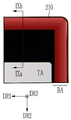
먼저 도 4 내지 도 6을 참조하면, 유리, 사파이어, 플라스틱 등의 절연 물질로 이루어진 베이스 부재(210)의 하부면(SF1) 상에 흑색, 흰색, 유채색, 또는 금속색 등의 색을 가지는 제1 인쇄층(10)을 형성한다(S40). 제1 인쇄층(10)은 베이스 부재(210)의 하부면(SF1) 상에 스프레이, 증착 공정, 코팅 공정, 인쇄 공정 등의 방법으로 형성될 수 있다. 제1 인쇄층(10)의 형성은 베이스 부재(210)의 하부면(SF1) 상에 직접 인쇄되고 이를 1차 인쇄라 한다.Referring first to FIGS. 4 to 6, a first having a color such as black, white, chromatic color, or metallic color on the lower surface SF1 of the
도 5를 참조하면, 제1 인쇄층(10)이 형성된 영역은 윈도우 부재(200)의 비투과 영역(BA)에 대응되고, 제1 인쇄층(10)이 형성되지 않은 영역은 투과 영역(TA)에 대응할 수 있다.Referring to FIG. 5, the area where the
다음 도 4, 도 7 및 도 8을 참조하면, 제1 인쇄층(10)에 레이저를 조사하여 제1 인쇄층(10)을 패터닝한다(S41). 레이저가 조사된 제1 인쇄층(10)의 일부가 제거되어 제거부(11)가 형성될 수 있다. 제거부(11)에서 제1 인쇄층(10)이 모두 제거되어 제거부(11)와 중첩하는 베이스 부재(210)의 하부면(SF1)이 노출되는 개구부가 형성될 수도 있고, 제거부(11)에서 하부면(SF1)과 인접한 제1 인쇄층(10)의 일부가 남을 수도 있다.Next, referring to FIGS. 4, 7 and 8, the
레이저를 이용한 패터닝을 통해 형성된 제1 인쇄층(10)의 제거부(11)의 폭(W1)은 대략 0.05 mm까지도 작게 할 수 있다.The width W1 of the
제거부(11)가 이루는 형태 및 배치는 다양할 수 있다. 예를 들어 도 7 및 도 8을 참조하면, 제1 인쇄층(10)이 가지는 복수의 제거부(11)의 폭(W1), 즉 제거부(11)의 사이즈가 위치에 따라 달라질 수 있다. 예를 들어, 평면 뷰에서 제거부(11)의 폭(W1)은 베이스 부재(210)의 가장자리에 가까워질수록 점차 커질 수 있으나, 제거부(11)의 배치 및 형태가 이에 한정되는 것은 아니다.The shape and arrangement of the
다음 도 4를 참조하면, 레이저 패터닝된 제1 인쇄층(10)이 형성된 베이스 부재(210)를 세정하여(S42) 그을음 입자 등의 불순물을 제거한다.Referring to FIG. 4, the
다음 도 4, 도 9 및 도 10을 참조하면, 패터닝된 제1 인쇄층(10) 상에 제1 인쇄층(10)의 색과 다른 유채색 또는 금속색 등 다양한 색을 가지는 제2 인쇄층(20)을 형성한다(S43). 도 9는 제2 인쇄층(20)의 색이 빨간색인 예를 도시한다.Next, referring to FIGS. 4, 9, and 10, a
제2 인쇄층(20)은 제1 인쇄층(10) 상에 스프레이, 증착 공정, 코팅 공정, 인쇄 공정 등의 방법으로 형성될 수 있다. 제2 인쇄층(20)의 형성은 베이스 부재(210)의 하부면(SF1) 상에 인쇄된 제1 인쇄층(10) 상에 인쇄되고 이를 2차 인쇄라 한다.The
제2 인쇄층(20)은 제1 인쇄층(10)의 제거부(11)와 중첩하므로 베이스 부재(210)의 상부면(SF2) 쪽에서 보았을 때 제1 인쇄층(10)의 제거부(11)는 제1 인쇄층(10)과 다른 색으로 시인될 수 있다.Since the
이와 달리, 제1 인쇄층(10) 상에 제2 인쇄층(20)을 직접 형성하지 않고, PET 등의 별도 필름 상에 제2 인쇄층(20)을 스프레이, 증착 공정, 코팅 공정, 인쇄 공정 등의 방법으로 형성한 후, 필름을 제1 인쇄층(10) 상에 부착할 수도 있다.Alternatively, instead of directly forming the
본 실시예에 따르면, 복수의 제거부(11)의 배치와 모양 등의 형태와 제2 인쇄층(20)의 색을 조절하여 윈도우 부재(200)의 비투과 영역(BA)의 디자인을 다양하게 할 수 있고 고급감을 높일 수 있다. 특히, 제1 인쇄층(10)을 레이저를 이용하여 패터닝하여 제거부(11)를 형성하므로 제거부(11)의 폭을 미세하게 할 수 있고 다양한 형상으로 용이하게 구현할 수 있어 윈도우 부재(200)의 비투과 영역(BA)의 디자인을 더욱 다양하게 하고 고급감을 높일 수 있다.According to this embodiment, the design of the non-transmissive area BA of the
제2 인쇄층(20)의 형성 이후 제2 인쇄층(20) 상에 적어도 하나의 제3 인쇄층을 더 형성할 수도 있다. 제3 인쇄층은 제2 인쇄층(20) 상에 스프레이, 증착 공정, 코팅 공정, 인쇄 공정 등의 방법으로 직접 형성될 수도 있고, 별도의 필름 상에 제3 인쇄층을 형성한 후 필름을 제2 인쇄층(20) 상에 부착시킬 수도 있다.After the
이와 같이 제1 인쇄층(10) 및 제2 인쇄층(20)이 형성된 윈도우 부재를 앞에서 설명한 표시 패널(100)과 합착하여 한 실시예에 따른 표시 장치를 제조할 수 있다.The display device according to an embodiment may be manufactured by bonding the window member on which the
다음, 도 11을 참조하여 본 발명의 한 실시예에 따른 표시 장치의 윈도우 부재에 대하여 설명한다.Next, a window member of the display device according to an exemplary embodiment will be described with reference to FIG. 11.
도 11은 본 발명의 한 실시예에 따른 표시 장치의 윈도우 부재의 단면도이다.11 is a cross-sectional view of a window member of a display device according to an exemplary embodiment.
도 11을 참조하면, 본 실시예에 따른 표시 장치의 윈도우 부재는 앞에서 설명한 실시예와 대부분 동일하나, 제1 인쇄층(10) 상에 제2 인쇄층(20a)이 위치하고, 제2 인쇄층(20a)과 제1 인쇄층(10) 사이에는 점착층(25) 및 필름(26)이 위치할 수 있다. 제2 인쇄층(20a)은 앞에서 설명한 제2 인쇄층(20)의 특징과 동일한 특징을 가질 수 있다. 필름(26)은 PET 등의 플라스틱 필름일 수 있다.Referring to FIG. 11, the window member of the display device according to the present embodiment is mostly the same as the above-described embodiment, but the
다른 실시예에 따르면, 단면 뷰에서 제2 인쇄층(20a)과 필름(26)의 위치는 바뀔 수도 있다.According to another embodiment, the positions of the second printed
도 11에 도시한 실시예에서, 제1 인쇄층(10)의 제거부(11) 안은 공기로 채워져 있을 수 있다.In the embodiment shown in FIG. 11, the inside of the
도 11에 도시한 실시예에 따른 표시 장치의 윈도우 부재의 제조 방법에 대하여 설명하면, 앞에서 설명한 도 4 내지 도 10에 도시한 실시예에 따른 윈도우 부재의 제조 방법과 대부분 동일하나, 제1 인쇄층(10)에 대한 레이저 패터닝 이후의 단계가 다를 수 있다.The method of manufacturing the window member of the display device according to the embodiment illustrated in FIG. 11 is mostly the same as the method of manufacturing the window member according to the embodiment shown in FIGS. 4 to 10 described above, but the first printing layer The steps after laser patterning for (10) may be different.
도 10에 도시한 단계와 달리, 별도로 마련된 필름(26) 위에 제2 인쇄층(20a)을 형성한 후, 제2 인쇄층(20a)이 형성된 필름(26)을 제1 인쇄층(10) 위에 점착층(25)을 통해 부착시킬 수 있다.Unlike the steps illustrated in FIG. 10, after forming the
다음 도 12를 참조하여 한 실시예에 따른 표시 장치의 윈도우 부재의 인쇄층의 다양한 패턴의 예에 대하여 설명한다.Next, examples of various patterns of the printed layer of the window member of the display device according to an exemplary embodiment will be described with reference to FIG. 12.
도 12는 본 발명의 한 실시예에 따른 표시 장치의 윈도우 부재의 인쇄층의 패턴의 다양한 예를 도시한다.12 illustrates various examples of patterns of a printed layer of a window member of a display device according to an embodiment of the present invention.
도 12를 참조하면, 본 발명의 한 실시예에 따른 윈도우 부재(200)의 제1 인쇄층(10)의 제거부(11)의 형태에 따른 제1 인쇄층(10)의 패턴은 다양할 수 있다. 예를 들어, 제1 인쇄층(10)은 도 12의 표에 도시한 다양한 패턴을 이루는 제거부(11)를 가질 수 있고, 이러한 패턴은 제1방향(DR1) 및/또는 제2방향(DR2)으로 반복되며 배치될 수 있다.Referring to FIG. 12, the pattern of the
이상에서 본 발명의 실시예에 대하여 상세하게 설명하였지만 본 발명의 권리범위는 이에 한정되는 것은 아니고 다음의 청구범위에서 정의하고 있는 본 발명의 기본 개념을 이용한 당업자의 여러 변형 및 개량 형태 또한 본 발명의 권리범위에 속하는 것이다.Although the embodiments of the present invention have been described in detail above, the scope of the present invention is not limited thereto, and various modifications and improvements of those skilled in the art using the basic concept of the present invention defined in the following claims are also provided. It belongs to the scope of rights.
10: 제1 인쇄층
11: 제거부
20: 제2 인쇄층
100: 표시 패널
110: 기판
120: 봉지층
150: 케이스 부재
200: 윈도우 부재
210: 베이스 부재
500: 가요성 인쇄 회로 기판
600: 인쇄 회로 기판10: first printing layer
11: remover
20: second printing layer
100: display panel
110: substrate
120: sealing layer
150: case absence
200: window absent
210: base member
500: flexible printed circuit board
600: printed circuit board
Claims (25)
상기 표시 영역에 대응하는 투과 영역 및 상기 주변 영역에 대응하는 비투과 영역을 포함하는 윈도우 부재를 포함하고,
상기 윈도우 부재는 베이스 부재 및 상기 베이스 부재의 제1면 상에 직접 형성되어 있는 제1 인쇄층을 포함하고,
상기 제1 인쇄층은 제거부를 포함하고,
상기 제거부는 상기 비투과 영역에 위치하는
표시 장치.A display panel including a display area including a plurality of pixels and a peripheral area located outside the display area, and
And a window member including a transmissive area corresponding to the display area and a non-transmissive area corresponding to the peripheral area,
The window member includes a base member and a first printing layer formed directly on the first surface of the base member,
The first printing layer includes a removing portion,
The removal unit is located in the non-transmissive area
Display device.
상기 제1 인쇄층 상에 위치하는 제2 인쇄층을 더 포함하고,
상기 제2 인쇄층의 색은 상기 제1 인쇄층의 색과 다른
표시 장치.In claim 1,
Further comprising a second print layer located on the first print layer,
The color of the second printed layer is different from the color of the first printed layer
Display device.
상기 제1 인쇄층의 색은 흑색이고,
상기 제2 인쇄층의 색은 유채색 또는 금속색인
표시 장치.In claim 2,
The color of the first printed layer is black,
The color of the second printed layer is chromatic or metallic
Display device.
상기 제2 인쇄층은 상기 제거부와 중첩하는 표시 장치.In claim 2,
The second printing layer is a display device overlapping the removal unit.
상기 제2 인쇄층은 상기 제1 인쇄층과 접촉하는 부분을 포함하고,
상기 제2 인쇄층은 상기 제거부 안의 공간을 채우고 있는
표시 장치.In claim 4,
The second printing layer includes a portion in contact with the first printing layer,
The second printing layer fills the space in the removal portion
Display device.
상기 제거부 안의 공간의 적어도 일부는 상기 제2 인쇄층으로 채워져 있지 않은 표시 장치.In claim 4,
A display device in which at least part of the space in the removal portion is not filled with the second printed layer.
상기 제2 인쇄층과 상기 제1 인쇄층 사이에 위치하는 필름을 더 포함하는 표시 장치.In claim 6,
And a film positioned between the second printing layer and the first printing layer.
상기 제2 인쇄층과 상기 제1 인쇄층 사이에 위치하는 점착층을 더 포함하는 표시 장치.In claim 7,
And an adhesive layer positioned between the second printed layer and the first printed layer.
상기 제1면은 상기 표시 패널을 향하는 면인 표시 장치.In claim 1,
The first surface is a display device facing the display panel.
상기 제거부는 레이저 패터닝으로 형성된 표시 장치.In claim 1,
The removal unit is a display device formed by laser patterning.
상기 표시 영역에 대응하는 투과 영역 및 상기 주변 영역에 대응하는 비투과 영역을 포함하는 윈도우 부재를 포함하고,
상기 윈도우 부재는, 베이스 부재 및 상기 베이스 부재의 제1면과 접촉하는 제1 인쇄층, 그리고 상기 제1 인쇄층과 다른 층에 위치하는 제2 인쇄층을 포함하고,
상기 제1 인쇄층은, 상기 제1면까지 상기 제1 인쇄층이 제거되어 있는 개구부를 포함하고,
상기 제2 인쇄층은 상기 개구부와 중첩하는
표시 장치.A display panel including a display area including a plurality of pixels and a peripheral area located outside the display area, and
And a window member including a transmissive area corresponding to the display area and a non-transmissive area corresponding to the peripheral area,
The window member includes a base member, a first printing layer in contact with the first surface of the base member, and a second printing layer positioned on a different layer from the first printing layer,
The first printing layer includes an opening in which the first printing layer is removed to the first surface,
The second printing layer overlaps the opening
Display device.
상기 제2 인쇄층의 색은 상기 제1 인쇄층의 색과 다른 표시 장치.In claim 11,
The color of the second printed layer is different from that of the first printed layer.
상기 제1 인쇄층의 색은 흑색이고,
상기 제2 인쇄층의 색은 유채색 또는 금속색인
표시 장치.In claim 12,
The color of the first printed layer is black,
The color of the second printed layer is chromatic or metallic
Display device.
상기 제2 인쇄층은 상기 제1 인쇄층과 접촉하는 부분을 포함하고,
상기 제2 인쇄층은 상기 제거부 안의 공간을 채우고 있는
표시 장치.In claim 11,
The second printing layer includes a portion in contact with the first printing layer,
The second printing layer fills the space in the removal portion
Display device.
상기 제거부 안의 공간의 적어도 일부는 상기 제2 인쇄층으로 채워져 있지 않은 표시 장치.In claim 11,
A display device in which at least part of the space in the removal portion is not filled with the second printed layer.
상기 제2 인쇄층과 상기 제1 인쇄층 사이에 위치하는 필름을 더 포함하는 표시 장치.In claim 15,
And a film positioned between the second printing layer and the first printing layer.
상기 제2 인쇄층과 상기 제1 인쇄층 사이에 위치하는 점착층을 더 포함하는 표시 장치.In claim 16,
And an adhesive layer positioned between the second printed layer and the first printed layer.
상기 제1면은 상기 표시 패널을 향하는 면인 표시 장치.In claim 11,
The first surface is a display device facing the display panel.
상기 제거부는 레이저 패터닝으로 형성된 표시 장치.In claim 11,
The removal unit is a display device formed by laser patterning.
상기 제1 인쇄층을 레이저를 이용해 패터닝하여 제거부를 형성하는 단계,
상기 제거부가 형성된 상기 제1 인쇄층 상에 제2 인쇄층을 형성하는 단계,
복수의 화소를 포함하는 표시 패널을 마련하는 단계, 그리고
상기 제1 인쇄층 및 상기 제2 인쇄층이 형성된 상기 베이스 부재와 상기 표시 패널을 합착하는 단계
를 포함하고,
상기 제2 인쇄층은 상기 제거부와 중첩하는
표시 장치의 제조 방법.Forming a first printed layer on the first surface of the non-transmissive area of the base member,
Patterning the first printed layer using a laser to form a removal portion,
Forming a second printing layer on the first printing layer on which the removal unit is formed,
Providing a display panel including a plurality of pixels, and
Bonding the base member and the display panel on which the first printing layer and the second printing layer are formed
Including,
The second printing layer overlaps the removal portion
Method for manufacturing a display device.
상기 제1면 상에 상기 제1 인쇄층을 형성하는 단계는, 증착, 스프레이, 코팅, 인쇄 중 하나를 이용하는 표시 장치의 제조 방법.In claim 20,
The forming of the first printing layer on the first surface may be performed by one of deposition, spraying, coating, and printing.
상기 제1 인쇄층 상에 상기 제2 인쇄층을 형성하는 단계는, 증착, 스프레이, 코팅, 인쇄 중 하나를 이용하는 표시 장치의 제조 방법.In claim 20,
The forming of the second printing layer on the first printing layer is a method of manufacturing a display device using one of deposition, spraying, coating, and printing.
상기 제1 인쇄층 상에 상기 제2 인쇄층을 형성하는 단계는
필름 위에 상기 제2 인쇄층을 형성하는 단계, 그리고
상기 필름을 상기 제1 인쇄층 상에 부착시키는 단계
를 포함하는 표시 장치의 제조 방법.In claim 20,
The step of forming the second print layer on the first print layer
Forming the second printing layer on a film, and
Attaching the film on the first printed layer
Method for manufacturing a display device comprising a.
상기 제1 인쇄층에 상기 제거부를 형성하는 단계와 상기 제2 인쇄층을 형성하는 단계 사이에, 상기 베이스 부재를 세정하는 단계를 더 포함하는 표시 장치의 제조 방법.In claim 20,
A method of manufacturing a display device further comprising the step of cleaning the base member between the step of forming the removal portion on the first print layer and the step of forming the second print layer.
상기 제2 인쇄층의 색은 상기 제1 인쇄층의 색과 다른 표시 장치의 제조 방법.In claim 20,
A method of manufacturing a display device in which the color of the second printed layer is different from the color of the first printed layer.
Priority Applications (4)
| Application Number | Priority Date | Filing Date | Title |
|---|---|---|---|
| KR1020190001348A KR20200085402A (en) | 2019-01-04 | 2019-01-04 | Display device including window member and manufacturing method thereof |
| US16/723,960 US11528813B2 (en) | 2019-01-04 | 2019-12-20 | Display device including window member and manufacturing method thereof |
| TW108148412A TW202042196A (en) | 2019-01-04 | 2019-12-30 | Display device including window member |
| CN202010003228.1A CN111509002A (en) | 2019-01-04 | 2020-01-02 | Display device |
Applications Claiming Priority (1)
| Application Number | Priority Date | Filing Date | Title |
|---|---|---|---|
| KR1020190001348A KR20200085402A (en) | 2019-01-04 | 2019-01-04 | Display device including window member and manufacturing method thereof |
Publications (1)
| Publication Number | Publication Date |
|---|---|
| KR20200085402A true KR20200085402A (en) | 2020-07-15 |
Family
ID=71404575
Family Applications (1)
| Application Number | Title | Priority Date | Filing Date |
|---|---|---|---|
| KR1020190001348A KR20200085402A (en) | 2019-01-04 | 2019-01-04 | Display device including window member and manufacturing method thereof |
Country Status (4)
| Country | Link |
|---|---|
| US (1) | US11528813B2 (en) |
| KR (1) | KR20200085402A (en) |
| CN (1) | CN111509002A (en) |
| TW (1) | TW202042196A (en) |
Families Citing this family (1)
| Publication number | Priority date | Publication date | Assignee | Title |
|---|---|---|---|---|
| KR102580292B1 (en) * | 2018-05-29 | 2023-09-19 | 삼성디스플레이 주식회사 | Display device, method for fabricating the device and laser processing apparatus for fabricating the device |
Family Cites Families (20)
| Publication number | Priority date | Publication date | Assignee | Title |
|---|---|---|---|---|
| JP2003205375A (en) | 2002-01-09 | 2003-07-22 | Shiseido Co Ltd | Method of forming engraved letter on label with laser beam |
| KR101161521B1 (en) | 2010-12-02 | 2012-07-02 | 서울옵토디바이스주식회사 | Method for forming isolation pattern of wafer using laser marking and system for measuring electroluminescence thereof |
| KR101772077B1 (en) * | 2010-12-28 | 2017-08-28 | 엘지전자 주식회사 | Window, fabaricating method thereof, and portable terminal having the same |
| US10061356B2 (en) * | 2011-06-30 | 2018-08-28 | Samsung Display Co., Ltd. | Flexible display panel and display apparatus including the flexible display panel |
| KR20140003046A (en) | 2012-06-29 | 2014-01-09 | 엘지이노텍 주식회사 | Touch window and fabricating method of the same, and lcd using the same |
| WO2014069740A1 (en) * | 2012-11-02 | 2014-05-08 | Samsung Electronics Co., Ltd. | Window member for a portable terminal and method for fabricating same |
| KR20140082432A (en) * | 2012-12-24 | 2014-07-02 | 삼성전기주식회사 | Window glass having inlay printing area in Bezel and Method for manufacturing the window glass |
| US9890074B2 (en) * | 2013-02-21 | 2018-02-13 | Htc Corporation | Electronic device, glass cover and method of manufacturing glass cover |
| KR101336934B1 (en) * | 2013-03-05 | 2013-12-03 | 크루셜텍 (주) | Cover glass and method of manufacturing the same |
| US9769938B2 (en) * | 2013-03-12 | 2017-09-19 | Samsung Electronics Co., Ltd. | Window member and method of manufacturing the same |
| JP6387105B2 (en) * | 2014-02-05 | 2018-09-05 | サムウォン エスティー | Transparent cover for electronic equipment |
| KR101501427B1 (en) | 2014-11-20 | 2015-03-12 | 주식회사 에스에스뉴테크 | Cover window of mobile device and manufacturing method thereof |
| KR102334796B1 (en) * | 2015-07-10 | 2021-12-07 | 삼성디스플레이 주식회사 | Display apparatus |
| KR102419181B1 (en) * | 2015-09-16 | 2022-07-11 | 삼성디스플레이 주식회사 | Display device and method of manufacturing window member |
| KR102500048B1 (en) * | 2015-11-20 | 2023-02-16 | 삼성디스플레이 주식회사 | Window substrate and display apparatus including the same |
| KR101760731B1 (en) | 2015-12-22 | 2017-07-25 | 주식회사 씨아이씨티 | Glass micro pattern forming method and micro pattern structure thereof |
| EP3210948B1 (en) * | 2016-02-29 | 2019-12-04 | Schott Ag | Coated glass or glass ceramic article |
| KR102516344B1 (en) * | 2016-06-21 | 2023-04-03 | 삼성전자주식회사 | Cover window and electronic device including the same |
| JP6574873B1 (en) * | 2018-05-25 | 2019-09-11 | 株式会社三和スクリーン銘板 | Panel member manufacturing method |
| KR102640704B1 (en) * | 2018-08-02 | 2024-02-27 | 삼성전자 주식회사 | A cover class and an elelctronic apparturs compsrising the same |
-
2019
- 2019-01-04 KR KR1020190001348A patent/KR20200085402A/en not_active Application Discontinuation
- 2019-12-20 US US16/723,960 patent/US11528813B2/en active Active
- 2019-12-30 TW TW108148412A patent/TW202042196A/en unknown
-
2020
- 2020-01-02 CN CN202010003228.1A patent/CN111509002A/en active Pending
Also Published As
| Publication number | Publication date |
|---|---|
| US20200221588A1 (en) | 2020-07-09 |
| CN111509002A (en) | 2020-08-07 |
| US11528813B2 (en) | 2022-12-13 |
| TW202042196A (en) | 2020-11-16 |
Similar Documents
| Publication | Publication Date | Title |
|---|---|---|
| JP6811353B2 (en) | Display device, glass substrate and glass substrate manufacturing method | |
| KR102607379B1 (en) | Display device and method of manufacturing of the same | |
| TWI476656B (en) | Touch panel and manufacturing method thereof | |
| KR102084110B1 (en) | Cover window for display device, display device comprising the same, and mathod for manufacturing the same | |
| US10031367B2 (en) | Display with inverted thin-film-transistor layer | |
| US9429988B2 (en) | Touch screen panel | |
| US11043656B2 (en) | Display device incorporating a scattering pattern | |
| US20120268402A1 (en) | Touch display panel | |
| US20120218219A1 (en) | Displays with minimized borders | |
| JP7258520B2 (en) | Display device | |
| KR101422746B1 (en) | Narrow bezel type display device | |
| US10804486B2 (en) | Display device | |
| KR20200022554A (en) | Display device and method of manufacturing display device | |
| US20200202788A1 (en) | Display device | |
| US10302844B2 (en) | Display with backlight recycling structures | |
| KR102211207B1 (en) | Electronic product | |
| KR102065537B1 (en) | Display Device | |
| KR20200085402A (en) | Display device including window member and manufacturing method thereof | |
| CN112860126A (en) | Display device, touch display panel, touch panel and manufacturing method thereof | |
| US11579473B2 (en) | Display device having uniform reflectance | |
| CN112736115A (en) | Method for manufacturing circuit board and display device comprising circuit board | |
| KR20210086857A (en) | Display apparatus |
Legal Events
| Date | Code | Title | Description |
|---|---|---|---|
| A201 | Request for examination | ||
| E902 | Notification of reason for refusal | ||
| E90F | Notification of reason for final refusal |