EP3392696A1 - Oscillating structure with reduced dynamic deformation, optical device including the oscillating structure, and method of manufacturing the oscillating structure - Google Patents
Oscillating structure with reduced dynamic deformation, optical device including the oscillating structure, and method of manufacturing the oscillating structure Download PDFInfo
- Publication number
- EP3392696A1 EP3392696A1 EP18163484.1A EP18163484A EP3392696A1 EP 3392696 A1 EP3392696 A1 EP 3392696A1 EP 18163484 A EP18163484 A EP 18163484A EP 3392696 A1 EP3392696 A1 EP 3392696A1
- Authority
- EP
- European Patent Office
- Prior art keywords
- coupling
- torsional elastic
- elastic element
- regions
- plane
- Prior art date
- Legal status (The legal status is an assumption and is not a legal conclusion. Google has not performed a legal analysis and makes no representation as to the accuracy of the status listed.)
- Granted
Links
Images

Classifications
-
- G—PHYSICS
- G02—OPTICS
- G02B—OPTICAL ELEMENTS, SYSTEMS OR APPARATUS
- G02B26/00—Optical devices or arrangements for the control of light using movable or deformable optical elements
- G02B26/08—Optical devices or arrangements for the control of light using movable or deformable optical elements for controlling the direction of light
- G02B26/0816—Optical devices or arrangements for the control of light using movable or deformable optical elements for controlling the direction of light by means of one or more reflecting elements
- G02B26/0833—Optical devices or arrangements for the control of light using movable or deformable optical elements for controlling the direction of light by means of one or more reflecting elements the reflecting element being a micromechanical device, e.g. a MEMS mirror, DMD
-
- G—PHYSICS
- G02—OPTICS
- G02B—OPTICAL ELEMENTS, SYSTEMS OR APPARATUS
- G02B26/00—Optical devices or arrangements for the control of light using movable or deformable optical elements
- G02B26/08—Optical devices or arrangements for the control of light using movable or deformable optical elements for controlling the direction of light
-
- B—PERFORMING OPERATIONS; TRANSPORTING
- B81—MICROSTRUCTURAL TECHNOLOGY
- B81B—MICROSTRUCTURAL DEVICES OR SYSTEMS, e.g. MICROMECHANICAL DEVICES
- B81B3/00—Devices comprising flexible or deformable elements, e.g. comprising elastic tongues or membranes
- B81B3/0064—Constitution or structural means for improving or controlling the physical properties of a device
- B81B3/0067—Mechanical properties
- B81B3/007—For controlling stiffness, e.g. ribs
-
- G—PHYSICS
- G02—OPTICS
- G02B—OPTICAL ELEMENTS, SYSTEMS OR APPARATUS
- G02B26/00—Optical devices or arrangements for the control of light using movable or deformable optical elements
- G02B26/08—Optical devices or arrangements for the control of light using movable or deformable optical elements for controlling the direction of light
- G02B26/0816—Optical devices or arrangements for the control of light using movable or deformable optical elements for controlling the direction of light by means of one or more reflecting elements
-
- G—PHYSICS
- G02—OPTICS
- G02B—OPTICAL ELEMENTS, SYSTEMS OR APPARATUS
- G02B26/00—Optical devices or arrangements for the control of light using movable or deformable optical elements
- G02B26/08—Optical devices or arrangements for the control of light using movable or deformable optical elements for controlling the direction of light
- G02B26/10—Scanning systems
-
- G—PHYSICS
- G02—OPTICS
- G02B—OPTICAL ELEMENTS, SYSTEMS OR APPARATUS
- G02B26/00—Optical devices or arrangements for the control of light using movable or deformable optical elements
- G02B26/08—Optical devices or arrangements for the control of light using movable or deformable optical elements for controlling the direction of light
- G02B26/10—Scanning systems
- G02B26/105—Scanning systems with one or more pivoting mirrors or galvano-mirrors
-
- B—PERFORMING OPERATIONS; TRANSPORTING
- B81—MICROSTRUCTURAL TECHNOLOGY
- B81B—MICROSTRUCTURAL DEVICES OR SYSTEMS, e.g. MICROMECHANICAL DEVICES
- B81B2201/00—Specific applications of microelectromechanical systems
- B81B2201/04—Optical MEMS
- B81B2201/042—Micromirrors, not used as optical switches
Definitions
- the present invention relates to an oscillating structure, an optical device including the oscillating structure, and a method of manufacturing the oscillating structure.
- the oscillating structure is designed to reduce the dynamic deformation of a moving (oscillating) mass belonging to said oscillating structure.
- the moving mass carries a reflective layer and the oscillating structure forms, at least in part, a micro-mirror.
- Micromechanical mirror structures made at least partially from semiconductor materials and fabricated using microelectromechanical systems (MEMS) technology are known.
- MEMS reflectors are designed to receive an optical beam and to change the propagation direction thereof, periodically or near periodically.
- MEMS reflectors include moving elements made from planar supports bearing reflective elements, the positions of which in space are controlled electrically using appropriate oscillation control signals.
- controlling the position of the reflective element is particularly important to enable a portion of space to be scanned with an optical beam falling on the mirror.
- controlling the position of the reflective element is of key importance for resonant MEMS reflectors, in which, when in use, the planar support is oscillated substantially periodically about an idle position.
- the oscillation frequency is as close as possible to the resonance frequency of the planar support in order to maximize the angular distance covered by the reflective element during each oscillation, thereby maximizing the size of the portion of space scanned.
- the high oscillation frequency causes accelerations of the planar support. Since the planar support is usually a thin layer having a circular or oval shape, the moment of inertia thereof and the limited rigidity cause a dynamic deformation, which results in a deformation of the planar support and of the reflective element.
- the applicant has determined that, for oscillation frequencies greater than 15 kHz and in the case of planar supports with a diameter exceeding 1 mm, even a deformation of a few tenths of nanometres (greater than 60 nm) of the reflective element degrades the optical performance of the MEMS reflector, causing aberrations in the projected image.
- the purpose of the present invention is to at least partially address the problems affecting known micromechanical mirror structures.
- the present invention is intended to provide an oscillating structure with reduced dynamic deformation, an optical device including the oscillating structure, and a method for manufacturing the oscillating structure with reduced dynamic deformation.
- the present invention provides an oscillating structure, an optical device including the oscillating structure, and a method of manufacturing the oscillating structure, as defined in the attached claims.
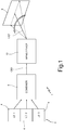
- Figure 1 shows a MEMS projection system 1 of a known type that includes a light source 2 formed for example by a plurality of laser diodes (LD) 4, each of which emits electromagnetic radiation at a corresponding wavelength.
- LD laser diodes
- Figure 1 shows three LDS 4, each of which emits radiation respectively in the red range (620-750 nm), green range (495-570 nm) and blue range (450-475 nm).
- the MEMS projection system 1 also includes a combiner 6, a MEMS device 10 (in particular an oscillating structure such as a micro-mirror), and a screen 8.
- the combiner 6 is arranged downstream of the light source 2, such as to receive the electromagnetic radiation emitted by the LDs 4 to form a single optical beam OBI, obtained by combining said electromagnetic radiation.
- the combiner 6 is also designed to direct the optical beam OB1 towards the MEMS device 10.
- the MEMS device 10 which is described in greater detail below, is in turn designed to generate a reflected optical beam OB2 and to send the reflected optical beam OB2 to the screen 8, to enable the formation of images on the screen 8.
- the MEMS device 10 is designed to vary the spatial orientation of the axis of the reflected optical beam OB2 over time such as to periodically scan portions of the screen 8.
- the reflected optical beam OB2 performs a linear scan of a portion of the screen 8, and potentially all of same.
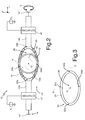
- FIG. 1 shows an embodiment of the MEMS device 10 according to an aspect of the present invention, in particular an oscillating structure such as a micromechanical mirror structure, or micro-mirror.
- the MEMS device is made using MEMS techniques from the semiconductor industry.
- the MEMS device 10 includes a static support body 14, in particular made of semiconductor material, that includes first and second fastenings regions 14', 14".
- the MEMS device 10 is shown in an orthogonal reference system formed by three Cartesian axes X, Y, Z that are orthogonal to one another. An axis H parallel to the axis Z of the reference system is also provided.
- the first and second fastenings regions 14', 14'' are arranged diametrically opposite one another about the axis H and are aligned with one another along an axis 0 parallel to the axis X.
- the static support body 14 defines a cavity 15.
- the MEMS device 10 also includes a moving mass 12 that is linked to the first and second fastenings regions 14', 14'' and is also suspended above the cavity 15.
- the moving mass 12, when idle, is substantially parallel to a horizontal plane XY.
- the moving mass 12 has a central portion 12a that is for example circular in the plan view (in the horizontal plane XY) and that is for example between 50 ⁇ m and 200 ⁇ m thick and that has a diameter of between 1 mm and 2 mm, and a mirror layer 16 that lies on the central portion 12a and that is for example between 0.05 ⁇ m and 0.3 ⁇ m thick.
- the mirror layer 16 incorporates a material with high reflectivity for the light radiation to be projected, for example aluminium or gold.
- Elastic elements 12b, 12c in particular torsional elastic elements, that are elongate (arm-shaped) extend from opposing portions of the central portion 12a, in the horizontal plane XY.
- the elastic elements 12b, 12c lie primarily and in particular a long the axis of rotation 0, passing through the geometric centre of the moving mass 12, which thus forms an axis of rotation for the moving mass 12.
- the thickness of the elastic elements 12b, 12c is the same as the thickness of the central portion 12a.
- said elastic elements may be thicker or thinner than the central portion 12a as required and as a function of the design parameters, such as the rigidity of the elastic elements 12b, 12c.
- the central portion 12a is coupled to the fastening regions 14', 14'' respectively by the elastic elements 12b, 12c, which enable the rotation of the central portion 12a outside the horizontal plane XY about the axis of rotation 0.
- the elastic elements 12b, 12c extend longitudinally along the axis X and the length of same along said axis X is greater than the corresponding width (along the axis Y on the horizontal plane XY) and than the corresponding thickness along the axis Z (vertical axis).
- the length, width and thickness of the elastic elements 12b, 12c are determined as a function of the desired torsional rigidity of same, in a known manner and not covered by the present invention.
- actuation of the MEMS device 10 involves, in a known manner, the twisting of the elastic elements 12b, 12c and the consequent rotation of the moving mass 12 outside the horizontal plane XY around the axis of rotation 0, as a function of the desired movement to reflect the incident light beam towards the outside of the MEMS device 10.
- the moving mass 12 can be actuated in rotation with an oscillating movement at the mechanical resonance frequency of same, in order to maximize the range of the movement thereof.
- the elastic elements 12b, 12c and the central portion 12a are not in direct contact with one another.
- the MEMS device 10 also includes a coupling structure 20 illustrated separately in Figure 3 according to a possible embodiment.
- the shape of the coupling structure 20 in the plan view may for example be oval, elliptical, quadrangular with bevelled corners, generically polygonal or polygonal with bevelled corners.
- the coupling structure 20 includes an annular portion 21 that contains one or more through-hole apertures 26.
- the thickness along Z of the coupling structure 20 is in particular uniform along the entire extension of the coupling structure 20, and is for example between 50 ⁇ m and 200 ⁇ m.
- the thickness of the coupling structure 20 need not be uniform along the entire extension of the coupling structure 20. In this case, the thicknesses are nonetheless symmetrical about the axis of rotation 0.
- the coupling structure 20 lie on a first lying plane that is different from, but parallel to, a second lying plane on which the central portion 12a and the elastic elements 12b, 12c lie.
- the first and second lying planes are parallel to the plane XY. More specifically, the coupling structure 20 lies beneath (along the axis Z) the central portion 12a and the elastic elements 12b, 12c.
- the coupling structure 20 is therefore vertically (i.e., along Z axis) staggered with respect to the central portion 12a and the elastic elements 12b, 12c.
- the central portion 12a and the elastic elements 12b, 12c are not mechanically connected to one another (i.e., are not in direct contact) when observed on the first lying plane.
- the coupling structure 20 is designed to mechanically couple the central portion 12a and the elastic elements 12b, 12c together on a different lying plane (second lying plane). There are coupling interface regions between the first and second lying planes, as shown in Figure 8 and described with reference to said figure.
- the elastic elements 12b, 12c and the central portion 12a are coupled together mechanically only by the coupling structure 20.
- the elastic elements 12b, 12c are coupled to the coupling structure 20 at the first regions 22a, 22b of the coupling structure 20, diametrically opposite one another about the axis H and aligned with one another along the axis 0.
- the central portion 12a is coupled to the coupling structure 20 at the second regions 24a, 24b of the coupling structure 20, diametrically opposite one another about the axis H and aligned with one another along an axis K perpendicular to the axis 0. Consequently, the regions 22a, 22b, 24a, 24b are arranged such as to maximize the distance between same.
- the regions 22a, 22b, 24a, 24b are arranged at the vertices of a cross formed by the minor axis and the major axis of the ellipse.
- the regions 22a, 22b, 24a, 24b include the midpoints of the large and small sides of said quadrangular coupling structure 20.
- the coupling structure 20 is designed such that the outer edges of the coupling structure 20, at the second regions 24a, 24b, are arranged above the central portion 12a, and in particular coincide with the respective outer edge portions of the central portion 12a.
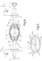
- FIG 4 shows a MEMS device 30 according to another embodiment of the present invention. Elements of the MEMS device 30 that are common with the MEMS device 10 in Figure 1 are identified using the same reference signs, and are not further described.
- the MEMS device 30 includes a coupling structure 32 that is similar to the coupling structure 20 and includes, in addition to the annular portion 21 (already described with reference to the coupling structure 20 and identified here using the same reference sign), a support portion 34 (in this case beam shaped) that is arranged inside the annular portion 21 symmetrically about the axis of rotation 0.
- the support portion 34 is formed from the same part as the annular portion 21, forming a one-piece structure.
- the support portion 34 is connected to the annular portion 21 at the first regions 22a, 22b of the coupling structure 32.
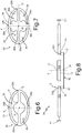
- the support portion 34 is substantially rectangular in the plane XY ( Figure 5 ) and partially reproduces the shape of the central portion 12a ( Figure 6 ) .
- the support portion 34 is also connected to the annular portion 21 at the second regions 24a, 24b of the coupling structure 32.
- the support portion 34 includes a central support body 36 of arbitrary shape that is symmetrical about the axis of rotation 0; first and second connection elements 38a, 38b connected between the region 22a and the central support body 36 and respectively between the region 22b and the central support body 36; and third and fourth connection elements 38c, 38d connected between the region 24a and the central support body 36, and respectively between the region 24b and the central support body 36.
- the first and second connection elements 38a, 38b are arm-shaped, i.e. same extend in a main direction parallel to the axis of rotation 0, while the third and fourth connection elements 38c, 38d lie along the axis K for a length less than the respective width measured orthogonal to the axis K.
- the moving mass 12 (in particular the central portion 12a) is anchored at least in part to the support portion 34 (in particular, same is anchored at the intersection between the axes 0 and K), such that the support portion 34 is used to support the moving mass 12 to prevent unwanted deflection or warping of same.
- Figure 8 is a lateral cross section of the MEMS device 30 taken along the axis of rotation 0.
- first and second coupling regions 40, 41 are arranged respectively between the elastic elements 12b, 12c and the annular portion 21 of the coupling structure 32 at the first regions 22a, 22b, and a third coupling region 42 arranged between the moving mass 12 and the support portion 34.
- the coupling regions 40, 41 and 42 may be made of adhesive such as glue or the silicon oxide layer of a silicon-over-insulator (SOI) substrate.
- SOI silicon-over-insulator
- the MEMS device 10 also includes, in a known manner not covered by the present invention, actuators designed to generate and maintain an oscillation of the moving mass 12 and of the support structure 20 about the axis 0.
- actuators 43 are operatively coupled to the elastic elements 12b, 12c, or between the elastic elements 12b, 12c and the moving mass 12, or between the elastic elements 12b, 12c and the first and second fastenings regions 14', 14'', according to respective embodiments.
- Actuation of the MEMS device 10 may be piezoelectric or electrostatic. It is nonetheless evident that the actuators 43 may be coupled differently than as shown in the figure.
- each actuator lies, in one embodiment, symmetrically about the axis K passing through the centroid of the moving mass 12 (i.e. through the point of intersection between the axes 0 and H) and orthogonal to both axes 0 and H. This prevents the generation of uncontrolled oscillations caused by any asymmetry of the actuators.
- the command voltages V 1 , V 2 are applied to the actuators 43, in a known manner, a local deformation occurs in the elastic elements 12b, 12c (torsion), which is transferred directly to the support structure 20, which consequently causes the moving mass 12 to rotate about the axis 0.
- actuation may be provided in addition to piezoelectric and electrostatic actuation, such as magnetic actuation.
- a manufacturing method applicable both to the MEMS device 10 and to the MEMS device 30 are described below with reference to Figures 9-12 .
- a wafer 100 for example an SOI wafer, including a substrate 102 of semiconductor material such as silicon, an insulating layer 104, for example of silicon oxide arranged on the substrate 102 and a structural layer 106 made of semiconductor material such as silicone arranged on the insulating layer 104.
- a deposition phase is carried out followed by subsequent lithography and etching phases of the reflective material (for example aluminium or gold) to form the mirror layer 16, as shown in Figure 10 .
- the reflective material for example aluminium or gold
- the structural layer 106 is etched to remove selected portions of the structural layer 106 to define the desired shape of the central portion 12a and of the elastic elements 12b, 12c.
- the structural body 106 is etched until the insulating layer 104 is reached, the insulating layer in this case acting as an etch stop layer.
- an etching phase is carried out from the back of the wafer 100 to remove selected portions of the substrate 102 in order to define the desired shape of the coupling structure 32.
- etchings are performed on the wafer 100 to remove exposed portions of the insulating layer 104 forming the coupling regions 40, 41 and 42, thereby forming the MEMS device 30 shown in cross section in Figure 8 .
- the dynamic deformation is considerably reduced since the central portion 12a supporting the reflective element 16 is linked via the coupling region 20 at a plurality of points, including the points furthest away from the axis of rotation 0, which are subjected to the greatest acceleration when the MEMS device is in use. This reduces the aberration of the projected image.
- the coupling region 20 lies in a different a plane to the central portion 12a enables the central portion 12a to be linked without increasing the total surface area of the MEMS device, and therefore without increasing the damping of the oscillation. This in turn enables the MEMS device to be operated at higher oscillation frequencies.
- the manufacturing process does not require additional process phases compared to traditional solutions and is in particular advantageous when using SOI substrates.
- the aforementioned features make the use of the MEMS device 10, 30 particularly advantageous in optical systems built into portable devices.
- the MEMS devices 10, 30 may in general be used in any optical system and portable equipment that requires a light beam to be reflected, with reduced space usage and reduced aberration.
Landscapes
- Physics & Mathematics (AREA)
- General Physics & Mathematics (AREA)
- Optics & Photonics (AREA)
- Engineering & Computer Science (AREA)
- Mechanical Engineering (AREA)
- Computer Hardware Design (AREA)
- Microelectronics & Electronic Packaging (AREA)
- Micromachines (AREA)
- Mechanical Light Control Or Optical Switches (AREA)
Abstract
Description
- This application claims priority from Italian Patent Application No.
102017000043616 filed on 20/04/2017 - The present invention relates to an oscillating structure, an optical device including the oscillating structure, and a method of manufacturing the oscillating structure. In particular, the oscillating structure is designed to reduce the dynamic deformation of a moving (oscillating) mass belonging to said oscillating structure. In one embodiment, the moving mass carries a reflective layer and the oscillating structure forms, at least in part, a micro-mirror.
- Micromechanical mirror structures (or reflectors) made at least partially from semiconductor materials and fabricated using microelectromechanical systems (MEMS) technology are known.
- MEMS reflectors are designed to receive an optical beam and to change the propagation direction thereof, periodically or near periodically. For this purpose, MEMS reflectors include moving elements made from planar supports bearing reflective elements, the positions of which in space are controlled electrically using appropriate oscillation control signals.
- More specifically, in a generic MEMS reflector including a respective planar support provided with the reflective element, controlling the position of the reflective element is particularly important to enable a portion of space to be scanned with an optical beam falling on the mirror. In particular, controlling the position of the reflective element is of key importance for resonant MEMS reflectors, in which, when in use, the planar support is oscillated substantially periodically about an idle position. The oscillation frequency is as close as possible to the resonance frequency of the planar support in order to maximize the angular distance covered by the reflective element during each oscillation, thereby maximizing the size of the portion of space scanned.
- The high oscillation frequency causes accelerations of the planar support. Since the planar support is usually a thin layer having a circular or oval shape, the moment of inertia thereof and the limited rigidity cause a dynamic deformation, which results in a deformation of the planar support and of the reflective element.
- In particular, the applicant has determined that, for oscillation frequencies greater than 15 kHz and in the case of planar supports with a diameter exceeding 1 mm, even a deformation of a few tenths of nanometres (greater than 60 nm) of the reflective element degrades the optical performance of the MEMS reflector, causing aberrations in the projected image.
- This unwanted effect increases as the oscillation frequency increases. Known solutions increase the rigidity of the planar support by increasing the thickness of same. However, this increase in mass requires greater actuation forces for the MEMS reflector.
- Other known solutions, for example those described in
US 2007/0017994 , increased the rigidity of the planar support using anchors coupled to the planar support at a plurality of points corresponding to the edges of the planar support, that are coplanar with same. The anchors partially or fully surround the planar support and increase the area of the moving portion of the MEMS reflector. Structures of this type increased the manufacturing complexity of the MEMS reflector and increasing area of the moving portion results in an unwanted damping of the oscillation, making it more difficult to achieve high oscillation frequencies. - The purpose of the present invention is to at least partially address the problems affecting known micromechanical mirror structures. In particular, the present invention is intended to provide an oscillating structure with reduced dynamic deformation, an optical device including the oscillating structure, and a method for manufacturing the oscillating structure with reduced dynamic deformation.
- The present invention provides an oscillating structure, an optical device including the oscillating structure, and a method of manufacturing the oscillating structure, as defined in the attached claims.
- The present invention is further described below with reference to preferred embodiments of same, which are provided purely as non-limiting examples, and to the attached drawings, in which:
-
Figure 1 is a block diagram of an optical projection system including an oscillating structure provided with a reflective layer, -
Figure 2 shows a MEMS device, in particular an oscillating micro-mirror structure, according to one embodiment of the present invention, -
Figure 3 shows a support and coupling structure that is part of the MEMS device inFigure 2 , according to one aspect of the present invention, -
Figure 4 shows a MEMS device, in particular an oscillating micro-mirror structure, according to another embodiment of the present invention, -
Figure 5-7 show respective embodiments of the support and coupling structure that are alternatives to the embodiment inFigure 2 , according to respective aspects of the present invention, -
Figure 8 shows a cross section of the oscillating micro-mirror structure inFigure 4 , and -
Figures 9-12 show cross sections of working phases of an SOI wafer to form the oscillating micro-mirror structure inFigure 8 . -
Figure 1 shows aMEMS projection system 1 of a known type that includes alight source 2 formed for example by a plurality of laser diodes (LD) 4, each of which emits electromagnetic radiation at a corresponding wavelength. For example,Figure 1 shows three LDS 4, each of which emits radiation respectively in the red range (620-750 nm), green range (495-570 nm) and blue range (450-475 nm). - The
MEMS projection system 1 also includes acombiner 6, a MEMS device 10 (in particular an oscillating structure such as a micro-mirror), and ascreen 8. Thecombiner 6 is arranged downstream of thelight source 2, such as to receive the electromagnetic radiation emitted by theLDs 4 to form a single optical beam OBI, obtained by combining said electromagnetic radiation. Thecombiner 6 is also designed to direct the optical beam OB1 towards theMEMS device 10. TheMEMS device 10, which is described in greater detail below, is in turn designed to generate a reflected optical beam OB2 and to send the reflected optical beam OB2 to thescreen 8, to enable the formation of images on thescreen 8. - More specifically, the
MEMS device 10 is designed to vary the spatial orientation of the axis of the reflected optical beam OB2 over time such as to periodically scan portions of thescreen 8. In particular, the reflected optical beam OB2 performs a linear scan of a portion of thescreen 8, and potentially all of same. - It is evident that the
MEMS device 10 can be used in systems other than the system shown inFigure 1 .Figure 2 shows an embodiment of theMEMS device 10 according to an aspect of the present invention, in particular an oscillating structure such as a micromechanical mirror structure, or micro-mirror. The MEMS device is made using MEMS techniques from the semiconductor industry. - The
MEMS device 10 includes astatic support body 14, in particular made of semiconductor material, that includes first andsecond fastenings regions 14', 14". - The
MEMS device 10 is shown in an orthogonal reference system formed by three Cartesian axes X, Y, Z that are orthogonal to one another. An axis H parallel to the axis Z of the reference system is also provided. The first and second fastenings regions 14', 14'' are arranged diametrically opposite one another about the axis H and are aligned with one another along an axis 0 parallel to the axis X. Thestatic support body 14 defines acavity 15. TheMEMS device 10 also includes a movingmass 12 that is linked to the first and second fastenings regions 14', 14'' and is also suspended above thecavity 15. - The moving
mass 12, when idle, is substantially parallel to a horizontal plane XY. - The moving
mass 12 has acentral portion 12a that is for example circular in the plan view (in the horizontal plane XY) and that is for example between 50 µm and 200 µm thick and that has a diameter of between 1 mm and 2 mm, and amirror layer 16 that lies on thecentral portion 12a and that is for example between 0.05 µm and 0.3 µm thick. Themirror layer 16 incorporates a material with high reflectivity for the light radiation to be projected, for example aluminium or gold.Elastic elements central portion 12a, in the horizontal plane XY. Theelastic elements mass 12, which thus forms an axis of rotation for the movingmass 12. - In one embodiment, the thickness of the
elastic elements central portion 12a. Alternatively, said elastic elements may be thicker or thinner than thecentral portion 12a as required and as a function of the design parameters, such as the rigidity of theelastic elements - The
central portion 12a is coupled to the fastening regions 14', 14'' respectively by theelastic elements central portion 12a outside the horizontal plane XY about the axis of rotation 0. - The
elastic elements elastic elements - When in use, actuation of the
MEMS device 10 involves, in a known manner, the twisting of theelastic elements mass 12 outside the horizontal plane XY around the axis of rotation 0, as a function of the desired movement to reflect the incident light beam towards the outside of theMEMS device 10. - In a known manner, the moving
mass 12 can be actuated in rotation with an oscillating movement at the mechanical resonance frequency of same, in order to maximize the range of the movement thereof. - According to one aspect of the present invention, the
elastic elements central portion 12a are not in direct contact with one another. - The
MEMS device 10 also includes acoupling structure 20 illustrated separately inFigure 3 according to a possible embodiment. The shape of thecoupling structure 20 in the plan view (i.e. in the horizontal plane XY) may for example be oval, elliptical, quadrangular with bevelled corners, generically polygonal or polygonal with bevelled corners. In particular, thecoupling structure 20 includes anannular portion 21 that contains one or more through-hole apertures 26. - The thickness along Z of the
coupling structure 20 is in particular uniform along the entire extension of thecoupling structure 20, and is for example between 50 µm and 200 µm. Alternatively, the thickness of thecoupling structure 20 need not be uniform along the entire extension of thecoupling structure 20. In this case, the thicknesses are nonetheless symmetrical about the axis of rotation 0. - With reference to
Figures 2 and 3 , according to one aspect of the present invention, thecoupling structure 20 lie on a first lying plane that is different from, but parallel to, a second lying plane on which thecentral portion 12a and theelastic elements coupling structure 20 lies beneath (along the axis Z) thecentral portion 12a and theelastic elements - The
coupling structure 20 is therefore vertically (i.e., along Z axis) staggered with respect to thecentral portion 12a and theelastic elements - In other words, the
central portion 12a and theelastic elements coupling structure 20 is designed to mechanically couple thecentral portion 12a and theelastic elements Figure 8 and described with reference to said figure. - According to one aspect of the present invention, the
elastic elements central portion 12a are coupled together mechanically only by thecoupling structure 20. - The
elastic elements coupling structure 20 at thefirst regions coupling structure 20, diametrically opposite one another about the axis H and aligned with one another along the axis 0. Thecentral portion 12a is coupled to thecoupling structure 20 at thesecond regions coupling structure 20, diametrically opposite one another about the axis H and aligned with one another along an axis K perpendicular to the axis 0. Consequently, theregions - In particular, where the
annular portion 21 of thecoupling structure 20 is elliptical, theregions - Alternatively, where the
annular portion 21 of thecoupling structure 20 is quadrangular (for example rectangular with bevelled corners), theregions quadrangular coupling structure 20. - The
coupling structure 20 is designed such that the outer edges of thecoupling structure 20, at thesecond regions central portion 12a, and in particular coincide with the respective outer edge portions of thecentral portion 12a. -
Figure 4 shows aMEMS device 30 according to another embodiment of the present invention. Elements of theMEMS device 30 that are common with theMEMS device 10 inFigure 1 are identified using the same reference signs, and are not further described. - The
MEMS device 30 includes acoupling structure 32 that is similar to thecoupling structure 20 and includes, in addition to the annular portion 21 (already described with reference to thecoupling structure 20 and identified here using the same reference sign), a support portion 34 (in this case beam shaped) that is arranged inside theannular portion 21 symmetrically about the axis of rotation 0. According to one aspect of the present invention, thesupport portion 34 is formed from the same part as theannular portion 21, forming a one-piece structure. - In particular and according to an aspect of the present invention, the
support portion 34 is connected to theannular portion 21 at thefirst regions coupling structure 32. As shown for example inFigures 5 and6 , thesupport portion 34 is substantially rectangular in the plane XY (Figure 5 ) and partially reproduces the shape of thecentral portion 12a (Figure 6 ) . - According to another aspect of the present invention, the
support portion 34 is also connected to theannular portion 21 at thesecond regions coupling structure 32. As shown for example inFigure 7 , thesupport portion 34 includes acentral support body 36 of arbitrary shape that is symmetrical about the axis of rotation 0; first andsecond connection elements region 22a and thecentral support body 36 and respectively between theregion 22b and thecentral support body 36; and third andfourth connection elements region 24a and thecentral support body 36, and respectively between theregion 24b and thecentral support body 36. In particular, the first andsecond connection elements fourth connection elements - Regardless of the embodiment, the moving mass 12 (in particular the
central portion 12a) is anchored at least in part to the support portion 34 (in particular, same is anchored at the intersection between the axes 0 and K), such that thesupport portion 34 is used to support the movingmass 12 to prevent unwanted deflection or warping of same. -
Figure 8 is a lateral cross section of theMEMS device 30 taken along the axis of rotation 0. As shown inFigure 8 , first andsecond coupling regions elastic elements annular portion 21 of thecoupling structure 32 at thefirst regions third coupling region 42 arranged between the movingmass 12 and thesupport portion 34. Thecoupling regions - The
MEMS device 10 also includes, in a known manner not covered by the present invention, actuators designed to generate and maintain an oscillation of the movingmass 12 and of thesupport structure 20 about the axis 0. For this purpose, actuators 43 are operatively coupled to theelastic elements elastic elements mass 12, or between theelastic elements MEMS device 10 may be piezoelectric or electrostatic. It is nonetheless evident that theactuators 43 may be coupled differently than as shown in the figure. - Since when in use the
actuators 43 are designed to trigger and maintain the oscillation of the movingmass 12, each actuator lies, in one embodiment, symmetrically about the axis K passing through the centroid of the moving mass 12 (i.e. through the point of intersection between the axes 0 and H) and orthogonal to both axes 0 and H. This prevents the generation of uncontrolled oscillations caused by any asymmetry of the actuators. In use, when the command voltages V1, V2 are applied to theactuators 43, in a known manner, a local deformation occurs in theelastic elements support structure 20, which consequently causes the movingmass 12 to rotate about the axis 0. - According to other embodiments, other types of actuation may be provided in addition to piezoelectric and electrostatic actuation, such as magnetic actuation.
- A manufacturing method applicable both to the
MEMS device 10 and to theMEMS device 30 are described below with reference toFigures 9-12 . After arranging awafer 100, for example an SOI wafer, including asubstrate 102 of semiconductor material such as silicon, an insulatinglayer 104, for example of silicon oxide arranged on thesubstrate 102 and astructural layer 106 made of semiconductor material such as silicone arranged on the insulatinglayer 104. - A deposition phase is carried out followed by subsequent lithography and etching phases of the reflective material (for example aluminium or gold) to form the
mirror layer 16, as shown inFigure 10 . - Then, as shown in
Figure 11 , thestructural layer 106 is etched to remove selected portions of thestructural layer 106 to define the desired shape of thecentral portion 12a and of theelastic elements structural body 106 is etched until the insulatinglayer 104 is reached, the insulating layer in this case acting as an etch stop layer. - Then, as shown in
Figure 12 , an etching phase is carried out from the back of thewafer 100 to remove selected portions of thesubstrate 102 in order to define the desired shape of thecoupling structure 32. - Finally, one or more etchings are performed on the
wafer 100 to remove exposed portions of the insulatinglayer 104 forming thecoupling regions MEMS device 30 shown in cross section inFigure 8 . - The advantages of the solution described are clear from the above discussion.
- In particular, the dynamic deformation is considerably reduced since the
central portion 12a supporting thereflective element 16 is linked via thecoupling region 20 at a plurality of points, including the points furthest away from the axis of rotation 0, which are subjected to the greatest acceleration when the MEMS device is in use. This reduces the aberration of the projected image. - Furthermore, the fact that the
coupling region 20 lies in a different a plane to thecentral portion 12a enables thecentral portion 12a to be linked without increasing the total surface area of the MEMS device, and therefore without increasing the damping of the oscillation. This in turn enables the MEMS device to be operated at higher oscillation frequencies. - The manufacturing process does not require additional process phases compared to traditional solutions and is in particular advantageous when using SOI substrates.
- The aforementioned features make the use of the
MEMS device - It is evident that modifications and variations may be made to the subject matter described and illustrated without thereby moving outside the scope of protection of the present invention, as defined in the attached claims.
- In particular, the
MEMS devices
Claims (26)
- An oscillating structure (10; 30) including:- first and second torsional elastic elements (12b, 12c) defining an axis of rotation (0),- a moving element (12a) interposed between said first and second torsional elastic elements (12b, 12c), the moving element being configured to rotate about an axis of rotation (0) as a result of a twisting of the first and second torsional elastic elements (12b, 12c),characterized in that the moving element (12a), the first torsional elastic element (12b) and the second torsional elastic element (12c) lie on a first plane and are separated from one another in the first plane,
the oscillating structure (10; 30) further comprising a coupling structure (20; 32) lying on a second plane different from said first lying plane, said moving element (12a), said first torsional elastic element (12b) and said second torsional elastic element (12c) being mechanically coupled to one another through the coupling structure (20; 32). - The oscillating structure according to Claim 1, wherein said moving element (12a), said first torsional elastic element (12b) and said second torsional elastic element (12c) are mechanically coupled together exclusively through the oscillating structure (10; 30).
- The oscillating structure according to Claim 1, wherein the second lying plane of the coupling structure (20; 32) is parallel to the first lying plane and extends at a height lower than the first plane.
- The oscillating structure according to any one of the preceding claims, wherein the coupling structure (20; 32) includes an annular portion (21) that contains one or more through-hole apertures (26).
- The oscillating structure according to any one of the preceding claims, wherein the first torsional elastic element (12b) is mechanically connected to a first coupling region (22a) of the coupling structure (20; 32), the second torsional elastic element (12c) is mechanically connected to a second coupling region (22b) of the coupling structure (20; 32), and the moving element (12a) is mechanically connected to third and fourth coupling regions (24a, 24b) of the coupling structure (20; 32),
said first, second, third and fourth coupling regions (22a, 22b, 24a, 24b) extending at a distance from one another. - The oscillating structure according to Claim 5, wherein said first and second coupling regions (22a, 22b) extend along the axis of rotation (0), said third and fourth coupling regions (24a, 24b) extending along a respective axis (K) orthogonal to the axis of rotation (0).
- The oscillating structure according to Claim 5 or 6, wherein said first, second, third and fourth coupling regions (22a, 22b, 24a, 24b) are arranged such as to maximize the distance between each other.
- The oscillating structure according to any one of Claims 5-7, wherein the coupling structure (20; 32) includes an elliptical annular portion (21), said first, second, third and fourth coupling regions (22a, 22b, 24a, 24b) being arranged at the vertices of a cross formed by the minor axis and the major axis of the ellipse.
- The oscillating structure according to any one of Claims 5-7, wherein the coupling structure (20; 32) includes a quadrangular annular portion (21) with bevelled corners, said first, second, third and fourth coupling regions (22a, 22b, 24a, 24b) including the midpoints of the large and small sides of said quadrangular annular portion (21).
- The oscillating structure according to any one of Claims 5-9, wherein perimeter regions of the coupling structure (20; 32), at the third and fourth coupling regions (24a, 24b), are arranged below the moving element (12a).
- The oscillating structure according to any one of Claims 5-10, wherein outer edges of the coupling structure (20; 32), at the third and fourth coupling regions (24a, 24b), coincide, at at least one point, with respective outer edges of the central portion (12a).
- The oscillating structure according to any one of Claims 5-11, wherein the coupling structure (20; 32) also includes a support portion (34) lying in the second plane between the first coupling region (22a) and the second coupling region (22b), the support portion (34) being coupled to the moving element (12a).
- The oscillating structure according to any one of the preceding claims, also including coupling interface regions (40, 41, 42) lying on a third plane between the first and second planes, said coupling interface regions (40, 41, 42) linking the coupling structure (20; 32) respectively with the first torsional elastic element (12b), the second torsional elastic element (12c) and the moving element (12a).
- The oscillating structure according to any one of the preceding claims, wherein the moving element (12a) contains a reflective element (16), said oscillating structure forming a micro-mirror.
- An optical device (1), including a micro-mirror (10; 30) according to Claim 14.
- The optical device according to Claim 15, further including:a light source (2, 6) actuable to generate the incident light beam on said reflective element (16), andan image generation module (8) operatively coupled to said oscillating structure (10; 30) to generate part of an image associated with a light beam reflected by said reflective element (16) .
- A method for manufacturing an oscillating structure (10; 30), including the steps of:forming first and second torsional elastic elements (12b, 12c) defining an axis of rotation (0), andforming a moving element (12a) between said first and second torsional elastic elements (12b, 12c), the moving element being configured to rotate about an axis of rotation (0) as a result of a twisting of the first and second torsional elastic elements (12b, 12c),the moving element (12a), the first torsional elastic element (12b) and the second torsional elastic element (12c) lying on a first plane,characterized in that the first torsional elastic element (12b), the second torsional elastic element (12c) and the moving element (12a) are arranged at a distance from one another in the first plane,the method further including the steps of:forming a coupling structure (20; 32) on a second plane different than said first plane, andmechanically coupling the moving element (12a), the first torsional elastic element (12b) and the second torsional elastic element (12c) to one another by means of the coupling structure (20; 32).
- The method according to Claim 17, wherein the step of coupling the moving element (12a), the first torsional elastic element (12b) and the second torsional elastic element (12c) together includes coupling the moving element (12a), the first torsional elastic element (12b) and the second torsional elastic element (12c) together exclusively using the coupling structure (20; 32).
- The method according to Claim 18, wherein the step of forming the coupling structure (20; 32) includes forming the coupling structure (20; 32) at a lower level than the first plane.
- The method according to any one of Claims 17-19, wherein the step of forming the coupling structure (20; 32) includes forming an annular portion (21) that contains one or more through-hole apertures (26).
- The method according to any one of Claims 17-20, further including the steps of:mechanically connecting the first torsional elastic element (12b) to a first coupling region (22a) of the coupling structure (20; 32),mechanically connecting the second torsional elastic element (12c) to a second coupling region (22b) of the coupling structure (20; 32), andmechanically connecting the moving element (12a) to third and fourth coupling regions (24a, 24b) of the coupling structure (20; 32),said first, second, third and fourth coupling regions (22a, 22b, 24a, 24b) being arranged apart from one another.
- The method according to Claim 21, wherein the step of forming the coupling structure (20; 32) also includes forming, in the second plane, a support portion (34) between the first coupling region (22a) and the second coupling region (22b),
the method also including the phase of coupling the support portion (34) to the moving element (12a). - The method according to Claim 21 or 22, further including the step of arranging the moving element (12a) above perimeter regions of the coupling structure (20; 32), at the third and fourth coupling regions (24a, 24b).
- The method according to any one of Claims 21-23, further including the step of matching, at at least one point of the third and fourth coupling regions (24a, 24b), outer edges of the coupling structure (20; 32) with respective outer edges of the central portion (12a).
- The method according to any of Claims 17-24, further including the steps of:forming coupling interface regions (40, 41, 42) in a third plane between the first and second planes,linking the coupling structure (20; 32) respectively with the first torsional elastic element (12b), the second torsional elastic element (12c) and the moving element (12a) via said coupling interface regions (40, 41, 42).
- The method according to any one of Claims 17-25, wherein the steps of forming the first torsional elastic element (12b), the second torsional elastic element (12c), the moving element (12a) and the coupling interface regions (40, 41, 42) constitute processing a silicon-over-insulator (SOI) wafer.
Applications Claiming Priority (1)
| Application Number | Priority Date | Filing Date | Title |
|---|---|---|---|
| IT102017000043616A IT201700043616A1 (en) | 2017-04-20 | 2017-04-20 | OSCILLATING STRUCTURE WITH REDUCED DYNAMIC DEFORMATION, OPTICAL DEVICE INCLUDING THE OSCILLATING STRUCTURE, AND METHOD OF MANUFACTURING THE OSCILLATING STRUCTURE |
Publications (2)
| Publication Number | Publication Date |
|---|---|
| EP3392696A1 true EP3392696A1 (en) | 2018-10-24 |
| EP3392696B1 EP3392696B1 (en) | 2024-05-29 |
Family
ID=59683984
Family Applications (1)
| Application Number | Title | Priority Date | Filing Date |
|---|---|---|---|
| EP18163484.1A Active EP3392696B1 (en) | 2017-04-20 | 2018-03-22 | Oscillating structure with reduced dynamic deformation, optical device including the oscillating structure, and method of manufacturing the oscillating structure |
Country Status (4)
| Country | Link |
|---|---|
| US (1) | US10914938B2 (en) |
| EP (1) | EP3392696B1 (en) |
| CN (2) | CN108732743B (en) |
| IT (1) | IT201700043616A1 (en) |
Cited By (2)
| Publication number | Priority date | Publication date | Assignee | Title |
|---|---|---|---|---|
| CN110471045A (en) * | 2019-09-11 | 2019-11-19 | 深圳市镭神智能系统有限公司 | A kind of twin shaft galvanometer |
| WO2025079450A1 (en) * | 2023-10-13 | 2025-04-17 | パナソニックIpマネジメント株式会社 | Optical reflection element |
Families Citing this family (5)
| Publication number | Priority date | Publication date | Assignee | Title |
|---|---|---|---|---|
| IT201700043616A1 (en) * | 2017-04-20 | 2018-10-20 | St Microelectronics Srl | OSCILLATING STRUCTURE WITH REDUCED DYNAMIC DEFORMATION, OPTICAL DEVICE INCLUDING THE OSCILLATING STRUCTURE, AND METHOD OF MANUFACTURING THE OSCILLATING STRUCTURE |
| JP7247553B2 (en) * | 2018-11-29 | 2023-03-29 | 株式会社リコー | Mobile devices, image projection devices, head-up displays, laser headlamps, head-mounted displays, object recognition devices, and vehicles |
| IT201900024475A1 (en) * | 2019-12-18 | 2021-06-18 | St Microelectronics Srl | MICROMECHANICAL DEVICE WITH ELASTIC GROUP WITH VARIABLE ELASTIC CONSTANT |
| DE102020208290A1 (en) | 2020-07-02 | 2022-01-05 | Robert Bosch Gesellschaft mit beschränkter Haftung | Micromechanical device |
| IT202200003506A1 (en) | 2022-02-24 | 2023-08-24 | St Microelectronics Srl | MICROMECHANICAL DEVICE FOR IMPROVED ACCELERATION MEASUREMENT |
Citations (5)
| Publication number | Priority date | Publication date | Assignee | Title |
|---|---|---|---|---|
| US20070017994A1 (en) | 2005-07-13 | 2007-01-25 | Fraunhofer-Gesellschaft Zur Forderung Der Angewandten Forschung E.V. | Micromechanical optical element having a reflective surface as well as its use |
| JP2010060592A (en) * | 2008-09-01 | 2010-03-18 | Seiko Epson Corp | Optical device, optical scanner, and image forming apparatus |
| JP2010128116A (en) * | 2008-11-27 | 2010-06-10 | Ricoh Co Ltd | Optical scanner |
| EP2808296A2 (en) * | 2013-05-31 | 2014-12-03 | Kyocera Document Solutions Inc. | Light deflector, light deflector manufacturing method and optical scanning device |
| EP3070508A1 (en) * | 2015-03-16 | 2016-09-21 | Stanley Electric Co., Ltd. | Optical deflector including mirror with extended reinforcement rib coupled to protruded portions of torsion bar |
Family Cites Families (13)
| Publication number | Priority date | Publication date | Assignee | Title |
|---|---|---|---|---|
| US7177068B2 (en) * | 2002-12-20 | 2007-02-13 | Robert Bosch Gmbh | Apparatus, method and system for providing enhanced mechanical protection for thin beams |
| WO2008107870A1 (en) * | 2007-03-06 | 2008-09-12 | Btendo Ltd. | A mems device having reduced deformations |
| EP2100848A1 (en) * | 2008-03-11 | 2009-09-16 | Fraunhofer-Gesellschaft zur Förderung der Angewandten Forschung e.V. | Micromechanical component with a mirror and its manufacturing method |
| JP5029551B2 (en) * | 2008-09-18 | 2012-09-19 | 富士通株式会社 | Micro oscillating device, micro oscillating device array, and optical switching device |
| CN102369153B (en) * | 2009-03-31 | 2014-12-31 | 富士通株式会社 | Micro movable element array and communication apparatus |
| US9122059B2 (en) * | 2010-11-24 | 2015-09-01 | Nec Corporation | Optical scanning device |
| IL211211A0 (en) | 2011-02-13 | 2011-04-28 | Sason Sourani | A mems device and method for using same |
| JP2014126725A (en) * | 2012-12-27 | 2014-07-07 | Funai Electric Co Ltd | Scanning mirror device |
| US8780434B1 (en) * | 2013-01-04 | 2014-07-15 | Texas Instruments Incorporated | MEMS device with sloped support |
| DE102013209234B4 (en) | 2013-05-17 | 2018-04-05 | Fraunhofer-Gesellschaft zur Förderung der angewandten Forschung e.V. | Device with a vibratable suspended optical element |
| ITTO20131014A1 (en) | 2013-12-12 | 2015-06-13 | St Microelectronics Int Nv | ELECTROSTATICALLY ACTIVATED OSCILLATING STRUCTURE WITH CONTROL OF THE START OSCILLATION PHASE, AND RELATED METHOD OF MANUFACTURE AND PILOT METHOD |
| CN205862336U (en) * | 2016-05-12 | 2017-01-04 | 全普光电科技(上海)有限公司 | Radio frequency identification sensor and there is the projection arrangement of this radio frequency identification sensor |
| IT201700043616A1 (en) * | 2017-04-20 | 2018-10-20 | St Microelectronics Srl | OSCILLATING STRUCTURE WITH REDUCED DYNAMIC DEFORMATION, OPTICAL DEVICE INCLUDING THE OSCILLATING STRUCTURE, AND METHOD OF MANUFACTURING THE OSCILLATING STRUCTURE |
-
2017
- 2017-04-20 IT IT102017000043616A patent/IT201700043616A1/en unknown
-
2018
- 2018-03-22 EP EP18163484.1A patent/EP3392696B1/en active Active
- 2018-04-17 US US15/955,107 patent/US10914938B2/en active Active
- 2018-04-19 CN CN201810355632.8A patent/CN108732743B/en active Active
- 2018-04-19 CN CN201820561690.1U patent/CN208283647U/en active Active
Patent Citations (5)
| Publication number | Priority date | Publication date | Assignee | Title |
|---|---|---|---|---|
| US20070017994A1 (en) | 2005-07-13 | 2007-01-25 | Fraunhofer-Gesellschaft Zur Forderung Der Angewandten Forschung E.V. | Micromechanical optical element having a reflective surface as well as its use |
| JP2010060592A (en) * | 2008-09-01 | 2010-03-18 | Seiko Epson Corp | Optical device, optical scanner, and image forming apparatus |
| JP2010128116A (en) * | 2008-11-27 | 2010-06-10 | Ricoh Co Ltd | Optical scanner |
| EP2808296A2 (en) * | 2013-05-31 | 2014-12-03 | Kyocera Document Solutions Inc. | Light deflector, light deflector manufacturing method and optical scanning device |
| EP3070508A1 (en) * | 2015-03-16 | 2016-09-21 | Stanley Electric Co., Ltd. | Optical deflector including mirror with extended reinforcement rib coupled to protruded portions of torsion bar |
Cited By (3)
| Publication number | Priority date | Publication date | Assignee | Title |
|---|---|---|---|---|
| CN110471045A (en) * | 2019-09-11 | 2019-11-19 | 深圳市镭神智能系统有限公司 | A kind of twin shaft galvanometer |
| CN110471045B (en) * | 2019-09-11 | 2021-08-17 | 深圳市镭神智能系统有限公司 | Double-shaft galvanometer |
| WO2025079450A1 (en) * | 2023-10-13 | 2025-04-17 | パナソニックIpマネジメント株式会社 | Optical reflection element |
Also Published As
| Publication number | Publication date |
|---|---|
| CN108732743B (en) | 2021-07-20 |
| CN208283647U (en) | 2018-12-25 |
| US10914938B2 (en) | 2021-02-09 |
| EP3392696B1 (en) | 2024-05-29 |
| IT201700043616A1 (en) | 2018-10-20 |
| CN108732743A (en) | 2018-11-02 |
| US20180307038A1 (en) | 2018-10-25 |
Similar Documents
| Publication | Publication Date | Title |
|---|---|---|
| US10914938B2 (en) | Oscillating structure with reduced dynamic deformation, optical device including the oscillating structure, and method of manufacturing the oscillating structure | |
| US10365475B2 (en) | Oscillating structure with piezoelectric actuation, system and manufacturing method | |
| US10969575B2 (en) | MEMS reflector with center support | |
| JP6447683B2 (en) | Scanning microelectromechanical reflector system, light detection and ranging (LIDAR) device, and method of operating scanning microelectromechanical reflector system | |
| US10377625B2 (en) | Scanning mirror device and a method for manufacturing it | |
| NL2007886C2 (en) | Mems scanning micromirror. | |
| CN106809796B (en) | Micromechanical structure with biaxial actuation and corresponding MEMS device | |
| CN110031966B (en) | Micro mirror and manufacturing method thereof | |
| US10948711B2 (en) | Optical scanning device | |
| US20090237628A1 (en) | Optical reflection device and image projector includng the same | |
| US20240077716A1 (en) | Micromirror Assembly and Laser Device | |
| EP3854751B1 (en) | Method of processing a wafer for manufacturing an oscillating structure such as a micro-mirror | |
| US20220283427A1 (en) | Micromechanical oscillation system | |
| CN104167433B (en) | Device comprising a spring and an element suspended thereon, and method for manufacturing same | |
| JPH0933828A (en) | Scanning microelement for optical system | |
| US7402255B2 (en) | MEMS scanning mirror with trenched surface and I-beam like cross-section for reducing inertia and deformation | |
| CN221101146U (en) | Micro-electromechanical system mirror device | |
| US20250296833A1 (en) | Microscanner having a deflecting element and having spring elements curved towards same for suspension of the deflecting element in a manner capable of oscillation | |
| JP2011053570A (en) | Optical scanner | |
| JP2014115523A (en) | Manufacturing method for optical scanner |
Legal Events
| Date | Code | Title | Description |
|---|---|---|---|
| PUAI | Public reference made under article 153(3) epc to a published international application that has entered the european phase |
Free format text: ORIGINAL CODE: 0009012 |
|
| STAA | Information on the status of an ep patent application or granted ep patent |
Free format text: STATUS: THE APPLICATION HAS BEEN PUBLISHED |
|
| AK | Designated contracting states |
Kind code of ref document: A1 Designated state(s): AL AT BE BG CH CY CZ DE DK EE ES FI FR GB GR HR HU IE IS IT LI LT LU LV MC MK MT NL NO PL PT RO RS SE SI SK SM TR |
|
| AX | Request for extension of the european patent |
Extension state: BA ME |
|
| STAA | Information on the status of an ep patent application or granted ep patent |
Free format text: STATUS: REQUEST FOR EXAMINATION WAS MADE |
|
| 17P | Request for examination filed |
Effective date: 20190423 |
|
| RBV | Designated contracting states (corrected) |
Designated state(s): AL AT BE BG CH CY CZ DE DK EE ES FI FR GB GR HR HU IE IS IT LI LT LU LV MC MK MT NL NO PL PT RO RS SE SI SK SM TR |
|
| STAA | Information on the status of an ep patent application or granted ep patent |
Free format text: STATUS: EXAMINATION IS IN PROGRESS |
|
| 17Q | First examination report despatched |
Effective date: 20220218 |
|
| GRAP | Despatch of communication of intention to grant a patent |
Free format text: ORIGINAL CODE: EPIDOSNIGR1 |
|
| STAA | Information on the status of an ep patent application or granted ep patent |
Free format text: STATUS: GRANT OF PATENT IS INTENDED |
|
| INTG | Intention to grant announced |
Effective date: 20230922 |
|
| RIN1 | Information on inventor provided before grant (corrected) |
Inventor name: CARMINATI, MARTA Inventor name: COSTANTINI, SONIA Inventor name: CARMINATI, ROBERTO |
|
| GRAJ | Information related to disapproval of communication of intention to grant by the applicant or resumption of examination proceedings by the epo deleted |
Free format text: ORIGINAL CODE: EPIDOSDIGR1 |
|
| STAA | Information on the status of an ep patent application or granted ep patent |
Free format text: STATUS: EXAMINATION IS IN PROGRESS |
|
| GRAP | Despatch of communication of intention to grant a patent |
Free format text: ORIGINAL CODE: EPIDOSNIGR1 |
|
| STAA | Information on the status of an ep patent application or granted ep patent |
Free format text: STATUS: GRANT OF PATENT IS INTENDED |
|
| INTC | Intention to grant announced (deleted) | ||
| INTG | Intention to grant announced |
Effective date: 20240126 |
|
| GRAS | Grant fee paid |
Free format text: ORIGINAL CODE: EPIDOSNIGR3 |
|
| GRAA | (expected) grant |
Free format text: ORIGINAL CODE: 0009210 |
|
| STAA | Information on the status of an ep patent application or granted ep patent |
Free format text: STATUS: THE PATENT HAS BEEN GRANTED |
|
| AK | Designated contracting states |
Kind code of ref document: B1 Designated state(s): AL AT BE BG CH CY CZ DE DK EE ES FI FR GB GR HR HU IE IS IT LI LT LU LV MC MK MT NL NO PL PT RO RS SE SI SK SM TR |
|
| REG | Reference to a national code |
Ref country code: CH Ref legal event code: EP |
|
| REG | Reference to a national code |
Ref country code: IE Ref legal event code: FG4D |
|
| REG | Reference to a national code |
Ref country code: DE Ref legal event code: R096 Ref document number: 602018069964 Country of ref document: DE |
|
| REG | Reference to a national code |
Ref country code: LT Ref legal event code: MG9D |
|
| REG | Reference to a national code |
Ref country code: NL Ref legal event code: MP Effective date: 20240529 |
|
| PG25 | Lapsed in a contracting state [announced via postgrant information from national office to epo] |
Ref country code: IS Free format text: LAPSE BECAUSE OF FAILURE TO SUBMIT A TRANSLATION OF THE DESCRIPTION OR TO PAY THE FEE WITHIN THE PRESCRIBED TIME-LIMIT Effective date: 20240929 |
|
| PG25 | Lapsed in a contracting state [announced via postgrant information from national office to epo] |
Ref country code: BG Free format text: LAPSE BECAUSE OF FAILURE TO SUBMIT A TRANSLATION OF THE DESCRIPTION OR TO PAY THE FEE WITHIN THE PRESCRIBED TIME-LIMIT Effective date: 20240529 |
|
| PG25 | Lapsed in a contracting state [announced via postgrant information from national office to epo] |
Ref country code: FI Free format text: LAPSE BECAUSE OF FAILURE TO SUBMIT A TRANSLATION OF THE DESCRIPTION OR TO PAY THE FEE WITHIN THE PRESCRIBED TIME-LIMIT Effective date: 20240529 Ref country code: HR Free format text: LAPSE BECAUSE OF FAILURE TO SUBMIT A TRANSLATION OF THE DESCRIPTION OR TO PAY THE FEE WITHIN THE PRESCRIBED TIME-LIMIT Effective date: 20240529 |
|
| PG25 | Lapsed in a contracting state [announced via postgrant information from national office to epo] |
Ref country code: GR Free format text: LAPSE BECAUSE OF FAILURE TO SUBMIT A TRANSLATION OF THE DESCRIPTION OR TO PAY THE FEE WITHIN THE PRESCRIBED TIME-LIMIT Effective date: 20240830 |
|
| REG | Reference to a national code |
Ref country code: AT Ref legal event code: MK05 Ref document number: 1691131 Country of ref document: AT Kind code of ref document: T Effective date: 20240529 |
|
| PG25 | Lapsed in a contracting state [announced via postgrant information from national office to epo] |
Ref country code: ES Free format text: LAPSE BECAUSE OF FAILURE TO SUBMIT A TRANSLATION OF THE DESCRIPTION OR TO PAY THE FEE WITHIN THE PRESCRIBED TIME-LIMIT Effective date: 20240529 |
|
| PG25 | Lapsed in a contracting state [announced via postgrant information from national office to epo] |
Ref country code: AT Free format text: LAPSE BECAUSE OF FAILURE TO SUBMIT A TRANSLATION OF THE DESCRIPTION OR TO PAY THE FEE WITHIN THE PRESCRIBED TIME-LIMIT Effective date: 20240529 |
|
| PG25 | Lapsed in a contracting state [announced via postgrant information from national office to epo] |
Ref country code: PL Free format text: LAPSE BECAUSE OF FAILURE TO SUBMIT A TRANSLATION OF THE DESCRIPTION OR TO PAY THE FEE WITHIN THE PRESCRIBED TIME-LIMIT Effective date: 20240529 |
|
| PG25 | Lapsed in a contracting state [announced via postgrant information from national office to epo] |
Ref country code: LV Free format text: LAPSE BECAUSE OF FAILURE TO SUBMIT A TRANSLATION OF THE DESCRIPTION OR TO PAY THE FEE WITHIN THE PRESCRIBED TIME-LIMIT Effective date: 20240529 |
|
| PG25 | Lapsed in a contracting state [announced via postgrant information from national office to epo] |
Ref country code: PL Free format text: LAPSE BECAUSE OF FAILURE TO SUBMIT A TRANSLATION OF THE DESCRIPTION OR TO PAY THE FEE WITHIN THE PRESCRIBED TIME-LIMIT Effective date: 20240529 Ref country code: NO Free format text: LAPSE BECAUSE OF FAILURE TO SUBMIT A TRANSLATION OF THE DESCRIPTION OR TO PAY THE FEE WITHIN THE PRESCRIBED TIME-LIMIT Effective date: 20240829 Ref country code: LV Free format text: LAPSE BECAUSE OF FAILURE TO SUBMIT A TRANSLATION OF THE DESCRIPTION OR TO PAY THE FEE WITHIN THE PRESCRIBED TIME-LIMIT Effective date: 20240529 Ref country code: IS Free format text: LAPSE BECAUSE OF FAILURE TO SUBMIT A TRANSLATION OF THE DESCRIPTION OR TO PAY THE FEE WITHIN THE PRESCRIBED TIME-LIMIT Effective date: 20240929 Ref country code: HR Free format text: LAPSE BECAUSE OF FAILURE TO SUBMIT A TRANSLATION OF THE DESCRIPTION OR TO PAY THE FEE WITHIN THE PRESCRIBED TIME-LIMIT Effective date: 20240529 Ref country code: GR Free format text: LAPSE BECAUSE OF FAILURE TO SUBMIT A TRANSLATION OF THE DESCRIPTION OR TO PAY THE FEE WITHIN THE PRESCRIBED TIME-LIMIT Effective date: 20240830 Ref country code: FI Free format text: LAPSE BECAUSE OF FAILURE TO SUBMIT A TRANSLATION OF THE DESCRIPTION OR TO PAY THE FEE WITHIN THE PRESCRIBED TIME-LIMIT Effective date: 20240529 Ref country code: ES Free format text: LAPSE BECAUSE OF FAILURE TO SUBMIT A TRANSLATION OF THE DESCRIPTION OR TO PAY THE FEE WITHIN THE PRESCRIBED TIME-LIMIT Effective date: 20240529 Ref country code: BG Free format text: LAPSE BECAUSE OF FAILURE TO SUBMIT A TRANSLATION OF THE DESCRIPTION OR TO PAY THE FEE WITHIN THE PRESCRIBED TIME-LIMIT Effective date: 20240529 Ref country code: AT Free format text: LAPSE BECAUSE OF FAILURE TO SUBMIT A TRANSLATION OF THE DESCRIPTION OR TO PAY THE FEE WITHIN THE PRESCRIBED TIME-LIMIT Effective date: 20240529 Ref country code: RS Free format text: LAPSE BECAUSE OF FAILURE TO SUBMIT A TRANSLATION OF THE DESCRIPTION OR TO PAY THE FEE WITHIN THE PRESCRIBED TIME-LIMIT Effective date: 20240829 |
|
| PG25 | Lapsed in a contracting state [announced via postgrant information from national office to epo] |
Ref country code: NL Free format text: LAPSE BECAUSE OF FAILURE TO SUBMIT A TRANSLATION OF THE DESCRIPTION OR TO PAY THE FEE WITHIN THE PRESCRIBED TIME-LIMIT Effective date: 20240529 |
|
| PG25 | Lapsed in a contracting state [announced via postgrant information from national office to epo] |
Ref country code: NL Free format text: LAPSE BECAUSE OF FAILURE TO SUBMIT A TRANSLATION OF THE DESCRIPTION OR TO PAY THE FEE WITHIN THE PRESCRIBED TIME-LIMIT Effective date: 20240529 |
|
| PG25 | Lapsed in a contracting state [announced via postgrant information from national office to epo] |
Ref country code: DK Free format text: LAPSE BECAUSE OF FAILURE TO SUBMIT A TRANSLATION OF THE DESCRIPTION OR TO PAY THE FEE WITHIN THE PRESCRIBED TIME-LIMIT Effective date: 20240529 |
|
| PG25 | Lapsed in a contracting state [announced via postgrant information from national office to epo] |
Ref country code: EE Free format text: LAPSE BECAUSE OF FAILURE TO SUBMIT A TRANSLATION OF THE DESCRIPTION OR TO PAY THE FEE WITHIN THE PRESCRIBED TIME-LIMIT Effective date: 20240529 |
|
| PG25 | Lapsed in a contracting state [announced via postgrant information from national office to epo] |
Ref country code: CZ Free format text: LAPSE BECAUSE OF FAILURE TO SUBMIT A TRANSLATION OF THE DESCRIPTION OR TO PAY THE FEE WITHIN THE PRESCRIBED TIME-LIMIT Effective date: 20240529 |
|
| PG25 | Lapsed in a contracting state [announced via postgrant information from national office to epo] |
Ref country code: RO Free format text: LAPSE BECAUSE OF FAILURE TO SUBMIT A TRANSLATION OF THE DESCRIPTION OR TO PAY THE FEE WITHIN THE PRESCRIBED TIME-LIMIT Effective date: 20240529 Ref country code: SK Free format text: LAPSE BECAUSE OF FAILURE TO SUBMIT A TRANSLATION OF THE DESCRIPTION OR TO PAY THE FEE WITHIN THE PRESCRIBED TIME-LIMIT Effective date: 20240529 |
|
| PG25 | Lapsed in a contracting state [announced via postgrant information from national office to epo] |
Ref country code: SM Free format text: LAPSE BECAUSE OF FAILURE TO SUBMIT A TRANSLATION OF THE DESCRIPTION OR TO PAY THE FEE WITHIN THE PRESCRIBED TIME-LIMIT Effective date: 20240529 |
|
| PG25 | Lapsed in a contracting state [announced via postgrant information from national office to epo] |
Ref country code: SM Free format text: LAPSE BECAUSE OF FAILURE TO SUBMIT A TRANSLATION OF THE DESCRIPTION OR TO PAY THE FEE WITHIN THE PRESCRIBED TIME-LIMIT Effective date: 20240529 Ref country code: SK Free format text: LAPSE BECAUSE OF FAILURE TO SUBMIT A TRANSLATION OF THE DESCRIPTION OR TO PAY THE FEE WITHIN THE PRESCRIBED TIME-LIMIT Effective date: 20240529 Ref country code: RO Free format text: LAPSE BECAUSE OF FAILURE TO SUBMIT A TRANSLATION OF THE DESCRIPTION OR TO PAY THE FEE WITHIN THE PRESCRIBED TIME-LIMIT Effective date: 20240529 Ref country code: EE Free format text: LAPSE BECAUSE OF FAILURE TO SUBMIT A TRANSLATION OF THE DESCRIPTION OR TO PAY THE FEE WITHIN THE PRESCRIBED TIME-LIMIT Effective date: 20240529 Ref country code: DK Free format text: LAPSE BECAUSE OF FAILURE TO SUBMIT A TRANSLATION OF THE DESCRIPTION OR TO PAY THE FEE WITHIN THE PRESCRIBED TIME-LIMIT Effective date: 20240529 Ref country code: CZ Free format text: LAPSE BECAUSE OF FAILURE TO SUBMIT A TRANSLATION OF THE DESCRIPTION OR TO PAY THE FEE WITHIN THE PRESCRIBED TIME-LIMIT Effective date: 20240529 |
|
| PG25 | Lapsed in a contracting state [announced via postgrant information from national office to epo] |
Ref country code: IT Free format text: LAPSE BECAUSE OF FAILURE TO SUBMIT A TRANSLATION OF THE DESCRIPTION OR TO PAY THE FEE WITHIN THE PRESCRIBED TIME-LIMIT Effective date: 20240529 |
|
| REG | Reference to a national code |
Ref country code: DE Ref legal event code: R097 Ref document number: 602018069964 Country of ref document: DE |
|
| PLBE | No opposition filed within time limit |
Free format text: ORIGINAL CODE: 0009261 |
|
| STAA | Information on the status of an ep patent application or granted ep patent |
Free format text: STATUS: NO OPPOSITION FILED WITHIN TIME LIMIT |
|
| PG25 | Lapsed in a contracting state [announced via postgrant information from national office to epo] |
Ref country code: SI Free format text: LAPSE BECAUSE OF FAILURE TO SUBMIT A TRANSLATION OF THE DESCRIPTION OR TO PAY THE FEE WITHIN THE PRESCRIBED TIME-LIMIT Effective date: 20240529 |
|
| 26N | No opposition filed |
Effective date: 20250303 |
|
| PG25 | Lapsed in a contracting state [announced via postgrant information from national office to epo] |
Ref country code: SE Free format text: LAPSE BECAUSE OF FAILURE TO SUBMIT A TRANSLATION OF THE DESCRIPTION OR TO PAY THE FEE WITHIN THE PRESCRIBED TIME-LIMIT Effective date: 20240529 |
|
| PG25 | Lapsed in a contracting state [announced via postgrant information from national office to epo] |
Ref country code: MC Free format text: LAPSE BECAUSE OF FAILURE TO SUBMIT A TRANSLATION OF THE DESCRIPTION OR TO PAY THE FEE WITHIN THE PRESCRIBED TIME-LIMIT Effective date: 20240529 |
|
| REG | Reference to a national code |
Ref country code: CH Ref legal event code: H13 Free format text: ST27 STATUS EVENT CODE: U-0-0-H10-H13 (AS PROVIDED BY THE NATIONAL OFFICE) Effective date: 20251023 |
|
| PG25 | Lapsed in a contracting state [announced via postgrant information from national office to epo] |
Ref country code: LU Free format text: LAPSE BECAUSE OF NON-PAYMENT OF DUE FEES Effective date: 20250322 |
|
| GBPC | Gb: european patent ceased through non-payment of renewal fee |
Effective date: 20250322 |
|
| REG | Reference to a national code |
Ref country code: BE Ref legal event code: MM Effective date: 20250331 |
|
| PG25 | Lapsed in a contracting state [announced via postgrant information from national office to epo] |
Ref country code: GB Free format text: LAPSE BECAUSE OF NON-PAYMENT OF DUE FEES Effective date: 20250322 |
|
| PG25 | Lapsed in a contracting state [announced via postgrant information from national office to epo] |
Ref country code: FR Free format text: LAPSE BECAUSE OF NON-PAYMENT OF DUE FEES Effective date: 20250331 |
|
| PG25 | Lapsed in a contracting state [announced via postgrant information from national office to epo] |
Ref country code: BE Free format text: LAPSE BECAUSE OF NON-PAYMENT OF DUE FEES Effective date: 20250331 |
|
| PG25 | Lapsed in a contracting state [announced via postgrant information from national office to epo] |
Ref country code: CH Free format text: LAPSE BECAUSE OF NON-PAYMENT OF DUE FEES Effective date: 20250331 |
|
| PG25 | Lapsed in a contracting state [announced via postgrant information from national office to epo] |
Ref country code: IE Free format text: LAPSE BECAUSE OF NON-PAYMENT OF DUE FEES Effective date: 20250322 |
|
| PGFP | Annual fee paid to national office [announced via postgrant information from national office to epo] |
Ref country code: DE Payment date: 20260219 Year of fee payment: 9 |