EP3389082A1 - Method for manufacturing silicon carbide semiconductor device, method for manufacturing semiconductor base body, silicon carbide semiconductor device, and apparatus for manufacturing silicon carbide semiconductor device - Google Patents
Method for manufacturing silicon carbide semiconductor device, method for manufacturing semiconductor base body, silicon carbide semiconductor device, and apparatus for manufacturing silicon carbide semiconductor device Download PDFInfo
- Publication number
- EP3389082A1 EP3389082A1 EP15884168.4A EP15884168A EP3389082A1 EP 3389082 A1 EP3389082 A1 EP 3389082A1 EP 15884168 A EP15884168 A EP 15884168A EP 3389082 A1 EP3389082 A1 EP 3389082A1
- Authority
- EP
- European Patent Office
- Prior art keywords
- silicon carbide
- laser light
- metal layer
- wafer
- semiconductor device
- Prior art date
- Legal status (The legal status is an assumption and is not a legal conclusion. Google has not performed a legal analysis and makes no representation as to the accuracy of the status listed.)
- Granted
Links
- 229910010271 silicon carbide Inorganic materials 0.000 title claims abstract description 159
- HBMJWWWQQXIZIP-UHFFFAOYSA-N silicon carbide Chemical compound [Si+]#[C-] HBMJWWWQQXIZIP-UHFFFAOYSA-N 0.000 title claims abstract description 159
- 238000004519 manufacturing process Methods 0.000 title claims abstract description 47
- 239000004065 semiconductor Substances 0.000 title claims abstract description 47
- 238000000034 method Methods 0.000 title claims abstract description 38
- 229910052751 metal Inorganic materials 0.000 claims abstract description 73
- 239000002184 metal Substances 0.000 claims abstract description 73
- 238000006243 chemical reaction Methods 0.000 claims abstract description 10
- OKTJSMMVPCPJKN-UHFFFAOYSA-N Carbon Chemical compound [C] OKTJSMMVPCPJKN-UHFFFAOYSA-N 0.000 claims abstract description 9
- 229910052799 carbon Inorganic materials 0.000 claims abstract description 9
- 230000001678 irradiating effect Effects 0.000 claims abstract description 8
- 230000015572 biosynthetic process Effects 0.000 claims description 45
- 238000003825 pressing Methods 0.000 claims description 20
- 238000001179 sorption measurement Methods 0.000 claims description 16
- ZOKXTWBITQBERF-UHFFFAOYSA-N Molybdenum Chemical compound [Mo] ZOKXTWBITQBERF-UHFFFAOYSA-N 0.000 claims description 13
- RTAQQCXQSZGOHL-UHFFFAOYSA-N Titanium Chemical group [Ti] RTAQQCXQSZGOHL-UHFFFAOYSA-N 0.000 claims description 13
- 229910052750 molybdenum Inorganic materials 0.000 claims description 13
- 239000011733 molybdenum Substances 0.000 claims description 13
- 239000010936 titanium Substances 0.000 claims description 13
- 229910052719 titanium Inorganic materials 0.000 claims description 13
- 238000012545 processing Methods 0.000 claims description 6
- 238000005406 washing Methods 0.000 description 12
- 238000001035 drying Methods 0.000 description 11
- 230000000694 effects Effects 0.000 description 5
- 239000012535 impurity Substances 0.000 description 4
- 239000000758 substrate Substances 0.000 description 4
- 238000000151 deposition Methods 0.000 description 3
- 238000010586 diagram Methods 0.000 description 3
- 238000000227 grinding Methods 0.000 description 3
- 239000000463 material Substances 0.000 description 3
- 229910021332 silicide Inorganic materials 0.000 description 3
- FVBUAEGBCNSCDD-UHFFFAOYSA-N silicide(4-) Chemical compound [Si-4] FVBUAEGBCNSCDD-UHFFFAOYSA-N 0.000 description 3
- 238000004544 sputter deposition Methods 0.000 description 3
- 238000007796 conventional method Methods 0.000 description 2
- 230000008021 deposition Effects 0.000 description 2
- 238000002161 passivation Methods 0.000 description 2
- QIJNJJZPYXGIQM-UHFFFAOYSA-N 1lambda4,2lambda4-dimolybdacyclopropa-1,2,3-triene Chemical compound [Mo]=C=[Mo] QIJNJJZPYXGIQM-UHFFFAOYSA-N 0.000 description 1
- 229910039444 MoC Inorganic materials 0.000 description 1
- 238000010521 absorption reaction Methods 0.000 description 1
- 230000003213 activating effect Effects 0.000 description 1
- 230000004913 activation Effects 0.000 description 1
- 238000005224 laser annealing Methods 0.000 description 1
- 238000012423 maintenance Methods 0.000 description 1
- 238000005259 measurement Methods 0.000 description 1
- 238000007363 ring formation reaction Methods 0.000 description 1
- MTPVUVINMAGMJL-UHFFFAOYSA-N trimethyl(1,1,2,2,2-pentafluoroethyl)silane Chemical compound C[Si](C)(C)C(F)(F)C(F)(F)F MTPVUVINMAGMJL-UHFFFAOYSA-N 0.000 description 1
Images


Classifications
-
- H—ELECTRICITY
- H01—ELECTRIC ELEMENTS
- H01L—SEMICONDUCTOR DEVICES NOT COVERED BY CLASS H10
- H01L29/00—Semiconductor devices specially adapted for rectifying, amplifying, oscillating or switching and having potential barriers; Capacitors or resistors having potential barriers, e.g. a PN-junction depletion layer or carrier concentration layer; Details of semiconductor bodies or of electrodes thereof ; Multistep manufacturing processes therefor
- H01L29/02—Semiconductor bodies ; Multistep manufacturing processes therefor
- H01L29/12—Semiconductor bodies ; Multistep manufacturing processes therefor characterised by the materials of which they are formed
- H01L29/16—Semiconductor bodies ; Multistep manufacturing processes therefor characterised by the materials of which they are formed including, apart from doping materials or other impurities, only elements of Group IV of the Periodic Table
- H01L29/1608—Silicon carbide
-
- H—ELECTRICITY
- H01—ELECTRIC ELEMENTS
- H01L—SEMICONDUCTOR DEVICES NOT COVERED BY CLASS H10
- H01L21/00—Processes or apparatus adapted for the manufacture or treatment of semiconductor or solid state devices or of parts thereof
- H01L21/02—Manufacture or treatment of semiconductor devices or of parts thereof
- H01L21/02104—Forming layers
- H01L21/02365—Forming inorganic semiconducting materials on a substrate
- H01L21/02518—Deposited layers
- H01L21/02521—Materials
- H01L21/02524—Group 14 semiconducting materials
- H01L21/02529—Silicon carbide
-
- H—ELECTRICITY
- H01—ELECTRIC ELEMENTS
- H01L—SEMICONDUCTOR DEVICES NOT COVERED BY CLASS H10
- H01L21/00—Processes or apparatus adapted for the manufacture or treatment of semiconductor or solid state devices or of parts thereof
- H01L21/02—Manufacture or treatment of semiconductor devices or of parts thereof
- H01L21/04—Manufacture or treatment of semiconductor devices or of parts thereof the devices having potential barriers, e.g. a PN junction, depletion layer or carrier concentration layer
- H01L21/0445—Manufacture or treatment of semiconductor devices or of parts thereof the devices having potential barriers, e.g. a PN junction, depletion layer or carrier concentration layer the devices having semiconductor bodies comprising crystalline silicon carbide
- H01L21/048—Making electrodes
- H01L21/0485—Ohmic electrodes
-
- H—ELECTRICITY
- H01—ELECTRIC ELEMENTS
- H01L—SEMICONDUCTOR DEVICES NOT COVERED BY CLASS H10
- H01L21/00—Processes or apparatus adapted for the manufacture or treatment of semiconductor or solid state devices or of parts thereof
- H01L21/02—Manufacture or treatment of semiconductor devices or of parts thereof
- H01L21/04—Manufacture or treatment of semiconductor devices or of parts thereof the devices having potential barriers, e.g. a PN junction, depletion layer or carrier concentration layer
- H01L21/18—Manufacture or treatment of semiconductor devices or of parts thereof the devices having potential barriers, e.g. a PN junction, depletion layer or carrier concentration layer the devices having semiconductor bodies comprising elements of Group IV of the Periodic Table or AIIIBV compounds with or without impurities, e.g. doping materials
- H01L21/26—Bombardment with radiation
- H01L21/263—Bombardment with radiation with high-energy radiation
- H01L21/268—Bombardment with radiation with high-energy radiation using electromagnetic radiation, e.g. laser radiation
-
- H—ELECTRICITY
- H01—ELECTRIC ELEMENTS
- H01L—SEMICONDUCTOR DEVICES NOT COVERED BY CLASS H10
- H01L21/00—Processes or apparatus adapted for the manufacture or treatment of semiconductor or solid state devices or of parts thereof
- H01L21/02—Manufacture or treatment of semiconductor devices or of parts thereof
- H01L21/04—Manufacture or treatment of semiconductor devices or of parts thereof the devices having potential barriers, e.g. a PN junction, depletion layer or carrier concentration layer
- H01L21/18—Manufacture or treatment of semiconductor devices or of parts thereof the devices having potential barriers, e.g. a PN junction, depletion layer or carrier concentration layer the devices having semiconductor bodies comprising elements of Group IV of the Periodic Table or AIIIBV compounds with or without impurities, e.g. doping materials
- H01L21/28—Manufacture of electrodes on semiconductor bodies using processes or apparatus not provided for in groups H01L21/20 - H01L21/268
- H01L21/283—Deposition of conductive or insulating materials for electrodes conducting electric current
- H01L21/285—Deposition of conductive or insulating materials for electrodes conducting electric current from a gas or vapour, e.g. condensation
- H01L21/28506—Deposition of conductive or insulating materials for electrodes conducting electric current from a gas or vapour, e.g. condensation of conductive layers
- H01L21/28512—Deposition of conductive or insulating materials for electrodes conducting electric current from a gas or vapour, e.g. condensation of conductive layers on semiconductor bodies comprising elements of Group IV of the Periodic Table
-
- H—ELECTRICITY
- H01—ELECTRIC ELEMENTS
- H01L—SEMICONDUCTOR DEVICES NOT COVERED BY CLASS H10
- H01L29/00—Semiconductor devices specially adapted for rectifying, amplifying, oscillating or switching and having potential barriers; Capacitors or resistors having potential barriers, e.g. a PN-junction depletion layer or carrier concentration layer; Details of semiconductor bodies or of electrodes thereof ; Multistep manufacturing processes therefor
- H01L29/02—Semiconductor bodies ; Multistep manufacturing processes therefor
- H01L29/06—Semiconductor bodies ; Multistep manufacturing processes therefor characterised by their shape; characterised by the shapes, relative sizes, or dispositions of the semiconductor regions ; characterised by the concentration or distribution of impurities within semiconductor regions
- H01L29/0603—Semiconductor bodies ; Multistep manufacturing processes therefor characterised by their shape; characterised by the shapes, relative sizes, or dispositions of the semiconductor regions ; characterised by the concentration or distribution of impurities within semiconductor regions characterised by particular constructional design considerations, e.g. for preventing surface leakage, for controlling electric field concentration or for internal isolations regions
- H01L29/0607—Semiconductor bodies ; Multistep manufacturing processes therefor characterised by their shape; characterised by the shapes, relative sizes, or dispositions of the semiconductor regions ; characterised by the concentration or distribution of impurities within semiconductor regions characterised by particular constructional design considerations, e.g. for preventing surface leakage, for controlling electric field concentration or for internal isolations regions for preventing surface leakage or controlling electric field concentration
- H01L29/0611—Semiconductor bodies ; Multistep manufacturing processes therefor characterised by their shape; characterised by the shapes, relative sizes, or dispositions of the semiconductor regions ; characterised by the concentration or distribution of impurities within semiconductor regions characterised by particular constructional design considerations, e.g. for preventing surface leakage, for controlling electric field concentration or for internal isolations regions for preventing surface leakage or controlling electric field concentration for increasing or controlling the breakdown voltage of reverse biased devices
- H01L29/0615—Semiconductor bodies ; Multistep manufacturing processes therefor characterised by their shape; characterised by the shapes, relative sizes, or dispositions of the semiconductor regions ; characterised by the concentration or distribution of impurities within semiconductor regions characterised by particular constructional design considerations, e.g. for preventing surface leakage, for controlling electric field concentration or for internal isolations regions for preventing surface leakage or controlling electric field concentration for increasing or controlling the breakdown voltage of reverse biased devices by the doping profile or the shape or the arrangement of the PN junction, or with supplementary regions, e.g. junction termination extension [JTE]
- H01L29/0619—Semiconductor bodies ; Multistep manufacturing processes therefor characterised by their shape; characterised by the shapes, relative sizes, or dispositions of the semiconductor regions ; characterised by the concentration or distribution of impurities within semiconductor regions characterised by particular constructional design considerations, e.g. for preventing surface leakage, for controlling electric field concentration or for internal isolations regions for preventing surface leakage or controlling electric field concentration for increasing or controlling the breakdown voltage of reverse biased devices by the doping profile or the shape or the arrangement of the PN junction, or with supplementary regions, e.g. junction termination extension [JTE] with a supplementary region doped oppositely to or in rectifying contact with the semiconductor containing or contacting region, e.g. guard rings with PN or Schottky junction
-
- H—ELECTRICITY
- H01—ELECTRIC ELEMENTS
- H01L—SEMICONDUCTOR DEVICES NOT COVERED BY CLASS H10
- H01L21/00—Processes or apparatus adapted for the manufacture or treatment of semiconductor or solid state devices or of parts thereof
- H01L21/02—Manufacture or treatment of semiconductor devices or of parts thereof
- H01L21/02041—Cleaning
- H01L21/02057—Cleaning during device manufacture
-
- H—ELECTRICITY
- H01—ELECTRIC ELEMENTS
- H01L—SEMICONDUCTOR DEVICES NOT COVERED BY CLASS H10
- H01L21/00—Processes or apparatus adapted for the manufacture or treatment of semiconductor or solid state devices or of parts thereof
- H01L21/02—Manufacture or treatment of semiconductor devices or of parts thereof
- H01L21/04—Manufacture or treatment of semiconductor devices or of parts thereof the devices having potential barriers, e.g. a PN junction, depletion layer or carrier concentration layer
- H01L21/50—Assembly of semiconductor devices using processes or apparatus not provided for in a single one of the subgroups H01L21/06 - H01L21/326, e.g. sealing of a cap to a base of a container
- H01L21/56—Encapsulations, e.g. encapsulation layers, coatings
- H01L21/561—Batch processing
-
- H—ELECTRICITY
- H01—ELECTRIC ELEMENTS
- H01L—SEMICONDUCTOR DEVICES NOT COVERED BY CLASS H10
- H01L21/00—Processes or apparatus adapted for the manufacture or treatment of semiconductor or solid state devices or of parts thereof
- H01L21/70—Manufacture or treatment of devices consisting of a plurality of solid state components formed in or on a common substrate or of parts thereof; Manufacture of integrated circuit devices or of parts thereof
- H01L21/77—Manufacture or treatment of devices consisting of a plurality of solid state components or integrated circuits formed in, or on, a common substrate
- H01L21/78—Manufacture or treatment of devices consisting of a plurality of solid state components or integrated circuits formed in, or on, a common substrate with subsequent division of the substrate into plural individual devices
-
- H—ELECTRICITY
- H01—ELECTRIC ELEMENTS
- H01L—SEMICONDUCTOR DEVICES NOT COVERED BY CLASS H10
- H01L2223/00—Details relating to semiconductor or other solid state devices covered by the group H01L23/00
- H01L2223/544—Marks applied to semiconductor devices or parts
- H01L2223/54426—Marks applied to semiconductor devices or parts for alignment
-
- H—ELECTRICITY
- H01—ELECTRIC ELEMENTS
- H01L—SEMICONDUCTOR DEVICES NOT COVERED BY CLASS H10
- H01L23/00—Details of semiconductor or other solid state devices
- H01L23/28—Encapsulations, e.g. encapsulating layers, coatings, e.g. for protection
- H01L23/31—Encapsulations, e.g. encapsulating layers, coatings, e.g. for protection characterised by the arrangement or shape
- H01L23/3157—Partial encapsulation or coating
- H01L23/3171—Partial encapsulation or coating the coating being directly applied to the semiconductor body, e.g. passivation layer
-
- H—ELECTRICITY
- H01—ELECTRIC ELEMENTS
- H01L—SEMICONDUCTOR DEVICES NOT COVERED BY CLASS H10
- H01L23/00—Details of semiconductor or other solid state devices
- H01L23/544—Marks applied to semiconductor devices or parts, e.g. registration marks, alignment structures, wafer maps
Definitions
- the present invention relates to a method for manufacturing a silicon carbide semiconductor device, a method for manufacturing a semiconductor base, a silicon carbide semiconductor device, and a device for manufacturing a silicon carbide semiconductor device.
- the present invention provides a method for manufacturing a silicon carbide semiconductor device, a method for manufacturing a semiconductor base, a silicon carbide semiconductor device, and a device for manufacturing a silicon carbide semiconductor device, with which warpage is eliminated or reduced in a thinned silicon carbide wafer by a simple technique without removing an affected layer, unlike conventional WO2012/049792 .
- a method for manufacturing a silicon carbide semiconductor device comprises:
- the laser light irradiation may be performed such that a portion to be irradiated with laser light partially overlaps with a portion which was irradiated with the laser light, a high-density portion having high carbide density may be formed by overlapping of portions irradiated with the laser light, and wherein a low-density portion having low carbide density may be formed by non-overlapping of portions irradiated with the laser light.
- the laser light irradiation may be performed such that a portion to be irradiated with laser light partially overlaps with a portion which was irradiated with the laser light, a low-density portion having low carbide density may be formed by overlapping of portions irradiated with the laser light, and a high-density portion having high carbide density may be formed by non-overlapping of portions irradiated with the laser light.
- the laser light irradiation is performed along a first direction, wherein when a particular laser light irradiation is finished along the first direction, another laser light irradiation, starting from another position spaced apart at an interval, is performed along the first direction.
- the external force is applied by an adsorption power by a vacuum adsorption unit, or by a pressing force by a pressing unit made of a member which transmits the laser light.
- the metal layer is titanium, molybdenum, or titanium and molybdenum.
- the laser light is green laser.
- a method for manufacturing a semiconductor base comprises:
- a silicon carbide semiconductor device comprises:
- a manufacturing device comprises:
- the present invention it is possible to eliminate or reduce warpage of the thinned silicon carbide wafer by irradiating the metal layer with laser light to form, not a silicide layer but the carbide layer, while applying an external force such that the silicon carbide wafer and the metal layer are planarized. Consequently, unlike the conventional technique provided by WO2012/049792 , it is possible to eliminate or reduce warpage of the thinned silicon carbide wafer by a simple technique without removing an affected layer.
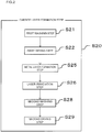
- a method for manufacturing a silicon carbide semiconductor device in the embodiment includes, as illustrated in Fig. 1 , a step for forming a front-surface electrode 30 including metal on a front surface side of a silicon carbide wafer 10 (front-surface electrode formation step S15, see Fig. 4(b) ), and a step for thinning the silicon carbide wafer 10 by reducing the thickness of the silicon carbide wafer 10 from a back surface side thereof (thinning step S16).
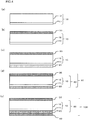
- the silicon carbide wafer 10 prepared in Fig. 4(a) includes, for example, a silicon carbide substrate 11 and a silicon carbide layer 12 formed on the silicon carbide substrate 11, for example, by epitaxial growth.
- the method for manufacturing the silicon carbide semiconductor device 100 includes a step for forming a carbide layer 20 (carbide layer formation step S20) .
- the carbide layer formation step S20 includes, as illustrated in Fig. 2 , a step for providing a metal layer 21 on the back surface of the thinned silicon carbide wafer 10 (metal layer formation step S25, see Fig.
- the entire metal layer 21 is changed into the carbide layer 20
- there is no limitation thereto only a part of the metal layer 21 on the back surface side thereof (a lower part of the metal layer 21 in Fig. 4(c) ) may be changed into the carbide layer 20, and a part of the metal layer 21 on the front surface side thereof (an upper part of the metal layer 21 in Fig. 4(c) ) may remain unchanged as the metal layer 21.
- by changing the entire metal layer 21 into the carbide layer 20 it is possible to more surely suppress warpage of the thinned silicon carbide wafer 10 (or a front-surface electrode-equipped silicon carbide base 51 described later) .
- the method for manufacturing the silicon carbide semiconductor device 100 includes a step for forming a back-surface electrode 40 including metal on a back surface side of the carbide layer 20 (back-surface electrode formation step S31, see Fig. 4(e) ).
- back-surface electrode formation step S31 see Fig. 4(e)
- a description will be given using, as an example, an aspect in which the front-surface electrode formation step S15, the thinning step S16, the metal layer formation step S25, the laser irradiation step S26, and the back-surface electrode formation step S31 are formed in order.
- the order of these steps can be appropriately changed.
- warpage of the silicon carbide wafer 10 generated in the thinning step S16 can be suppressed by performing the front-surface electrode formation step S15 prior to the thinning step S16, it is preferable to perform the front-surface electrode formation step S15 prior to the thinning step S16 from this viewpoint.
- the carbide layer formation step S20 includes a step for washing at least a back surface of the silicon carbide wafer 10 subjected to the thinning step S16 (first washing step S21), and a step for drying the silicon carbide wafer 10 subjected to the first washing step S21 (first drying step S22) .
- the carbide layer formation step S20 includes a step for washing a silicon carbide base 50 subjected to the laser irradiation step S26 and including the carbide layer 20 formed therein (second washing step S28), and a step for drying the silicon carbide wafer 10 subjected to the second washing step S28 (second drying step S29).
- the silicon carbide wafer 10 or the silicon carbide base 50 is rotated and dried (spin dry).
- the "silicon carbide base 50" means the silicon carbide wafer 10 including the carbide layer 20 formed on the back surface side thereof (see Fig. 3 ).
- the carbide layer 20, and the front-surface electrode 30 is indicated as the front-surface electrode-equipped silicon carbide base 51 (see Fig. 4(d) ).
- warpage is generated in the silicon carbide wafer 10 when the thickness of the silicon carbide wafer 10 is reduced by the thinning step S16.
- warpage of 100 ⁇ m or larger is generated on that occasion.
- the laser irradiation step S26 in the carbide layer formation step S20 may be performed, for example, under vacuum conditions and at a temperature of 1000°C.
- the method for manufacturing the silicon carbide semiconductor device 100 in the embodiment includes, as illustrated in Fig. 1 , a step for forming an alignment mark (alignment mark formation step S11), a step for forming a guard ring (guard ring formation step S12), a step for activating impurities (impurity activation step S13), and a step for forming a passivation film (passivation film formation step S14).
- these steps are performed prior to the front-surface electrode formation step S15 described above.
- the method for manufacturing the silicon carbide semiconductor device 100 in the embodiment includes, subsequent to the back-surface electrode formation step S31, a step for measuring electrical properties with a prober (prober measurement step S32), a step for dicing the silicon carbide base 50 (dicing step), and a step for mounting on a front surface of the silicon carbide base 50 (mounting step) .
- the dicing step and the mounting step are collectively illustrated as "S33".
- the metal layer 21 can be provided by deposition or sputtering.
- the thickness of the metal layer 21 to be provided is about 50 to 500 nm.
- laser light irradiation may be performed such that a portion to be irradiated with laser light partially overlaps with a portion which was irradiated with the laser light.
- a high-density portion 110 having high carbide density may be formed by overlapping of portions irradiated with the laser light
- a low-density portion 120 having low carbide density may be formed by non-overlapping of portions irradiated with the laser light.
- a low-density portion 121 having low carbide density may be formed by overlapping of portions irradiated with the laser light
- a high-density portion 111 having high carbide density may be formed by non-overlapping of portions irradiated with the laser light.
- Whether the high-density portion or the low-density portion is formed by overlapping of portions irradiated with laser light is determined depending on factors such as materials constituting the layer, intensity of laser light used for irradiation, an atmosphere in which the carbide layer 20 is formed (such as gas atmosphere, pressure, and temperature).
- laser light irradiation may be performed along a first direction in the carbide layer formation step S20.
- the first direction is a "vertical direction" in Fig. 6 .
- another laser light irradiation starting from another position spaced apart at a movement interval G, may be performed along the first direction.
- the expression "when a particular laser light irradiation is finished along the first direction” means, in a case where the laser light irradiation is performed from one end of a wafer along the first direction, when the laser light irradiation has been performed to the other end thereof.
- the "movement interval G" can be determined appropriately, and for example, may be an interval equivalent to 1/4 to 1/100 of a diameter of the wafer.
- the laser light irradiation for the position shifted by the movement interval G is finished from one end to the other end in a second direction perpendicular to the first direction (when a "first period” in Fig. 6 is finished)
- the laser light irradiation for a next period is performed.
- a portion for example, an intermediate position
- portions irradiated with the laser light in the previous period may be irradiated with the laser light (see Fig. 6 ), or the portions irradiated with the laser light in the previous period (the first period) may be irradiated with the laser light in an overlapping manner (see Fig. 7 ).
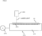
- the external force applied in the carbide layer formation step S20 may be applied by an adsorption power by a vacuum adsorption unit 270 illustrated in Fig. 5 .
- Absorption by the vacuum adsorption unit 270 may be set, for example, to 30 cmHg or more, and as an example, may be set to 30 cmHg or more and 60 cmcmHg or less.
- the vacuum adsorption unit 270 supports the front-surface electrode-equipped silicon carbide base 51, and includes a placement table 271 and a suction unit 272.
- the placement table 271 includes a plurality of suction holes 273 in a front surface thereof.
- the suction unit 272 includes a suction pump which applies, through the suction holes 273, a suction power to the silicon carbide wafer 10 placed on the placement table 271.
- the placement table 271 includes a hollow portion having a hollow shape in order to transmit the suction power from the suction unit 272 to the suction holes 273.
- the plurality of suction holes 273 may be successively provided in a line along the first direction, or may be successively provided in a line along the second direction perpendicular to the first direction. In addition, the plurality of suction holes 273 may not be provided in a line, but be placed on the surface of the placement table 271 concentrically at equal intervals. In a case where the plurality of suction holes 273 is successively provided in a line along the first direction, the plurality of suction holes 273 may be successively provided in parallel at intervals corresponding to the above-described "movement interval G", for example, intervals 0.5 to 2 times as long as the "movement interval G".
- the metal layer 21 formed in the metal layer formation step S25 may be a layer including titanium and molybdenum.
- the metal layer 21 may include only titanium, only molybdenum, or only titanium and molybdenum.
- the expression “only titanium” also means a case where a component other than titanium is included at an impurity level.
- the expression “only molybdenum” also means a case where a component other than molybdenum is included at an impurity level.
- the carbide layer 20 is formed by titanium carbide
- the carbide layer 20 is formed by molybdenum carbide.
- Green laser may be used as the laser light used in the carbide layer formation step S20.
- Output of the laser light may be set to 0.5 W or more at 10 kHZ, and for example, may be set to 0.5 W or more and 1.0 W or less.
- a total energy amount of laser may be set, for example, to 0.7 J/cm 2 or more, and for example, may be set to 0.7 J/cm 2 or more and 1.4 J/cm 2 or less.
- a laser scan speed may be set, for example, to 200 mm/sec or more, and for example, may be set to 200 mm/sec or more and 300 mm/sec or less.
- the silicon carbide semiconductor device 100 manufactured by the method for manufacturing the silicon carbide semiconductor device 100 according to the embodiment may include the silicon carbide wafer 10, the front-surface electrode 30 provided on the front surface side of the silicon carbide wafer 10, the carbide layer 20 provided on the back surface of the silicon carbide wafer 10 which has been thinned, and the back-surface electrode 40 provided on the back surface side of the carbide layer 20.
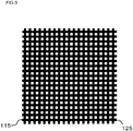
- the carbide layer 20 may include, as illustrated in Fig. 9 , a high-density portion 115 having high carbide density and a low-density portion 125 having low carbide density.
- the high-density portion 115 may be provided along two different directions which are in-plane directions of the carbide layer 20.
- An example of the two different directions includes, as illustrated in Fig. 9 , two directions which are perpendicular to each other in a plane of the silicon carbide wafer 10.
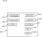
- a device used in the method for manufacturing the silicon carbide semiconductor device 100 according to the embodiment, as illustrated in the block diagram in Fig. 10 as an example, a device can be used which includes a first electrode formation unit 210, a thinning processing unit 230, a metal layer formation unit 250, an external force applying unit (in the embodiment, the vacuum adsorption unit 270), a laser light irradiation unit 260, and a second electrode formation unit 220.
- the first electrode formation unit 210 forms the front-surface electrode 30 on the front surface side of the silicon carbide wafer 10.
- the thinning processing unit 230 thins the silicon carbide wafer 10 by reducing the thickness of the silicon carbide wafer 10 from the back surface side thereof.
- the metal layer formation unit 250 provides the metal layer 21 on the back surface of the silicon carbide wafer 10 which has been thinned.
- the external force applying unit applies an external force such that the silicon carbide wafer 10 and the metal layer 21 are planarized.
- the laser light irradiation unit 260 irradiates the metal layer 21, to which the external force is being applied by the external force applying unit, with laser light to form the carbide layer 20 obtained by a reaction with carbon in the silicon carbide wafer, on the back surface side of the metal layer 21.
- the second electrode formation unit 220 forms the back-surface electrode 40 on the back surface side of the carbide layer 20.
- the external force is applied to the silicon carbide wafer 10.
- the manufacturing device 200 may include a drying unit 281 and a washing unit 282.
- the drying unit 281 performs the first drying step S22 and the second drying step S29 illustrated in Fig.2 .
- the washing unit 282 performs the first washing step S21 and the second washing step S28 illustrated in Fig.2 .
- first electrode formation unit 210 and the second electrode formation unit 220 those already known as a device for forming electrodes can be used.
- the first electrode formation unit 210 and the second electrode formation unit 220 may be devices different from each other, or may be devices the same as each other.
- a grinding device for grinding and reducing the thickness of the silicon carbide wafer 10 may be used, or a reactor for reducing the thickness of the silicon carbide wafer 10 with a chemical reaction may be used.
- a deposition device for depositing the metal layer 21 may be used, or a sputtering device for providing the metal layer 21 by performing sputtering may be used.
- the external force applying unit As the external force applying unit, the vacuum adsorption unit 270 described above, a pressing unit 290 used in a second embodiment, and the like can be used.
- the drying unit 281 for example, a spin dryer and the like can be used.
- the washing unit 282 a conventionally known wafer washing device can be used.
- the embodiment it is possible to eliminate or reduce warpage of the thinned silicon carbide wafer 10 by irradiating the metal layer 21 with laser light to form, not a silicide layer but the carbide layer 20, while applying an external force such that the silicon carbide wafer 10 and the metal layer 21 are planarized. Consequently, unlike the conventional technique provided by WO2012/049792 , it is possible to eliminate or reduce warpage of the thinned silicon carbide wafer 10 by a simple technique without removing an affected layer.
- the low-density portion and the high-density portion can be formed in a definite pattern in a plane of the silicon carbide wafer 10 (see Fig. 9 ).
- the carbide layer 20 can be surely formed on the silicon carbide wafer 10.
- a highly pure carbide layer 20 can be surely formed. As a result, it is possible to more surely eliminate or reduce warpage of the thinned silicon carbide wafer 10.
- the external force applied in the carbide layer formation step S20 has been applied by the adsorption power generated by the vacuum adsorption unit 270.
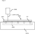
- the second embodiment adopts an aspect in which the external force applied in the carbide layer formation step S20 is applied by a pressing force by the pressing unit 290 made of a member which transmits laser light, as illustrated in Fig. 11 .
- a description will be given using an aspect in which the pressing unit 290 is used instead of the vacuum adsorption unit 270.
- the pressing unit 290 may be used together with the vacuum adsorption unit 270.
- the pressing unit 290 of the embodiment may be made of a material which transmits laser light.
- the pressing unit 290 may include a driving unit 292 and a pressing body 291.
- the driving unit 292 applies a pressing force.
- the pressing body 291 is connected to the driving unit 292 and transmits the pressing force from the driving unit to the silicon carbide wafer 10.
- the driving unit 292 may be connected to the placement table 275 or may be provided in the placement table 275.
- the pressing force may be applied to the silicon carbide wafer 10 by the driving unit 292 drawing the pressing body 291 toward the placement table 275.
- the driving unit 292 for example, those of hydraulic type can also be used.
- the pressing unit 290 is adopted as the external force applying unit, it is possible to physically planarize the silicon carbide wafer 10. Consequently, the carbide layer 20 can be formed while almost forcibly planarizing the silicon carbide wafer 10. As a result, it is possible to more surely eliminate or reduce warpage of the thinned silicon carbide wafer 10.
Landscapes
- Engineering & Computer Science (AREA)
- Physics & Mathematics (AREA)
- Microelectronics & Electronic Packaging (AREA)
- Power Engineering (AREA)
- Condensed Matter Physics & Semiconductors (AREA)
- General Physics & Mathematics (AREA)
- Computer Hardware Design (AREA)
- Manufacturing & Machinery (AREA)
- High Energy & Nuclear Physics (AREA)
- Ceramic Engineering (AREA)
- Crystallography & Structural Chemistry (AREA)
- Electromagnetism (AREA)
- Optics & Photonics (AREA)
- Chemical & Material Sciences (AREA)
- Health & Medical Sciences (AREA)
- Toxicology (AREA)
- Electrodes Of Semiconductors (AREA)
- Mechanical Treatment Of Semiconductor (AREA)
Abstract
Description
- The present invention relates to a method for manufacturing a silicon carbide semiconductor device, a method for manufacturing a semiconductor base, a silicon carbide semiconductor device, and a device for manufacturing a silicon carbide semiconductor device.
- Conventionally, reduction in thickness (thinning) of a silicon carbide wafer has been attempted in order to reduce a thickness of a silicon carbide element. When reducing a thickness of a silicon carbide wafer, for example, a grinding technique is used. On the other hand, when reducing a thickness of a silicon carbide wafer, warpage may be generated. As a technique for eliminating such warpage, for example, the following technique is proposed in
WO2012/049792 (paragraph [0038]). (1) After thinning is performed, a Ni film is formed on a back surface, and then laser annealing is performed to the Ni film, thereby forming a silicide layer. (2) By thinning a substrate (wafer) as described above, large warpage is generated. However, an amount of the warpage of the substrate (wafer) is adjusted by removing (surface-treating) at least a part of an affected layer formed on a ground surface after the thinning. - The present invention provides a method for manufacturing a silicon carbide semiconductor device, a method for manufacturing a semiconductor base, a silicon carbide semiconductor device, and a device for manufacturing a silicon carbide semiconductor device, with which warpage is eliminated or reduced in a thinned silicon carbide wafer by a simple technique without removing an affected layer, unlike conventional
WO2012/049792 . - A method for manufacturing a silicon carbide semiconductor device comprises:
- a step for forming a front-surface electrode on a front surface side of a silicon carbide wafer;
- a step for thinning the silicon carbide wafer by reducing a thickness of the silicon carbide wafer from a back surface side thereof;
- a step for providing a metal layer on the back surface of the thinned silicon carbide wafer;
- a step for irradiating the metal layer with laser light, while applying an external force such that the silicon carbide wafer and the metal layer are planarized, to form the carbide layer obtained by a reaction with carbon in the silicon carbide wafer, on a back surface side of the metal layer; and
- a step for forming a back-surface electrode on a back surface side of the carbide layer.
- In the method for manufacturing the silicon carbide semiconductor device according to the present invention,
the laser light irradiation may be performed such that a portion to be irradiated with laser light partially overlaps with a portion which was irradiated with the laser light,
a high-density portion having high carbide density may be formed by overlapping of portions irradiated with the laser light, and
wherein a low-density portion having low carbide density may be formed by non-overlapping of portions irradiated with the laser light. - In the method for manufacturing the silicon carbide semiconductor device according to the present invention,
the laser light irradiation may be performed such that a portion to be irradiated with laser light partially overlaps with a portion which was irradiated with the laser light,
a low-density portion having low carbide density may be formed by overlapping of portions irradiated with the laser light, and
a high-density portion having high carbide density may be formed by non-overlapping of portions irradiated with the laser light. - In the method for manufacturing the silicon carbide semiconductor device according to the present invention,
wherein the laser light irradiation is performed along a first direction,
wherein when a particular laser light irradiation is finished along the first direction, another laser light irradiation, starting from another position spaced apart at an interval, is performed along the first direction. - In the method for manufacturing the silicon carbide semiconductor device according to the present invention,
wherein the external force is applied by an adsorption power by a vacuum adsorption unit, or by a pressing force by a pressing unit made of a member which transmits the laser light. - In the method for manufacturing the silicon carbide semiconductor device according to the present invention,
wherein the metal layer is titanium, molybdenum, or titanium and molybdenum. - In the method for manufacturing the silicon carbide semiconductor device according to the present invention,
wherein the laser light is green laser. - A method for manufacturing a semiconductor base comprises:
- a step for thinning a silicon carbide wafer by reducing a thickness of the silicon carbide wafer from a back surface side thereof;
- a step for providing a metal layer on the back surface of the thinned silicon carbide wafer; and
- a step for irradiating the metal layer with laser light, while applying an external force such that the silicon carbide wafer and the metal layer are planarized, to form the carbide layer obtained by a reaction with carbon in the silicon carbide wafer, on a back surface side of the metal layer.
- A silicon carbide semiconductor device comprises:
- a silicon carbide wafer,
- a front-surface electrode provided on a front surface side of the silicon carbide wafer,
- a carbide layer provided on a back surface of the silicon carbide wafer which has been thinned, and
- a back-surface electrode provided on a back surface side of the carbide layer
- wherein the carbide layer includes a high-density portion having high carbide density and a low-density portion having low carbide density, and
- wherein the high-density portion is provided along two different directions which are in-plane directions of the carbide layer.
- A manufacturing device comprises:
- a first electrode formation unit, which forms a front-surface electrode on a front surface side of a silicon carbide wafer;
- a thinning processing unit, which thins the silicon carbide wafer by reducing the thickness of the silicon carbide wafer from the back surface side thereof;
- a metal layer formation unit, which provides a metal layer on a back surface of the silicon carbide wafer which has been thinned;
- an external force applying unit, which applies an external force such that the silicon carbide wafer and the metal layer are planarized;
- a laser light irradiation unit, which irradiates the metal layer, while the external force is being applied by the external force applying unit, with laser light to form a carbide layer obtained by a reaction with carbon in the silicon carbide wafer, on the back surface side of the metal layer; and
- a second electrode formation unit, which forms a back-surface electrode on a back surface side of the carbide layer.
- According to the present invention, it is possible to eliminate or reduce warpage of the thinned silicon carbide wafer by irradiating the metal layer with laser light to form, not a silicide layer but the carbide layer, while applying an external force such that the silicon carbide wafer and the metal layer are planarized. Consequently, unlike the conventional technique provided by
WO2012/049792 , it is possible to eliminate or reduce warpage of the thinned silicon carbide wafer by a simple technique without removing an affected layer. -
-
Fig. 1 illustrates steps in a method for manufacturing a silicon carbide semiconductor device according to a first embodiment of the present invention. -
Fig. 2 illustrates steps included in a carbide layer formation step according to the first embodiment of the present invention. -
Fig. 3 is a sectional view illustrating a layer configuration of the silicon carbide semiconductor device according to the first embodiment of the present invention. -
Figs. 4 (a) to 4 (e) are sectional views illustrating a layer configuration regarding a part of steps for manufacturing the silicon carbide semiconductor device according to the first embodiment of the present invention. -
Fig. 5 is a side view schematically illustrating a part of a manufacturing device for manufacturing the silicon carbide semiconductor device according to the first embodiment of the present invention. -
Fig. 6 is a plan view illustrating an aspect in which irradiation with laser light is performed in a laser irradiation step according to the first embodiment of the present invention. -
Fig. 7 is a plan view illustrating an aspect in which the laser light partially overlaps in the laser irradiation step according to the first embodiment of the present invention. -
Fig. 8(a) is a plan view illustrating an aspect in which a portion irradiated with the laser light in an overlapping manner has become a high-density portion, and a portion irradiated with the laser light in a non-overlapping manner has become a low-density portion in a carbide layer formed in the first embodiment of the present invention.Fig. 8 (b) is a plan view illustrating an aspect in which a portion irradiated with the laser light in an overlapping manner has become a low-density portion, and a portion irradiated with the laser light in a non-overlapping manner has become a high-density portion in the carbide layer formed in the first embodiment of the present invention. -
Fig. 9 is a plan view illustrating an aspect in which the high-density portion is formed into a lattice shape in the carbide layer formed in the first embodiment of the present invention. -
Fig. 10 is a block diagram illustrating a part of the manufacturing device for manufacturing the silicon carbide semiconductor device according to the first embodiment of the present invention. -
Fig. 11 is a side view schematically illustrating a part of a manufacturing device for manufacturing a silicon carbide semiconductor device according to a second embodiment of the present invention. - A method for manufacturing a silicon carbide semiconductor device in the embodiment includes, as illustrated in
Fig. 1 , a step for forming a front-surface electrode 30 including metal on a front surface side of a silicon carbide wafer 10 (front-surface electrode formation step S15, seeFig. 4(b) ), and a step for thinning thesilicon carbide wafer 10 by reducing the thickness of thesilicon carbide wafer 10 from a back surface side thereof (thinning step S16). Thesilicon carbide wafer 10 prepared inFig. 4(a) includes, for example, asilicon carbide substrate 11 and asilicon carbide layer 12 formed on thesilicon carbide substrate 11, for example, by epitaxial growth. - As illustrated in
Fig. 1 , the method for manufacturing the siliconcarbide semiconductor device 100 includes a step for forming a carbide layer 20 (carbide layer formation step S20) . The carbide layer formation step S20 includes, as illustrated inFig. 2 , a step for providing ametal layer 21 on the back surface of the thinned silicon carbide wafer 10 (metal layer formation step S25, seeFig. 4(c) ), and a step for irradiating themetal layer 21 with laser light, while applying an external force such that thesilicon carbide wafer 10 and themetal layer 21 are planarized, to form thecarbide layer 20 obtained by a reaction with carbon in the silicon carbide wafer, on a back surface side of the metal layer 21 (laser irradiation step S26, seeFig. 4(d) ). - In the embodiment, although a description will be given using an aspect in which the
entire metal layer 21 is changed into thecarbide layer 20, there is no limitation thereto. For example, only a part of themetal layer 21 on the back surface side thereof (a lower part of themetal layer 21 inFig. 4(c) ) may be changed into thecarbide layer 20, and a part of themetal layer 21 on the front surface side thereof (an upper part of themetal layer 21 inFig. 4(c) ) may remain unchanged as themetal layer 21. However, by changing theentire metal layer 21 into thecarbide layer 20, it is possible to more surely suppress warpage of the thinned silicon carbide wafer 10 (or a front-surface electrode-equippedsilicon carbide base 51 described later) . In addition, from the viewpoint of obtaining an effect of more surely suppressing warpage, it is more preferable to change the entire surface of themetal layer 21 into thecarbide layer 20 than to change a part thereof into thecarbide layer 20 in an in-plane direction. - As illustrated in
Fig. 1 , the method for manufacturing the siliconcarbide semiconductor device 100 includes a step for forming a back-surface electrode 40 including metal on a back surface side of the carbide layer 20 (back-surface electrode formation step S31, seeFig. 4(e) ). In the embodiment, a description will be given using, as an example, an aspect in which the front-surface electrode formation step S15, the thinning step S16, the metal layer formation step S25, the laser irradiation step S26, and the back-surface electrode formation step S31 are formed in order. However, there is no limitation thereto, and the order of these steps can be appropriately changed. However, since warpage of thesilicon carbide wafer 10 generated in the thinning step S16 can be suppressed by performing the front-surface electrode formation step S15 prior to the thinning step S16, it is preferable to perform the front-surface electrode formation step S15 prior to the thinning step S16 from this viewpoint. - As illustrated in
Fig. 2 , the carbide layer formation step S20 includes a step for washing at least a back surface of thesilicon carbide wafer 10 subjected to the thinning step S16 (first washing step S21), and a step for drying thesilicon carbide wafer 10 subjected to the first washing step S21 (first drying step S22) . In addition, the carbide layer formation step S20 includes a step for washing asilicon carbide base 50 subjected to the laser irradiation step S26 and including thecarbide layer 20 formed therein (second washing step S28), and a step for drying thesilicon carbide wafer 10 subjected to the second washing step S28 (second drying step S29). Regarding the first drying step S22 and the second drying step S29, an aspect may be adopted in which thesilicon carbide wafer 10 or thesilicon carbide base 50 is rotated and dried (spin dry). In the embodiment, the "silicon carbide base 50" means thesilicon carbide wafer 10 including thecarbide layer 20 formed on the back surface side thereof (seeFig. 3 ). In the embodiment, that which includes thesilicon carbide wafer 10, thecarbide layer 20, and the front-surface electrode 30 is indicated as the front-surface electrode-equipped silicon carbide base 51 (seeFig. 4(d) ). - In general, warpage is generated in the
silicon carbide wafer 10 when the thickness of thesilicon carbide wafer 10 is reduced by the thinning step S16. As an example, warpage of 100 µm or larger is generated on that occasion. In addition, the laser irradiation step S26 in the carbide layer formation step S20 may be performed, for example, under vacuum conditions and at a temperature of 1000°C. - Besides, the method for manufacturing the silicon
carbide semiconductor device 100 in the embodiment includes, as illustrated inFig. 1 , a step for forming an alignment mark (alignment mark formation step S11), a step for forming a guard ring (guard ring formation step S12), a step for activating impurities (impurity activation step S13), and a step for forming a passivation film (passivation film formation step S14). As an example, these steps are performed prior to the front-surface electrode formation step S15 described above. In addition, the method for manufacturing the siliconcarbide semiconductor device 100 in the embodiment includes, subsequent to the back-surface electrode formation step S31, a step for measuring electrical properties with a prober (prober measurement step S32), a step for dicing the silicon carbide base 50 (dicing step), and a step for mounting on a front surface of the silicon carbide base 50 (mounting step) . InFig. 1 , the dicing step and the mounting step are collectively illustrated as "S33". - Various methods can be adopted to provide the
metal layer 21. For example, themetal layer 21 can be provided by deposition or sputtering. As an example, the thickness of themetal layer 21 to be provided is about 50 to 500 nm. - In the carbide layer formation step S20, as illustrated in
Fig. 7 , laser light irradiation may be performed such that a portion to be irradiated with laser light partially overlaps with a portion which was irradiated with the laser light. Then, as illustrated inFig. 8 (a) , a high-density portion 110 having high carbide density may be formed by overlapping of portions irradiated with the laser light, and a low-density portion 120 having low carbide density may be formed by non-overlapping of portions irradiated with the laser light. To the contrary, as illustrated inFig. 8 (b) , a low-density portion 121 having low carbide density may be formed by overlapping of portions irradiated with the laser light, and a high-density portion 111 having high carbide density may be formed by non-overlapping of portions irradiated with the laser light. Whether the high-density portion or the low-density portion is formed by overlapping of portions irradiated with laser light is determined depending on factors such as materials constituting the layer, intensity of laser light used for irradiation, an atmosphere in which thecarbide layer 20 is formed (such as gas atmosphere, pressure, and temperature). - As illustrated in
Fig. 6 , laser light irradiation may be performed along a first direction in the carbide layer formation step S20. The first direction is a "vertical direction" inFig. 6 . When a particular laser light irradiation is finished along the first direction, another laser light irradiation, starting from another position spaced apart at a movement interval G, may be performed along the first direction. The expression "when a particular laser light irradiation is finished along the first direction" means, in a case where the laser light irradiation is performed from one end of a wafer along the first direction, when the laser light irradiation has been performed to the other end thereof. The "movement interval G" can be determined appropriately, and for example, may be an interval equivalent to 1/4 to 1/100 of a diameter of the wafer. - When the laser light irradiation for the position shifted by the movement interval G is finished from one end to the other end in a second direction perpendicular to the first direction (when a "first period" in
Fig. 6 is finished), the laser light irradiation for a next period (a "second period" inFig. 6 ) is performed. On that occasion, a portion (for example, an intermediate position) between portions irradiated with the laser light in the previous period (the first period) may be irradiated with the laser light (seeFig. 6 ), or the portions irradiated with the laser light in the previous period (the first period) may be irradiated with the laser light in an overlapping manner (seeFig. 7 ). - The external force applied in the carbide layer formation step S20 may be applied by an adsorption power by a
vacuum adsorption unit 270 illustrated inFig. 5 . Absorption by thevacuum adsorption unit 270 may be set, for example, to 30 cmHg or more, and as an example, may be set to 30 cmHg or more and 60 cmcmHg or less. - As illustrated in
Fig. 5 , thevacuum adsorption unit 270 supports the front-surface electrode-equippedsilicon carbide base 51, and includes a placement table 271 and asuction unit 272. The placement table 271 includes a plurality of suction holes 273 in a front surface thereof. Thesuction unit 272 includes a suction pump which applies, through the suction holes 273, a suction power to thesilicon carbide wafer 10 placed on the placement table 271. Although it is not illustrated inFig. 5 , the placement table 271 includes a hollow portion having a hollow shape in order to transmit the suction power from thesuction unit 272 to the suction holes 273. The plurality of suction holes 273 may be successively provided in a line along the first direction, or may be successively provided in a line along the second direction perpendicular to the first direction. In addition, the plurality of suction holes 273 may not be provided in a line, but be placed on the surface of the placement table 271 concentrically at equal intervals. In a case where the plurality of suction holes 273 is successively provided in a line along the first direction, the plurality of suction holes 273 may be successively provided in parallel at intervals corresponding to the above-described "movement interval G", for example, intervals 0.5 to 2 times as long as the "movement interval G". - The
metal layer 21 formed in the metal layer formation step S25 may be a layer including titanium and molybdenum. Themetal layer 21 may include only titanium, only molybdenum, or only titanium and molybdenum. The expression "only titanium" also means a case where a component other than titanium is included at an impurity level. Likewise, the expression "only molybdenum" also means a case where a component other than molybdenum is included at an impurity level. When only titanium is used as themetal layer 21, thecarbide layer 20 is formed by titanium carbide, and when only molybdenum is used as themetal layer 21, thecarbide layer 20 is formed by molybdenum carbide. - Green laser may be used as the laser light used in the carbide layer formation step S20. Output of the laser light may be set to 0.5 W or more at 10 kHZ, and for example, may be set to 0.5 W or more and 1.0 W or less. A total energy amount of laser may be set, for example, to 0.7 J/cm2 or more, and for example, may be set to 0.7 J/cm2 or more and 1.4 J/cm2 or less. A laser scan speed may be set, for example, to 200 mm/sec or more, and for example, may be set to 200 mm/sec or more and 300 mm/sec or less.
- As illustrated in
Fig. 3 , the siliconcarbide semiconductor device 100 manufactured by the method for manufacturing the siliconcarbide semiconductor device 100 according to the embodiment may include thesilicon carbide wafer 10, the front-surface electrode 30 provided on the front surface side of thesilicon carbide wafer 10, thecarbide layer 20 provided on the back surface of thesilicon carbide wafer 10 which has been thinned, and the back-surface electrode 40 provided on the back surface side of thecarbide layer 20. Thecarbide layer 20 may include, as illustrated inFig. 9 , a high-density portion 115 having high carbide density and a low-density portion 125 having low carbide density. In addition, the high-density portion 115 may be provided along two different directions which are in-plane directions of thecarbide layer 20. An example of the two different directions includes, as illustrated inFig. 9 , two directions which are perpendicular to each other in a plane of thesilicon carbide wafer 10. With the high-density portion 115 thus formed into a lattice shape, it is possible to more surely suppress warpage of the thinned silicon carbide wafer 10 (or the front-surface electrode-equipped silicon carbide base 51). - As a
manufacturing device 200 used in the method for manufacturing the siliconcarbide semiconductor device 100 according to the embodiment, as illustrated in the block diagram inFig. 10 as an example, a device can be used which includes a firstelectrode formation unit 210, a thinningprocessing unit 230, a metallayer formation unit 250, an external force applying unit (in the embodiment, the vacuum adsorption unit 270), a laserlight irradiation unit 260, and a secondelectrode formation unit 220. The firstelectrode formation unit 210 forms the front-surface electrode 30 on the front surface side of thesilicon carbide wafer 10. The thinningprocessing unit 230 thins thesilicon carbide wafer 10 by reducing the thickness of thesilicon carbide wafer 10 from the back surface side thereof. The metallayer formation unit 250 provides themetal layer 21 on the back surface of thesilicon carbide wafer 10 which has been thinned. The external force applying unit applies an external force such that thesilicon carbide wafer 10 and themetal layer 21 are planarized. The laserlight irradiation unit 260 irradiates themetal layer 21, to which the external force is being applied by the external force applying unit, with laser light to form thecarbide layer 20 obtained by a reaction with carbon in the silicon carbide wafer, on the back surface side of themetal layer 21. The secondelectrode formation unit 220 forms the back-surface electrode 40 on the back surface side of thecarbide layer 20. In the embodiment, by applying an external force to the front-surface electrode-equippedsilicon carbide base 51 by the external force applying unit, the external force is applied to thesilicon carbide wafer 10. - As illustrated in the block diagram in
Fig. 10 , themanufacturing device 200 may include adrying unit 281 and awashing unit 282. The dryingunit 281 performs the first drying step S22 and the second drying step S29 illustrated inFig.2 . Thewashing unit 282 performs the first washing step S21 and the second washing step S28 illustrated inFig.2 . - As the first
electrode formation unit 210 and the secondelectrode formation unit 220, those already known as a device for forming electrodes can be used. The firstelectrode formation unit 210 and the secondelectrode formation unit 220 may be devices different from each other, or may be devices the same as each other. - As the thinning
processing unit 230, for example, a grinding device for grinding and reducing the thickness of thesilicon carbide wafer 10 may be used, or a reactor for reducing the thickness of thesilicon carbide wafer 10 with a chemical reaction may be used. - As the metal
layer formation unit 250, for example, a deposition device for depositing themetal layer 21 may be used, or a sputtering device for providing themetal layer 21 by performing sputtering may be used. - As the external force applying unit, the
vacuum adsorption unit 270 described above, apressing unit 290 used in a second embodiment, and the like can be used. As thedrying unit 281, for example, a spin dryer and the like can be used. As thewashing unit 282, a conventionally known wafer washing device can be used. - Next, an operation and an effect exhibited by the embodiment including the above-described configuration will be described.
- According to the embodiment, it is possible to eliminate or reduce warpage of the thinned
silicon carbide wafer 10 by irradiating themetal layer 21 with laser light to form, not a silicide layer but thecarbide layer 20, while applying an external force such that thesilicon carbide wafer 10 and themetal layer 21 are planarized. Consequently, unlike the conventional technique provided byWO2012/049792 , it is possible to eliminate or reduce warpage of the thinnedsilicon carbide wafer 10 by a simple technique without removing an affected layer. - In the embodiment, in a case where an aspect is adopted in which laser light irradiation is performed such that a portion to be irradiated with laser light partially overlaps with a portion which was irradiated with the laser light, as illustrated in
Fig. 8 (a) , it is possible to form a high-density portion having high carbide density by overlapping of portions irradiated with the laser light, and to form a low-density portion having low carbide density by non-overlapping of portions irradiated with the laser light. Alternatively, as illustrated inFig. 8(b) , it is possible to form a low-density portion having low carbide density by overlapping of portions irradiated with the laser light, and to forma a high-density portion having high carbide density by non-overlapping of portions irradiated with the laser light. As a result, the low-density portion and the high-density portion can be formed in a definite pattern in a plane of the silicon carbide wafer 10 (seeFig. 9 ). By the aspect as described above, it is possible to more surely eliminate or reduce warpage of the thinnedsilicon carbide wafer 10. - In the embodiment, in a case where an aspect is adopted in which when a particular laser light irradiation is finished along the first direction, another laser light irradiation, starting from another position spaced apart at a movement interval G, is performed along the first direction, as illustrated in
Fig. 6 , it is possible to reduce an influence of fluctuation of intensity of laser light, and to make thecarbide layer 20 more uniform. There may be a case where laser light irradiation cannot be always performed at a constant intensity. Even in such a case, when the aspect is adopted, it is possible to reduce an influence of fluctuation of intensity of the laser light. As a result, it is possible to make properties (such as thickness and density) of thecarbide layer 20 formed on thesilicon carbide wafer 10 more uniform, and therefore, to more surely eliminate or reduce warpage of the thinnedsilicon carbide wafer 10. - In a case where the
vacuum adsorption unit 270 is adopted as the external force applying unit as illustrated inFig. 5 , an external force can be applied uniformly. In addition, since other member is not positioned in a portion irradiated with the laser light, there is no influence of the "other member". Therefore, it is possible to form thecarbide layer 20 while applying the external force, which is a uniform force, and making the intensity of the laser light and the like uniform. Accordingly, it is possible to more surely eliminate or reduce warpage of the thinnedsilicon carbide wafer 10. - By using titanium and/or molybdenum as the
metal layer 21, thecarbide layer 20 can be surely formed on thesilicon carbide wafer 10. When using only titanium, only molybdenum, or only titanium and molybdenum as a material of themetal layer 21, a highlypure carbide layer 20 can be surely formed. As a result, it is possible to more surely eliminate or reduce warpage of the thinnedsilicon carbide wafer 10. - When green laser is used as the laser light, an inexpensive device can be adopted as the laser light irradiation unit 260 (see
Fig. 5 ). Therefore, it is possible to manufacture products without spending much introduction cost or much maintenance cost. - Next, a second embodiment of the present invention will be described.
- In the first embodiment, the external force applied in the carbide layer formation step S20 has been applied by the adsorption power generated by the
vacuum adsorption unit 270. On the other hand, the second embodiment adopts an aspect in which the external force applied in the carbide layer formation step S20 is applied by a pressing force by thepressing unit 290 made of a member which transmits laser light, as illustrated inFig. 11 . In the embodiment, a description will be given using an aspect in which thepressing unit 290 is used instead of thevacuum adsorption unit 270. However, there is no limitation thereto, and thepressing unit 290 may be used together with thevacuum adsorption unit 270. - The
pressing unit 290 of the embodiment may be made of a material which transmits laser light. Regarding thepressing unit 290, an aspect may be adopted in which thesilicon carbide wafer 10 is pressed nearly entirely, or an aspect may be adopted in which only a part of thesilicon carbide wafer 10, for example, only four end portions and a central portion are pressed. Thepressing unit 290 may include adriving unit 292 and apressing body 291. The drivingunit 292 applies a pressing force. Thepressing body 291 is connected to thedriving unit 292 and transmits the pressing force from the driving unit to thesilicon carbide wafer 10. As illustrated inFig. 11 , the drivingunit 292 may be connected to the placement table 275 or may be provided in the placement table 275. The pressing force may be applied to thesilicon carbide wafer 10 by the drivingunit 292 drawing thepressing body 291 toward the placement table 275. As thedriving unit 292, for example, those of hydraulic type can also be used. - Other configuration in the second embodiment adopts substantially the same aspect as that of the first embodiment.
- The same effect as that of the first embodiment can be obtained with the embodiment. In addition, since the
pressing unit 290 is adopted as the external force applying unit, it is possible to physically planarize thesilicon carbide wafer 10. Consequently, thecarbide layer 20 can be formed while almost forcibly planarizing thesilicon carbide wafer 10. As a result, it is possible to more surely eliminate or reduce warpage of the thinnedsilicon carbide wafer 10. - Lastly, descriptions on the aforementioned respective embodiments and variations as well as disclosed drawings are merely examples for describing the invention described in CLAIMS. The descriptions on the aforementioned embodiments or disclosed drawings should not be construed to limit the invention described in CLAIMS.
-
- 10 Silicon carbide wafer
- 20 Carbide layer
- 21 Metal layer
- 30 Front-surface electrode
- 40 Back-surface electrode
- 100 Silicon carbide semiconductor device
- 110, 111, 115 High-density portion
- 120, 121, 125 Low-density portion
- 200 Manufacturing device for a silicon carbide semiconductor device
- 210 First electrode formation unit
- 220 Second electrode formation unit
- 230 Thinning processing unit
- 250 Metal layer formation unit
- 260 Laser light irradiation unit
- 270 Vacuum adsorption unit
- 290 Pressing unit
Claims (10)
- A method for manufacturing a silicon carbide semiconductor device comprising:a step for forming a front-surface electrode on a front surface side of a silicon carbide wafer;a step for thinning the silicon carbide wafer by reducing a thickness of the silicon carbide wafer from a back surface side thereof;a step for providing a metal layer on the back surface of the thinned silicon carbide wafer;a step for irradiating the metal layer with laser light, while applying an external force such that the silicon carbide wafer and the metal layer are planarized, to form the carbide layer obtained by a reaction with carbon in the silicon carbide wafer, on a back surface side of the metal layer; anda step for forming a back-surface electrode on a back surface side of the carbide layer.
- The method for manufacturing the silicon carbide semiconductor device according to claim 1,
wherein the laser light irradiation is performed such that a portion to be irradiated with laser light partially overlaps with a portion which was irradiated with the laser light,
wherein a high-density portion having high carbide density is formed by overlapping of portions irradiated with the laser light, and
wherein a low-density portion having low carbide density is formed by non-overlapping of portions irradiated with the laser light. - The method for manufacturing the silicon carbide semiconductor device according to claim 1,
wherein the laser light irradiation is performed such that a portion to be irradiated with laser light partially overlaps with a portion which was irradiated with the laser light,
wherein a low-density portion having low carbide density is formed by overlapping of portions irradiated with the laser light, and
wherein a high-density portion having high carbide density is formed by non-overlapping of portions irradiated with the laser light. - The method for manufacturing the silicon carbide semiconductor device according to any one of claims 1 to 3,
wherein the laser light irradiation is performed along a first direction,
wherein when a particular laser light irradiation is finished along the first direction, another laser light irradiation, starting from another position spaced apart at an interval, is performed along the first direction. - The method for manufacturing the silicon carbide semiconductor device according to any one of claims 1 to 4,
wherein the external force is applied by an adsorption power by a vacuum adsorption unit, or by a pressing force by a pressing unit made of a member which transmits the laser light. - The method for manufacturing the silicon carbide semiconductor device according to any one of claims 1 to 5,
wherein the metal layer is titanium, molybdenum, or titanium and molybdenum. - The method for manufacturing the silicon carbide semiconductor device according to any one of claims 1 to 6,
wherein the laser light is green laser. - A method for manufacturing a semiconductor base comprising:a step for thinning a silicon carbide wafer by reducing a thickness of the silicon carbide wafer from a back surface side thereof;a step for providing a metal layer on the back surface of the thinned silicon carbide wafer; anda step for irradiating the metal layer with laser light, while applying an external force such that the silicon carbide wafer and the metal layer are planarized, to form the carbide layer obtained by a reaction with carbon in the silicon carbide wafer, on a back surface side of the metal layer.
- A silicon carbide semiconductor device comprising:a silicon carbide wafer,a front-surface electrode provided on a front surface side of the silicon carbide wafer,a carbide layer provided on a back surface of the silicon carbide wafer which has been thinned, anda back-surface electrode provided on a back surface side of the carbide layerwherein the carbide layer includes a high-density portion having high carbide density and a low-density portion having low carbide density, andwherein the high-density portion is provided along two different directions which are in-plane directions of the carbide layer.
- A manufacturing device comprising:a first electrode formation unit, which forms a front-surface electrode on a front surface side of a silicon carbide wafer;a thinning processing unit, which thins the silicon carbide wafer by reducing the thickness of the silicon carbide wafer from the back surface side thereof;a metal layer formation unit, which provides a metal layer on a back surface of the silicon carbide wafer which has been thinned;an external force applying unit, which applies an external force such that the silicon carbide wafer and the metal layer are planarized;a laser light irradiation unit, which irradiates the metal layer, while the external force is being applied by the external force applying unit, with laser light to form a carbide layer obtained by a reaction with carbon in the silicon carbide wafer, on the back surface side of the metal layer; anda second electrode formation unit, which forms a back-surface electrode on a back surface side of the carbide layer.
Applications Claiming Priority (1)
| Application Number | Priority Date | Filing Date | Title |
|---|---|---|---|
| PCT/JP2015/084828 WO2017098659A1 (en) | 2015-12-11 | 2015-12-11 | Method for manufacturing silicon carbide semiconductor device, method for manufacturing semiconductor base body, silicon carbide semiconductor device, and apparatus for manufacturing silicon carbide semiconductor device |
Publications (3)
| Publication Number | Publication Date |
|---|---|
| EP3389082A1 true EP3389082A1 (en) | 2018-10-17 |
| EP3389082A4 EP3389082A4 (en) | 2019-08-07 |
| EP3389082B1 EP3389082B1 (en) | 2020-10-28 |
Family
ID=57981556
Family Applications (1)
| Application Number | Title | Priority Date | Filing Date |
|---|---|---|---|
| EP15884168.4A Active EP3389082B1 (en) | 2015-12-11 | 2015-12-11 | Method for manufacturing silicon carbide semiconductor device |
Country Status (6)
| Country | Link |
|---|---|
| US (1) | US9911811B2 (en) |
| EP (1) | EP3389082B1 (en) |
| JP (1) | JP6076548B1 (en) |
| CN (1) | CN107533961B (en) |
| TW (1) | TWI629715B (en) |
| WO (1) | WO2017098659A1 (en) |
Families Citing this family (5)
| Publication number | Priority date | Publication date | Assignee | Title |
|---|---|---|---|---|
| CN109791880A (en) * | 2016-10-13 | 2019-05-21 | 三菱电机株式会社 | The manufacturing method of semiconductor device |
| CN107649785A (en) * | 2017-09-22 | 2018-02-02 | 北京世纪金光半导体有限公司 | A kind of wafer thining method and device |
| DE112019001691T5 (en) * | 2018-03-30 | 2020-12-17 | Rohm Co., Ltd. | SEMI-CONDUCTOR COMPONENT |
| JP7487739B2 (en) | 2019-07-17 | 2024-05-21 | 住友電気工業株式会社 | Semiconductor chip and method for manufacturing the same |
| CN113097069A (en) * | 2021-03-31 | 2021-07-09 | 中国科学院微电子研究所 | Method for manufacturing semiconductor device |
Family Cites Families (13)
| Publication number | Priority date | Publication date | Assignee | Title |
|---|---|---|---|---|
| US7732301B1 (en) * | 2007-04-20 | 2010-06-08 | Pinnington Thomas Henry | Bonded intermediate substrate and method of making same |
| JP5369762B2 (en) | 2009-03-02 | 2013-12-18 | 株式会社デンソー | Method for manufacturing silicon carbide semiconductor device |
| JP5448652B2 (en) * | 2009-09-01 | 2014-03-19 | 三菱電機株式会社 | Semiconductor device and manufacturing method thereof |
| WO2012049792A1 (en) | 2010-10-15 | 2012-04-19 | 三菱電機株式会社 | Method for producing silicon carbide semiconductor device |
| CN103229275B (en) * | 2011-04-11 | 2015-10-07 | 新电元工业株式会社 | Manufacturing silicon carbide semiconductor device and manufacture method thereof |
| JP5877005B2 (en) | 2011-07-29 | 2016-03-02 | 株式会社Screenホールディングス | Substrate processing apparatus, substrate holding apparatus, and substrate holding method |
| WO2013051555A1 (en) * | 2011-10-07 | 2013-04-11 | 旭硝子株式会社 | Single-crystal silicon-carbide substrate and polishing solution |
| JP5886005B2 (en) * | 2011-11-14 | 2016-03-16 | ルネサスエレクトロニクス株式会社 | Manufacturing method of semiconductor device |
| WO2014065018A1 (en) * | 2012-10-23 | 2014-05-01 | 富士電機株式会社 | Semiconductor device manufacturing method |
| JP6197461B2 (en) * | 2013-08-06 | 2017-09-20 | 住友電気工業株式会社 | Silicon carbide semiconductor substrate, method of manufacturing the same, and method of manufacturing silicon carbide semiconductor device |
| JP6091406B2 (en) * | 2013-12-16 | 2017-03-08 | 三菱電機株式会社 | Method for manufacturing silicon carbide semiconductor device and laser annealing apparatus |
| WO2015163863A1 (en) * | 2014-04-23 | 2015-10-29 | United Silicon Carbide, Inc. | Formation of ohmic contacts on wide band gap semiconductors |
| JP6415946B2 (en) * | 2014-11-26 | 2018-10-31 | 株式会社東芝 | Semiconductor device manufacturing method and semiconductor device |
-
2015
- 2015-12-11 JP JP2016537032A patent/JP6076548B1/en active Active
- 2015-12-11 US US15/121,002 patent/US9911811B2/en active Active
- 2015-12-11 EP EP15884168.4A patent/EP3389082B1/en active Active
- 2015-12-11 CN CN201580007858.3A patent/CN107533961B/en active Active
- 2015-12-11 WO PCT/JP2015/084828 patent/WO2017098659A1/en active Application Filing
-
2016
- 2016-08-17 TW TW105126280A patent/TWI629715B/en active
Also Published As
| Publication number | Publication date |
|---|---|
| WO2017098659A1 (en) | 2017-06-15 |
| EP3389082A4 (en) | 2019-08-07 |
| CN107533961A (en) | 2018-01-02 |
| US9911811B2 (en) | 2018-03-06 |
| TW201721725A (en) | 2017-06-16 |
| JPWO2017098659A1 (en) | 2017-12-07 |
| EP3389082B1 (en) | 2020-10-28 |
| US20180019307A1 (en) | 2018-01-18 |
| TWI629715B (en) | 2018-07-11 |
| CN107533961B (en) | 2020-08-21 |
| JP6076548B1 (en) | 2017-02-08 |
Similar Documents
| Publication | Publication Date | Title |
|---|---|---|
| EP3389082B1 (en) | Method for manufacturing silicon carbide semiconductor device | |
| US10770350B2 (en) | Method of separating a back layer on a singulated semiconductor wafer attached to carrier substrate | |
| US8048775B2 (en) | Process of forming ultra thin wafers having an edge support ring | |
| US8664089B1 (en) | Semiconductor die singulation method | |
| WO2016112773A1 (en) | Three-dimensional electrode structure of semiconductor device, manufacturing method and application thereof | |
| US9034733B2 (en) | Semiconductor die singulation method | |
| US11075070B2 (en) | Monocrystalline semiconductor wafer and method for producing a semiconductor wafer | |
| TW201234459A (en) | Semiconductor manufacturing apparatus and semiconductor substrate bonding method | |
| PH12016000085B1 (en) | Semiconductor die back layer separation method | |
| WO2016113924A1 (en) | Semiconductor laminate | |
| CN105895488B (en) | The manufacturing method of plasma processing apparatus and electronic component | |
| JPWO2020136624A5 (en) | ||
| CN110318019A (en) | The manufacturing method of mask, mask support buffer substrate and its manufacturing method | |
| CN107154369A (en) | Method of plasma processing | |
| JP2008544945A (en) | Oxygen-sensitive silicon layer and method for obtaining the silicon layer | |
| CN110034018A (en) | The manufacturing method of semiconductor wafer | |
| CN113752401B (en) | Method for improving flatness of SiC wafer | |
| JP2008053595A (en) | Semiconductor wafer, and its manufacturing method | |
| JP6500792B2 (en) | Method of evaluating quality of epitaxial wafer and method of manufacturing the same | |
| RU2258978C2 (en) | Method for producing semiconductor structures | |
| KR20110080336A (en) | Apparatus for processing substrate have chuck pin | |
| US20140151854A1 (en) | Method for Separating a Layer and a Chip Formed on a Layer | |
| JP2013105924A (en) | Manufacturing method of silicon epitaxial wafer | |
| KR20130072014A (en) | Epitaxial wafer and method for preparing pattern |
Legal Events
| Date | Code | Title | Description |
|---|---|---|---|
| STAA | Information on the status of an ep patent application or granted ep patent |
Free format text: STATUS: THE INTERNATIONAL PUBLICATION HAS BEEN MADE |
|
| PUAI | Public reference made under article 153(3) epc to a published international application that has entered the european phase |
Free format text: ORIGINAL CODE: 0009012 |
|
| STAA | Information on the status of an ep patent application or granted ep patent |
Free format text: STATUS: REQUEST FOR EXAMINATION WAS MADE |
|
| 17P | Request for examination filed |
Effective date: 20180607 |
|
| AK | Designated contracting states |
Kind code of ref document: A1 Designated state(s): AL AT BE BG CH CY CZ DE DK EE ES FI FR GB GR HR HU IE IS IT LI LT LU LV MC MK MT NL NO PL PT RO RS SE SI SK SM TR |
|
| AX | Request for extension of the european patent |
Extension state: BA ME |
|
| DAV | Request for validation of the european patent (deleted) | ||
| DAX | Request for extension of the european patent (deleted) | ||
| A4 | Supplementary search report drawn up and despatched |
Effective date: 20190705 |
|
| RIC1 | Information provided on ipc code assigned before grant |
Ipc: H01L 21/268 20060101ALN20190701BHEP Ipc: H01L 21/28 20060101AFI20190701BHEP |
|
| GRAP | Despatch of communication of intention to grant a patent |
Free format text: ORIGINAL CODE: EPIDOSNIGR1 |
|
| STAA | Information on the status of an ep patent application or granted ep patent |
Free format text: STATUS: GRANT OF PATENT IS INTENDED |
|
| RIC1 | Information provided on ipc code assigned before grant |
Ipc: H01L 21/28 20060101AFI20200526BHEP Ipc: H01L 21/268 20060101ALN20200526BHEP |
|
| INTG | Intention to grant announced |
Effective date: 20200618 |
|
| GRAS | Grant fee paid |
Free format text: ORIGINAL CODE: EPIDOSNIGR3 |
|
| GRAA | (expected) grant |
Free format text: ORIGINAL CODE: 0009210 |
|
| STAA | Information on the status of an ep patent application or granted ep patent |
Free format text: STATUS: THE PATENT HAS BEEN GRANTED |
|
| AK | Designated contracting states |
Kind code of ref document: B1 Designated state(s): AL AT BE BG CH CY CZ DE DK EE ES FI FR GB GR HR HU IE IS IT LI LT LU LV MC MK MT NL NO PL PT RO RS SE SI SK SM TR |
|
| REG | Reference to a national code |
Ref country code: GB Ref legal event code: FG4D |
|
| RIN1 | Information on inventor provided before grant (corrected) |
Inventor name: FUKUDA, YUSUKE Inventor name: WATANABE, YOSHIYUKI |
|
| REG | Reference to a national code |
Ref country code: CH Ref legal event code: EP |
|
| REG | Reference to a national code |
Ref country code: DE Ref legal event code: R096 Ref document number: 602015061315 Country of ref document: DE |
|
| REG | Reference to a national code |
Ref country code: AT Ref legal event code: REF Ref document number: 1329069 Country of ref document: AT Kind code of ref document: T Effective date: 20201115 |
|
| REG | Reference to a national code |
Ref country code: IE Ref legal event code: FG4D |
|
| REG | Reference to a national code |
Ref country code: AT Ref legal event code: MK05 Ref document number: 1329069 Country of ref document: AT Kind code of ref document: T Effective date: 20201028 |
|
| REG | Reference to a national code |
Ref country code: NL Ref legal event code: MP Effective date: 20201028 |
|
| PG25 | Lapsed in a contracting state [announced via postgrant information from national office to epo] |
Ref country code: NO Free format text: LAPSE BECAUSE OF FAILURE TO SUBMIT A TRANSLATION OF THE DESCRIPTION OR TO PAY THE FEE WITHIN THE PRESCRIBED TIME-LIMIT Effective date: 20210128 Ref country code: RS Free format text: LAPSE BECAUSE OF FAILURE TO SUBMIT A TRANSLATION OF THE DESCRIPTION OR TO PAY THE FEE WITHIN THE PRESCRIBED TIME-LIMIT Effective date: 20201028 Ref country code: PT Free format text: LAPSE BECAUSE OF FAILURE TO SUBMIT A TRANSLATION OF THE DESCRIPTION OR TO PAY THE FEE WITHIN THE PRESCRIBED TIME-LIMIT Effective date: 20210301 Ref country code: FI Free format text: LAPSE BECAUSE OF FAILURE TO SUBMIT A TRANSLATION OF THE DESCRIPTION OR TO PAY THE FEE WITHIN THE PRESCRIBED TIME-LIMIT Effective date: 20201028 Ref country code: GR Free format text: LAPSE BECAUSE OF FAILURE TO SUBMIT A TRANSLATION OF THE DESCRIPTION OR TO PAY THE FEE WITHIN THE PRESCRIBED TIME-LIMIT Effective date: 20210129 |
|
| REG | Reference to a national code |
Ref country code: LT Ref legal event code: MG4D |
|
| PG25 | Lapsed in a contracting state [announced via postgrant information from national office to epo] |
Ref country code: ES Free format text: LAPSE BECAUSE OF FAILURE TO SUBMIT A TRANSLATION OF THE DESCRIPTION OR TO PAY THE FEE WITHIN THE PRESCRIBED TIME-LIMIT Effective date: 20201028 Ref country code: AT Free format text: LAPSE BECAUSE OF FAILURE TO SUBMIT A TRANSLATION OF THE DESCRIPTION OR TO PAY THE FEE WITHIN THE PRESCRIBED TIME-LIMIT Effective date: 20201028 Ref country code: BG Free format text: LAPSE BECAUSE OF FAILURE TO SUBMIT A TRANSLATION OF THE DESCRIPTION OR TO PAY THE FEE WITHIN THE PRESCRIBED TIME-LIMIT Effective date: 20210128 Ref country code: IS Free format text: LAPSE BECAUSE OF FAILURE TO SUBMIT A TRANSLATION OF THE DESCRIPTION OR TO PAY THE FEE WITHIN THE PRESCRIBED TIME-LIMIT Effective date: 20210228 Ref country code: LV Free format text: LAPSE BECAUSE OF FAILURE TO SUBMIT A TRANSLATION OF THE DESCRIPTION OR TO PAY THE FEE WITHIN THE PRESCRIBED TIME-LIMIT Effective date: 20201028 Ref country code: PL Free format text: LAPSE BECAUSE OF FAILURE TO SUBMIT A TRANSLATION OF THE DESCRIPTION OR TO PAY THE FEE WITHIN THE PRESCRIBED TIME-LIMIT Effective date: 20201028 Ref country code: SE Free format text: LAPSE BECAUSE OF FAILURE TO SUBMIT A TRANSLATION OF THE DESCRIPTION OR TO PAY THE FEE WITHIN THE PRESCRIBED TIME-LIMIT Effective date: 20201028 |
|
| PG25 | Lapsed in a contracting state [announced via postgrant information from national office to epo] |
Ref country code: NL Free format text: LAPSE BECAUSE OF FAILURE TO SUBMIT A TRANSLATION OF THE DESCRIPTION OR TO PAY THE FEE WITHIN THE PRESCRIBED TIME-LIMIT Effective date: 20201028 Ref country code: HR Free format text: LAPSE BECAUSE OF FAILURE TO SUBMIT A TRANSLATION OF THE DESCRIPTION OR TO PAY THE FEE WITHIN THE PRESCRIBED TIME-LIMIT Effective date: 20201028 |
|
| REG | Reference to a national code |
Ref country code: DE Ref legal event code: R097 Ref document number: 602015061315 Country of ref document: DE |
|
| PG25 | Lapsed in a contracting state [announced via postgrant information from national office to epo] |
Ref country code: SM Free format text: LAPSE BECAUSE OF FAILURE TO SUBMIT A TRANSLATION OF THE DESCRIPTION OR TO PAY THE FEE WITHIN THE PRESCRIBED TIME-LIMIT Effective date: 20201028 Ref country code: LT Free format text: LAPSE BECAUSE OF FAILURE TO SUBMIT A TRANSLATION OF THE DESCRIPTION OR TO PAY THE FEE WITHIN THE PRESCRIBED TIME-LIMIT Effective date: 20201028 Ref country code: CZ Free format text: LAPSE BECAUSE OF FAILURE TO SUBMIT A TRANSLATION OF THE DESCRIPTION OR TO PAY THE FEE WITHIN THE PRESCRIBED TIME-LIMIT Effective date: 20201028 Ref country code: EE Free format text: LAPSE BECAUSE OF FAILURE TO SUBMIT A TRANSLATION OF THE DESCRIPTION OR TO PAY THE FEE WITHIN THE PRESCRIBED TIME-LIMIT Effective date: 20201028 Ref country code: RO Free format text: LAPSE BECAUSE OF FAILURE TO SUBMIT A TRANSLATION OF THE DESCRIPTION OR TO PAY THE FEE WITHIN THE PRESCRIBED TIME-LIMIT Effective date: 20201028 Ref country code: SK Free format text: LAPSE BECAUSE OF FAILURE TO SUBMIT A TRANSLATION OF THE DESCRIPTION OR TO PAY THE FEE WITHIN THE PRESCRIBED TIME-LIMIT Effective date: 20201028 |
|
| REG | Reference to a national code |
Ref country code: CH Ref legal event code: PL |
|
| PG25 | Lapsed in a contracting state [announced via postgrant information from national office to epo] |
Ref country code: DK Free format text: LAPSE BECAUSE OF FAILURE TO SUBMIT A TRANSLATION OF THE DESCRIPTION OR TO PAY THE FEE WITHIN THE PRESCRIBED TIME-LIMIT Effective date: 20201028 Ref country code: MC Free format text: LAPSE BECAUSE OF FAILURE TO SUBMIT A TRANSLATION OF THE DESCRIPTION OR TO PAY THE FEE WITHIN THE PRESCRIBED TIME-LIMIT Effective date: 20201028 |
|
| PLBE | No opposition filed within time limit |
Free format text: ORIGINAL CODE: 0009261 |
|
| REG | Reference to a national code |
Ref country code: BE Ref legal event code: MM Effective date: 20201231 |
|
| STAA | Information on the status of an ep patent application or granted ep patent |
Free format text: STATUS: NO OPPOSITION FILED WITHIN TIME LIMIT |
|
| GBPC | Gb: european patent ceased through non-payment of renewal fee |
Effective date: 20210128 |
|
| 26N | No opposition filed |
Effective date: 20210729 |
|
| PG25 | Lapsed in a contracting state [announced via postgrant information from national office to epo] |
Ref country code: LU Free format text: LAPSE BECAUSE OF NON-PAYMENT OF DUE FEES Effective date: 20201211 Ref country code: FR Free format text: LAPSE BECAUSE OF NON-PAYMENT OF DUE FEES Effective date: 20201228 Ref country code: IE Free format text: LAPSE BECAUSE OF NON-PAYMENT OF DUE FEES Effective date: 20201211 Ref country code: AL Free format text: LAPSE BECAUSE OF FAILURE TO SUBMIT A TRANSLATION OF THE DESCRIPTION OR TO PAY THE FEE WITHIN THE PRESCRIBED TIME-LIMIT Effective date: 20201028 |
|
| PG25 | Lapsed in a contracting state [announced via postgrant information from national office to epo] |
Ref country code: GB Free format text: LAPSE BECAUSE OF NON-PAYMENT OF DUE FEES Effective date: 20210128 Ref country code: LI Free format text: LAPSE BECAUSE OF NON-PAYMENT OF DUE FEES Effective date: 20201231 Ref country code: CH Free format text: LAPSE BECAUSE OF NON-PAYMENT OF DUE FEES Effective date: 20201231 Ref country code: SI Free format text: LAPSE BECAUSE OF FAILURE TO SUBMIT A TRANSLATION OF THE DESCRIPTION OR TO PAY THE FEE WITHIN THE PRESCRIBED TIME-LIMIT Effective date: 20201028 |
|
| PG25 | Lapsed in a contracting state [announced via postgrant information from national office to epo] |
Ref country code: IS Free format text: LAPSE BECAUSE OF FAILURE TO SUBMIT A TRANSLATION OF THE DESCRIPTION OR TO PAY THE FEE WITHIN THE PRESCRIBED TIME-LIMIT Effective date: 20210228 Ref country code: TR Free format text: LAPSE BECAUSE OF FAILURE TO SUBMIT A TRANSLATION OF THE DESCRIPTION OR TO PAY THE FEE WITHIN THE PRESCRIBED TIME-LIMIT Effective date: 20201028 Ref country code: MT Free format text: LAPSE BECAUSE OF FAILURE TO SUBMIT A TRANSLATION OF THE DESCRIPTION OR TO PAY THE FEE WITHIN THE PRESCRIBED TIME-LIMIT Effective date: 20201028 Ref country code: CY Free format text: LAPSE BECAUSE OF FAILURE TO SUBMIT A TRANSLATION OF THE DESCRIPTION OR TO PAY THE FEE WITHIN THE PRESCRIBED TIME-LIMIT Effective date: 20201028 |
|
| PG25 | Lapsed in a contracting state [announced via postgrant information from national office to epo] |
Ref country code: MK Free format text: LAPSE BECAUSE OF FAILURE TO SUBMIT A TRANSLATION OF THE DESCRIPTION OR TO PAY THE FEE WITHIN THE PRESCRIBED TIME-LIMIT Effective date: 20201028 |
|
| PG25 | Lapsed in a contracting state [announced via postgrant information from national office to epo] |
Ref country code: BE Free format text: LAPSE BECAUSE OF NON-PAYMENT OF DUE FEES Effective date: 20201231 |
|
| PGFP | Annual fee paid to national office [announced via postgrant information from national office to epo] |
Ref country code: IT Payment date: 20231228 Year of fee payment: 9 Ref country code: DE Payment date: 20231214 Year of fee payment: 9 |