EP3384987A2 - Gefäss zur durchführung elektrochemischer messungen und verfahren zur herstellung solch eines gefässes - Google Patents
Gefäss zur durchführung elektrochemischer messungen und verfahren zur herstellung solch eines gefässes Download PDFInfo
- Publication number
- EP3384987A2 EP3384987A2 EP18165019.3A EP18165019A EP3384987A2 EP 3384987 A2 EP3384987 A2 EP 3384987A2 EP 18165019 A EP18165019 A EP 18165019A EP 3384987 A2 EP3384987 A2 EP 3384987A2
- Authority
- EP
- European Patent Office
- Prior art keywords
- electrode
- vessel
- substrate
- well
- side wall
- Prior art date
- Legal status (The legal status is an assumption and is not a legal conclusion. Google has not performed a legal analysis and makes no representation as to the accuracy of the status listed.)
- Withdrawn
Links
Images


Classifications
-
- G—PHYSICS
- G01—MEASURING; TESTING
- G01N—INVESTIGATING OR ANALYSING MATERIALS BY DETERMINING THEIR CHEMICAL OR PHYSICAL PROPERTIES
- G01N27/00—Investigating or analysing materials by the use of electric, electrochemical, or magnetic means
- G01N27/26—Investigating or analysing materials by the use of electric, electrochemical, or magnetic means by investigating electrochemical variables; by using electrolysis or electrophoresis
- G01N27/416—Systems
- G01N27/4161—Systems measuring the voltage and using a constant current supply, e.g. chronopotentiometry
-
- B—PERFORMING OPERATIONS; TRANSPORTING
- B01—PHYSICAL OR CHEMICAL PROCESSES OR APPARATUS IN GENERAL
- B01L—CHEMICAL OR PHYSICAL LABORATORY APPARATUS FOR GENERAL USE
- B01L3/00—Containers or dishes for laboratory use, e.g. laboratory glassware; Droppers
- B01L3/50—Containers for the purpose of retaining a material to be analysed, e.g. test tubes
- B01L3/508—Rigid containers without fluid transport within
- B01L3/5085—Rigid containers without fluid transport within for multiple samples, e.g. microtitration plates
-
- B—PERFORMING OPERATIONS; TRANSPORTING
- B29—WORKING OF PLASTICS; WORKING OF SUBSTANCES IN A PLASTIC STATE IN GENERAL
- B29C—SHAPING OR JOINING OF PLASTICS; SHAPING OF MATERIAL IN A PLASTIC STATE, NOT OTHERWISE PROVIDED FOR; AFTER-TREATMENT OF THE SHAPED PRODUCTS, e.g. REPAIRING
- B29C51/00—Shaping by thermoforming, i.e. shaping sheets or sheet like preforms after heating, e.g. shaping sheets in matched moulds or by deep-drawing; Apparatus therefor
- B29C51/10—Forming by pressure difference, e.g. vacuum
-
- B—PERFORMING OPERATIONS; TRANSPORTING
- B29—WORKING OF PLASTICS; WORKING OF SUBSTANCES IN A PLASTIC STATE IN GENERAL
- B29C—SHAPING OR JOINING OF PLASTICS; SHAPING OF MATERIAL IN A PLASTIC STATE, NOT OTHERWISE PROVIDED FOR; AFTER-TREATMENT OF THE SHAPED PRODUCTS, e.g. REPAIRING
- B29C51/00—Shaping by thermoforming, i.e. shaping sheets or sheet like preforms after heating, e.g. shaping sheets in matched moulds or by deep-drawing; Apparatus therefor
- B29C51/12—Shaping by thermoforming, i.e. shaping sheets or sheet like preforms after heating, e.g. shaping sheets in matched moulds or by deep-drawing; Apparatus therefor of articles having inserts or reinforcements
-
- G—PHYSICS
- G01—MEASURING; TESTING
- G01N—INVESTIGATING OR ANALYSING MATERIALS BY DETERMINING THEIR CHEMICAL OR PHYSICAL PROPERTIES
- G01N27/00—Investigating or analysing materials by the use of electric, electrochemical, or magnetic means
- G01N27/26—Investigating or analysing materials by the use of electric, electrochemical, or magnetic means by investigating electrochemical variables; by using electrolysis or electrophoresis
- G01N27/28—Electrolytic cell components
-
- G—PHYSICS
- G01—MEASURING; TESTING
- G01N—INVESTIGATING OR ANALYSING MATERIALS BY DETERMINING THEIR CHEMICAL OR PHYSICAL PROPERTIES
- G01N27/00—Investigating or analysing materials by the use of electric, electrochemical, or magnetic means
- G01N27/26—Investigating or analysing materials by the use of electric, electrochemical, or magnetic means by investigating electrochemical variables; by using electrolysis or electrophoresis
- G01N27/28—Electrolytic cell components
- G01N27/283—Means for supporting or introducing electrochemical probes
-
- G—PHYSICS
- G01—MEASURING; TESTING
- G01N—INVESTIGATING OR ANALYSING MATERIALS BY DETERMINING THEIR CHEMICAL OR PHYSICAL PROPERTIES
- G01N27/00—Investigating or analysing materials by the use of electric, electrochemical, or magnetic means
- G01N27/26—Investigating or analysing materials by the use of electric, electrochemical, or magnetic means by investigating electrochemical variables; by using electrolysis or electrophoresis
- G01N27/28—Electrolytic cell components
- G01N27/30—Electrodes, e.g. test electrodes; Half-cells
- G01N27/327—Biochemical electrodes, e.g. electrical or mechanical details for in vitro measurements
-
- G—PHYSICS
- G01—MEASURING; TESTING
- G01N—INVESTIGATING OR ANALYSING MATERIALS BY DETERMINING THEIR CHEMICAL OR PHYSICAL PROPERTIES
- G01N27/00—Investigating or analysing materials by the use of electric, electrochemical, or magnetic means
- G01N27/26—Investigating or analysing materials by the use of electric, electrochemical, or magnetic means by investigating electrochemical variables; by using electrolysis or electrophoresis
- G01N27/403—Cells and electrode assemblies
-
- G—PHYSICS
- G01—MEASURING; TESTING
- G01N—INVESTIGATING OR ANALYSING MATERIALS BY DETERMINING THEIR CHEMICAL OR PHYSICAL PROPERTIES
- G01N33/00—Investigating or analysing materials by specific methods not covered by groups G01N1/00 - G01N31/00
- G01N33/48—Biological material, e.g. blood, urine; Haemocytometers
- G01N33/50—Chemical analysis of biological material, e.g. blood, urine; Testing involving biospecific ligand binding methods; Immunological testing
- G01N33/53—Immunoassay; Biospecific binding assay; Materials therefor
- G01N33/543—Immunoassay; Biospecific binding assay; Materials therefor with an insoluble carrier for immobilising immunochemicals
- G01N33/54366—Apparatus specially adapted for solid-phase testing
- G01N33/54373—Apparatus specially adapted for solid-phase testing involving physiochemical end-point determination, e.g. wave-guides, FETS, gratings
- G01N33/5438—Electrodes
-
- H—ELECTRICITY
- H05—ELECTRIC TECHNIQUES NOT OTHERWISE PROVIDED FOR
- H05K—PRINTED CIRCUITS; CASINGS OR CONSTRUCTIONAL DETAILS OF ELECTRIC APPARATUS; MANUFACTURE OF ASSEMBLAGES OF ELECTRICAL COMPONENTS
- H05K3/00—Apparatus or processes for manufacturing printed circuits
- H05K3/0011—Working of insulating substrates or insulating layers
- H05K3/0014—Shaping of the substrate, e.g. by moulding
-
- H—ELECTRICITY
- H05—ELECTRIC TECHNIQUES NOT OTHERWISE PROVIDED FOR
- H05K—PRINTED CIRCUITS; CASINGS OR CONSTRUCTIONAL DETAILS OF ELECTRIC APPARATUS; MANUFACTURE OF ASSEMBLAGES OF ELECTRICAL COMPONENTS
- H05K3/00—Apparatus or processes for manufacturing printed circuits
- H05K3/0058—Laminating printed circuit boards onto other substrates, e.g. metallic substrates
-
- B—PERFORMING OPERATIONS; TRANSPORTING
- B01—PHYSICAL OR CHEMICAL PROCESSES OR APPARATUS IN GENERAL
- B01L—CHEMICAL OR PHYSICAL LABORATORY APPARATUS FOR GENERAL USE
- B01L2200/00—Solutions for specific problems relating to chemical or physical laboratory apparatus
- B01L2200/12—Specific details about manufacturing devices
-
- B—PERFORMING OPERATIONS; TRANSPORTING
- B01—PHYSICAL OR CHEMICAL PROCESSES OR APPARATUS IN GENERAL
- B01L—CHEMICAL OR PHYSICAL LABORATORY APPARATUS FOR GENERAL USE
- B01L2300/00—Additional constructional details
- B01L2300/06—Auxiliary integrated devices, integrated components
- B01L2300/0627—Sensor or part of a sensor is integrated
- B01L2300/0645—Electrodes
-
- B—PERFORMING OPERATIONS; TRANSPORTING
- B01—PHYSICAL OR CHEMICAL PROCESSES OR APPARATUS IN GENERAL
- B01L—CHEMICAL OR PHYSICAL LABORATORY APPARATUS FOR GENERAL USE
- B01L2300/00—Additional constructional details
- B01L2300/08—Geometry, shape and general structure
- B01L2300/0809—Geometry, shape and general structure rectangular shaped
- B01L2300/0829—Multi-well plates; Microtitration plates
-
- B—PERFORMING OPERATIONS; TRANSPORTING
- B01—PHYSICAL OR CHEMICAL PROCESSES OR APPARATUS IN GENERAL
- B01L—CHEMICAL OR PHYSICAL LABORATORY APPARATUS FOR GENERAL USE
- B01L3/00—Containers or dishes for laboratory use, e.g. laboratory glassware; Droppers
- B01L3/50—Containers for the purpose of retaining a material to be analysed, e.g. test tubes
- B01L3/508—Rigid containers without fluid transport within
-
- H—ELECTRICITY
- H05—ELECTRIC TECHNIQUES NOT OTHERWISE PROVIDED FOR
- H05K—PRINTED CIRCUITS; CASINGS OR CONSTRUCTIONAL DETAILS OF ELECTRIC APPARATUS; MANUFACTURE OF ASSEMBLAGES OF ELECTRICAL COMPONENTS
- H05K2201/00—Indexing scheme relating to printed circuits covered by H05K1/00
- H05K2201/01—Dielectrics
- H05K2201/0104—Properties and characteristics in general
- H05K2201/0129—Thermoplastic polymer, e.g. auto-adhesive layer; Shaping of thermoplastic polymer
Definitions
- the present invention concerns a vessel for performing electrochemical measurements and a method for manufacturing such vessel.
- Electrochemical analysis, cell analysis, proteomics and other analytes by detection of various local or internal changes in pH (acidification), ionic strength or redox potential is a promising and attractive method of instrument analysis.
- Microtiter plates or well-plates
- Electrodes can be advantageously used for such measurements among others.
- a potentiometric method of electrochemical analysis can be used using an electrochemical sensing electrode comprising a metallic potentiometric electrode coated with a layer of electroconductive polymer containing immobilised bioreceptor molecules which bind specifically to the analyte under test.
- Known well-plates comprise electrodes located on the bottom of the wells.
- the electrodes are typically made on the flat substrate constituting the bottom of the wells.
- US2015125942 describes a culture plate having a lid for guiding placement of cells and materials in each individual culture well of a culture plate.
- the lid may provide for coupling to an electrophysiology culture plate comprising a biosensor plate and a biologic culture plate, where the biosensor plate underlies and is coupled to the culture well plate such that each biosensor is operatively coupled to one culture well of the plurality of culture wells.
- Known well-plates on the market are typically made of two pieces, electrodes on a bottom plate that is either over molded or glued to the well or vessel.
- the present disclosure concerns a vessel for performing electrochemical measurements comprising at least a well for receiving a solution, the well having an upper portion, a bottom portion and a side wall portion extending between the upper portion and the bottom portion, wherein the upper portion, the bottom portion and the side wall portion are formed integral, and wherein at least one of the well comprises an electrode on the side wall portion.
- the present disclosure further concerns a method for molding functional, printed electrodes into a 3D-shape such as a well in which an electrochemical measurement can be performed.
- a method for manufacturing the vessel comprising: providing a substantially flat substrate; printing at least one electrode on a surface of the substrate; and thermoforming the substrate with the printed electrode in a mold such that the at least one electrode is located at least partially on the side wall portion,
- the placement of the at least one electrode does not hamper the transparency of a (transparent) well since the electrodes is located on the side of the well but not at its bottom portion.
- At least a functionalized electrode allows the vessel to be used for various measurements such as pH, ion or enzymatic detection.
- At least one electrode can be used for electrical stimulation of the solution or of cells located in the solutions or on the surface of the well.
- the method disclosed herein allows for manufacturing a vessel that is made in one piece.
- the disclosed manufacturing method also has high-throughput, compared to possible alternative manufacturing methods such as 3D printing techniques including aerosol jet printing.
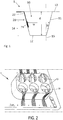
- a vessel 1 for performing electrochemical measurements is represented schematically in Fig. 1 , according to an embodiment.
- the vessel 1 comprises a well 10 for receiving a solution.
- the well 10 comprises an upper portion 13, a bottom portion 12 and a side wall portion 11, extending between the upper portion 13 and the bottom portion 12.
- the well comprises an electrode 20 on the side wall portion 11.
- the upper portion 13, the bottom portion 12 and the side wall portion 11 are formed integral, i.e., are made from one piece.
- the electrode 20 can be used to measure a specific analyte in a solution or to apply a stimuli such as an electric field to the solution of interest. Electrochemical measurement are particularly interesting for the continuous monitoring of cell culture media. Electroporation or impedance analysis are further applications that are frequently done on biological or chemical specimens
- the electrode 20 can comprise an active area 21 that is destined to be in contact with the solution when received in the well 10.
- the electrode 20 can also comprise a non-active area 22 that is insulated from said solution.
- the active area 21 extends in a predetermined portion 14 of the side wall portion 11, between the upper portion 13 down to the bottom portion 12.
- the non-active area 22 can correspond to electrical wires, insulated from said solution, to be connected to a measurement or to an electrical stimulation apparatus, eventually via a multiplexing electronic circuit.
- the non-active area 22 extends along the side wall portion 11 and the upper portion 13.
- the predetermined portion 14 can be in lower half of the well 10. Alternatively, the predetermined portion 14 can be in lower third of the well 10. More generally, the predetermined portion 14 can be in a region of the well 10 that is destined to be completely covered by the solution to be received in the well 10.
- the active area 21 of the electrode 20 is thus in contact with the solution and can react with it, for example via an electrochemical reaction.
- the active area 21 can be functionalized such that it can be used for measuring pH, for ion detection such as K + , NA + , Cl - , NH 4 + , PO 4 3- , or any other ion and salt detection, for enzymatic detection, for glucose, lactate, glutamate or other nutrient detection, or for electrochemical immunoassay for protein or antigen detection.
- ion detection such as K + , NA + , Cl - , NH 4 + , PO 4 3-
- any other ion and salt detection for enzymatic detection, for glucose, lactate, glutamate or other nutrient detection, or for electrochemical immunoassay for protein or antigen detection.
- the vessel can comprise a well 10 having a straight side wall portion 11, i.e., substantially perpendicular to the upper portion 13 (represented by the dotted line 15 in Fig. 1 ).
- the wall portion 11 can make an angle ⁇ relative to a straight wall portion.
- the angle ⁇ can be smaller than 45°, preferably smaller than 20° and even more preferably smaller than 10°.
- real geometries manufactured with high throughput methods will exhibit a rounded shape between the upper portion 13 and the side wall portion 11 of the vessel.
- the transition between the bottom portion 11 and the side wall portion 11 of the vessel can have a rounded shape.
- the vessel can comprise a well 10 having a ratio of the depth d over the width w of the well 10 is between 1 and 5, or between 2 and 3 or between 1 and 1.5 or between 0.5 and 1.
- the width w can be measured at mi-depth.
- the bottom portion 12 can be substantially flat as shown in Fig.1 , or can have any other suitable shape.
- the bottom portion 12 can have a concave shape.
- the well 10 can comprise more than one electrode 20 being located at least partially on the side wall portion 11.
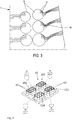
- Fig. 2 shows an example where the vessel 1, viewed form top, comprises a plurality of wells 10, each comprising three electrodes 20.
- the vessel 1 can be a multiwell plate, for example having a plurality of wells 10.
- the wells 10 can have a volume between 0.05 to 20 milliliters, and typically between 6 to 96 wells. Or substantially larger vessels up to 500 ml.
- the transparent thermoformed vessel 1 is located on a molding device 41 used in thermoforming.
- Fig. 5a represents a drawing of a planar foil 30 with six sets of electrodes 20. Each set is designated to be formed into one vessel. Each set of electrodes 20 is constituted of the number of electrodes needed for a desired analysis method. Single analyte measurement require two to four electrodes, whereas multi-analyte measurements may be done with a multitude of differently functionalized electrodes.
- the electrode 20 is placed at least partially on the side wall portion 11.
- the active area 21 of the electrode 20 is located on the side wall portion 11 and the non-active area 22 is running from the active area 21, on the side wall portion 11 and the upper portion 13, out of the well 10 for connection with a measurement apparatus (not shown).
- a vessel containing a large number of wells 10, such as a well-plate (or multiwell plate) can lead to a large number of electrodes to be contacted electrically to a measurement or to an electrical stimulation apparatus.
- a well-plate or multiwell plate
- an electrical multiplexing scheme such as an electrical switching matrix. This allows for limiting the number of electrical contacts to be made to the vessel and for limiting the number of electrical measurement and/or stimulation apparatus input/outputs.
- Such multiplexing is typically based on time division multiplexing.
- Fig. 3 shows another example of a multiwell plate 1, viewed form bottom, wherein the vessel 1 are made in a transparent plastic.
- the arrangement of the electrode 20 is the same as the one shown in Fig. 2 however the bottom portion 12 of the wells are concave and not flat as in Fig. 2 .
- the multiwell plate 1 of Fig. 3 shows that the arrangement of the active area 21 of the electrode 20 on the side wall portion 11 can enable for the bottom portion 12 to be transparent (the electrode 20 does not hamper the transparency of the bottom portion 12).
- the design of the at least one electrode can contain an active area 21 located at least partially at the bottom portion of the well. This can as an example improve the interaction between the at least active area 21 of an electrode and the well media. This can be of critical importance for cell culture vessels performing cell electro-stimulation or cell electro-impedance characterization.
- a method for manufacturing the vessel 1 comprises:
- thermoforming step comprises heating the substrate 30 to a temperature that allows the substrate 30 to be stretched into or onto the mold 40, and stretching the substrate 30 to a specific shape in the mold 40 to form the well 10.
- Fig. 4 illustrates a top view of a molding device 41 comprising four multiwell molding plates 101, 102, 103, 104, each comprising a plurality of well molds 40.
- the molding device 41 comprises a first multiwell molding plate 101 containing well molds 40 having a 1:1 aspect ratio and a concave-shaped bottom portion, a second multiwell molding plate 102 containing well molds 40 having a 2:3 aspect ratio and a concave-shaped bottom portion, a third multiwell molding plate 103 of well molds 40 having a 1:2 aspect ratio and a flat bottom portion with rounded edges, and a fourth multiwell molding plate 104 of well molds 40 having a 1:1 aspect ratio and a flat bottom portion with rounded edges.
- the resulting vessel 1 is a multiwell plate (not shown) comprising a first multiwell plate, conform to the multiwell molding plate 101, containing wells 10 having a 1:1 aspect ratio and a concave-shaped bottom portion 12, a second multiwell plate, conform to the second multiwell plate 102, containing wells 10 having a 2:3 aspect ratio and a concave-shaped bottom portion 12, a third multiwell plate, conform to the third multiwell molding plate 103, containing wells 10 having a 1:2 aspect ratio and a flat bottom portion 12 with rounded edges, and a fourth multiwell plate, conform to the fourth multiwell molding plate 104, containing wells 10 having a 1:1 aspect ratio and a flat bottom portion 12 with rounded edges.
- Fig. 5a represents a substrate 30 onto which several electrodes 20 have been printed.
- the substrate 30 can be a foil made of a material and having a thickness adapted for thermoforming.
- the substrate 30 can comprise a transparent or opaque thermoformable foil, such as polymethylmethacrylate (PMMA), cyclic olefin copolymer (COC), cyclo olefin polymers (COP), polycarbonate (PC), polystyrene (PS), polyethylene terephthalate (PET), polypropylene (PP), polyvinyl chloride (PVC), acrylonitrile butadiene styrene (ABS), polyethylenimine (PEI), polyamide (PI) and others suitable materials.
- PMMA polymethylmethacrylate
- COC cyclic olefin copolymer
- COP cyclo olefin polymers
- PC polycarbonate
- PS polystyrene
- PET polyethylene terephthalate
- Printing the electrode 20 can comprise printing a conductive metal ink on a surface of the substrate 30.
- Printing the electrode 20 can also comprise printing a conductive paste or a conductive carbon-based ink or paste, or printing a poly(3,4-ethylenedioxythiophene) polystyrene sulfonate (PEDOT:PSS) or printing any other organic conductive inks or pastes.
- PEDOT:PSS poly(3,4-ethylenedioxythiophene) polystyrene sulfonate
- the printing method can comprise screen printing, gravure printing, off-set printing, inkjet-printing, aerosol-jet printing, 3D printing, or any other suitable printing method.
- Thermoforming the (substantially flat) substrate 30 can comprise putting the substrate 30 on a molding device 41 (see Fig. 5c ).
- the molding device 41 is a plate comprising a plurality of molds 40.
- the substrate is heated and is then sucked into the molds 40 by means of vacuum suction.
- the vacuum suction can be provided through holes 42 provided in the bottom of the molds 40. Heating can be performed by using an infra-red heating source 60 or a hot air heating source 60.
- thermoforming step can be helped with a stamping press (not represented in the figures) having a shape conform with the one of the molds 40.
- a stamping press (not represented in the figures) having a shape conform with the one of the molds 40.
- the molding device and/or the stamping press can be heated.
- the substrate 30 should be configured for stretching (plastic deformation) below 500% and more preferably below 200% in both directions on areas where electrodes are located.
- This can be influenced and designed with the molding device geometry or by a stamping press geometry and its heating.
- Local stretching of the substrate 30 can as well be influenced by using a mask 50 (see Figs. 5b and 5c ) adapted for shielding at least a portion of the at least printed electrode, protecting predetermined areas of the substrate 30 from the heating source 60.
- Local stretching of the substrate 30 can also be influenced by local variation of the substrate thickness or substrate material.
- areas where electrode are located can contain an additional polymeric material having a higher stiffness or a higher glass-transition temperature.
- Local stretching of the substrate 30 can also be adapted locally, for example is the area where the electrode 20 is printed and/or areas of critical strain.
- the method for manufacturing can further comprise a step of functionalizing the electrode 20.
- step of functionalizing the electrode 20 comprises functionalizing the active area 21 of the electrode 20.
- the functionalization can comprise applying a silver chloride ink or paste.
- solution processed chemical agents can be added on top of any of the printed electrodes.
- the functionalization can comprise protein or antigen used in immunoassays or other biological molecules and compounds.
- the functionalization can compromise solution deposited membranes, solid state electrolytes or other electrochemical agents.
- the method of functionalization can comprise any printing technique, drop casting, physical vapor deposition or electrodeposition.
- the step of printing the electrode 20 and functionalizing the electrode 20 can be done on a roll to roll machine or sheet to sheet machine or roll to sheet machine.
- the functionalization or part of the functionalization can be done by a user, after the manufacturing of the vessel 1 is completed.
- the step of functionalizing is performed prior to thermoforming.
- the thermoforming step is preferably performed by using a mask 50 (see Figs. 5b and 5c ) adapted for shielding the active area 21 from the heat produced by the heating source 60.
- the shielding provided by the mask 50 is advantageous for protecting the delicate functionalization (e.g. biological enzyme) of the active area 21 from the heat.
- the mask 50 comprises a pattern of dots 51 opaque to the heat. The mask 50 is inserted between the heating source 60 and the substrate 30 in order to protect the active portion 21 of the electrodes 20 from the heat.
- Fig. 6 represents a cross-section view showing the formation of a single well 10 using the method of the invention.
- the substrate 30 is put over a mold 40 and a heating source 60 heats the substrate 30.
- the substantially planar substrate 30 comprised the printed electrode 20 containing an active area 21 and a non-active area 22.
- the substrate 30 is deformed into the mold 40 by the action of vacuum suction 70 at le bottom of the mold 40 (see Fig. 6b ).
- the deformation step takes place until the substrate 30 is completely deformed conform with the shape of the mold 40.
- the completely deformed substrate 30 then forms the well 10 comprising the upper portion 13, the bottom portion 12 and the side wall portion 11. Due to the placement of the electrode 20 printed on the substrate 30, the electrode 20 is located at least partially of the side wall portion 11 once the substrate 30 is completely deformed.
- the heating is in general stopped and a short cooling down time is used before demolding the vessel 1.
- Fig. 7 illustrates an example of positioning the printed electrodes 20 on the substrate 30 such that the active area 21 of the electrode 20 is properly located on the side wall portion 11 after the substrate 30 is thermoformed in the mold 40.
- six sets of electrodes 20 are equidistantly printed (three sets of three electrodes 20 and three sets of two electrodes 20, head to head) on the substrate 30 to form a six-well vessel 1.
- the electrode 20 comprises a non-active area 22 covered with an insulator 23 and an active area 21 located on the side wall portion 11 and destined to react with a solution received in the well 10.
- the electrode 20 also comprises a non-insulated portion 24 destined to be used as electrical connectors for a measurement and/or stimulation apparatus (not shown).
- the step of thermoforming the substrate 30 can be followed by a step of cutting the thermoformed substrate 30 to a final format.
- This cutting operation is optional and the final format can be obtained directly after the thermoforming step.
- the step of cutting can be performed before the thermoforming step.
- the manufacturing method can comprise a step of cutting the substrate 30 or one of its layer, containing the printed electrodes 20 to provide cut portions 25.
- a partially cut portion 25 can comprise an area comprising the electrode 20.
- An example of a cutting line is indicated by the numeral 26 around a printed electrode 20 in Fig. 8 .
- the step of providing the cut portions 25 can be performed between the step of printing the electrode 20 and the one of thermoforming the substrate 30.
- the substrate 30 with the cut portions 25 is put on the molding device 41, the substrate 30 is heated and the cut portions 25 are folded in the mold 40 such that the electrode 25 is located at least partially on the side wall portion 11 of the well 10.
- Folding the cut portions 25 can be performed by using a stamping press having a shape conform with the one of the mold 40. The vacuum suction may not be needed here.
- the folding of the cut portions 25 does not necessarily require any stretching of the substrate 30 (and/or the cut portions 25).
- the thickness of the substrate 30 can be locally varied (for example increased) in order to stiffen the substrate 30 where needed.
- the step of thermoforming the substrate 30 can be preceded by a step of thermoforming a first substrate (not shown), possibly not comprising electrode 20.
- the first substrate is heating to a temperature that allows the first substrate to be stretched into or onto the mold 40, and stretching the first substrate to a specific shape in the mold 40 to form the well 10.
- the cut portions 25 of the substrate 30 is then folded on the side wall portion 11 formed by the first substrate.
- the substrate can contain at least two layers. At least an uncut layer of the substrate will be molded in the well shape and hold the solution, while the cut layer(s) will be molded with minimal stretching of the electrodes.
- the cut portion 25 can experience a bending during the thermoforming process and not a two-dimensional stretching
- the substrate 30 comprising the cut portions 25 can be folded in an existing well 10 (for example a commercially available well, of a vessel, multiwell plate, etc., in order to add the electrode 20 on the side wall portion 11 of the well 10.
- the substrate 30 comprising the cut portions 25 can be folded on a culture flask, a disposable bioreactor flask, a petri dish, or any other suitable measurement vessel.
Landscapes
- Health & Medical Sciences (AREA)
- Chemical & Material Sciences (AREA)
- Life Sciences & Earth Sciences (AREA)
- Engineering & Computer Science (AREA)
- Immunology (AREA)
- General Health & Medical Sciences (AREA)
- Analytical Chemistry (AREA)
- Molecular Biology (AREA)
- Chemical Kinetics & Catalysis (AREA)
- Physics & Mathematics (AREA)
- Biochemistry (AREA)
- Pathology (AREA)
- General Physics & Mathematics (AREA)
- Electrochemistry (AREA)
- Hematology (AREA)
- Manufacturing & Machinery (AREA)
- Mechanical Engineering (AREA)
- Microelectronics & Electronic Packaging (AREA)
- Biomedical Technology (AREA)
- Urology & Nephrology (AREA)
- Clinical Laboratory Science (AREA)
- Medicinal Chemistry (AREA)
- Biotechnology (AREA)
- Food Science & Technology (AREA)
- Microbiology (AREA)
- Cell Biology (AREA)
- Apparatus Associated With Microorganisms And Enzymes (AREA)
- Sealing Battery Cases Or Jackets (AREA)
Applications Claiming Priority (1)
| Application Number | Priority Date | Filing Date | Title |
|---|---|---|---|
| EP17164486 | 2017-04-03 |
Publications (2)
| Publication Number | Publication Date |
|---|---|
| EP3384987A2 true EP3384987A2 (de) | 2018-10-10 |
| EP3384987A3 EP3384987A3 (de) | 2018-10-24 |
Family
ID=58488881
Family Applications (1)
| Application Number | Title | Priority Date | Filing Date |
|---|---|---|---|
| EP18165019.3A Withdrawn EP3384987A3 (de) | 2017-04-03 | 2018-03-29 | Gefäss zur durchführung elektrochemischer messungen und verfahren zur herstellung solch eines gefässes |
Country Status (2)
| Country | Link |
|---|---|
| US (1) | US20180284062A1 (de) |
| EP (1) | EP3384987A3 (de) |
Cited By (1)
| Publication number | Priority date | Publication date | Assignee | Title |
|---|---|---|---|---|
| TWI923980B (zh) | 2024-03-29 | 2026-05-01 | 樂協生醫股份有限公司 | 電化學測試片及電化學測試片的製造方法 |
Citations (1)
| Publication number | Priority date | Publication date | Assignee | Title |
|---|---|---|---|---|
| US20150125942A1 (en) | 2013-11-05 | 2015-05-07 | Axion Biosystems, Inc. | Devices, systems, and methods for targeted plating of materials in high-throughput culture plates |
Family Cites Families (10)
| Publication number | Priority date | Publication date | Assignee | Title |
|---|---|---|---|---|
| US5066372A (en) * | 1986-05-02 | 1991-11-19 | Ciba Corning Diagnostics Corp. | Unitary multiple electrode sensor |
| IL103674A0 (en) * | 1991-11-19 | 1993-04-04 | Houston Advanced Res Center | Method and apparatus for molecule detection |
| DE10023015A1 (de) * | 2000-05-05 | 2002-01-24 | Inst Chemo Biosensorik | Verdahren zur Herstellung eines dreidimensionalen Sensorelementes |
| US6519835B1 (en) * | 2000-08-18 | 2003-02-18 | Watlow Polymer Technologies | Method of formable thermoplastic laminate heated element assembly |
| US7182853B2 (en) * | 2000-09-22 | 2007-02-27 | University Of Dayton | Redox control/monitoring platform for high throughput screening/drug discovery applications |
| US8057903B2 (en) * | 2001-11-30 | 2011-11-15 | Sabic Innovative Plastics Ip B.V. | Multilayer articles comprising resorcinol arylate polyester and method for making thereof |
| GB2386949A (en) * | 2002-03-26 | 2003-10-01 | Sensor Tech Ltd | A multiwell plate for electrochemical detection |
| GB2445738A (en) * | 2007-01-16 | 2008-07-23 | Lab901 Ltd | Microfluidic device |
| DE102009014902A1 (de) * | 2009-03-25 | 2010-10-07 | Siemens Aktiengesellschaft | Helicobacter pylori-Sensor |
| EP2811299A1 (de) * | 2013-06-07 | 2014-12-10 | Roche Diagniostics GmbH | Testelement zur Detektion von mindestens einem Analyten in einer Körperflüssigkeit |
-
2018
- 2018-03-29 EP EP18165019.3A patent/EP3384987A3/de not_active Withdrawn
- 2018-04-02 US US15/942,632 patent/US20180284062A1/en not_active Abandoned
Patent Citations (1)
| Publication number | Priority date | Publication date | Assignee | Title |
|---|---|---|---|---|
| US20150125942A1 (en) | 2013-11-05 | 2015-05-07 | Axion Biosystems, Inc. | Devices, systems, and methods for targeted plating of materials in high-throughput culture plates |
Cited By (1)
| Publication number | Priority date | Publication date | Assignee | Title |
|---|---|---|---|---|
| TWI923980B (zh) | 2024-03-29 | 2026-05-01 | 樂協生醫股份有限公司 | 電化學測試片及電化學測試片的製造方法 |
Also Published As
| Publication number | Publication date |
|---|---|
| EP3384987A3 (de) | 2018-10-24 |
| US20180284062A1 (en) | 2018-10-04 |
Similar Documents
| Publication | Publication Date | Title |
|---|---|---|
| Yu et al. | Pressure-based biosensor integrated with a flexible pressure sensor and an electrochromic device for visual detection | |
| US8138496B2 (en) | Addressable transistor chip for conducting assays | |
| CN103210309A (zh) | 具有三维结构的生物传感器及其制造方法 | |
| EP3045902A1 (de) | Sensor mit Elektrolyt-Gate zum Speziesnachweis | |
| US10480091B2 (en) | Sensors and methods of manufacture thereof | |
| Pradela-Filho et al. | Patterning (electro) chemical treatment-free electrodes with a 3D printing pen | |
| US20160103096A1 (en) | Biochemical test chip and method for manufacturing the same | |
| EP3384987A2 (de) | Gefäss zur durchführung elektrochemischer messungen und verfahren zur herstellung solch eines gefässes | |
| CN107076730A (zh) | 电阻结构、电阻结构单元、辨认信息装置及生物传感器 | |
| CN108226249B (zh) | 一次性纳米孔生物传感器及其制作方法 | |
| Gabardo et al. | A New Wrinkle in Biosensors: Wrinkled electrodes could be a breakthrough for lab-on-a-chip devices | |
| CN112378972A (zh) | 一种具有高稳定性的无标识生物传感器及其制作方法 | |
| CN201497726U (zh) | 生物传感器 | |
| EP3818361B1 (de) | Vorrichtungen und verfahren zur topografisch geführten zellmigration | |
| CN206459991U (zh) | 生物传感器 | |
| CN109044327A (zh) | 一种刺入力度可控的微针干式电极 | |
| EP2806971B1 (de) | Patrone und methode zur verarbeitung einer flüssigkeit | |
| JP6612651B2 (ja) | バイオセンサチップの製造方法 | |
| US20140151220A1 (en) | Electrochemical Sensing Strip | |
| JP2011215010A (ja) | バイオセンサチップ組立用キット、バイオセンサチップの製造方法及びバイオセンサチップ | |
| KR20120138082A (ko) | 바이오 칩 | |
| Park et al. | Through-Layer Contact with Encapsulated Graphene Using One-Step Laser Scribing | |
| EP4417737A1 (de) | Potentialgesteuerte multisensing-elektronikmikrotiterplatte | |
| CN115249553B (zh) | 一种柔性电极的制备方法 | |
| CN104034767A (zh) | 辨认信息装置及生物传感器 |
Legal Events
| Date | Code | Title | Description |
|---|---|---|---|
| PUAI | Public reference made under article 153(3) epc to a published international application that has entered the european phase |
Free format text: ORIGINAL CODE: 0009012 |
|
| STAA | Information on the status of an ep patent application or granted ep patent |
Free format text: STATUS: THE APPLICATION HAS BEEN PUBLISHED |
|
| PUAL | Search report despatched |
Free format text: ORIGINAL CODE: 0009013 |
|
| AK | Designated contracting states |
Kind code of ref document: A2 Designated state(s): AL AT BE BG CH CY CZ DE DK EE ES FI FR GB GR HR HU IE IS IT LI LT LU LV MC MK MT NL NO PL PT RO RS SE SI SK SM TR |
|
| AX | Request for extension of the european patent |
Extension state: BA ME |
|
| AK | Designated contracting states |
Kind code of ref document: A3 Designated state(s): AL AT BE BG CH CY CZ DE DK EE ES FI FR GB GR HR HU IE IS IT LI LT LU LV MC MK MT NL NO PL PT RO RS SE SI SK SM TR |
|
| AX | Request for extension of the european patent |
Extension state: BA ME |
|
| RIC1 | Information provided on ipc code assigned before grant |
Ipc: B29C 51/10 20060101ALI20180918BHEP Ipc: B29C 51/12 20060101ALI20180918BHEP Ipc: G01N 27/403 20060101ALI20180918BHEP Ipc: B01L 3/00 20060101AFI20180918BHEP Ipc: G01N 27/28 20060101ALI20180918BHEP Ipc: H05K 3/00 20060101ALI20180918BHEP |
|
| STAA | Information on the status of an ep patent application or granted ep patent |
Free format text: STATUS: REQUEST FOR EXAMINATION WAS MADE |
|
| 17P | Request for examination filed |
Effective date: 20190318 |
|
| RBV | Designated contracting states (corrected) |
Designated state(s): AL AT BE BG CH CY CZ DE DK EE ES FI FR GB GR HR HU IE IS IT LI LT LU LV MC MK MT NL NO PL PT RO RS SE SI SK SM TR |
|
| STAA | Information on the status of an ep patent application or granted ep patent |
Free format text: STATUS: EXAMINATION IS IN PROGRESS |
|
| 17Q | First examination report despatched |
Effective date: 20190618 |
|
| STAA | Information on the status of an ep patent application or granted ep patent |
Free format text: STATUS: THE APPLICATION IS DEEMED TO BE WITHDRAWN |
|
| 18D | Application deemed to be withdrawn |
Effective date: 20220903 |