EP3381069B1 - Procédé d'obtention d'un semi-conducteur organique de type n ou de type p par irradiation uv-vis - Google Patents
Procédé d'obtention d'un semi-conducteur organique de type n ou de type p par irradiation uv-vis Download PDFInfo
- Publication number
- EP3381069B1 EP3381069B1 EP16805994.7A EP16805994A EP3381069B1 EP 3381069 B1 EP3381069 B1 EP 3381069B1 EP 16805994 A EP16805994 A EP 16805994A EP 3381069 B1 EP3381069 B1 EP 3381069B1
- Authority
- EP
- European Patent Office
- Prior art keywords
- type
- organic semiconductor
- process according
- type semiconducting
- cnts
- Prior art date
- Legal status (The legal status is an assumption and is not a legal conclusion. Google has not performed a legal analysis and makes no representation as to the accuracy of the status listed.)
- Not-in-force
Links
- 238000000034 method Methods 0.000 title claims description 48
- 239000004065 semiconductor Substances 0.000 title claims description 48
- 230000008569 process Effects 0.000 title claims description 40
- 239000002041 carbon nanotube Substances 0.000 claims description 76
- -1 polyethylene terephthalate Polymers 0.000 claims description 47
- 239000002086 nanomaterial Substances 0.000 claims description 39
- 229920000301 poly(3-hexylthiophene-2,5-diyl) polymer Polymers 0.000 claims description 33
- 239000000758 substrate Substances 0.000 claims description 28
- OKTJSMMVPCPJKN-UHFFFAOYSA-N Carbon Chemical compound [C] OKTJSMMVPCPJKN-UHFFFAOYSA-N 0.000 claims description 20
- 238000000151 deposition Methods 0.000 claims description 15
- 239000002904 solvent Substances 0.000 claims description 15
- 239000000203 mixture Substances 0.000 claims description 13
- 239000002070 nanowire Substances 0.000 claims description 13
- 230000005855 radiation Effects 0.000 claims description 13
- 229920002873 Polyethylenimine Polymers 0.000 claims description 12
- ZOXJGFHDIHLPTG-UHFFFAOYSA-N Boron Chemical compound [B] ZOXJGFHDIHLPTG-UHFFFAOYSA-N 0.000 claims description 11
- 229910052796 boron Inorganic materials 0.000 claims description 11
- 229920000139 polyethylene terephthalate Polymers 0.000 claims description 10
- 239000005020 polyethylene terephthalate Substances 0.000 claims description 10
- 239000012298 atmosphere Substances 0.000 claims description 8
- QVGXLLKOCUKJST-UHFFFAOYSA-N atomic oxygen Chemical compound [O] QVGXLLKOCUKJST-UHFFFAOYSA-N 0.000 claims description 8
- 229910021389 graphene Inorganic materials 0.000 claims description 8
- 229910052760 oxygen Inorganic materials 0.000 claims description 8
- 239000001301 oxygen Substances 0.000 claims description 8
- WGTYBPLFGIVFAS-UHFFFAOYSA-M tetramethylammonium hydroxide Chemical compound [OH-].C[N+](C)(C)C WGTYBPLFGIVFAS-UHFFFAOYSA-M 0.000 claims description 8
- LVEYOSJUKRVCCF-UHFFFAOYSA-N 1,3-bis(diphenylphosphino)propane Chemical compound C=1C=CC=CC=1P(C=1C=CC=CC=1)CCCP(C=1C=CC=CC=1)C1=CC=CC=C1 LVEYOSJUKRVCCF-UHFFFAOYSA-N 0.000 claims description 6
- 239000002033 PVDF binder Substances 0.000 claims description 6
- 239000004698 Polyethylene Substances 0.000 claims description 6
- 239000004743 Polypropylene Substances 0.000 claims description 6
- 239000006185 dispersion Substances 0.000 claims description 6
- 229910002804 graphite Inorganic materials 0.000 claims description 6
- 239000010439 graphite Substances 0.000 claims description 6
- 230000001678 irradiating effect Effects 0.000 claims description 6
- 239000002064 nanoplatelet Substances 0.000 claims description 6
- 239000002074 nanoribbon Substances 0.000 claims description 6
- 229920000573 polyethylene Polymers 0.000 claims description 6
- 229920001155 polypropylene Polymers 0.000 claims description 6
- 229920001343 polytetrafluoroethylene Polymers 0.000 claims description 6
- 239000004810 polytetrafluoroethylene Substances 0.000 claims description 6
- 229920000915 polyvinyl chloride Polymers 0.000 claims description 6
- 239000004800 polyvinyl chloride Substances 0.000 claims description 6
- 229920002981 polyvinylidene fluoride Polymers 0.000 claims description 6
- 229910021393 carbon nanotube Inorganic materials 0.000 claims description 5
- 239000002048 multi walled nanotube Substances 0.000 claims description 5
- CBXRMKZFYQISIV-UHFFFAOYSA-N 1-n,1-n,1-n',1-n',2-n,2-n,2-n',2-n'-octamethylethene-1,1,2,2-tetramine Chemical group CN(C)C(N(C)C)=C(N(C)C)N(C)C CBXRMKZFYQISIV-UHFFFAOYSA-N 0.000 claims description 4
- XMWRBQBLMFGWIX-UHFFFAOYSA-N C60 fullerene Chemical class C12=C3C(C4=C56)=C7C8=C5C5=C9C%10=C6C6=C4C1=C1C4=C6C6=C%10C%10=C9C9=C%11C5=C8C5=C8C7=C3C3=C7C2=C1C1=C2C4=C6C4=C%10C6=C9C9=C%11C5=C5C8=C3C3=C7C1=C1C2=C4C6=C2C9=C5C3=C12 XMWRBQBLMFGWIX-UHFFFAOYSA-N 0.000 claims description 4
- RPNUMPOLZDHAAY-UHFFFAOYSA-N Diethylenetriamine Chemical compound NCCNCCN RPNUMPOLZDHAAY-UHFFFAOYSA-N 0.000 claims description 4
- 239000004642 Polyimide Substances 0.000 claims description 4
- 239000004793 Polystyrene Substances 0.000 claims description 4
- XLOMVQKBTHCTTD-UHFFFAOYSA-N Zinc monoxide Chemical compound [Zn]=O XLOMVQKBTHCTTD-UHFFFAOYSA-N 0.000 claims description 4
- 239000002079 double walled nanotube Substances 0.000 claims description 4
- 238000001035 drying Methods 0.000 claims description 4
- 229910003472 fullerene Inorganic materials 0.000 claims description 4
- VNWKTOKETHGBQD-UHFFFAOYSA-N methane Chemical compound C VNWKTOKETHGBQD-UHFFFAOYSA-N 0.000 claims description 4
- 239000011112 polyethylene naphthalate Substances 0.000 claims description 4
- 229920001721 polyimide Polymers 0.000 claims description 4
- RIOQSEWOXXDEQQ-UHFFFAOYSA-N triphenylphosphine Chemical compound C1=CC=CC=C1P(C=1C=CC=CC=1)C1=CC=CC=C1 RIOQSEWOXXDEQQ-UHFFFAOYSA-N 0.000 claims description 4
- XUIMIQQOPSSXEZ-UHFFFAOYSA-N Silicon Chemical compound [Si] XUIMIQQOPSSXEZ-UHFFFAOYSA-N 0.000 claims description 3
- 229920000553 poly(phenylenevinylene) Polymers 0.000 claims description 3
- 229920000767 polyaniline Polymers 0.000 claims description 3
- 229910052710 silicon Inorganic materials 0.000 claims description 3
- 239000010703 silicon Substances 0.000 claims description 3
- 239000004094 surface-active agent Substances 0.000 claims description 3
- 229910002899 Bi2Te3 Inorganic materials 0.000 claims description 2
- XOJVVFBFDXDTEG-UHFFFAOYSA-N Norphytane Natural products CC(C)CCCC(C)CCCC(C)CCCC(C)C XOJVVFBFDXDTEG-UHFFFAOYSA-N 0.000 claims description 2
- 229910002665 PbTe Inorganic materials 0.000 claims description 2
- OAICVXFJPJFONN-UHFFFAOYSA-N Phosphorus Chemical compound [P] OAICVXFJPJFONN-UHFFFAOYSA-N 0.000 claims description 2
- 229920000291 Poly(9,9-dioctylfluorene) Polymers 0.000 claims description 2
- GWEVSGVZZGPLCZ-UHFFFAOYSA-N Titan oxide Chemical compound O=[Ti]=O GWEVSGVZZGPLCZ-UHFFFAOYSA-N 0.000 claims description 2
- HSFWRNGVRCDJHI-UHFFFAOYSA-N alpha-acetylene Natural products C#C HSFWRNGVRCDJHI-UHFFFAOYSA-N 0.000 claims description 2
- 238000001704 evaporation Methods 0.000 claims description 2
- 229910052698 phosphorus Inorganic materials 0.000 claims description 2
- 239000011574 phosphorus Substances 0.000 claims description 2
- 229920001197 polyacetylene Polymers 0.000 claims description 2
- 229920002098 polyfluorene Polymers 0.000 claims description 2
- OCGWQDWYSQAFTO-UHFFFAOYSA-N tellanylidenelead Chemical compound [Pb]=[Te] OCGWQDWYSQAFTO-UHFFFAOYSA-N 0.000 claims description 2
- 229910052714 tellurium Inorganic materials 0.000 claims description 2
- PORWMNRCUJJQNO-UHFFFAOYSA-N tellurium atom Chemical compound [Te] PORWMNRCUJJQNO-UHFFFAOYSA-N 0.000 claims description 2
- PCCVSPMFGIFTHU-UHFFFAOYSA-N tetracyanoquinodimethane Chemical compound N#CC(C#N)=C1C=CC(=C(C#N)C#N)C=C1 PCCVSPMFGIFTHU-UHFFFAOYSA-N 0.000 claims description 2
- FHCPAXDKURNIOZ-UHFFFAOYSA-N tetrathiafulvalene Chemical compound S1C=CSC1=C1SC=CS1 FHCPAXDKURNIOZ-UHFFFAOYSA-N 0.000 claims description 2
- OGIDPMRJRNCKJF-UHFFFAOYSA-N titanium oxide Inorganic materials [Ti]=O OGIDPMRJRNCKJF-UHFFFAOYSA-N 0.000 claims description 2
- 239000011787 zinc oxide Substances 0.000 claims description 2
- 229920003207 poly(ethylene-2,6-naphthalate) Polymers 0.000 claims 2
- 229920002223 polystyrene Polymers 0.000 claims 2
- 229920002635 polyurethane Polymers 0.000 claims 2
- 239000004814 polyurethane Substances 0.000 claims 2
- 239000002131 composite material Substances 0.000 description 27
- 239000000243 solution Substances 0.000 description 23
- 239000000463 material Substances 0.000 description 20
- IJGRMHOSHXDMSA-UHFFFAOYSA-N Atomic nitrogen Chemical compound N#N IJGRMHOSHXDMSA-UHFFFAOYSA-N 0.000 description 16
- RFFLAFLAYFXFSW-UHFFFAOYSA-N 1,2-dichlorobenzene Chemical compound ClC1=CC=CC=C1Cl RFFLAFLAYFXFSW-UHFFFAOYSA-N 0.000 description 15
- 239000002253 acid Substances 0.000 description 13
- 229920000642 polymer Polymers 0.000 description 13
- 238000005259 measurement Methods 0.000 description 11
- 238000011282 treatment Methods 0.000 description 11
- HEDRZPFGACZZDS-UHFFFAOYSA-N Chloroform Chemical compound ClC(Cl)Cl HEDRZPFGACZZDS-UHFFFAOYSA-N 0.000 description 10
- XEEYBQQBJWHFJM-UHFFFAOYSA-N Iron Chemical compound [Fe] XEEYBQQBJWHFJM-UHFFFAOYSA-N 0.000 description 10
- 238000010521 absorption reaction Methods 0.000 description 10
- 238000004630 atomic force microscopy Methods 0.000 description 9
- 230000008021 deposition Effects 0.000 description 9
- 238000002360 preparation method Methods 0.000 description 9
- 239000010410 layer Substances 0.000 description 8
- 229910052757 nitrogen Inorganic materials 0.000 description 8
- 239000002114 nanocomposite Substances 0.000 description 7
- 238000009281 ultraviolet germicidal irradiation Methods 0.000 description 7
- PBKONEOXTCPAFI-UHFFFAOYSA-N 1,2,4-trichlorobenzene Chemical compound ClC1=CC=C(Cl)C(Cl)=C1 PBKONEOXTCPAFI-UHFFFAOYSA-N 0.000 description 6
- LFQSCWFLJHTTHZ-UHFFFAOYSA-N Ethanol Chemical compound CCO LFQSCWFLJHTTHZ-UHFFFAOYSA-N 0.000 description 6
- OKKJLVBELUTLKV-UHFFFAOYSA-N Methanol Chemical compound OC OKKJLVBELUTLKV-UHFFFAOYSA-N 0.000 description 6
- YXFVVABEGXRONW-UHFFFAOYSA-N Toluene Chemical compound CC1=CC=CC=C1 YXFVVABEGXRONW-UHFFFAOYSA-N 0.000 description 6
- 239000000969 carrier Substances 0.000 description 6
- 238000005325 percolation Methods 0.000 description 6
- 238000005424 photoluminescence Methods 0.000 description 6
- 238000012512 characterization method Methods 0.000 description 5
- 230000007423 decrease Effects 0.000 description 5
- 229910052742 iron Inorganic materials 0.000 description 5
- 238000004519 manufacturing process Methods 0.000 description 5
- 238000000172 transmission X-ray microscopy Methods 0.000 description 5
- KFZMGEQAYNKOFK-UHFFFAOYSA-N Isopropanol Chemical compound CC(C)O KFZMGEQAYNKOFK-UHFFFAOYSA-N 0.000 description 4
- CTQNGGLPUBDAKN-UHFFFAOYSA-N O-Xylene Chemical group CC1=CC=CC=C1C CTQNGGLPUBDAKN-UHFFFAOYSA-N 0.000 description 4
- URLKBWYHVLBVBO-UHFFFAOYSA-N Para-Xylene Chemical group CC1=CC=C(C)C=C1 URLKBWYHVLBVBO-UHFFFAOYSA-N 0.000 description 4
- 230000005540 biological transmission Effects 0.000 description 4
- MVPPADPHJFYWMZ-UHFFFAOYSA-N chlorobenzene Chemical compound ClC1=CC=CC=C1 MVPPADPHJFYWMZ-UHFFFAOYSA-N 0.000 description 4
- 238000001124 conductive atomic force microscopy Methods 0.000 description 4
- 230000000694 effects Effects 0.000 description 4
- 239000005457 ice water Substances 0.000 description 4
- 238000001000 micrograph Methods 0.000 description 4
- 230000003287 optical effect Effects 0.000 description 4
- WEVYAHXRMPXWCK-UHFFFAOYSA-N Acetonitrile Chemical compound CC#N WEVYAHXRMPXWCK-UHFFFAOYSA-N 0.000 description 3
- 239000000654 additive Substances 0.000 description 3
- 230000015556 catabolic process Effects 0.000 description 3
- 230000008859 change Effects 0.000 description 3
- 238000006731 degradation reaction Methods 0.000 description 3
- 239000011521 glass Substances 0.000 description 3
- 238000007641 inkjet printing Methods 0.000 description 3
- 239000008188 pellet Substances 0.000 description 3
- 238000010791 quenching Methods 0.000 description 3
- 230000000171 quenching effect Effects 0.000 description 3
- 238000001878 scanning electron micrograph Methods 0.000 description 3
- 238000004626 scanning electron microscopy Methods 0.000 description 3
- OCJBOOLMMGQPQU-UHFFFAOYSA-N 1,4-dichlorobenzene Chemical compound ClC1=CC=C(Cl)C=C1 OCJBOOLMMGQPQU-UHFFFAOYSA-N 0.000 description 2
- 229920000742 Cotton Polymers 0.000 description 2
- 238000005033 Fourier transform infrared spectroscopy Methods 0.000 description 2
- 239000004677 Nylon Substances 0.000 description 2
- 238000001237 Raman spectrum Methods 0.000 description 2
- BQCADISMDOOEFD-UHFFFAOYSA-N Silver Chemical compound [Ag] BQCADISMDOOEFD-UHFFFAOYSA-N 0.000 description 2
- 239000004809 Teflon Substances 0.000 description 2
- 229920006362 Teflon® Polymers 0.000 description 2
- YTPLMLYBLZKORZ-UHFFFAOYSA-N Thiophene Chemical group C=1C=CSC=1 YTPLMLYBLZKORZ-UHFFFAOYSA-N 0.000 description 2
- 230000000996 additive effect Effects 0.000 description 2
- 230000002776 aggregation Effects 0.000 description 2
- 238000013019 agitation Methods 0.000 description 2
- 238000005102 attenuated total reflection Methods 0.000 description 2
- 229910052799 carbon Inorganic materials 0.000 description 2
- 238000005266 casting Methods 0.000 description 2
- 239000003054 catalyst Substances 0.000 description 2
- 239000000919 ceramic Substances 0.000 description 2
- 238000005229 chemical vapour deposition Methods 0.000 description 2
- 239000011248 coating agent Substances 0.000 description 2
- 238000000576 coating method Methods 0.000 description 2
- 230000000295 complement effect Effects 0.000 description 2
- 150000001875 compounds Chemical class 0.000 description 2
- 239000004567 concrete Substances 0.000 description 2
- 229920000547 conjugated polymer Polymers 0.000 description 2
- 230000021615 conjugation Effects 0.000 description 2
- 239000002019 doping agent Substances 0.000 description 2
- 229920001971 elastomer Polymers 0.000 description 2
- 238000005516 engineering process Methods 0.000 description 2
- 230000005284 excitation Effects 0.000 description 2
- 238000001914 filtration Methods 0.000 description 2
- 229910052500 inorganic mineral Inorganic materials 0.000 description 2
- 239000010985 leather Substances 0.000 description 2
- 238000004768 lowest unoccupied molecular orbital Methods 0.000 description 2
- 239000011159 matrix material Substances 0.000 description 2
- 229910052751 metal Inorganic materials 0.000 description 2
- 239000002184 metal Substances 0.000 description 2
- 239000011707 mineral Substances 0.000 description 2
- 239000002105 nanoparticle Substances 0.000 description 2
- 229920001778 nylon Polymers 0.000 description 2
- 229940078552 o-xylene Drugs 0.000 description 2
- 238000000879 optical micrograph Methods 0.000 description 2
- 238000000059 patterning Methods 0.000 description 2
- 238000000103 photoluminescence spectrum Methods 0.000 description 2
- BASFCYQUMIYNBI-UHFFFAOYSA-N platinum Chemical compound [Pt] BASFCYQUMIYNBI-UHFFFAOYSA-N 0.000 description 2
- 229910052709 silver Inorganic materials 0.000 description 2
- 239000004332 silver Substances 0.000 description 2
- 239000002109 single walled nanotube Substances 0.000 description 2
- 150000003384 small molecules Chemical class 0.000 description 2
- 238000000527 sonication Methods 0.000 description 2
- 238000001228 spectrum Methods 0.000 description 2
- 238000005507 spraying Methods 0.000 description 2
- 230000003746 surface roughness Effects 0.000 description 2
- 239000004753 textile Substances 0.000 description 2
- 238000012876 topography Methods 0.000 description 2
- XLYOFNOQVPJJNP-UHFFFAOYSA-N water Substances O XLYOFNOQVPJJNP-UHFFFAOYSA-N 0.000 description 2
- 239000002023 wood Substances 0.000 description 2
- YBJHBAHKTGYVGT-ZKWXMUAHSA-N (+)-Biotin Chemical compound N1C(=O)N[C@@H]2[C@H](CCCCC(=O)O)SC[C@@H]21 YBJHBAHKTGYVGT-ZKWXMUAHSA-N 0.000 description 1
- RYAUSSKQMZRMAI-YESZJQIVSA-N (S)-fenpropimorph Chemical compound C([C@@H](C)CC=1C=CC(=CC=1)C(C)(C)C)N1C[C@H](C)O[C@H](C)C1 RYAUSSKQMZRMAI-YESZJQIVSA-N 0.000 description 1
- 229920001817 Agar Polymers 0.000 description 1
- 241000252073 Anguilliformes Species 0.000 description 1
- 229910001006 Constantan Inorganic materials 0.000 description 1
- RYGMFSIKBFXOCR-UHFFFAOYSA-N Copper Chemical compound [Cu] RYGMFSIKBFXOCR-UHFFFAOYSA-N 0.000 description 1
- 238000001157 Fourier transform infrared spectrum Methods 0.000 description 1
- 230000005355 Hall effect Effects 0.000 description 1
- 238000004566 IR spectroscopy Methods 0.000 description 1
- CBENFWSGALASAD-UHFFFAOYSA-N Ozone Chemical compound [O-][O+]=O CBENFWSGALASAD-UHFFFAOYSA-N 0.000 description 1
- 238000001069 Raman spectroscopy Methods 0.000 description 1
- 230000005678 Seebeck effect Effects 0.000 description 1
- 238000002835 absorbance Methods 0.000 description 1
- 230000002730 additional effect Effects 0.000 description 1
- 239000008272 agar Substances 0.000 description 1
- 238000005054 agglomeration Methods 0.000 description 1
- 238000004220 aggregation Methods 0.000 description 1
- 125000000217 alkyl group Chemical group 0.000 description 1
- 238000004458 analytical method Methods 0.000 description 1
- 230000015572 biosynthetic process Effects 0.000 description 1
- 239000002800 charge carrier Substances 0.000 description 1
- 239000004020 conductor Substances 0.000 description 1
- 229910052802 copper Inorganic materials 0.000 description 1
- 239000010949 copper Substances 0.000 description 1
- 238000005520 cutting process Methods 0.000 description 1
- 230000032798 delamination Effects 0.000 description 1
- 230000003292 diminished effect Effects 0.000 description 1
- 238000003618 dip coating Methods 0.000 description 1
- 238000005430 electron energy loss spectroscopy Methods 0.000 description 1
- 238000002474 experimental method Methods 0.000 description 1
- KTWOOEGAPBSYNW-UHFFFAOYSA-N ferrocene Chemical compound [Fe+2].C=1C=C[CH-]C=1.C=1C=C[CH-]C=1 KTWOOEGAPBSYNW-UHFFFAOYSA-N 0.000 description 1
- 239000000945 filler Substances 0.000 description 1
- 238000007646 gravure printing Methods 0.000 description 1
- 238000003306 harvesting Methods 0.000 description 1
- 238000010438 heat treatment Methods 0.000 description 1
- 238000007731 hot pressing Methods 0.000 description 1
- 230000003993 interaction Effects 0.000 description 1
- QSHDDOUJBYECFT-UHFFFAOYSA-N mercury Chemical compound [Hg] QSHDDOUJBYECFT-UHFFFAOYSA-N 0.000 description 1
- VYQNWZOUAUKGHI-UHFFFAOYSA-N monobenzone Chemical compound C1=CC(O)=CC=C1OCC1=CC=CC=C1 VYQNWZOUAUKGHI-UHFFFAOYSA-N 0.000 description 1
- 239000002071 nanotube Substances 0.000 description 1
- 125000004433 nitrogen atom Chemical group N* 0.000 description 1
- 238000000399 optical microscopy Methods 0.000 description 1
- 239000011368 organic material Substances 0.000 description 1
- 230000003647 oxidation Effects 0.000 description 1
- 238000007254 oxidation reaction Methods 0.000 description 1
- 229910052697 platinum Inorganic materials 0.000 description 1
- 229920000867 polyelectrolyte Polymers 0.000 description 1
- 239000002244 precipitate Substances 0.000 description 1
- 238000007639 printing Methods 0.000 description 1
- 230000009467 reduction Effects 0.000 description 1
- 239000012047 saturated solution Substances 0.000 description 1
- 238000007650 screen-printing Methods 0.000 description 1
- 239000002356 single layer Substances 0.000 description 1
- 238000007764 slot die coating Methods 0.000 description 1
- 239000007787 solid Substances 0.000 description 1
- 239000000126 substance Substances 0.000 description 1
- 238000003786 synthesis reaction Methods 0.000 description 1
- 229930192474 thiophene Natural products 0.000 description 1
- 230000007704 transition Effects 0.000 description 1
- 238000000411 transmission spectrum Methods 0.000 description 1
- FEPMHVLSLDOMQC-UHFFFAOYSA-N virginiamycin-S1 Natural products CC1OC(=O)C(C=2C=CC=CC=2)NC(=O)C2CC(=O)CCN2C(=O)C(CC=2C=CC=CC=2)N(C)C(=O)C2CCCN2C(=O)C(CC)NC(=O)C1NC(=O)C1=NC=CC=C1O FEPMHVLSLDOMQC-UHFFFAOYSA-N 0.000 description 1
- 239000002918 waste heat Substances 0.000 description 1
Images


Classifications
-
- H—ELECTRICITY
- H10—SEMICONDUCTOR DEVICES; ELECTRIC SOLID-STATE DEVICES NOT OTHERWISE PROVIDED FOR
- H10K—ORGANIC ELECTRIC SOLID-STATE DEVICES
- H10K71/00—Manufacture or treatment specially adapted for the organic devices covered by this subclass
- H10K71/30—Doping active layers, e.g. electron transporting layers
-
- H—ELECTRICITY
- H10—SEMICONDUCTOR DEVICES; ELECTRIC SOLID-STATE DEVICES NOT OTHERWISE PROVIDED FOR
- H10N—ELECTRIC SOLID-STATE DEVICES NOT OTHERWISE PROVIDED FOR
- H10N10/00—Thermoelectric devices comprising a junction of dissimilar materials, i.e. devices exhibiting Seebeck or Peltier effects
- H10N10/80—Constructional details
- H10N10/85—Thermoelectric active materials
- H10N10/856—Thermoelectric active materials comprising organic compositions
-
- H—ELECTRICITY
- H10—SEMICONDUCTOR DEVICES; ELECTRIC SOLID-STATE DEVICES NOT OTHERWISE PROVIDED FOR
- H10K—ORGANIC ELECTRIC SOLID-STATE DEVICES
- H10K85/00—Organic materials used in the body or electrodes of devices covered by this subclass
- H10K85/10—Organic polymers or oligomers
- H10K85/111—Organic polymers or oligomers comprising aromatic, heteroaromatic, or aryl chains, e.g. polyaniline, polyphenylene or polyphenylene vinylene
- H10K85/113—Heteroaromatic compounds comprising sulfur or selene, e.g. polythiophene
-
- H—ELECTRICITY
- H10—SEMICONDUCTOR DEVICES; ELECTRIC SOLID-STATE DEVICES NOT OTHERWISE PROVIDED FOR
- H10K—ORGANIC ELECTRIC SOLID-STATE DEVICES
- H10K85/00—Organic materials used in the body or electrodes of devices covered by this subclass
- H10K85/10—Organic polymers or oligomers
- H10K85/141—Organic polymers or oligomers comprising aliphatic or olefinic chains, e.g. poly N-vinylcarbazol, PVC or PTFE
-
- H—ELECTRICITY
- H10—SEMICONDUCTOR DEVICES; ELECTRIC SOLID-STATE DEVICES NOT OTHERWISE PROVIDED FOR
- H10K—ORGANIC ELECTRIC SOLID-STATE DEVICES
- H10K85/00—Organic materials used in the body or electrodes of devices covered by this subclass
- H10K85/20—Carbon compounds, e.g. carbon nanotubes or fullerenes
- H10K85/221—Carbon nanotubes
-
- H—ELECTRICITY
- H10—SEMICONDUCTOR DEVICES; ELECTRIC SOLID-STATE DEVICES NOT OTHERWISE PROVIDED FOR
- H10K—ORGANIC ELECTRIC SOLID-STATE DEVICES
- H10K2102/00—Constructional details relating to the organic devices covered by this subclass
- H10K2102/301—Details of OLEDs
- H10K2102/331—Nanoparticles used in non-emissive layers, e.g. in packaging layer
Definitions
- the invention relates to a process of obtainment of an n-type or a p-type organic semiconductor by irradiating a p-type or an n-type organic semiconductor with UV-VIS radiation, respectively.
- a broad range of organic electronic applications rely on the availability of both p- and n-type organic semiconductors, and the possibility to deposit them as sequential layers or to form spatial patterns. Examples include transport layers in diodes (OLEDs, photovoltaics, etc), the transistor technology that underpins complementary logic and circuitry, as well as the p- and n- legs of a thermoelectric generator.
- a judicious selection of orthogonal solvents coupled to additive patterning techniques, such as inkjet printing is employed to provide patterned p- and n- regions in solution-processed devices. If higher resolution is required (below ⁇ 100 ⁇ m), multi-step lithographic methods are then compulsory.
- organic thermoelectric generators are prepared using a variety of methods, including drop casting, spray coating or (vacuum) filtering the solution, to obtain single layers, and subsequently assembling the complete device.
- the n-type character is obtained by either molecular doping of the organic semiconductor, or by forming composites with n-type fillers, such as nitrogen doped carbon nanotubes.
- Shim et al Photoinduced conductivity changes in carbon nanotube transistors" Appl. Phys. Lett. 83, 3564 (2003 ) describes a method for switching the conductivity type of a SNWT layer using weak UV light. It shows that low-intensity ultraviolet light significantly reduces the p-channel conductance while simultaneously increasing the n-channel conductance; these changes occur without variations in dopant concentrations.
- organic n-type materials in particular prove difficult to handle, due to their inherent chemical instability towards oxidation in air, since their LUMO is normally located about 3 eV below the vacuum level.
- a variety of strategies have been employed, like doping with air-stable intermediate compounds or by efforts to synthesize compounds with a precisely controlled LUMO level.
- n- or p-type semiconducting devices usually require the deposition of both, n- and p-type materials.
- the present invention only one solution of a p-type material has to be deposited and subsequently irradiated with light. Therefore, the present invention significantly simplifies the fabrication process of such kind of devices.
- the deposition itself comprises only a single step, this automatically ensures good electrical as well as physical contact between n- and p- regions, thereby minimizing contact resistance and avoiding dewetting and delamination issues. All of this allows to reduce the minimum process complexity, by not only forgoing the deposition step for the complementary semiconductor layer, but also potentially avoiding the need for further deposition steps of metallic interconnect layers in some devices like thermoelectric generators.
- the procedure also helps to obtain a higher thickness homogeneity compared to additive manufacturing.
- the resolution of the p- and n- regions can be increased from around 50 ⁇ m for state-of-the-art inkjet printed features, down to 1 ⁇ m for a standard photolithographic step.
- the materials related to this invention are stable in air over weeks and months, as was demonstrated by preparing, operating and storing them in atmosphere.
- a first aspect of the present invention relates to a process of obtainment of an n-type organic semiconductor or a p-type organic semiconductor according to claim 1.
- the invention relates to a process of obtainment of an n-type organic semiconductor characterized in that the process comprises the following steps:
- the process of the invention starts with the preparation of a film of a p-type organic semiconductor which comprises
- n-type organic semiconductor and p-type organic semiconductor are used inclusively, and refer to an n-type semiconductor and a p-type organic semiconductor, respectively, comprising at least one organic component. It is not meant to exclude further, inorganic components.
- n-type semiconducting nanostructure refers herein to a material having at least one dimension below a length of 100 nm, for instance nano-scale particles, wires, rods, tubes, fibres, ribbons, sheets or platelets which exhibit n-type semiconductivity.
- n-type semiconducting nanostructures are N-doped carbon nanotubes, N-doped graphene sheets and graphite nanoplatelets, N-doped graphene nanoribbons, fullerenes, phosphorus doped silicon nanowires, tellurium based nanowires such as Bi 2 Te 3 nanowires or PbTe nanowires), zinc oxide based nanowires, titanium oxide based nanowires, and a combination thereof.
- p-type semiconducting conjugated organic molecule refers herein to conjugated polymers or conjugated small molecules i.e. organic molecules which contain extended systems of delocalized D-electrons which exhibit p-type semiconductivity. It also includes subgroups such as polyelectrolytes and donor-acceptor polymers.
- Examples for p-type semiconducting conjugated organic molecules are polyalkylthiophenes, polyfluorenes, polyaniline (PANI), polyacetylene, polyphenylene vinylene (PPV), tetracyanoquinodimethane, tetrathiafulvalene, and a combination thereof.
- PANI polyaniline
- PAV polyphenylene vinylene
- P3HT Poly(3-hexylthiophene)
- P3DDT poly(3-dodecylthiophene-2,5-diyl)
- poly(9,9-dioctylfluorene) are preferred.
- the n-type semiconducting nanostructure is dispersed into the p-type semiconducting conjugated molecule so that the n-type semiconducting nanostructure percolates throughout the p-type semiconducting conjugated molecule.
- Percolation of the n-type semiconducting nanostructure throughout the p-type semiconducting conjugated molecule starts at a weight percent (percolation concentration) of around 0.1 %; depends, for example on the length of the nanotubes and the degree of aggregation. For well dispersed and very long CNT, percolation may be obtained for really low concentrations of CNT, close to 0.1 %.
- the n-type semiconducting nanostructure ranges a weight percent between 20 % and 40 %.
- Step (a) of the preferred process of the invention refers to the preparation of a film of a p-type organic semiconductor onto a substrate.
- Substrates could be rigid or flexible.
- Substrates can be consisting of a glass, a ceramic, a metal, wood, a polymer such as a rubber, a mineral, concrete, a cellulosic material, a textile such as cotton, linen, nylon, silk, velvet and leather or biological tissues such as skin.
- substrates are flexible substrates selected from polyethylene terephthalate (PET), polyethylene naphthalate (PEN), polyimide, polyethylene (PE), polystyrene (PS), poly(vinyl chloride) (PVC), polytetrafluoroethylene (PTFE, Teflon), polypropylene (PP), polyuretane (PU), polyvinylidene fluoride (PVDF) and a combination thereof.
- PET polyethylene terephthalate
- PEN polyethylene naphthalate
- PS polystyrene
- PVC poly(vinyl chloride)
- PTFE polytetrafluoroethylene
- PP polypropylene
- PVDF polyuretane fluoride
- step (a) of the process comprises the following steps:
- the p-type semiconducting conjugated molecule solution comprises a p-type semiconducting conjugated molecule as defined above, and a solvent.
- solvents are chlorobenzene, 1,2-dichlorobenzene, 1,4-dichlorobenzene, 1,2,4-trichlorobenzene, chloroform, toluene, o-xylene, p-xylene, water, methanol, ethanol and isopropanol.
- the n-type semiconducting nanostructure dispersion comprises an n-type semiconducting nanostructure as described above and a solvent.
- solvents are chlorobenzene, 1,2-dichlorobenzene, 1,4-dichlorobenzene, 1,2,4-trichlorobenzene, chloroform, toluene, o-xylene, p-xylene, water, methanol, ethanol and isopropanol.
- Step (a1) refers to the addition of a p-type semiconducting conjugated molecule solution to an n-type semiconducting nanostructure dispersion.
- Step (a2) refers to the agitation of the mixture obtained in (a1) at a temperature range between -20 °C and 200°C, preferably between 0 °C and 100 °C. Agitation, such as sonication, is necessary to debundle the n-type semiconducting nanostructures.
- Step (a3) relates to the deposition of the solution obtained in step (a3) onto a substrate.
- Possible substrates are defined above.
- Preferred deposition techniques are drop casting, filtering, dip coating, blade coating, slot-die coating, spray coating, bar coating, screen printing, gravure printing, flexographic printing or inkjet printing.
- the process of the invention comprises a step (a1'), between step (a1) and step (a2), of adding a surfactant to the mixture obtained in (a1).
- the surfactant may help to debundle the n-type semiconducting nanostructures.
- step (a3) A wet film is obtained after step (a3); in this preferred embodiment of the process of the invention, step (b), i.e. the irradiation with UV-VIS radiation, is performed while the film is wet.
- step (b) i.e. the irradiation with UV-VIS radiation
- the wet film obtained in step (a) has a thickness between 10 ⁇ m and 1000 ⁇ m, more preferably between 100 ⁇ m and 1000 ⁇ m.
- step (a) comprises the following steps:
- a dried film is obtained after step (a4); this preferred embodiment of the process of the invention relates to the irradiation of the dried film with UV-VIS radiation.
- the obtained dried film has a thickness between 10 nm and 100 ⁇ m.
- the dried film obtained in step (a) has a thickness between 1 ⁇ m and 10 ⁇ m.
- Another preferred embodiment of the invention relates to a process of obtainment of a p-type organic semiconductor as described above, characterized in that the process comprises the following steps:
- p-type semiconducting nanostructure refers herein to a material having at least one dimension below a length of 100 nm, for instance nano-scale particles, wires, rods, tubes, fibres, ribbons, sheets or platelets which exhibit p-type semiconductivity.
- Preferred examples of p-type semiconducting nanostructures are pristine single-double- and multi-walled carbon nanotubes, graphene sheets and graphite nanoplatelets, graphene nanoribbons; boron doped single- double- and multi-walled carbon nanotubes, boron doped graphene sheets and boron doped graphite nanoplatelets, boron doped graphene nanoribbons, boron doped fullerenes; boron doped silicon nanowires and a combination thereof
- electron-rich molecule refers herein to n-type conjugated small molecules, n-type conjugated polymers, and other molecules that have the capacity to n-dope the p-type semiconducting nanostructure.
- Preferred examples of electron-rich molecules used in the present invention are polyethylenimine (PEI), diethylenetriamine (DETA), tetramethylammonium hydroxide (TMAH), tetrakis(dimethylamino)ethylene (TDAE), 4- H -benzimidazol-2-yl)- N , N- dimethylbenzenamine (N-DMBI), 4- H - N , N -diphenylaniline (N-DPBI), triphenylphosphine (tpp), 1,3-bis(diphenylphosphino)propane (dppp).
- PEI polyethylenimine
- DETA diethylenetriamine
- TMAH tetramethylammonium hydroxide
- TDAE tetrakis(dimethylamino)ethylene
- N-DMBI N- dimethylbenzenamine
- N-DPBI 4- H - N , N -diphenylaniline
- Step (a) of the preferred process of the invention refers to the preparation of a film of an n-type organic semiconductor onto a substrate.
- the p-type semiconducting nanostructure of step (a) ranges a weight percent between 40 % and 80 %.
- Substrates could be rigid or flexible.
- Substrates can be consisting of a glass, a ceramic, a metal, wood, a polymer such as a rubber, a mineral, concrete, a cellulosic material, a textile such as cotton, linen, nylon, silk, velvet and leather or biological tissues such as skin.
- substrates are flexible substrates selected from polyethylene terephthalate (PET), polyethylene naphthalate (PEN), polyimide, polyethylene (PE), polystyrene (PS), poly(vinyl chloride) (PVC), polytetrafluoroethylene (PTFE, Teflon), polypropylene (PP), polyuretane (PU), polyvinylidene fluoride (PVDF) and a combination thereof.
- PET polyethylene terephthalate
- PEN polyethylene naphthalate
- PS polystyrene
- PVC poly(vinyl chloride)
- PTFE polytetrafluoroethylene
- PP polypropylene
- PVDF polyuretane fluoride
- UV-VIS radiation refers to a wavelength range of between 100 nm to 800 nm. UV radiation regarding a wavelength range of between 200 nm and 350 nm is preferred.
- UV-VIS irradiation is performed in the presence of an oxygen containing atmosphere. UV light of wavelength up to ⁇ 250 nm is mostly absorbed by oxygen O 2 so that ozone O 3 is produced.
- step (b) is performed using a laser source, a diode or a lamp.
- UV-VIS irradiation is performed using a lamp.
- the wet or the dried film can be partially or completely exposed to UV-VIS radiation.
- a mask is preferably used for partially exposition of the wet or dried film to UV-VIS radiation.
- UV-VIS irradiation of the films can be performed by
- n-type or p-type organic semiconductor obtained by the process of the invention can be used as part of an electric or electronic device.
- thermoelectric generator n-type or p-type organic semiconductor obtained by the process of the invention can be used as part of a thermoelectric generator.
- Example 1 Preparation of an n-type organic semiconductor
- Nitrogen doped multi-walled carbon nanotubes were synthesized from a saturated solution of acetonitrile/ferrocene feedstock by chemical vapour deposition (CVD). CNTs contain approximately 7 wt% nitrogen, as determined by EELS/STEM analysis.
- Poly(3-hexylthiophene-2,5-diyl) (P3HT, Mw ⁇ 97 kg mol -1 , Mw/Mn ⁇ 2.4, regioregularity > 90%), ortho-dichlorobenzene (oDCB) (99% ReagentPlus) and chloroform (> 99.9% CHROMASOLV) were obtained from Sigma Aldrich.
- CNTs were dispersed in oDCB at a concentration of 1 gL -1 and sonicated in ice water for 60 min (JP Selecta Ultrasons 50W).
- P3HT was dissolved in chloroform at a concentration of 20 gL -1 and an appropriate amount was added in three steps to the CNT dispersion, to create a mixture with the desired CNT concentration. After each addition, the mixture was sonicated an additional 30 min in ice water. After a day, a precipitate of undissolved, residual carbon and sedimented CNTs, can be observed, the remaining solution was stable for months.
- the Seebeck coefficient was measured at 300 K and ambient atmosphere with an SB1000 instrument equipped with a K2000 temperature controller from MMR Technologies using a thermal load of about 1-2 K and a constantan wire as an internal reference. For each composition, six 5 mm by 1 mm small samples from two independently prepared films were measured; each measurement was repeated 10 times. Samples were contacted with silver paste from Agar Scientific.
- the electrical conductivity measurements were performed on separate samples from the same batch. Four silver paste contacts were placed in the corners of the 1cm by 1cm samples. Conductivity was measured with an Ecopia HMS-5000 Hall measurement system, using the van der Pauw method.
- Samples for thermal conductivity measurements were prepared by (1) solidifying material from combined 1 gL -1 CNTs in ODCB and 20 gL -1 P3HT in CHCl 3 solutions, (2) compacting material at ambient temperature and a pressure of 18.5 kNcm -2 to form two identical round pellets with a diameter of 13 mm, and (3) hot-pressing pellets at 150 °C at a pressure of less than 7.4 kNcm -2 .
- the density was estimated by measuring the volume and weight of the pellets.
- the heat capacity and thermal diffusivity were measured at ambient temperature with a TPS 2500 S piece of equipment from Hotdisk AB using an isotropic model.
- Sample thickness was measured using a KLA Tencor MicroXAM-100 optical surface profilometer for samples with 50 wt% CNTs and below. Samples with higher CNT concentration were measured using a KLA Tencor P16+ profilometer. Sample thickness ranged between 15 ⁇ m and 0.8 ⁇ m, depending on the total solution concentration. For high CNT wt% composites, the samples contain a significant amount of voids, and consequently the total amount of material is overestimated.
- Optical characterization Transmission spectra of samples were measured using a GES-5E ellipsometer from Sopralab. Raman and photoluminescence spectra were measured in backscattering configuration with a LabRam HR800 spectrometer (Horiba JobinYvon) coupled to a confocal Olympus microscope, using 514 nm and 633 nm excitation wavelengths. Optical micrographs were taken using an Olympus BX51 optical microscope and a DP20 microscope digital camera.
- Table 1 shows the compositions and treatments applied to each composite.
- Table 1 Composites 2.5; 5; 10; 20; 30; 40; 50; 60; 70; 80 wt% CNTs 5; 30; 50; 70 wt% acid-treated CNTs 20 wt% composites UV irradiated for 20, 40, 60, 80 seconds 30 wt% composites UV irradiated for 10, 20, 30, 40, 50 60, 70, 80, 90, 120, 150, and 240 seconds
- CNT/P3HT composites Four representative CNT/P3HT composites were selected and are summarized in Table 2.
- Table 2 Representative CNT/P3HT composites: (a) 30 wt% CNTs (b) 80 wt% CNTs (c) 30 wt % acid treated CNTs (d) 30 wt% CNTs 60s UV-treated
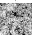
- Figure 1 shows the Scanning electron micrographs of the nanostructure of four representative CNT/P3HT nanocomposites given in Table2 (from top left to bottom right: (a) 30 wt% CNTs, (b) 80 wt% CNTs, (c) 30 wt% acid-treated CNTs, and (d) 60s UV-treated 30 wt% CNTs). Varying amounts of CNT bundles and P3HT matrix are visible in all samples. Additionally, the 80 wt% samples contain Fe-catalyst, and in the UV-treated samples, scrap-like features are visible.
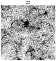
- Figure 2 shows AFM topography of the four representative CNT/P3HT nanocomposites (from top left to bottom right: 30 wt% CNTs, 80 wt% CNTs, 30 wt% acid-treated CNTs, and 60s UV-treated 30 wt% CNTs) shows that 80 wt% and UV-treated samples exhibit considerable roughness.
- Atomic force microscopy (AFM) images reveal an increase in surface roughness with increasing CNT content ( Figure 2 ).
- the resulting films clearly show a fine fibrillar structure with an average bundle diameter of 55 ⁇ 15 nm, which is significantly smaller than for the high CNT content samples ( Figure 1 and 2 ).
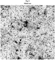
- Figure 3 , 4 and 5 shows Transmission X-ray micrographs measured at 399 eV, 520 eV and 707 eV, respectively.
- the measurements depicted in Figure 3 are slightly above K ⁇ (nitrogen). Darker areas correspond to increased absorption, due to the presence of nitrogen. Darker areas shown in Figure 4 correspond to increased absorption not specific to any element. They are instead indicative of increased sample thickness.
- the measurements depicted in Figure 5 are slightly above L ⁇ (iron). Darker areas correspond to increased absorption caused by iron in the sample.
- TXM transmission X-ray microscopy
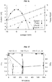
- the dimensionless figure of merit ZT S 2 ⁇ T / ⁇ is typically used, where S is the Seebeck coefficient (S > 0 for p-type and ⁇ 0 for n-type semiconductors), ⁇ the electrical conductivity, ⁇ the thermal conductivity, and T the average absolute temperature.
- the macroscopic ⁇ also increases sharply, in this case by five orders of magnitude, when comparing the neat polymer and composites with weight fractions above percolation.
- the Seebeck coefficient varies from that of the neat polymer ( ⁇ 1000 ⁇ VK -1 ) to that of the CNTs ( ⁇ -10 ⁇ VK -1 ) and correlates well with the percolation threshold observed for ⁇ ( Figure 8b ). Strikingly, at around c s ⁇ 40 wt% CNT content, the Seebeck coefficient changes sign. The corresponding power factor has two regimes, accordingly, separated by a zero value.
- One example consisting of five pairs of such legs is shown in Figure 9 and delivers a thermovoltage of 170 ⁇ VK -1 which is close to the sum of Seebeck coefficients of the constituting legs.
- the Fermi level and the majority charge carrier are then determined by the specific amount of dopants. Furthermore, these composites exhibit thermochromism in solution when heated. Upon increasing the temperature, the composite solution turns from a characteristic dark purple, indicative of ⁇ -stacked/crystalline P3HT, to the bright orange coloration associated with well dissolved (amorphous/isolated) P3HT. Unfortunately, this change is not preserved through the transition to the dried film, as no changes of the thermoelectric properties are observed. Conversely, a reference P3HT solution does not show any changes during preparation and subsequent heating.
- the Seebeck coefficient continuously decreases as a function of irradiation time for the investigated samples, which contain 20 wt% and 30 wt% CNTs ( Figure 10a ).
- S becomes negative after 60s of UV-irradiation.
- thermoelectric properties we next investigate its effect on the structural and optical properties of the composites.
- Optical microscopy indicates that long exposure times ( ⁇ 120 s) yield visibly degraded samples ( Figure 11 ).
- AFM also suggests an increase in surface roughness ( Figure 2 ), while SEM evidences the appearance of small curled scraps ( Figure 1 ), that are electrically insulating ( Figure 6 and 7 ), which we ascribe to degraded polymer.
- Figure 10b shows the normalized absorption and PL intensities of four samples irradiated for 0 s, 60 s, 150 s and 240 s.
- the aforementioned degradation is here seen as an absorption blue-shift, which probably occurs due to a reduction in conjugation length of the polymer.
- the PL quenching that we discussed before is, upon UV irradiation, much less pronounced, demonstrating a lower degree of charge transfer between degraded polymer chains and CNTs, with the concomitant smaller degree of p-doping of the CNTs.
- Figure 10b also shows that there are two clear regimes: for low exposure times ( ⁇ 60 s), there is little degradation of the polymer (no photobleaching, no absorption blue shift, high degree of PL quenching) but a strong change in the electronic properties, as observed by the change in Seebeck sign. Instead, long exposure times (>120 s) result in complete degradation of the polymer with strong negative effects on the electronic properties too.
- the Fourier transform infrared (FTIR) spectra shown in Figure 14 back up this observation, and provide evidence that the UV treatment attacks both the carbon double bonds of the thiophene ring, as well as the alkyl side chains, influencing the doping not only by reducing conjugation, but also by impairing the CNT-P3HT interaction.
- FTIR Fourier transform infrared
- a slight decrease of absorption of these modes is observed with increasing UV treatment time (a, c). This decrease is more pronounced for longer treatment durations (b, c), However an additional effect due to the solvent is then observed.
- thermoelectric module fabricated from a single solution with p- and (UV-irradiated) n-legs was realized.
- Figure 15 illustrates a proof of concept thermoelectric module and some envisaged applications that are implemented through a toroidal geometry of the module.
- FIG. 15 The fabrication is detailed in Figure 15 .
- a uniform wet layer of the composite is deposited on a substrate (s), and part of it is UV-irradiated during drying, resulting in a wet film without treatment (p1) and a wet film that did receive UV treatment (n1).
- the individual legs (p2, n2) of the dried film are patterned by appropriate cutting.
- the device is folded into a spiral, and adjacent couples are connected electrically in series by depositing contacts (c).
- the ends of this spiral are joined to form a torus. Possible applications for this geometry are in the form of a single torus, an extended spiral, and a wristband.
- this module When one side of this module comprising 15 double legs is attached to a glass filled with ice water, leaving the other side at room temperature, it generates a voltage of 5 mV which corresponds to 217.4 ⁇ VK -1 or 14.5 ⁇ V K -1 per couple.
- a plot of the output current and power versus voltage is given in Figure 16 .
- the module supplies ⁇ 2 nA at 5 mV Seebeck voltage.
- An alternative geometry may allow connecting a larger number of legs to harvest, for instance, waste heat from a pipe. For this, the spiral itself can be wound into yet another spiral.
- Figure 17 shows the results of repeated electrical measurements carried out over a period of up to 600 days.
- the conductivity stabilized at 41 % of the initial value, with both high CNT content and UV treated samples following a similar trend.
- the negative Seebeck coefficient of these samples was stable for every single measured n-type sample, with no significant changes observed after 240 days.
- the Seebeck coefficient of p-type samples diminished to 40 % of the initial value and the electrical conductivity to 11 % of of the initial value.
- Table 3 Measured properties used to determine the thermal conductivity ⁇ of bulk P3HT-CNT samples with 13 mm diameter.
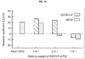
- SG65i CoMoCAT SWCNTs (SouthWest NanoTechnologies) containing ⁇ 40 % (6,5) tubes which are p-type due to doping by atmospheric oxygen, and branched polyethylenimine (PEI, Mw ⁇ 800 g mol -1 , Mw/Mn ⁇ 1.33), an electron-rich polymer, were bought from SigmaAldrich.
- PEI branched polyethylenimine
- CNTs were dispersed in oDCB at a concentration of 0.5 g L -1 and sonicated in ice water for 60 min.
- PEI was added in three steps, followed each time by 30 min sonication.
- the prepared solution was drop-cast onto PET substrates and left to evaporate.
- Fig. 18 shows the measured Seebeck coefficient for samples of different composition, with and without UV-treatment. Concretely, Fig. 18 shows the Seebeck coefficient of composites of single-walled CNTs (which are p-type due to doping with atmospheric oxygen), n-doped with electron-rich PEI.
- n-type samples are obtained for a concentration of PEI greater than 33 wt%.
- the UV-treatment has the opposite effect, increasing the Seebeck coefficient of all studied samples.
Landscapes
- Engineering & Computer Science (AREA)
- Chemical & Material Sciences (AREA)
- Materials Engineering (AREA)
- Nanotechnology (AREA)
- Manufacturing & Machinery (AREA)
- Carbon And Carbon Compounds (AREA)
- Photovoltaic Devices (AREA)
Claims (15)
- Procédé d'obtention d'un semi-conducteur organique de type n à partir d'un semi-conducteur de type p ou d'un semi-conducteur organique de type p à partir d'un semi-conducteur organique de type n comprenant les étapes suivantes :a) préparer un film d'un semi-conducteur organique de type p ou d'un semi-conducteur organique de type n sur un substrat, respectivement,
dans lequel le semi-conducteur organique comprend une nanostructure semi-conductrice et un accepteur ou donneur d'électrons respectivement ; etb) irradier le film obtenu à l'étape (a) par un rayonnement UV-VIS avec une puissance comprise entre 1 mW/cm2 et 100 mW/cm2 caractérisé en ce que le temps d'exposition est compris entre 0,1 s et 600 s et que le processus est effectué en présence d'une atmosphère contenant de l'oxygène. - Procédé d'obtention d'un semi-conducteur organique de type n à partir d'un semi-conducteur de type p selon la revendication 1, caractérisé en ce que le procédé comprend les étapes suivantes :a) préparer un film d'un semi-conducteur organique de type p sur un substrat flexible, ledit substrat souple choisi parmi le polyéthylène téréphtalate, le polyéthylène naphtalate, le polyimide, le polyéthylène, le polystyrène, la chlorure de polyvinyle, le polytétrafluoroéthylène, le polypropylène, le polyuréthane, le polyfluorure de vinylidène et une combinaison de ceux-ci,
dans lequel ledit semi-conducteur organique de type p comprend• une nanostructure semi-conductrice de type n comprise entre 0,1 % et 60 % en poids ; ladite nanostructure semi-conductrice de type n choisie dans la liste consistant en les nanotubes de carbone dopés N, les feuilles de graphène et les nanoplaquettes de graphite dopées N, les nanorubans de graphène dopés N, les fullerènes, les nanofils de silicium dopés au phosphore, les nanofils de tellure tels que les nanofils Bi2Te3 ou les nanofils PbTe, les nanofils à base d'oxyde de zinc, les nanofils à base d'oxyde de titane et une combinaison de ceux-ci, et• une molécule conjuguée semi-conductrice de type p, ladite molécule organique conjuguée semi-conductrice de type p choisie parmi les polyalkylthiophènes, les polyfluorènes, la polyaniline, le polyacétylène, le polyphénylène vinylène, le tétracyanoquinodiméthane, le tétrathiafulvalène et une combinaison de ceux-ci ;et dans lequel ladite nanostructure semi-conductrice de type n est dispersée dans la molécule conjuguée semi-conductrice de type p ; etb) irradier le film obtenu à l'étape (a) par un rayonnement UV-VIS avec une puissance comprise entre 1 mW/cm2 et 100 mW/cm2 et un temps d'exposition compris entre 0,1 s et 600 s et en présence d'une atmosphère contenant de l'oxygène. - Procédé de contrôle selon la revendication 2, dans lequel la molécule organique conjuguée semi-conductrice de type p de l'étape (a) est un poly(3-hexylthiophène), le poly(3-dodécylthiophène-2,5-diyl) ou le poly(9,9-dioctylfluorène).
- Procédé selon l'une quelconque des revendications 2 ou 3, dans lequel la nanostructure semi-conductrice de type n de l'étape (a) est comprise entre 20 % et 40 % en poids.
- Procédé selon l'une quelconque des revendications 2 à 4, dans lequel l'étape a) comprend les étapes suivantes :a1) ajouter une solution de molécule conjuguée semi-conductrice de type p comprenant une molécule conjuguée semi-conductrice de type p et un solvant à une dispersion de nanostructure semi-conductrice de type n comprenant une nanostructure semi-conductrice de type n et un solvant ;a2) agiter le mélange obtenu dans (a1) à une plage de température entre - 20 °C et 200 °C ; eta3) déposer la solution obtenue à l'étape (a2) sur un substrat.
- Procédé de contrôle selon la revendication 5, dans lequel l'étape (a2) est effectuée dans une plage de température comprise entre 0 °C et 100 °C.
- Procédé selon l'une quelconque des revendications 5 ou 6, caractérisé en ce qu'il comprend une étape (a1'), entre l'étape (a1) et l'étape (a2), consistant à ajouter un tensioactif au mélange obtenu à (a1).
- Procédé selon l'une quelconque des revendications 5 à 6, dans lequel le film humide obtenu à l'étape (a3) a une épaisseur comprise entre 10 µm et 1000 µm.
- Procédé de contrôle selon la revendication 8, dans lequel le film humide obtenu à l'étape (a3) a une épaisseur comprise entre 100 µm et 1000 µm.
- Procédé selon l'une quelconque des revendications 1 à 9, dans lequel l'étape a) comprend les étapes suivantes :les étapes (a1) à (a3) selon l'une quelconque des revendications 7 ou 8 ; etune étape (a4) de séchage du film humide obtenu à l'étape (a3) en évaporant les solvants, dans lequel le film séché obtenu à l'étape (a4) a une épaisseur comprise entre 10 nm et 100 µm.
- Procédé de contrôle selon la revendication 10, dans lequel le film séché obtenu à l'étape (a4) a une épaisseur comprise entre 1 µm et 10 µm.
- Procédé d'obtention d'un semi-conducteur organique de type p à partir d'un semi-conducteur organique de type n selon la revendication 1, caractérisé en ce que le procédé comprend les étapes suivantes :a) préparer un film d'un semi-conducteur organique de type n sur un substrat flexible et choisi parmi le polyéthylène téréphtalate, le polyéthylène naphtalate, le polyimide, le polyéthylène, le polystyrène, la chlorure de polyvinyle, le polytétrafluoroéthylène, le polypropylène, le polyuréthane, le polyfluorure de vinylidène et une combinaison de ceux-ci,
dans lequel ledit semi-conducteur organique de type n comprend• une nanostructure semi-conductrice de type p comprise entre 0,1 % et 80 % en poids ; choisi parmi les nanotubes de carbone simple, double, et plusieurs parois, les feuilles de graphène et les nanoplaquettes de graphite, les nanorubans de graphène ; les nanotubes de carbone simple, double et multi-parois dopés au bore, les feuilles de graphène dopées au bore et les nanoplaquettes de graphite dopées au bore, les nanorubans de graphène dopés au bore, les fullerènes dopés au bore et une combinaison de ceux-ci ; et• une molécule riche en électrons choisie parmi la polyéthylèneimine (PEI), le diéthylènetriamine (DETA), l'hydroxyde de tétraméthylammonium (TMAH), le tétrakis(diméthylamino)éthylène (TDAE), le 4-H-benzimidazol-2-yl)-N,N-diméthylbenzénamine (N-DMBI), le 4-HN,N-diphénylaniline (N-DPBI), le triphénylphosphine (tpp), le 1,3-bis(diphénylphosphino)propane (dppp) ;et dans lequel ladite nanostructure semi-conductrice de type p est dispersée dans la molécule riche en électrons ; etb) irradier le film obtenu à l'étape (a) par un rayonnement UV-VIS avec une puissance comprise entre 1 mW/cm2 et 100 mW/cm2 et un temps d'exposition compris entre 0,1 s et 600 s et en présence d'une atmosphère contenant de l'oxygène. - Procédé de contrôle selon la revendication 12, dans lequel la nanostructure semi-conductrice de type p de l'étape (a) se situe dans une plage allant de 40 % à 80 % en poids.
- Procédé selon l'une quelconque des revendications 1 à 13, dans lequel l'étape (b) est réalisée par rayonnement UV-VIS avec une puissance comprise entre 40 mW/cm2 et 60 mW/cm2 et un temps d'exposition compris entre 50 et 100 s.
- Procédé selon l'une quelconque des revendications 1 à 14, dans lequel l'étape (b) est réalisée en utilisant une source laser, une diode ou une lampe.
Applications Claiming Priority (2)
| Application Number | Priority Date | Filing Date | Title |
|---|---|---|---|
| ES201531706A ES2613546B1 (es) | 2015-11-24 | 2015-11-24 | Un procedimiento de obtención de un semiconductor orgánico de tipo n mediante irradiación UV-VIS |
| PCT/EP2016/078459 WO2017089351A1 (fr) | 2015-11-24 | 2016-11-22 | Procédé d'obtention d'un semi-conducteur organique de type n ou de type p par irradiation uv-vis |
Publications (2)
| Publication Number | Publication Date |
|---|---|
| EP3381069A1 EP3381069A1 (fr) | 2018-10-03 |
| EP3381069B1 true EP3381069B1 (fr) | 2019-10-30 |
Family
ID=57485446
Family Applications (1)
| Application Number | Title | Priority Date | Filing Date |
|---|---|---|---|
| EP16805994.7A Not-in-force EP3381069B1 (fr) | 2015-11-24 | 2016-11-22 | Procédé d'obtention d'un semi-conducteur organique de type n ou de type p par irradiation uv-vis |
Country Status (3)
| Country | Link |
|---|---|
| EP (1) | EP3381069B1 (fr) |
| ES (1) | ES2613546B1 (fr) |
| WO (1) | WO2017089351A1 (fr) |
Cited By (1)
| Publication number | Priority date | Publication date | Assignee | Title |
|---|---|---|---|---|
| CN107681043A (zh) * | 2017-09-15 | 2018-02-09 | 武汉理工大学 | 一种柔性热电器件应用的碲化铋基复合热电材料及其制备方法 |
Family Cites Families (2)
| Publication number | Priority date | Publication date | Assignee | Title |
|---|---|---|---|---|
| US20120312343A1 (en) * | 2011-04-12 | 2012-12-13 | Nanocomp Technologies, Inc. | Nanostructured material based thermoelectric generators and methods of generating power |
| HK1219571A1 (zh) * | 2013-03-14 | 2017-04-07 | Wake Forest University | 热电装置和制品及其应用 |
-
2015
- 2015-11-24 ES ES201531706A patent/ES2613546B1/es not_active Expired - Fee Related
-
2016
- 2016-11-22 EP EP16805994.7A patent/EP3381069B1/fr not_active Not-in-force
- 2016-11-22 WO PCT/EP2016/078459 patent/WO2017089351A1/fr not_active Ceased
Non-Patent Citations (1)
| Title |
|---|
| None * |
Cited By (1)
| Publication number | Priority date | Publication date | Assignee | Title |
|---|---|---|---|---|
| CN107681043A (zh) * | 2017-09-15 | 2018-02-09 | 武汉理工大学 | 一种柔性热电器件应用的碲化铋基复合热电材料及其制备方法 |
Also Published As
| Publication number | Publication date |
|---|---|
| EP3381069A1 (fr) | 2018-10-03 |
| WO2017089351A1 (fr) | 2017-06-01 |
| ES2613546A1 (es) | 2017-05-24 |
| ES2613546B1 (es) | 2018-02-28 |
Similar Documents
| Publication | Publication Date | Title |
|---|---|---|
| Liu et al. | Simultaneous enhancement of electrical conductivity and seebeck coefficient in organic thermoelectric SWNT/PEDOT: PSS nanocomposites | |
| Dörling et al. | Photoinduced p-to n-type switching in thermoelectric polymer-carbon nanotube composites | |
| Jung et al. | Efficient debundling of few-walled carbon nanotubes by wrapping with donor–acceptor polymers for improving thermoelectric properties | |
| Schlierf et al. | Graphene–organic composites for electronics: optical and electronic interactions in vacuum, liquids and thin solid films | |
| Salim et al. | Semiconducting carbon nanotubes for improved efficiency and thermal stability of polymer–fullerene solar cells | |
| US10928334B2 (en) | Methods of preparing single-walled carbon nanotube networks | |
| Dörling et al. | Exploring different doping mechanisms in thermoelectric polymer/carbon nanotube composites | |
| Park et al. | Enhancement of the field-effect mobility of poly (3-hexylthiophene)/functionalized carbon nanotube hybrid transistors | |
| US8513804B2 (en) | Nanotube-based electrodes | |
| Hsu et al. | Sorting-free utilization of semiconducting carbon nanotubes for large thermoelectric responses | |
| Abu-Abdeen et al. | Physical characterizations of semi-conducting conjugated polymer-CNTs nanocomposites | |
| Buks et al. | Growth mechanisms and related thermoelectric properties of innovative hybrid networks fabricated by direct deposition of Bi2Se3 and Sb2Te3 on multiwalled carbon nanotubes | |
| Rathore et al. | Influence of MWCNT doping on performance of polymer bulk heterojunction based devices | |
| Delacou et al. | Investigation of charge interaction between fullerene derivatives and single‐walled carbon nanotubes | |
| Liu et al. | Molecular doping of a naphthalene diimide–bithiophene copolymer and SWCNTs for n-type thermoelectric composites | |
| Mardi et al. | Enhanced thermoelectric properties of poly (3-hexylthiophene) through the Incorporation of aligned carbon nanotube forest and chemical treatments | |
| Tonga et al. | Enhanced thermoelectric properties of PEDOT: PSS composites by functionalized single wall carbon nanotubes | |
| Alhashmi Alamer et al. | Manufacturing Organic Environmentally Friendly Electrical Circuits Using the Composites’ Single‐Walled Carbon Nanotubes and PEDOT: PSS | |
| Reyes-Reyes et al. | Bulk heterojunction organic photovoltaic based on polythiophene–polyelectrolyte carbon nanotube composites | |
| Ali et al. | Gas phase doping of pre-fabricated CNT yarns for enhanced thermoelectric properties | |
| Wang et al. | Monodispersed semiconducting SWNTs significantly enhanced the thermoelectric performance of regioregular poly (3-dodecylthiophene) films | |
| EP3381069B1 (fr) | Procédé d'obtention d'un semi-conducteur organique de type n ou de type p par irradiation uv-vis | |
| Chehata et al. | Hybrid nanocomposites based on conducting polymer and silicon nanowires for photovoltaic application | |
| Bakour et al. | Photoexcitations in fully organic nanocomposites of poly (3-hexylthiophene) and multiwalled carbon nanotubes | |
| Horike et al. | Photoinduced charge-carrier modulation of inkjet-printed carbon nanotubes via poly (vinyl acetate) doping and dedoping for thermoelectric generators |
Legal Events
| Date | Code | Title | Description |
|---|---|---|---|
| STAA | Information on the status of an ep patent application or granted ep patent |
Free format text: STATUS: UNKNOWN |
|
| STAA | Information on the status of an ep patent application or granted ep patent |
Free format text: STATUS: THE INTERNATIONAL PUBLICATION HAS BEEN MADE |
|
| PUAI | Public reference made under article 153(3) epc to a published international application that has entered the european phase |
Free format text: ORIGINAL CODE: 0009012 |
|
| STAA | Information on the status of an ep patent application or granted ep patent |
Free format text: STATUS: REQUEST FOR EXAMINATION WAS MADE |
|
| 17P | Request for examination filed |
Effective date: 20180531 |
|
| AK | Designated contracting states |
Kind code of ref document: A1 Designated state(s): AL AT BE BG CH CY CZ DE DK EE ES FI FR GB GR HR HU IE IS IT LI LT LU LV MC MK MT NL NO PL PT RO RS SE SI SK SM TR |
|
| AX | Request for extension of the european patent |
Extension state: BA ME |
|
| STAA | Information on the status of an ep patent application or granted ep patent |
Free format text: STATUS: EXAMINATION IS IN PROGRESS |
|
| DAV | Request for validation of the european patent (deleted) | ||
| DAX | Request for extension of the european patent (deleted) | ||
| 17Q | First examination report despatched |
Effective date: 20190228 |
|
| GRAP | Despatch of communication of intention to grant a patent |
Free format text: ORIGINAL CODE: EPIDOSNIGR1 |
|
| STAA | Information on the status of an ep patent application or granted ep patent |
Free format text: STATUS: GRANT OF PATENT IS INTENDED |
|
| INTG | Intention to grant announced |
Effective date: 20190710 |
|
| GRAS | Grant fee paid |
Free format text: ORIGINAL CODE: EPIDOSNIGR3 |
|
| GRAA | (expected) grant |
Free format text: ORIGINAL CODE: 0009210 |
|
| STAA | Information on the status of an ep patent application or granted ep patent |
Free format text: STATUS: THE PATENT HAS BEEN GRANTED |
|
| AK | Designated contracting states |
Kind code of ref document: B1 Designated state(s): AL AT BE BG CH CY CZ DE DK EE ES FI FR GB GR HR HU IE IS IT LI LT LU LV MC MK MT NL NO PL PT RO RS SE SI SK SM TR |
|
| REG | Reference to a national code |
Ref country code: GB Ref legal event code: FG4D |
|
| REG | Reference to a national code |
Ref country code: CH Ref legal event code: EP |
|
| REG | Reference to a national code |
Ref country code: AT Ref legal event code: REF Ref document number: 1197100 Country of ref document: AT Kind code of ref document: T Effective date: 20191115 |
|
| REG | Reference to a national code |
Ref country code: DE Ref legal event code: R096 Ref document number: 602016023457 Country of ref document: DE |
|
| REG | Reference to a national code |
Ref country code: IE Ref legal event code: FG4D |
|
| REG | Reference to a national code |
Ref country code: LT Ref legal event code: MG4D |
|
| PG25 | Lapsed in a contracting state [announced via postgrant information from national office to epo] |
Ref country code: FI Free format text: LAPSE BECAUSE OF FAILURE TO SUBMIT A TRANSLATION OF THE DESCRIPTION OR TO PAY THE FEE WITHIN THE PRESCRIBED TIME-LIMIT Effective date: 20191030 Ref country code: BG Free format text: LAPSE BECAUSE OF FAILURE TO SUBMIT A TRANSLATION OF THE DESCRIPTION OR TO PAY THE FEE WITHIN THE PRESCRIBED TIME-LIMIT Effective date: 20200130 Ref country code: PT Free format text: LAPSE BECAUSE OF FAILURE TO SUBMIT A TRANSLATION OF THE DESCRIPTION OR TO PAY THE FEE WITHIN THE PRESCRIBED TIME-LIMIT Effective date: 20200302 Ref country code: LV Free format text: LAPSE BECAUSE OF FAILURE TO SUBMIT A TRANSLATION OF THE DESCRIPTION OR TO PAY THE FEE WITHIN THE PRESCRIBED TIME-LIMIT Effective date: 20191030 Ref country code: NL Free format text: LAPSE BECAUSE OF FAILURE TO SUBMIT A TRANSLATION OF THE DESCRIPTION OR TO PAY THE FEE WITHIN THE PRESCRIBED TIME-LIMIT Effective date: 20191030 Ref country code: SE Free format text: LAPSE BECAUSE OF FAILURE TO SUBMIT A TRANSLATION OF THE DESCRIPTION OR TO PAY THE FEE WITHIN THE PRESCRIBED TIME-LIMIT Effective date: 20191030 Ref country code: NO Free format text: LAPSE BECAUSE OF FAILURE TO SUBMIT A TRANSLATION OF THE DESCRIPTION OR TO PAY THE FEE WITHIN THE PRESCRIBED TIME-LIMIT Effective date: 20200130 Ref country code: LT Free format text: LAPSE BECAUSE OF FAILURE TO SUBMIT A TRANSLATION OF THE DESCRIPTION OR TO PAY THE FEE WITHIN THE PRESCRIBED TIME-LIMIT Effective date: 20191030 Ref country code: GR Free format text: LAPSE BECAUSE OF FAILURE TO SUBMIT A TRANSLATION OF THE DESCRIPTION OR TO PAY THE FEE WITHIN THE PRESCRIBED TIME-LIMIT Effective date: 20200131 Ref country code: PL Free format text: LAPSE BECAUSE OF FAILURE TO SUBMIT A TRANSLATION OF THE DESCRIPTION OR TO PAY THE FEE WITHIN THE PRESCRIBED TIME-LIMIT Effective date: 20191030 |
|
| REG | Reference to a national code |
Ref country code: NL Ref legal event code: MP Effective date: 20191030 |
|
| PG25 | Lapsed in a contracting state [announced via postgrant information from national office to epo] |
Ref country code: RS Free format text: LAPSE BECAUSE OF FAILURE TO SUBMIT A TRANSLATION OF THE DESCRIPTION OR TO PAY THE FEE WITHIN THE PRESCRIBED TIME-LIMIT Effective date: 20191030 Ref country code: HR Free format text: LAPSE BECAUSE OF FAILURE TO SUBMIT A TRANSLATION OF THE DESCRIPTION OR TO PAY THE FEE WITHIN THE PRESCRIBED TIME-LIMIT Effective date: 20191030 Ref country code: IS Free format text: LAPSE BECAUSE OF FAILURE TO SUBMIT A TRANSLATION OF THE DESCRIPTION OR TO PAY THE FEE WITHIN THE PRESCRIBED TIME-LIMIT Effective date: 20200229 |
|
| PG25 | Lapsed in a contracting state [announced via postgrant information from national office to epo] |
Ref country code: AL Free format text: LAPSE BECAUSE OF FAILURE TO SUBMIT A TRANSLATION OF THE DESCRIPTION OR TO PAY THE FEE WITHIN THE PRESCRIBED TIME-LIMIT Effective date: 20191030 |
|
| REG | Reference to a national code |
Ref country code: CH Ref legal event code: PL |
|
| PG25 | Lapsed in a contracting state [announced via postgrant information from national office to epo] |
Ref country code: LI Free format text: LAPSE BECAUSE OF NON-PAYMENT OF DUE FEES Effective date: 20191130 Ref country code: DK Free format text: LAPSE BECAUSE OF FAILURE TO SUBMIT A TRANSLATION OF THE DESCRIPTION OR TO PAY THE FEE WITHIN THE PRESCRIBED TIME-LIMIT Effective date: 20191030 Ref country code: MC Free format text: LAPSE BECAUSE OF FAILURE TO SUBMIT A TRANSLATION OF THE DESCRIPTION OR TO PAY THE FEE WITHIN THE PRESCRIBED TIME-LIMIT Effective date: 20191030 Ref country code: EE Free format text: LAPSE BECAUSE OF FAILURE TO SUBMIT A TRANSLATION OF THE DESCRIPTION OR TO PAY THE FEE WITHIN THE PRESCRIBED TIME-LIMIT Effective date: 20191030 Ref country code: ES Free format text: LAPSE BECAUSE OF FAILURE TO SUBMIT A TRANSLATION OF THE DESCRIPTION OR TO PAY THE FEE WITHIN THE PRESCRIBED TIME-LIMIT Effective date: 20191030 Ref country code: CZ Free format text: LAPSE BECAUSE OF FAILURE TO SUBMIT A TRANSLATION OF THE DESCRIPTION OR TO PAY THE FEE WITHIN THE PRESCRIBED TIME-LIMIT Effective date: 20191030 Ref country code: RO Free format text: LAPSE BECAUSE OF FAILURE TO SUBMIT A TRANSLATION OF THE DESCRIPTION OR TO PAY THE FEE WITHIN THE PRESCRIBED TIME-LIMIT Effective date: 20191030 Ref country code: LU Free format text: LAPSE BECAUSE OF NON-PAYMENT OF DUE FEES Effective date: 20191122 Ref country code: CH Free format text: LAPSE BECAUSE OF NON-PAYMENT OF DUE FEES Effective date: 20191130 |
|
| REG | Reference to a national code |
Ref country code: DE Ref legal event code: R097 Ref document number: 602016023457 Country of ref document: DE |
|
| REG | Reference to a national code |
Ref country code: AT Ref legal event code: MK05 Ref document number: 1197100 Country of ref document: AT Kind code of ref document: T Effective date: 20191030 |
|
| REG | Reference to a national code |
Ref country code: BE Ref legal event code: MM Effective date: 20191130 |
|
| PG25 | Lapsed in a contracting state [announced via postgrant information from national office to epo] |
Ref country code: SK Free format text: LAPSE BECAUSE OF FAILURE TO SUBMIT A TRANSLATION OF THE DESCRIPTION OR TO PAY THE FEE WITHIN THE PRESCRIBED TIME-LIMIT Effective date: 20191030 Ref country code: IT Free format text: LAPSE BECAUSE OF FAILURE TO SUBMIT A TRANSLATION OF THE DESCRIPTION OR TO PAY THE FEE WITHIN THE PRESCRIBED TIME-LIMIT Effective date: 20191030 Ref country code: SM Free format text: LAPSE BECAUSE OF FAILURE TO SUBMIT A TRANSLATION OF THE DESCRIPTION OR TO PAY THE FEE WITHIN THE PRESCRIBED TIME-LIMIT Effective date: 20191030 |
|
| PLBE | No opposition filed within time limit |
Free format text: ORIGINAL CODE: 0009261 |
|
| STAA | Information on the status of an ep patent application or granted ep patent |
Free format text: STATUS: NO OPPOSITION FILED WITHIN TIME LIMIT |
|
| 26N | No opposition filed |
Effective date: 20200731 |
|
| PG25 | Lapsed in a contracting state [announced via postgrant information from national office to epo] |
Ref country code: IE Free format text: LAPSE BECAUSE OF NON-PAYMENT OF DUE FEES Effective date: 20191122 |
|
| PG25 | Lapsed in a contracting state [announced via postgrant information from national office to epo] |
Ref country code: AT Free format text: LAPSE BECAUSE OF FAILURE TO SUBMIT A TRANSLATION OF THE DESCRIPTION OR TO PAY THE FEE WITHIN THE PRESCRIBED TIME-LIMIT Effective date: 20191030 Ref country code: SI Free format text: LAPSE BECAUSE OF FAILURE TO SUBMIT A TRANSLATION OF THE DESCRIPTION OR TO PAY THE FEE WITHIN THE PRESCRIBED TIME-LIMIT Effective date: 20191030 Ref country code: BE Free format text: LAPSE BECAUSE OF NON-PAYMENT OF DUE FEES Effective date: 20191130 |
|
| PG25 | Lapsed in a contracting state [announced via postgrant information from national office to epo] |
Ref country code: CY Free format text: LAPSE BECAUSE OF FAILURE TO SUBMIT A TRANSLATION OF THE DESCRIPTION OR TO PAY THE FEE WITHIN THE PRESCRIBED TIME-LIMIT Effective date: 20191030 |
|
| GBPC | Gb: european patent ceased through non-payment of renewal fee |
Effective date: 20201122 |
|
| PG25 | Lapsed in a contracting state [announced via postgrant information from national office to epo] |
Ref country code: MT Free format text: LAPSE BECAUSE OF FAILURE TO SUBMIT A TRANSLATION OF THE DESCRIPTION OR TO PAY THE FEE WITHIN THE PRESCRIBED TIME-LIMIT Effective date: 20191030 Ref country code: HU Free format text: LAPSE BECAUSE OF FAILURE TO SUBMIT A TRANSLATION OF THE DESCRIPTION OR TO PAY THE FEE WITHIN THE PRESCRIBED TIME-LIMIT; INVALID AB INITIO Effective date: 20161122 |
|
| PG25 | Lapsed in a contracting state [announced via postgrant information from national office to epo] |
Ref country code: GB Free format text: LAPSE BECAUSE OF NON-PAYMENT OF DUE FEES Effective date: 20201122 |
|
| PGFP | Annual fee paid to national office [announced via postgrant information from national office to epo] |
Ref country code: DE Payment date: 20211126 Year of fee payment: 6 Ref country code: FR Payment date: 20211124 Year of fee payment: 6 |
|
| PG25 | Lapsed in a contracting state [announced via postgrant information from national office to epo] |
Ref country code: TR Free format text: LAPSE BECAUSE OF FAILURE TO SUBMIT A TRANSLATION OF THE DESCRIPTION OR TO PAY THE FEE WITHIN THE PRESCRIBED TIME-LIMIT Effective date: 20191030 |
|
| PG25 | Lapsed in a contracting state [announced via postgrant information from national office to epo] |
Ref country code: MK Free format text: LAPSE BECAUSE OF FAILURE TO SUBMIT A TRANSLATION OF THE DESCRIPTION OR TO PAY THE FEE WITHIN THE PRESCRIBED TIME-LIMIT Effective date: 20191030 |
|
| REG | Reference to a national code |
Ref country code: DE Ref legal event code: R079 Ref document number: 602016023457 Country of ref document: DE Free format text: PREVIOUS MAIN CLASS: H01L0051000000 Ipc: H10K0099000000 |
|
| REG | Reference to a national code |
Ref country code: DE Ref legal event code: R119 Ref document number: 602016023457 Country of ref document: DE |
|
| PG25 | Lapsed in a contracting state [announced via postgrant information from national office to epo] |
Ref country code: DE Free format text: LAPSE BECAUSE OF NON-PAYMENT OF DUE FEES Effective date: 20230601 |
|
| PG25 | Lapsed in a contracting state [announced via postgrant information from national office to epo] |
Ref country code: FR Free format text: LAPSE BECAUSE OF NON-PAYMENT OF DUE FEES Effective date: 20221130 |