EP3381066B1 - A memristor device and a method of fabrication thereof - Google Patents
A memristor device and a method of fabrication thereof Download PDFInfo
- Publication number
- EP3381066B1 EP3381066B1 EP16867449.7A EP16867449A EP3381066B1 EP 3381066 B1 EP3381066 B1 EP 3381066B1 EP 16867449 A EP16867449 A EP 16867449A EP 3381066 B1 EP3381066 B1 EP 3381066B1
- Authority
- EP
- European Patent Office
- Prior art keywords
- layer
- metal oxide
- switching
- amorphous metal
- memristor device
- Prior art date
- Legal status (The legal status is an assumption and is not a legal conclusion. Google has not performed a legal analysis and makes no representation as to the accuracy of the status listed.)
- Active
Links
Images

Classifications
-
- H—ELECTRICITY
- H10—SEMICONDUCTOR DEVICES; ELECTRIC SOLID-STATE DEVICES NOT OTHERWISE PROVIDED FOR
- H10N—ELECTRIC SOLID-STATE DEVICES NOT OTHERWISE PROVIDED FOR
- H10N70/00—Solid-state devices having no potential barriers, and specially adapted for rectifying, amplifying, oscillating or switching
- H10N70/801—Constructional details of multistable switching devices
- H10N70/881—Switching materials
- H10N70/883—Oxides or nitrides
- H10N70/8836—Complex metal oxides, e.g. perovskites, spinels
-
- H—ELECTRICITY
- H10—SEMICONDUCTOR DEVICES; ELECTRIC SOLID-STATE DEVICES NOT OTHERWISE PROVIDED FOR
- H10N—ELECTRIC SOLID-STATE DEVICES NOT OTHERWISE PROVIDED FOR
- H10N70/00—Solid-state devices having no potential barriers, and specially adapted for rectifying, amplifying, oscillating or switching
- H10N70/20—Multistable switching devices, e.g. memristors
- H10N70/24—Multistable switching devices, e.g. memristors based on migration or redistribution of ionic species, e.g. anions, vacancies
-
- H—ELECTRICITY
- H10—SEMICONDUCTOR DEVICES; ELECTRIC SOLID-STATE DEVICES NOT OTHERWISE PROVIDED FOR
- H10N—ELECTRIC SOLID-STATE DEVICES NOT OTHERWISE PROVIDED FOR
- H10N70/00—Solid-state devices having no potential barriers, and specially adapted for rectifying, amplifying, oscillating or switching
- H10N70/011—Manufacture or treatment of multistable switching devices
- H10N70/021—Formation of switching materials, e.g. deposition of layers
-
- H—ELECTRICITY
- H10—SEMICONDUCTOR DEVICES; ELECTRIC SOLID-STATE DEVICES NOT OTHERWISE PROVIDED FOR
- H10N—ELECTRIC SOLID-STATE DEVICES NOT OTHERWISE PROVIDED FOR
- H10N70/00—Solid-state devices having no potential barriers, and specially adapted for rectifying, amplifying, oscillating or switching
- H10N70/011—Manufacture or treatment of multistable switching devices
- H10N70/021—Formation of switching materials, e.g. deposition of layers
- H10N70/026—Formation of switching materials, e.g. deposition of layers by physical vapor deposition, e.g. sputtering
-
- H—ELECTRICITY
- H10—SEMICONDUCTOR DEVICES; ELECTRIC SOLID-STATE DEVICES NOT OTHERWISE PROVIDED FOR
- H10N—ELECTRIC SOLID-STATE DEVICES NOT OTHERWISE PROVIDED FOR
- H10N70/00—Solid-state devices having no potential barriers, and specially adapted for rectifying, amplifying, oscillating or switching
- H10N70/801—Constructional details of multistable switching devices
- H10N70/821—Device geometry
- H10N70/826—Device geometry adapted for essentially vertical current flow, e.g. sandwich or pillar type devices
-
- H—ELECTRICITY
- H10—SEMICONDUCTOR DEVICES; ELECTRIC SOLID-STATE DEVICES NOT OTHERWISE PROVIDED FOR
- H10N—ELECTRIC SOLID-STATE DEVICES NOT OTHERWISE PROVIDED FOR
- H10N70/00—Solid-state devices having no potential barriers, and specially adapted for rectifying, amplifying, oscillating or switching
- H10N70/801—Constructional details of multistable switching devices
- H10N70/841—Electrodes
-
- H—ELECTRICITY
- H10—SEMICONDUCTOR DEVICES; ELECTRIC SOLID-STATE DEVICES NOT OTHERWISE PROVIDED FOR
- H10N—ELECTRIC SOLID-STATE DEVICES NOT OTHERWISE PROVIDED FOR
- H10N70/00—Solid-state devices having no potential barriers, and specially adapted for rectifying, amplifying, oscillating or switching
- H10N70/801—Constructional details of multistable switching devices
- H10N70/881—Switching materials
- H10N70/883—Oxides or nitrides
Definitions
- the present invention relates to a memristor device and a method of fabrication thereof.
- Nanoscale resistive memories (or “memristors”) satisfy many of these requirements, and are reliant on functional oxides. They are normally configured as passive two terminal metal insulated metal (MIM) devices based on functional binary and ternary metal oxides (e.g. TiO 2 , SrTiO 3 ). These offer a scalable, fast, non-volatile and low energy memristive performance. Their dynamic nonlinear current voltage characteristics also suggest applications in nonlinear circuit design and alternative logic architectures.
- MIM passive two terminal metal insulated metal
- bipolar resistive switching behaviour in these devices is treated to a combination of electronic effects at the metal/oxide interfaces and reversible redox reactions and nanoionic transport in transition metal oxide layers. These processes are triggered in the oxide upon the creation of extended defect structures during an electroforming process, under high electrical gradients.
- MIM metal insulated metal
- strontium titanate (SirTiO 3 ; STO), the archetypal perovskite oxide has emerged as a promising candidate for the functional oxide layer in memristive MIM devices. Its self-doping tendency with oxygen vacancies subject to electrical or thermal stress can transform its electronic structure from a band insulator to a metallic conductor and facilitate electroresistive switching suitable for two-terminal memory devices.
- Strontium titanate has shown great potential for nanoscale resistive switching applications due to the inherent tendency of the stable perovskite structure of STO to harbour oxygen vacancy point defects and a pronounced redox activity along the dislocations in the titanium oxide sub-lattice.
- the resistive switching in STO based devices is generally attributed to highly localised accumulation of oxygen vacancies (i.e. nanofilaments) along the extended defect structures, which result in the local bypassing of the depletion layer at the metal-oxide interfaces.
- the defect structure of STO can be directly manipulated via doping with a donor- or acceptor-type transition metal, which can be employed to modulate the electronic structure at local (e.g. grain boundaries and point defects) and bulk levels. This can be used as a tool to engineer the arrangement and electronic/ionic transport properties of nanofilaments, and therefore, the memristive properties of STO-based devices.
- STO-based devices have the potential for high density integration as passive analog memory elements in computing architectures.
- the tunability of the STO structure with respect to coupled electromechanical and electro-optical effects highlights the impressive degree of freedom it can render in the design of multifunctional nonlinear devices.
- the present invention seeks to provide a memristor device and a method of fabrication thereof, which may overcome or substantially ameliorate at least some of the deficiencies of the prior art, or to at least provide an alternative.
- Hussein Nili ET AL “Nanoscale Resistive Switching in Amorphous Perovskite Oxide (a-SrTiO 3) Memristors", Advanced Functional Materials, vol. 24, no. 43, 1 November 2014 (2014-11-01), pages 6741-6750, XP55386480, DE, ISSN: 1616-301X, DOI: 10.1002/adfm.201401278 is directed to synthesizing amorphous STO (a-STO) thin films with controllable as-grown oxygen deficiency induced defect structures at room temperatures having improved resistive switching performances.
- a-STO amorphous STO
- Husssein discusses the electroforming mechanism to facilitate electroresistive switching in intrinsically insulating metal oxides by permanently altering their stoichiometry and oxygen vacancy distribution by way of redox processes.
- the electroforming mechanism is followed by nanoionics switching.
- Hussein Nili ET AL "Donor-Induced Performance Tuning of Amorphous SrTiO 3 Memristive Nanodevices: Multistate Resistive Switching and Mechanical Tunability", Advanced Functional Materials, vol. 25, no. 21, 14 April 2015 (2015-04-14), pages 3172-3182, XP55223949, DE, ISSN: 1616-301X, DOI: 10.1002/adfm.201501019 is directed to dynamics and temperature dependence of memristor performance of a-STO-based devices and focuses on as-grown oxygen vacancy network and donor-induced dislocation sites.
- Hussein describes improvement in stability and controllability of memristor performance due to donor doping in a a-STO network In the article by X.B.
- a memristor device comprising:
- the at least one layer of amorphous metal oxide includes an oxide of titanium.
- the at least one layer of amorphous metal oxide further comprises an amorphous metal oxide layer.
- the amorphous metal oxide layer includes a strontium titanate expressed by a formula (amorphous -SrTiO 3 ).
- each of the oxygen deficient amorphous metal oxide layer and the amorphous metal oxide layer has a thickness that falls within the range of 15 nm to 40 nm.
- the oxygen deficient amorphous metal oxide comprises doping atoms of a dopant element selected from the group consisting of chromium and niobium.
- the dopant element is niobium.
- the ratio of niobium to titanium is between 0.02 and 0.05.
- the least one layer of an amorphous metal oxide has a thickness that falls within the range of 15 nm to 40 nm.
- the cathode metal layer has a thickness that falls within the range of 2 nm to 15 nm.
- the cathode metal layer has a thickness that falls within the range of 5 nm to 10 nm.
- each of the first and second electrodes has a thickness that falls within the range of 25 nm to 35 nm.
- the resistive switching behaviour comprises a bipolar resistive switching behaviour that occurs in one or both of a forward direction and a reverse direction.
- the resistive switching behaviour comprises a bipolar resistive switching behaviour that occurs in one or more of a forward direction, a reverse direction, and a complementary resistive switching behaviour.
- a memristor device comprising the steps of:
- steps a) to d) is conducted at room temperature.
- a memristor device comprising the steps of:
- steps a) to d) is conducted at room temperature.
- the single layer device 10 is a stacked passive to terminal metal insulated metal (MIM) device or cell that comprises first and second electrodes 20, 30 that act as the top and bottom electrodes, respectively, of the single layer MIM device 10.
- the first and second electrodes 20, 30 are inert high work function metal electrodes that are produced from a metal selected from the group consisting of platinum, palladium, gold, tungsten and titanium nitride.
- the first and second electrodes 20, 30 are formed from platinum metal, each having a thickness that falls within the range of 25 nm to 35 nm.
- the first or top platinum electrode 20 has a cathode metal layer 40 disposed on an inwardly facing surface thereof.
- the cathode metal layer 40 is ideally a reactive low work function metal selected from the group consisting of platinum, palladium, gold, palladium-silver, ruthenium and iridium.
- the cathode metal layer 40 is formed from titanium metal having a thickness that falls within the range of 2 nm to 15 nm, more preferably, a thickness that falls within the range of 5 nm to 10 nm.
- an active region Disposed substantially between, and in electrical contact with, the second or bottom platinum electrode 30 and the titanium cathode layer 40 is an active region that comprises a switching layer in the form of an amorphous metal oxide 50.
- the amorphous metal oxide switching layer 50 takes the form of a near stoichiometric, oxygen-deficient amorphous perovskite ternary metal oxide layer of strontium titanate expressed by the formula amorphous-SrTiO 3-x (hereinafter referred to as a -SrTiO 3-x ), wherein 0.05 ⁇ x ⁇ 0.15 (hereinafter, referred to in the shortened notational form as a -STO x ).
- the oxygen-deficient a -STO x switching layer 50 has a thickness that falls within the range of 15 nm to 40 nm, more preferably, within the range of 15 nm to 30 nm, still more preferably, within the range of 15 nm to 25 nm.
- the inventors have found that a desirable requirement for achieving a versatile resistive switching single layer MIM device 10 is low or no initial electrical stress (or electroforming voltage/current) to induce the metal-insulator transition in the single layer MIM device 10.
- three fabrication parameters may be employed to control the electroforming voltage/current threshold in the single layer MIM device 10 of the preferred embodiments of the present invention.
- Control of the oxygen deficiency content in a-STO oxide switching layer is RF magnetron sputtering in an Ar/O 2 sputtering gas mixture using a stoichiometric SrTiO 3 ceramic target.
- the oxygen content in the deposited a-STO switching layer 50 can be controlled.
- the inventors have found that high oxygen deficiency content in the a -STO x switching layer 50 of a single layer MIM device 10 facilitates lower energy requirements for initial electroforming.
- Figure 3(a) shows a chart illustrating the dependence of the rate of oxygen vacancy concentration vs. oxygen pressure for oxygen-deficient a -STO x switching layers 50 deposited on a Si/SiO 2 substrate by RF magnetron sputtering at room temperature.
- Control of oxide thickness / density sputtering power, duration and target to substrate distance can be employed to control the oxide layer thickness and density during the RF sputtering deposition.
- a moderate RF power (100W) and a large target to substrate distance (50 cm) in a "sputter-up" configuration the thickness of the oxide layers can be controlled uniformly down to ⁇ 5 nm.
- the oxygen-deficient a- STO x switching layer 50 used in the single layer MIM device 10 may be varied in thickness between 10 and 40 nm and preferably between 15 and 40 nm to optimize the resistive switching performance of the resulting single layer MIM device 10.
- Figure 3(b) shows a chart illustrating the dependence of the rate of growth of oxygen-deficient a -STO x switching layers 50 vs. plasma discharge power at 0% oxygen partial pressure.
- the above approach allows precise control over the thickness of the oxygen-deficient a -STO x switching layer 50 and the oxygen deficiency concentration.
- the inventors have found that multi-layered or stacked films can be deposited on the substrate with ease. Since the deposition occurs at room temperature, inter-diffusion between the as-grown amorphous oxygen-deficient a -STO x switching layer 50 with defect vacancy profiles is unlikely, and in a worst case scenario, limited to 2-3 nm. Thus the electrical transport properties of each individual layer can be employed to optimize the overall stack's performance.
- Thickness of the cathode metal the thickness of the titanium cathode layer 40 in the single layer MIM device 10 influences the initial resistance and electrical characteristics of the single layer MIM device 10. At a critical thickness, the designed asymmetry in the single layer MIM device 10 allows for robust resistive switching at lower energies.
- a bottom platinum electrode 30 of 25 nm thickness is deposited onto a pre-patterned SiO 2 /Si substrate by electron beam evaporation at room temperature. Adhesion between the pre-patterned SiO 2 /Si substrate and the bottom platinum electrode 30 may be enhanced by virtue of depositing an adhesion promoting layer of TiO 2 of thickness 5 nm onto the pre-patterned SiO 2 /Si substrate prior to applying the bottom platinum electrode 30.
- step 2) an oxygen-deficient a -STO x switching layer 50 of 30 nm thickness is sputtered through a shadow mask onto the bottom platinum electrode 30 by RF magnetron sputtering at room temperature in an Ar/O 2 sputtering gas mixture using a stoichiometric SrTiO 3 ceramic target at a base pressure of ⁇ 10 -7 Torr.
- a preferred partial pressure range to attain single phase perovskite oxide layers is 0-5%, whereupon a 5% oxygen partial pressure yields stoichiometric a-STO thin films and 0% partial pressure yields a maximum oxygen deficiency content of 3-4% in the oxide switching layer 50.
- a titanium cathode layer 40 of thickness 5 nm is first deposited onto the sputtered oxygen-deficient a -STO x switching layer 50 by electron beam evaporation at room temperature.
- a top platinum electrode 20 of thickness 25 nm is deposited onto the titanium cathode layer 40 using the same electron beam evaporation apparatus, again at room temperature.
- the fabrication method described above is not limited to depositing the individual layers by sputtering, but that other deposition methods including thermal evaporation, electron beam evaporation, atomic layer deposition, co-deposition, chemical vapour deposition, ion beam assisted deposition, may also be employed.
- the inventors have found that by virtue of the titanium cathode layer 40 being located between, and in electrical contact with, the top platinum metal electrode 20 and the oxygen-deficient a -STO x switching layer 50, the resulting asymmetry within the single layer MIM device 10 enables a high-performance non-linear resistive switching to be achieved.
- the thickness of the oxygen-deficient a -STO x switching layer 50 and the titanium cathode layer 40 in the single layer MIM device 10 have been optimized to enable low voltage bipolar resistive switching behaviour.
- a single layer MIM device 10 that comprises first and second platinum electrodes 20, 30, each having a thickness of 20 nm, a titanium cathode layer 40 having a thickness, L T , of 5 nm and an oxygen-deficient a -STO x layer 50 having a thickness, L 1 , of 30 nm.
- the inventors have also found that when a switching voltage is applied between the first and second platinum electrodes 20, 30 of the single layer MIM device 10, the oxygen-deficient a -STO x switching layer 50 exhibits a bipolar resistive switching behaviour that occurs in one or both of a forward direction and a reverse direction.
- Figure 1(b) shows a chart illustrating a current-voltage relationship of a single layer a -STO x based MIM device 10 having the above stated dimensions when a bias voltage is applied between the first and second electrodes 20, 30 of the single layer MIM device 10.
- the single layer MIM device 10 persists in the OFF state. However, when a bias voltage is applied to the single layer MIM device 10 from about 0 V to about -1.5 V, biased from the top platinum electrode 20, the single layer MIM device 10 experiences a path of high resistance (path 1) until the current reaches about -5 ⁇ A at a voltage of about -1 V. At this point, the single layer MIM device 10 switches to the ON state, where the current increases to about -330 ⁇ A until the voltage reaches - 1.5 V, corresponding to a low resistance state.
- the inventors have found that the average OFF/ON switching ratio for the single layer MIM device 10 is in the range of 10 2 to 10 3 .
- the bipolar switching behaviour of transition metal oxide layers in a stacked MIM device is generally perceived to be originating from inhomogeneous conduction mechanisms through localized filamentary pathways.
- the single layer MIM device 10 by virtue of the controlled defect-rich structure of the a -STO x switching layer 50 resulting from the oxygen-deficiency, this allows a conductive filamentary pathway (not shown) to be formed between the bottom platinum electrode 30 and the titanium cathode layer 40 of the single layer MIM device 10 when a sufficiently high bias voltage is applied between the first and second platinum electrodes 20, 30. Once the conductive filament pathway has been formed, it may be reset or set by a suitable voltage applied across the structure of the single layer MIM device 10 to provide desirable memristive properties.
- FIG. 2(a) there is provided a schematic cross-sectional view of a representative bilayer layer memristor device 100 produced according to another preferred embodiment of the present invention.
- the bilayer MIM device 100 as shown in Figure 2(a) comprises the same or similar components that make up the single layer MIM device 10 described above, albeit with an additional amorphous metal oxide layer 60 of strontium titanate, expressed by the formula a -SrTiO 3 (hereinafter, referred to in the shortened notational form as a -STO), disposed substantially between the titanium cathode layer 40 and the oxygen-deficient a -STO x switching layer 50.
- a -STO amorphous metal oxide layer 60 of strontium titanate
- the fabrication of the bilayer MIM device 100 involves the additional step, step 3a) , of depositing the a-STO switching layer 60 onto the oxygen-deficient a -STO x switching layer 50 by sputtering through a shadow mask using RF magnetron sputtering at room temperature in an Ar/O 2 sputtering gas mixture using a stoichiometric SrTiO 3 ceramic target at a base pressure of ⁇ 10 -7 Torr.
- titanium cathode layer 40 in the bilayer MIM device 100 performs according to the same or similar principles as in the single layer MIM device 10.
- each of the oxygen deficient a -STO x switching layer 50 and the a-STO switching layer 60 of the bilayer MIM device 100 has a thickness that falls within the range of 15 nm to 40 nm, more preferably, within the range of 15 nm to 30 nm, still more preferably, within the range of 15 nm to 25 nm.
- bilayer MIM device 100 that comprises first and second platinum electrodes 20, 30, each having a thickness of 20 nm, a titanium cathode layer 40 having a thickness, L T , of 5 nm, an a-STO switching layer 60 having a thickness, L 2 , of 20 nm and an oxygen-deficient a -STO x switching layer 50 having a thickness, L 1 , of 20 nm.
- FIG. 2(b) there is shown a chart illustrating a current-voltage relationship of a bilayer MIM device 100 having the above stated dimensions when a bias voltage is applied between the first and second platinum electrodes 20, 30 of the bilayer MIM device 100.
- the bilayer MIM device 100 persists in the OFF state. However, when a bias voltage is applied to the bilayer MIM device 100 from about 0 V to about -3 V, biased from the top platinum electrode 20, the bilayer MIM device 100 experiences a path of high resistance (path 1) until the current reaches a limit of about -5 ⁇ A at a voltage of about -1.8 V. At this point, the bilayer MIM device 100 switches to the ON state, where the current increases to about -70 ⁇ A until the voltage reaches -2.5 V corresponding to a low resistance state.
- the bilayer MIM device 100 When a voltage is subsequently applied from about 0 V to about +4 V, the current starts to decrease and the bilayer MIM device 100 experiences a path of low resistance (along path 2). As the current and voltage pass through the origin and along path 3, the current increases to about +85 ⁇ A at a voltage of about +3.8 V. At this point, the bilayer MIM device 100 switches to the OFF state. When the bias voltage is reduced to about -0 V, the OFF state is maintained as the current falls back to zero as the bilayer MIM device 100 experiences a path of high resistance (path 4). Application of a bias voltage in the low voltage ranges before reaching switching thresholds may not disturb the switching state so that the device may be stable for READ operations.
- the introduction of the additional a-STO switching layer 60 further limits the overall conduction in the bilayer MIM device 100 in either switching regimes (low or high resistance) while keeping the bilayer MIM device 100 forming free. This may allow for resistive switching operation with lower energy requirements.
- the inventors have found that by varying the thicknesses of each of the individual layers of the bilayer MIM device 100 it is possible to fine tune the memristive properties. Indeed, the inventors have found that switching ratios of up to 10 3 are achievable in the bilayer MIM device 100.
- bilayer MIM device 100 Another aspect of the bilayer MIM device 100 is the potential for achieving complementary resistive switching and reversal of the switching polarity.
- V NTH1 indicates the start of a first or ON state switching region and V PTH1 indicates the start of a second or OFF state switching region (or vice versa).
- V NTH2 indicates the end of the first or ON state switching region and V PTH1 indicates the end of the second or OFF state switching region (or vice versa).
- FIG. 2(d) there is shown a chart illustrating a current-voltage relationship of a bilayer layer MIM device 100 having the above stated dimensions when a bias voltage is applied between the first and second platinum electrodes 20, 30 of the bilayer MIM device 100 (biased from the top platinum electrode 30).
- the reversal may be achieved by applying a bias in the positive polarity equal to V PTH1 or in negative polarity equal to V NTH1 .
- These two thresholds may be used to reverse the switching polarity from Figure 2(b) to Figure 2(d) and vice versa.
- the bilayer MIM device 100 persists in the OFF state. However, when a bias voltage is applied to the bilayer MIM device 100 from about 0 V to about +3 V, biased from the bottom platinum electrode 20, the bilayer MIM device 100 experiences a path of high resistance (path 1) until a voltage of about +1.7 V. At this point, the bilayer MIM device 100 switches to the ON state, where the current starts to increase until the voltage reaches +2.2 V resulting in a current of about +50 ⁇ A corresponding to a low resistance state.
- the bilayer MIM device 100 switches from a low resistance state to a high resistance state.
- a voltage is applied in a negative polarity, again biased from the top platinum electrode 30, the bilayer MIM device 100 switches from a high resistance state to a low resistance state.
- This bipolar resistive switching behaviour is performed repeatedly in the same manner, corresponding to a stable non-volatile bipolar switching characteristic, as indicated by the hysteresis resulting from the cycle of operation.
- Application of a bias voltage in the low voltage ranges before reaching switching thresholds may not disturb the switching state so that the device may be stable for READ operations.
- the inventors have found that the same behaviour can be used to utilize the bilayer MIM device 100 for switching in opposite polarities.
- the inventors perceive that the complementary resistive switching (CRS) behaviour observed in the bilayer MIM device 100 involves a reversal in the charge distribution and polarity of the a-STO switching layer 60 and the oxygen-deficient a -STO x switching layer 50, which infers that when one of the two oxide switching layers of the bilayer MIM device 100 is switched ON, the current flow causes the other oxide switching layer to switch OFF.
- CRS complementary resistive switching
- the single layer MIM device 10 and the bilayer MIM device 100 fabricated according to the method of the present invention provide a number of distinct advantages over conventional STO-based memristor devices.
- the single layer and bilayer MIM devices 10, 100 can be fabricated at room temperature and without requiring post-annealing steps, thereby doing away with the high processing temperatures associated with conventional approaches to fabricating STO-based memristor devices.
- the single layer and bilayer MIM devices 10, 100 described above may be fabricated through complementary metal-oxide semiconductor (CMOS) compatible processes on conventional Si and SiO 2 substrates.
- CMOS complementary metal-oxide semiconductor
- the bilayer MIM device 100 can be operated in three distinct modes: (i) forward bipolar resistive switching behaviour (ii) reverse bipolar resistive switching behaviour; and (iii) complementary resistive switching (CRS) behaviour.
- the oxygen deficient a- STO x switching layer 50 of the single layer MIM device 10, or one or both of the oxygen deficient a -STO x switching layer 50 and the a- STO switching layer 60 of the bilayer MIM device 100 may comprise doping atoms of a particular dopant element to further improve the energy requirements, stability, and controllability of the memristive performance of the single layer and bilayer MIM devices 10, 100.
- the doping atoms may be selected from the group consisting of chromium and niobium.
- the ratio of titanium to niobium in the oxygen-deficient a -STO x switching layer 50 of the single layer MIM device 10 is between 0.02 and 0.05.
Landscapes
- Engineering & Computer Science (AREA)
- Manufacturing & Machinery (AREA)
- Chemical & Material Sciences (AREA)
- Materials Engineering (AREA)
- Semiconductor Memories (AREA)
Description
- The present invention relates to a memristor device and a method of fabrication thereof.
- The invention has been developed primarily for use in compatible memristive systems and will be described hereinafter with reference to this application. However, it will be appreciated that the invention is not limited to this particular field of use.
- The following discussion of the background to the invention is intended to facilitate an understanding of the invention. However, it should be appreciated that the discussion is not an acknowledgement or admission that any of the material referred to was published, known or part of the common general knowledge in Australia or any other country as at the priority date of any one of the claims of this specification.
- Memory technologies have traditionally been utilised to store digital data in the form of ones and zeros. Current interest on the other hand, lies in technologies that enable analogue memories to have multiple states. This enables unprecedented high density memories and most significantly neuromorphic computing. These interests rely on the electronic state of memories being highly non-volatile with durable and cyclic switching and easy differentiation between ON/OFF states. Nanoscale resistive memories (or "memristors") satisfy many of these requirements, and are reliant on functional oxides. They are normally configured as passive two terminal metal insulated metal (MIM) devices based on functional binary and ternary metal oxides (e.g. TiO2, SrTiO3). These offer a scalable, fast, non-volatile and low energy memristive performance. Their dynamic nonlinear current voltage characteristics also suggest applications in nonlinear circuit design and alternative logic architectures.
- The bipolar resistive switching behaviour in these devices is treated to a combination of electronic effects at the metal/oxide interfaces and reversible redox reactions and nanoionic transport in transition metal oxide layers. These processes are triggered in the oxide upon the creation of extended defect structures during an electroforming process, under high electrical gradients.
- Highly nonlinear and non-volatile memristive characteristics of two-terminal capacity-like metal insulated metal (MIM) devices based on transition metal oxides have attracted intensified research interest due to their potential for the development of highly scalable memory devices. They also promise to be the precursors for novel computing architectures and unconventional computing such as neuromorphic engineering.
- Among transition metal oxides, strontium titanate (SirTiO3; STO), the archetypal perovskite oxide has emerged as a promising candidate for the functional oxide layer in memristive MIM devices. Its self-doping tendency with oxygen vacancies subject to electrical or thermal stress can transform its electronic structure from a band insulator to a metallic conductor and facilitate electroresistive switching suitable for two-terminal memory devices. Strontium titanate has shown great potential for nanoscale resistive switching applications due to the inherent tendency of the stable perovskite structure of STO to harbour oxygen vacancy point defects and a pronounced redox activity along the dislocations in the titanium oxide sub-lattice.
- The resistive switching in STO based devices is generally attributed to highly localised accumulation of oxygen vacancies (i.e. nanofilaments) along the extended defect structures, which result in the local bypassing of the depletion layer at the metal-oxide interfaces. Additionally, the defect structure of STO can be directly manipulated via doping with a donor- or acceptor-type transition metal, which can be employed to modulate the electronic structure at local (e.g. grain boundaries and point defects) and bulk levels. This can be used as a tool to engineer the arrangement and electronic/ionic transport properties of nanofilaments, and therefore, the memristive properties of STO-based devices. As such, STO-based devices have the potential for high density integration as passive analog memory elements in computing architectures. Moreover, the tunability of the STO structure with respect to coupled electromechanical and electro-optical effects highlights the impressive degree of freedom it can render in the design of multifunctional nonlinear devices.
- However, the high processing temperatures and non-CMOS compatible substrates typically employed in fabricating STO-based memristor devices can create a barrier to the commercialisation of these devices.
- The present invention seeks to provide a memristor device and a method of fabrication thereof, which may overcome or substantially ameliorate at least some of the deficiencies of the prior art, or to at least provide an alternative.
- Hussein Nili ET AL: "Nanoscale Resistive Switching in Amorphous Perovskite Oxide (a-SrTiO 3) Memristors", Advanced Functional Materials, vol. 24, no. 43, 1 November 2014 (2014-11-01), pages 6741-6750, XP55386480, DE, ISSN: 1616-301X, DOI: 10.1002/adfm.201401278 is directed to synthesizing amorphous STO (a-STO) thin films with controllable as-grown oxygen deficiency induced defect structures at room temperatures having improved resistive switching performances. Husssein discusses the electroforming mechanism to facilitate electroresistive switching in intrinsically insulating metal oxides by permanently altering their stoichiometry and oxygen vacancy distribution by way of redox processes. The electroforming mechanism is followed by nanoionics switching.
- Hussein Nili ET AL: "Donor-Induced Performance Tuning of Amorphous SrTiO 3 Memristive Nanodevices: Multistate Resistive Switching and Mechanical Tunability", Advanced Functional Materials, vol. 25, no. 21, 14 April 2015 (2015-04-14), pages 3172-3182, XP55223949, DE, ISSN: 1616-301X, DOI: 10.1002/adfm.201501019 is directed to dynamics and temperature dependence of memristor performance of a-STO-based devices and focuses on as-grown oxygen vacancy network and donor-induced dislocation sites. Hussein describes improvement in stability and controllability of memristor performance due to donor doping in a a-STO network In the article by X.B. Yan "Studies on the reset power needed for the unipolar resistive switching in amorphous SrTiO3-x films induced by electrical pulse." in Physics Letters A 375(2011) 3599-3603 a resistive switching heterostructure Pt/α-SrTiO3-x /Pt is disclosed.
- According to a first aspect of the present invention, there is provided a memristor device comprising:
- a first electrode;
- a second electrode;
- a cathode metal layer disposed on a surface of the first electrode; and
- an active region disposed between and in electrical contact with the second electrode and the cathode metal layer, the active region comprising at least one layer of an amorphous metal oxide,
- wherein the memristor device is designed such that the active region exhibits a resistive switching behaviour when a switching voltage is applied between the first and second electrodes, and
- the at least one layer of amorphous metal oxide includes an oxygen deficient amorphous metal oxide, and the oxygen deficient amorphous metal oxide includes a strontium titanate expressed by a formula (amorphous -SrTiO3-x), wherein 0.05 < x < 0.15.
- Preferably, the at least one layer of amorphous metal oxide includes an oxide of titanium.
- Preferably, the at least one layer of amorphous metal oxide further comprises an amorphous metal oxide layer.
- In one embodiment, the amorphous metal oxide layer includes a strontium titanate expressed by a formula (amorphous -SrTiO3).
- In an alternative embodiment, each of the oxygen deficient amorphous metal oxide layer and the amorphous metal oxide layer has a thickness that falls within the range of 15 nm to 40 nm.
- Preferably, the oxygen deficient amorphous metal oxide comprises doping atoms of a dopant element selected from the group consisting of chromium and niobium.
- In one embodiment, the dopant element is niobium.
- Suitably, the ratio of niobium to titanium is between 0.02 and 0.05.
- Preferably, the least one layer of an amorphous metal oxide has a thickness that falls within the range of 15 nm to 40 nm.
- Preferably, the cathode metal layer has a thickness that falls within the range of 2 nm to 15 nm.
- In one embodiment, the cathode metal layer has a thickness that falls within the range of 5 nm to 10 nm.
- Preferably, each of the first and second electrodes has a thickness that falls within the range of 25 nm to 35 nm.
- Preferably, the resistive switching behaviour comprises a bipolar resistive switching behaviour that occurs in one or both of a forward direction and a reverse direction.
- Preferably, the resistive switching behaviour comprises a bipolar resistive switching behaviour that occurs in one or more of a forward direction, a reverse direction, and a complementary resistive switching behaviour.
- According to a second aspect of the present invention, there is provided a method of fabricating a memristor device, the method comprising the steps of:
- a) providing a first electrode;
- b) providing a second electrode;
- c) providing a cathode metal layer disposed on a surface of the first electrode; and
- d) providing an active region disposed between and in electrical contact with the second electrode and the cathode metal layer, the active region comprising at least one layer of an amorphous metal oxide,
- Preferably, one or more of steps a) to d) is conducted at room temperature.
- According to a further aspect of the disclosure, there is provided a method of fabricating a memristor device, the method comprising the steps of:
- a) depositing a bottom electrode on a substrate;
- b) depositing at least one layer of an amorphous metal oxide on the deposited bottom electrode to define an active region;
- c) depositing a cathode metal layer on the at least one layer of the amorphous metal oxide; and
- d) depositing a top electrode on the deposited cathode metal layer, such that the active region is disposed between, and in electrical contact with, the bottom electrode and the cathode metal layer,
- Preferably, one or more of steps a) to d) is conducted at room temperature.
- Other aspects of the invention are also disclosed.
- Notwithstanding any other forms which may fall within the scope of the present invention, preferred embodiments of the invention will now be described, by way of example only, with reference to the accompanying drawings in which :
-
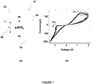
Figure 1 shows (a) a schematic cross-sectional view of an a-STOx MIM device produced in accordance with a preferred embodiment of the present invention, and (b) a chart illustrating a current-voltage relationship of an a-STOx MIM single layer device ofFigure 1 (a) comprising an oxygen-deficient amorphous-STOx (hereinafter referred to as a-STOx) switching layer thickness, L1, of 30 nm and a titanium cathode layer thickness, LT, of 5 nm, which reveals a representative bipolar resistive switching behaviour; -
Figure 2 shows (a) a schematic cross-sectional view of an a-STO x /a-STO bilayer MIM device produced in accordance with another preferred embodiment of the present invention, and charts illustrating a current-voltage relationship of the a-STOx/a-STO bilayer MIM device ofFigure 2(a) , which reveal (b) forward bipolar resistive switching behaviour, (c) complementary resistive switching behaviour, and (d) reverse bipolar resistive switching behaviour; and -
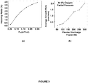
Figure 3 shows (a) a chart illustrating the rate of oxygen vacancy concentration vs. oxygen pressure for oxygen-deficient a-STOx switching layers deposited on a Si/SiO2 substrate by RF magnetron sputtering at room temperature, and (b) a chart illustrating the rate of growth of oxygen-deficient a-STOx switching layers vs. plasma discharge power at 0% oxygen partial pressure. - It should be noted in the following description that like or the same reference numerals in different embodiments denote the same or similar features.
- As shown in
Figure 1(a) there is provided a schematic cross-sectional view of a representative singlelayer memristor device 10 produced according to a preferred embodiment of the present invention. Thesingle layer device 10 is a stacked passive to terminal metal insulated metal (MIM) device or cell that comprises first andsecond electrodes layer MIM device 10. The first andsecond electrodes - In a preferred embodiment, the first and
second electrodes - As shown in
Figure 1(a) , the first ortop platinum electrode 20 has acathode metal layer 40 disposed on an inwardly facing surface thereof. Thecathode metal layer 40 is ideally a reactive low work function metal selected from the group consisting of platinum, palladium, gold, palladium-silver, ruthenium and iridium. - In a preferred embodiment, the
cathode metal layer 40 is formed from titanium metal having a thickness that falls within the range of 2 nm to 15 nm, more preferably, a thickness that falls within the range of 5 nm to 10 nm. - Disposed substantially between, and in electrical contact with, the second or
bottom platinum electrode 30 and thetitanium cathode layer 40 is an active region that comprises a switching layer in the form of anamorphous metal oxide 50. The amorphous metaloxide switching layer 50 takes the form of a near stoichiometric, oxygen-deficient amorphous perovskite ternary metal oxide layer of strontium titanate expressed by the formula amorphous-SrTiO3-x (hereinafter referred to as a-SrTiO3-x), wherein 0.05 < x < 0.15 (hereinafter, referred to in the shortened notational form as a-STOx). - In one embodiment, the oxygen-deficient a-STOx switching layer 50 has a thickness that falls within the range of 15 nm to 40 nm, more preferably, within the range of 15 nm to 30 nm, still more preferably, within the range of 15 nm to 25 nm.
- The inventors have found that a desirable requirement for achieving a versatile resistive switching single
layer MIM device 10 is low or no initial electrical stress (or electroforming voltage/current) to induce the metal-insulator transition in the singlelayer MIM device 10. As will be described below, three fabrication parameters may be employed to control the electroforming voltage/current threshold in the singlelayer MIM device 10 of the preferred embodiments of the present invention.
Control of the oxygen deficiency content in a-STO oxide switching layer: the synthesis technique of choice for depositing a-STO switching layers is RF magnetron sputtering in an Ar/O2 sputtering gas mixture using a stoichiometric SrTiO3 ceramic target. By controlling the background oxygen partial pressure in the RF plasma, the oxygen content in the depositeda-STO switching layer 50 can be controlled. The inventors have found that high oxygen deficiency content in the a-STOx switching layer 50 of a singlelayer MIM device 10 facilitates lower energy requirements for initial electroforming. -
Figure 3(a) shows a chart illustrating the dependence of the rate of oxygen vacancy concentration vs. oxygen pressure for oxygen-deficient a-STOx switching layers 50 deposited on a Si/SiO2 substrate by RF magnetron sputtering at room temperature. By virtue of being able to control the oxygen deficiency in theoxide switching layer 50 of the single layer andbilayer MIM devices - Control of oxide thickness/density: sputtering power, duration and target to substrate distance can be employed to control the oxide layer thickness and density during the RF sputtering deposition. With a moderate RF power (100W) and a large target to substrate distance (50 cm) in a "sputter-up" configuration, the thickness of the oxide layers can be controlled uniformly down to <5 nm. The oxygen-deficient a-STOx switching layer 50 used in the single
layer MIM device 10 may be varied in thickness between 10 and 40 nm and preferably between 15 and 40 nm to optimize the resistive switching performance of the resulting singlelayer MIM device 10. -
Figure 3(b) shows a chart illustrating the dependence of the rate of growth of oxygen-deficient a-STOx switching layers 50 vs. plasma discharge power at 0% oxygen partial pressure. By virtue of being able to control the thickness of the oxygen-deficient a-STOx switching layers 50 in the single layer orbilayer MIM devices - In short, the above approach allows precise control over the thickness of the oxygen-deficient a-STOx switching layer 50 and the oxygen deficiency concentration. In particular, using different oxygen partial pressures, the inventors have found that multi-layered or stacked films can be deposited on the substrate with ease. Since the deposition occurs at room temperature, inter-diffusion between the as-grown amorphous oxygen-deficient a-STOx switching layer 50 with defect vacancy profiles is unlikely, and in a worst case scenario, limited to 2-3 nm. Thus the electrical transport properties of each individual layer can be employed to optimize the overall stack's performance.
- Thickness of the cathode metal: the thickness of the
titanium cathode layer 40 in the singlelayer MIM device 10 influences the initial resistance and electrical characteristics of the singlelayer MIM device 10. At a critical thickness, the designed asymmetry in the singlelayer MIM device 10 allows for robust resistive switching at lower energies. - A method of fabricating a single
layer MIM device 10 according to a preferred embodiment of the present invention will now be described. - According to step 1) of the method, a
bottom platinum electrode 30 of 25 nm thickness is deposited onto a pre-patterned SiO2/Si substrate by electron beam evaporation at room temperature. Adhesion between the pre-patterned SiO2/Si substrate and thebottom platinum electrode 30 may be enhanced by virtue of depositing an adhesion promoting layer of TiO2 of thickness 5 nm onto the pre-patterned SiO2/Si substrate prior to applying thebottom platinum electrode 30. - According to step 2), an oxygen-deficient a-STOx switching layer 50 of 30 nm thickness is sputtered through a shadow mask onto the
bottom platinum electrode 30 by RF magnetron sputtering at room temperature in an Ar/O2 sputtering gas mixture using a stoichiometric SrTiO3 ceramic target at a base pressure of <10-7 Torr. - The inventors have found that a preferred partial pressure range to attain single phase perovskite oxide layers is 0-5%, whereupon a 5% oxygen partial pressure yields stoichiometric a-STO thin films and 0% partial pressure yields a maximum oxygen deficiency content of 3-4% in the
oxide switching layer 50. - Good results have been obtained for a single
layer MIM device 10 in which the oxygen-deficient switching layer (a-STOx) 50 is synthesized at 0% oxygen partial pressure and has a 3-4% oxygen deficiency content. - According to step 3), a
titanium cathode layer 40 of thickness 5 nm is first deposited onto the sputtered oxygen-deficient a-STOx switching layer 50 by electron beam evaporation at room temperature. - According to step 4), a
top platinum electrode 20 of thickness 25 nm is deposited onto thetitanium cathode layer 40 using the same electron beam evaporation apparatus, again at room temperature. - It will be appreciated by those skilled in the relevant art that the fabrication method described above is not limited to depositing the individual layers by sputtering, but that other deposition methods including thermal evaporation, electron beam evaporation, atomic layer deposition, co-deposition, chemical vapour deposition, ion beam assisted deposition, may also be employed.
- The inventors have found that by virtue of the
titanium cathode layer 40 being located between, and in electrical contact with, the topplatinum metal electrode 20 and the oxygen-deficient a-STOx switching layer 50, the resulting asymmetry within the singlelayer MIM device 10 enables a high-performance non-linear resistive switching to be achieved. - The thickness of the oxygen-deficient a-STOx switching layer 50 and the
titanium cathode layer 40 in the singlelayer MIM device 10 have been optimized to enable low voltage bipolar resistive switching behaviour. - Good results have been obtained for a single
layer MIM device 10 that comprises first andsecond platinum electrodes titanium cathode layer 40 having a thickness, LT, of 5 nm and an oxygen-deficient a-STOx layer 50 having a thickness, L1, of 30 nm. - The inventors have also found that when a switching voltage is applied between the first and
second platinum electrodes layer MIM device 10, the oxygen-deficient a-STOx switching layer 50 exhibits a bipolar resistive switching behaviour that occurs in one or both of a forward direction and a reverse direction. -
Figure 1(b) shows a chart illustrating a current-voltage relationship of a single layer a-STOx basedMIM device 10 having the above stated dimensions when a bias voltage is applied between the first andsecond electrodes layer MIM device 10. - At the origin of
Figure 1(b) , in which no bias voltage is applied, it will be appreciated that the singlelayer MIM device 10 persists in the OFF state. However, when a bias voltage is applied to the singlelayer MIM device 10 from about 0 V to about -1.5 V, biased from thetop platinum electrode 20, the singlelayer MIM device 10 experiences a path of high resistance (path 1) until the current reaches about -5 µA at a voltage of about -1 V. At this point, the singlelayer MIM device 10 switches to the ON state, where the current increases to about -330 µA until the voltage reaches - 1.5 V, corresponding to a low resistance state. When a voltage is subsequently applied from about 0 V to about +2 V, the current starts to decrease while the singlelayer MIM device 10 experiences a path of low resistance (along path 2). As the current and voltage pass through the origin and along path 3, the current increases to about +225 µA at a voltage of about +1.2 V. At this point, the singlelayer MIM device 10 switches to the OFF state, whereupon the current gradually decreases until the voltage reaches about +2 V. When the bias voltage is reduced to about 0 V, the OFF state is maintained as the current decreases back to zero and the singlelayer MIM device 10 experiences a path of high resistance (path 4). - The inventors have found that typical voltage ranges for achieving forward bipolar resistive switching in the single
layer MIM device 10 are around -1.5 V to +2 V. - Thus, when a voltage is applied in a negative polarity between the first and
second platinum electrodes top platinum electrode 30, the singlelayer MIM device 10 switches from a high resistance state to a low resistance state. On the other hand, when a voltage is applied in a positive polarity, again biased from thetop platinum electrode 30, the singlelayer MIM device 10 switches from a low resistance state to a high resistance state. This bipolar resistive switching behaviour may be performed repeatedly in the same manner, corresponding to a stable non-volatile bipolar switching characteristic, as indicated by the hysteresis resulting from the cycle of operation. - The inventors have found that the average OFF/ON switching ratio for the single
layer MIM device 10 is in the range of 102 to 103. - Whilst not wishing to be bound by any one particular theory, the bipolar switching behaviour of transition metal oxide layers in a stacked MIM device is generally perceived to be originating from inhomogeneous conduction mechanisms through localized filamentary pathways.
- In the case of the single
layer MIM device 10, by virtue of the controlled defect-rich structure of the a-STOx switching layer 50 resulting from the oxygen-deficiency, this allows a conductive filamentary pathway (not shown) to be formed between thebottom platinum electrode 30 and thetitanium cathode layer 40 of the singlelayer MIM device 10 when a sufficiently high bias voltage is applied between the first andsecond platinum electrodes layer MIM device 10 to provide desirable memristive properties. - As shown in
Figure 2(a) there is provided a schematic cross-sectional view of a representative bilayer layermemristor device 100 produced according to another preferred embodiment of the present invention. - The
bilayer MIM device 100 as shown inFigure 2(a) comprises the same or similar components that make up the singlelayer MIM device 10 described above, albeit with an additional amorphousmetal oxide layer 60 of strontium titanate, expressed by the formula a-SrTiO3 (hereinafter, referred to in the shortened notational form as a-STO), disposed substantially between thetitanium cathode layer 40 and the oxygen-deficient a-STOx switching layer 50. - Referring to the method of fabricating a single
layer MIM device 10 described above, prior to step 3) of this method, the fabrication of thebilayer MIM device 100 involves the additional step, step 3a), of depositing thea-STO switching layer 60 onto the oxygen-deficient a-STOx switching layer 50 by sputtering through a shadow mask using RF magnetron sputtering at room temperature in an Ar/O2 sputtering gas mixture using a stoichiometric SrTiO3 ceramic target at a base pressure of <10-7 Torr. - Good results have been obtained for a
bilayer MIM device 100 in which the oxygen-deficient switching layer (a-STOx) 50 is synthesized at 0% oxygen partial pressure and has a 3-4% oxygen deficiency content, while the stoichiometric (a-STO) switchinglayer 60 is synthesized at 5% partial pressure. The inventors have found that this combination is most suited to resistive switching device applications. - It will be understood by those skilled in the relevant art that the
titanium cathode layer 40 in thebilayer MIM device 100 performs according to the same or similar principles as in the singlelayer MIM device 10. - In one embodiment, each of the oxygen deficient a-STOx switching layer 50 and the
a-STO switching layer 60 of thebilayer MIM device 100 has a thickness that falls within the range of 15 nm to 40 nm, more preferably, within the range of 15 nm to 30 nm, still more preferably, within the range of 15 nm to 25 nm. - Good results have been obtained for a
bilayer MIM device 100 that comprises first andsecond platinum electrodes titanium cathode layer 40 having a thickness, LT, of 5 nm, ana-STO switching layer 60 having a thickness, L2, of 20 nm and an oxygen-deficient a-STOx switching layer 50 having a thickness, L1, of 20 nm. - Referring to
Figure 2(b) , there is shown a chart illustrating a current-voltage relationship of abilayer MIM device 100 having the above stated dimensions when a bias voltage is applied between the first andsecond platinum electrodes bilayer MIM device 100. - At the origin of
Figure 2(b) , in which no bias voltage is applied, it will be appreciated that thebilayer MIM device 100 persists in the OFF state. However, when a bias voltage is applied to thebilayer MIM device 100 from about 0 V to about -3 V, biased from thetop platinum electrode 20, thebilayer MIM device 100 experiences a path of high resistance (path 1) until the current reaches a limit of about -5 µA at a voltage of about -1.8 V. At this point, thebilayer MIM device 100 switches to the ON state, where the current increases to about -70 µA until the voltage reaches -2.5 V corresponding to a low resistance state. When a voltage is subsequently applied from about 0 V to about +4 V, the current starts to decrease and thebilayer MIM device 100 experiences a path of low resistance (along path 2). As the current and voltage pass through the origin and along path 3, the current increases to about +85 µA at a voltage of about +3.8 V. At this point, thebilayer MIM device 100 switches to the OFF state. When the bias voltage is reduced to about -0 V, the OFF state is maintained as the current falls back to zero as thebilayer MIM device 100 experiences a path of high resistance (path 4). Application of a bias voltage in the low voltage ranges before reaching switching thresholds may not disturb the switching state so that the device may be stable for READ operations. - The inventors have found that typical voltage ranges for achieving forward bipolar resistive switching in the
bilayer MIM device 100 are around -1.5 V to +3 V. - Thus, as in the case of the single layer MIM device 10 (see
Figure 1(b) ), when a voltage is applied in a negative polarity between the first andsecond platinum electrodes top platinum electrode 30, thebilayer MIM device 100 switches from a high resistance state to a low resistance state. On the other hand, when a voltage is applied in a positive polarity, again biased from thetop platinum electrode 30, thebilayer MIM device 100 switches from a low resistance state to a high resistance state. This bipolar resistive switching behaviour may be performed repeatedly in the same manner, corresponding to a stable non-volatile bipolar switching characteristic, as indicated by the hysteresis resulting from the cycle of operation. Application of a bias voltage in the low voltage ranges before reaching switching thresholds may not disturb the switching state so that the device may be stable for READ operations. - The inventors have found that the introduction of the additional
a-STO switching layer 60 further limits the overall conduction in thebilayer MIM device 100 in either switching regimes (low or high resistance) while keeping thebilayer MIM device 100 forming free. This may allow for resistive switching operation with lower energy requirements. - As in the case of the single
layer MIM device 10 described above, the inventors have found that by varying the thicknesses of each of the individual layers of thebilayer MIM device 100 it is possible to fine tune the memristive properties. Indeed, the inventors have found that switching ratios of up to 103 are achievable in thebilayer MIM device 100. - Another aspect of the
bilayer MIM device 100 is the potential for achieving complementary resistive switching and reversal of the switching polarity. - In the case of complementary resistive switching (CRS), and referring specifically to
Figure 2(c) , there is shown a chart illustrating a current-voltage relationship of a bilayerlayer MIM device 100 having the above stated dimensions when a bias voltage is applied between the first andsecond platinum electrodes bilayer MIM device 100. - The inventors have found that typical voltage ranges for achieving full range CRS-type switching in the
bilayer MIM device 100 are around -3 V to +3 V in one example. - Thus, as the chart in
Figure 2(c) reveals, by increasing the voltage in thebilayer MIM device 100, it can operate as a single cell CRS device. InFigure 2(c) VNTH1 indicates the start of a first or ON state switching region and VPTH1 indicates the start of a second or OFF state switching region (or vice versa). Conversely, VNTH2 indicates the end of the first or ON state switching region and VPTH1 indicates the end of the second or OFF state switching region (or vice versa). - In the case of reversal of the switching polarity of the
bilayer MIM device 100, and referring specifically toFigure 2(d) , there is shown a chart illustrating a current-voltage relationship of a bilayerlayer MIM device 100 having the above stated dimensions when a bias voltage is applied between the first andsecond platinum electrodes Figure 2(b) to Figure 2(d) and vice versa. - At the origin of
Figure 2(d) , in which no bias voltage is applied, it will be appreciated that thebilayer MIM device 100 persists in the OFF state. However, when a bias voltage is applied to thebilayer MIM device 100 from about 0 V to about +3 V, biased from thebottom platinum electrode 20, thebilayer MIM device 100 experiences a path of high resistance (path 1) until a voltage of about +1.7 V. At this point, thebilayer MIM device 100 switches to the ON state, where the current starts to increase until the voltage reaches +2.2 V resulting in a current of about +50 µA corresponding to a low resistance state. When a voltage is subsequently applied from about +3 V to about -5 V, the current starts to decrease and thebilayer MIM device 100 experiences a path of low resistance (alongpath 2, through the origin and along path 3) until the current reaches about -85 µA at a voltage of about -3.5 V. At this point, thebilayer MIM device 100 switches to the OFF state. When the bias voltage is increased to about +3 V again, the current falls back to zero as thebilayer MIM device 100 experiences a path of high resistance (path 4). The reversal may be achieved by applying a bias in the positive polarity equal to VPTH1 or in negative polarity equal to VNTH1. These two thresholds can be used to reverse the switching polarity fromFigure 2(b) to Figure 2(d) and vice versa. - The inventors have found that typical voltage ranges for reverse bipolar resistive switching in the
bilayer MIM device 100 are around -3 V to + 1.5 V. - Thus, when a voltage is applied in a positive polarity between the first and
second platinum electrodes top platinum electrode 30, thebilayer MIM device 100 switches from a low resistance state to a high resistance state. On the other hand, when a voltage is applied in a negative polarity, again biased from thetop platinum electrode 30, thebilayer MIM device 100 switches from a high resistance state to a low resistance state. This bipolar resistive switching behaviour is performed repeatedly in the same manner, corresponding to a stable non-volatile bipolar switching characteristic, as indicated by the hysteresis resulting from the cycle of operation. Application of a bias voltage in the low voltage ranges before reaching switching thresholds may not disturb the switching state so that the device may be stable for READ operations. - In short, the inventors have found that the same behaviour can be used to utilize the
bilayer MIM device 100 for switching in opposite polarities. - Again, whilst not wishing to be bound by any one particular theory, the inventors perceive that the complementary resistive switching (CRS) behaviour observed in the
bilayer MIM device 100 involves a reversal in the charge distribution and polarity of thea-STO switching layer 60 and the oxygen-deficient a-STOx switching layer 50, which infers that when one of the two oxide switching layers of thebilayer MIM device 100 is switched ON, the current flow causes the other oxide switching layer to switch OFF. This is in stark contrast to the result achieved employing the conventional approach of using two individual single layer MIM devices (not shown) connected together in an anti-serial manner. - On the other hand, if the voltage sweep applied between the first and
second platinum electrodes bilayer MIM device 100 is stopped once reaching the threshold for switching one of the two oxide switching layers ON (equally for pulse bias, if a voltage pulse is around the first threshold voltage), then that oxide switching layer (or interface) assumes the overall electrical behaviour of thebilayer MIM device 100, and as in the case of the singlelayer MIM device 10, it behaves as a bipolar switch. - If the polarity of the threshold voltage is changed, as is shown in the chart in
Figure 2(c) , in which there are threshold voltages in both polarities, then the polarity of the bipolar behaviour is also changed. This means that it is possible to operate thebilayer MIM device 100 in three distinct modes. - The single
layer MIM device 10 and thebilayer MIM device 100 fabricated according to the method of the present invention provide a number of distinct advantages over conventional STO-based memristor devices. - For instance, the single layer and
bilayer MIM devices - In addition, unlike conventional STO-based memristor devices, the single layer and
bilayer MIM devices - It is possible to fine tune the switching energy and ratio of the single layer and
bilayer MIM devices layer MIM device 10, and the thickness of one or both of the oxygen-deficient a-STOx switching layer 50 and thea- STO switching layer 60 in thebilayer MIM device 100. - The
bilayer MIM device 100 can be operated in three distinct modes: (i) forward bipolar resistive switching behaviour (ii) reverse bipolar resistive switching behaviour; and (iii) complementary resistive switching (CRS) behaviour. - It will be appreciated that the present invention is not limited to the embodiments described above but may include other embodiments.
- In another embodiment, it will be understood that the oxygen deficient a-STOx switching layer 50 of the single
layer MIM device 10, or one or both of the oxygen deficient a-STOx switching layer 50 and thea- STO switching layer 60 of thebilayer MIM device 100, may comprise doping atoms of a particular dopant element to further improve the energy requirements, stability, and controllability of the memristive performance of the single layer andbilayer MIM devices - In one embodiment, the ratio of titanium to niobium in the oxygen-deficient a-STOx switching layer 50 of the single
layer MIM device 10 is between 0.02 and 0.05.
the at least one layer of amorphous metal oxide includes an oxygen deficient amorphous metal oxide and the oxygen deficient amorphous metal oxide includes a strontium titanate expressed by a formula (amorphous -SrTiO3-x), wherein 0.05 < x < 0.15.
Claims (14)
- A memristor device (10, 100) comprising:- a first electrode (20);- a second electrode (30);- a cathode metal layer (40) disposed on a surface of the first electrode (20); and- an active region disposed between and in electrical contact with the second electrode (30) and the cathode metal layer (40), the active region comprising at least one layer of an amorphous metal oxide (50, 60);wherein
the memristor device (10, 100) is designed such that the active region exhibits a resistive switching behaviour when a switching voltage is applied between the first and second electrodes (20, 30), and
the at least one layer of amorphous metal oxide (50, 60) includes an oxygen deficient amorphous metal oxide;
characterized in that the oxygen deficient amorphous metal oxide includes a strontium titanate expressed by a formula amorphous-SrTiO3-x, wherein 0.05 < x < 0.15. - A memristor device (100) according to claim 1, wherein the at least one layer of amorphous metal oxide (50, 60) further comprises an amorphous metal oxide layer (60).
- A memristor device (100) according to claim 2, wherein the amorphous metal oxide layer (60) includes a strontium titanate expressed by a formula amorphous-SrTiO3.
- A memristor device (100) according to claim 2, wherein each of the oxygen deficient amorphous metal oxide layer (50) and the amorphous metal oxide layer (60) has a thickness that falls within the range of 15 nm to 40 nm.
- A memristor device (10, 100) according to any one of the preceding claims, wherein the oxygen deficient amorphous metal oxide comprises doping atoms of a dopant element selected from the group consisting of chromium and niobium.
- A memristor device (10, 100) according to claim 5, wherein the dopant element is niobium, and
wherein the ratio of niobium to titanium is between 0.02 and 0.05. - A memristor device (10, 100) according to claim 1, wherein the at least one layer of an amorphous metal oxide (50, 60) has a thickness that falls within the range of 15 nm to 40 nm.
- A memristor device (10, 100) according to any one of the preceding claims, wherein the cathode metal layer (40) has a thickness that falls within the range of 2 nm to 15 nm, preferably within the range of 5 nm to 10 nm.
- A memristor device (10, 100) according to any one of the preceding claims, wherein each of the first (20) and second electrodes (30) has a thickness that falls within the range of 25 nm to 35 nm.
- A memristor device (10, 100) according to any one of the preceding claims, wherein the resistive switching behaviour comprises a bipolar resistive switching behaviour that occurs in one or both of a forward direction and a reverse direction.
- A memristor device (10, 100) according to any one of claims 1 to 9, wherein the resistive switching behaviour comprises a bipolar resistive switching behaviour that occurs in one or more of a forward direction, a reverse direction, and a complementary resistive switching behaviour.
- A method of fabricating a memristor device (10, 100), the method comprising the steps of:a) providing a first electrode (20);b) providing a second electrode (30);c) providing a cathode metal layer (40) disposed on a surface of the first electrode (20); andd) providing an active region disposed between and in electrical contact with the second electrode (30) and the cathode metal layer (40), the active region comprising at least one layer of an amorphous metal oxide(50, 60);wherein
when a switching voltage is applied between the first and second electrodes (20, 30), the active region exhibits a resistive switching behaviour, and
the at least one layer of amorphous metal oxide (50, 60) includes an oxygen deficient amorphous metal oxide and the oxygen deficient amorphous metal oxide includes a strontium titanate expressed by a formula amorphous-SrTiO3-x, wherein 0.05 < x < 0.15. - A method of fabricating a memristor device (10, 100) according to claim 12, wherein one or more of steps a) to d) is conducted at room temperature.
- A method of fabricating a memristor device (10, 100) according to claim 12 or 13, wherein the resistive switching behaviour comprises a bipolar resistive switching behaviour that occurs in one or more of a forward direction, a reverse direction, and a complementary resistive switching behaviour.
Applications Claiming Priority (2)
| Application Number | Priority Date | Filing Date | Title |
|---|---|---|---|
| AU2015904857A AU2015904857A0 (en) | 2015-11-24 | A memristor device and a method of fabrication thereof | |
| PCT/AU2016/051145 WO2017088016A1 (en) | 2015-11-24 | 2016-11-23 | A memristor device and a method of fabrication thereof |
Publications (3)
| Publication Number | Publication Date |
|---|---|
| EP3381066A1 EP3381066A1 (en) | 2018-10-03 |
| EP3381066A4 EP3381066A4 (en) | 2019-07-24 |
| EP3381066B1 true EP3381066B1 (en) | 2021-04-28 |
Family
ID=58762863
Family Applications (1)
| Application Number | Title | Priority Date | Filing Date |
|---|---|---|---|
| EP16867449.7A Active EP3381066B1 (en) | 2015-11-24 | 2016-11-23 | A memristor device and a method of fabrication thereof |
Country Status (6)
| Country | Link |
|---|---|
| US (1) | US10985318B2 (en) |
| EP (1) | EP3381066B1 (en) |
| JP (1) | JP7020690B2 (en) |
| CN (1) | CN108475727A (en) |
| AU (1) | AU2016361453B2 (en) |
| WO (1) | WO2017088016A1 (en) |
Families Citing this family (12)
| Publication number | Priority date | Publication date | Assignee | Title |
|---|---|---|---|---|
| WO2018006131A1 (en) * | 2016-07-06 | 2018-01-11 | Rmit University | Multifunctional and multi-bit resistive storage memories |
| KR101922049B1 (en) * | 2018-01-25 | 2019-02-20 | 재단법인 대구경북과학기술원 | Artificial synapse element and manufacturing method thereof |
| CN108428700B (en) * | 2018-03-15 | 2020-11-24 | 西南交通大学 | A kind of preparation method of memristive and negative differential effect stable coexistence device at room temperature |
| CN108899418B (en) * | 2018-07-09 | 2022-02-15 | 广东工业大学 | Amorphous thin film device, preparation method and application thereof |
| US10930343B2 (en) | 2018-08-21 | 2021-02-23 | Hewlett Packard Enterprise Development Lp | Symmetric bipolar switching in memristors for artificial intelligence hardware |
| TWI694623B (en) * | 2019-07-10 | 2020-05-21 | 國立清華大學 | Halide semiconductor memristor and neuromorphic device |
| CN110600610A (en) * | 2019-09-26 | 2019-12-20 | 中国科学院微电子研究所 | Artificial neural synapse device and preparation method thereof |
| CN110911560B (en) * | 2019-11-29 | 2021-10-08 | 华中科技大学 | A planar memristor and method of making the same |
| US20230045427A1 (en) * | 2019-12-20 | 2023-02-09 | Royal Melbourne Institute Of Technology | Sensor for detecting a bioanalyte and a method for the detection thereof |
| CN115552423A (en) * | 2020-06-25 | 2022-12-30 | 睿纽摩菲斯公司 | Lithographic memristive array |
| CN112701220B (en) * | 2020-10-23 | 2024-02-06 | 大连理工大学 | A HfO2-based memristor with a metal Hf buffer layer and its manufacturing method |
| TWI773596B (en) * | 2021-11-24 | 2022-08-01 | 國立清華大學 | Lead-free metallic halide memristor and use thereof |
Family Cites Families (7)
| Publication number | Priority date | Publication date | Assignee | Title |
|---|---|---|---|---|
| FR2901601B1 (en) | 2006-05-24 | 2008-12-19 | Univ Grenoble 1 | ASSISTED ATOMIC STRENGTH MICROSCOPE |
| US8093575B2 (en) * | 2009-04-20 | 2012-01-10 | Hewlett-Packard Development Company, L.P. | Memristive device with a bi-metallic electrode |
| GB2471535B (en) | 2010-01-07 | 2012-01-11 | Dna Electronics Ltd | Electrically actuated switch |
| TW201408810A (en) * | 2012-07-12 | 2014-03-01 | 應用材料股份有限公司 | Method for depositing an oxygen-depleted metal film |
| KR101457812B1 (en) | 2013-08-19 | 2014-11-05 | 포항공과대학교 산학협력단 | 2-Terminal Switching Device Having Bipolar Switching Property, Fabrication Methods for the Same, and Resistance Memory Cross-Point Array Having the Same |
| US9793473B2 (en) * | 2013-09-05 | 2017-10-17 | Hewlett Packard Enterprise Development Lp | Memristor structures |
| US9899450B2 (en) * | 2015-09-15 | 2018-02-20 | The Regents Of The University Of California | Memristors and method for fabricating memristors |
-
2016
- 2016-11-23 AU AU2016361453A patent/AU2016361453B2/en not_active Ceased
- 2016-11-23 CN CN201680076329.3A patent/CN108475727A/en active Pending
- 2016-11-23 EP EP16867449.7A patent/EP3381066B1/en active Active
- 2016-11-23 WO PCT/AU2016/051145 patent/WO2017088016A1/en not_active Ceased
- 2016-11-23 US US15/778,776 patent/US10985318B2/en active Active
- 2016-11-23 JP JP2018545530A patent/JP7020690B2/en not_active Expired - Fee Related
Non-Patent Citations (1)
| Title |
|---|
| YAN X B ET AL: "Studies on the reset power needed for the unipolar resistive switching in amorphous SrTiOfilms induced by electrical pulse", PHYSICS LETTERS A, NORTH-HOLLAND PUBLISHING CO., AMSTERDAM, NL, vol. 375, no. 41, 16 July 2011 (2011-07-16), pages 3599 - 3603, XP028287805, ISSN: 0375-9601, [retrieved on 20110809], DOI: 10.1016/J.PHYSLETA.2011.07.031 * |
Also Published As
| Publication number | Publication date |
|---|---|
| JP2018538701A (en) | 2018-12-27 |
| US10985318B2 (en) | 2021-04-20 |
| EP3381066A4 (en) | 2019-07-24 |
| CN108475727A (en) | 2018-08-31 |
| US20180351095A1 (en) | 2018-12-06 |
| EP3381066A1 (en) | 2018-10-03 |
| JP7020690B2 (en) | 2022-02-16 |
| AU2016361453B2 (en) | 2022-05-12 |
| WO2017088016A1 (en) | 2017-06-01 |
| AU2016361453A1 (en) | 2018-06-14 |
Similar Documents
| Publication | Publication Date | Title |
|---|---|---|
| AU2016361453B2 (en) | A memristor device and a method of fabrication thereof | |
| US9818939B2 (en) | Resistive switching devices having a switching layer and an intermediate electrode layer and methods of formation thereof | |
| KR100693409B1 (en) | Nonvolatile Memory Device and Manufacturing Method Using Changed Resistance of Oxide Film | |
| JP2018538701A5 (en) | ||
| EP3602561B1 (en) | A switching resistor and method of making such a device | |
| US9281477B2 (en) | Resistance change element and method for producing the same | |
| US8749023B2 (en) | Resistance-variable memory device and a production method therefor | |
| JP2018511164A (en) | Materials and components in phase change memory devices | |
| US12396375B2 (en) | Resistive random-access memory devices with engineered electronic defects and methods for making the same | |
| Chabungbam et al. | Enhanced memory window and efficient resistive switching in stabilized BaTiO3-based RRAM through incorporation of Al2O3 interlayer | |
| Ahn et al. | Resistive random access memory characteristics of NiO thin films with an oxygen-deficient NiO0. 95 layer | |
| US8487289B2 (en) | Electrically actuated device | |
| KR102834838B1 (en) | Resistive random access memory device having engineered electronic defects and method for fabricating the same | |
| KR101176422B1 (en) | Nonvolatile resistance random access memory device | |
| Tranchant et al. | Mott memory devices based on the Mott insulator (V1-xCrx) 2O3 | |
| KR102497052B1 (en) | Resistive switching memory device having halide perovskite and method of manufacturing the same | |
| US20250143194A1 (en) | Resistive random-access memory (rram) devices with doped switching oxides | |
| US20250160222A1 (en) | Deuterium-treated resistive random-access memory (rram) devices | |
| WO2018006131A1 (en) | Multifunctional and multi-bit resistive storage memories | |
| CN116709896A (en) | Amorphous Nb-based chalcogenide semiconductor and self-repairing conductive bridge resistive random access memory | |
| Benko et al. | The influence of ozone pre-treatment in HfO 2-based resistive switching memory structures |
Legal Events
| Date | Code | Title | Description |
|---|---|---|---|
| STAA | Information on the status of an ep patent application or granted ep patent |
Free format text: STATUS: THE INTERNATIONAL PUBLICATION HAS BEEN MADE |
|
| PUAI | Public reference made under article 153(3) epc to a published international application that has entered the european phase |
Free format text: ORIGINAL CODE: 0009012 |
|
| STAA | Information on the status of an ep patent application or granted ep patent |
Free format text: STATUS: REQUEST FOR EXAMINATION WAS MADE |
|
| 17P | Request for examination filed |
Effective date: 20180620 |
|
| AK | Designated contracting states |
Kind code of ref document: A1 Designated state(s): AL AT BE BG CH CY CZ DE DK EE ES FI FR GB GR HR HU IE IS IT LI LT LU LV MC MK MT NL NO PL PT RO RS SE SI SK SM TR |
|
| AX | Request for extension of the european patent |
Extension state: BA ME |
|
| DAV | Request for validation of the european patent (deleted) | ||
| DAX | Request for extension of the european patent (deleted) | ||
| A4 | Supplementary search report drawn up and despatched |
Effective date: 20190621 |
|
| RIC1 | Information provided on ipc code assigned before grant |
Ipc: H01L 45/00 20060101AFI20190614BHEP |
|
| GRAP | Despatch of communication of intention to grant a patent |
Free format text: ORIGINAL CODE: EPIDOSNIGR1 |
|
| STAA | Information on the status of an ep patent application or granted ep patent |
Free format text: STATUS: GRANT OF PATENT IS INTENDED |
|
| INTG | Intention to grant announced |
Effective date: 20200622 |
|
| GRAJ | Information related to disapproval of communication of intention to grant by the applicant or resumption of examination proceedings by the epo deleted |
Free format text: ORIGINAL CODE: EPIDOSDIGR1 |
|
| STAA | Information on the status of an ep patent application or granted ep patent |
Free format text: STATUS: REQUEST FOR EXAMINATION WAS MADE |
|
| GRAP | Despatch of communication of intention to grant a patent |
Free format text: ORIGINAL CODE: EPIDOSNIGR1 |
|
| STAA | Information on the status of an ep patent application or granted ep patent |
Free format text: STATUS: GRANT OF PATENT IS INTENDED |
|
| INTC | Intention to grant announced (deleted) | ||
| INTG | Intention to grant announced |
Effective date: 20201117 |
|
| GRAS | Grant fee paid |
Free format text: ORIGINAL CODE: EPIDOSNIGR3 |
|
| GRAA | (expected) grant |
Free format text: ORIGINAL CODE: 0009210 |
|
| STAA | Information on the status of an ep patent application or granted ep patent |
Free format text: STATUS: THE PATENT HAS BEEN GRANTED |
|
| AK | Designated contracting states |
Kind code of ref document: B1 Designated state(s): AL AT BE BG CH CY CZ DE DK EE ES FI FR GB GR HR HU IE IS IT LI LT LU LV MC MK MT NL NO PL PT RO RS SE SI SK SM TR |
|
| REG | Reference to a national code |
Ref country code: GB Ref legal event code: FG4D |
|
| REG | Reference to a national code |
Ref country code: CH Ref legal event code: EP |
|
| REG | Reference to a national code |
Ref country code: AT Ref legal event code: REF Ref document number: 1388108 Country of ref document: AT Kind code of ref document: T Effective date: 20210515 |
|
| REG | Reference to a national code |
Ref country code: DE Ref legal event code: R096 Ref document number: 602016057110 Country of ref document: DE |
|
| REG | Reference to a national code |
Ref country code: IE Ref legal event code: FG4D |
|
| REG | Reference to a national code |
Ref country code: NL Ref legal event code: FP |
|
| REG | Reference to a national code |
Ref country code: LT Ref legal event code: MG9D |
|
| REG | Reference to a national code |
Ref country code: AT Ref legal event code: MK05 Ref document number: 1388108 Country of ref document: AT Kind code of ref document: T Effective date: 20210428 |
|
| PG25 | Lapsed in a contracting state [announced via postgrant information from national office to epo] |
Ref country code: LT Free format text: LAPSE BECAUSE OF FAILURE TO SUBMIT A TRANSLATION OF THE DESCRIPTION OR TO PAY THE FEE WITHIN THE PRESCRIBED TIME-LIMIT Effective date: 20210428 Ref country code: FI Free format text: LAPSE BECAUSE OF FAILURE TO SUBMIT A TRANSLATION OF THE DESCRIPTION OR TO PAY THE FEE WITHIN THE PRESCRIBED TIME-LIMIT Effective date: 20210428 Ref country code: HR Free format text: LAPSE BECAUSE OF FAILURE TO SUBMIT A TRANSLATION OF THE DESCRIPTION OR TO PAY THE FEE WITHIN THE PRESCRIBED TIME-LIMIT Effective date: 20210428 Ref country code: BG Free format text: LAPSE BECAUSE OF FAILURE TO SUBMIT A TRANSLATION OF THE DESCRIPTION OR TO PAY THE FEE WITHIN THE PRESCRIBED TIME-LIMIT Effective date: 20210728 Ref country code: AT Free format text: LAPSE BECAUSE OF FAILURE TO SUBMIT A TRANSLATION OF THE DESCRIPTION OR TO PAY THE FEE WITHIN THE PRESCRIBED TIME-LIMIT Effective date: 20210428 |
|
| PG25 | Lapsed in a contracting state [announced via postgrant information from national office to epo] |
Ref country code: GR Free format text: LAPSE BECAUSE OF FAILURE TO SUBMIT A TRANSLATION OF THE DESCRIPTION OR TO PAY THE FEE WITHIN THE PRESCRIBED TIME-LIMIT Effective date: 20210729 Ref country code: IS Free format text: LAPSE BECAUSE OF FAILURE TO SUBMIT A TRANSLATION OF THE DESCRIPTION OR TO PAY THE FEE WITHIN THE PRESCRIBED TIME-LIMIT Effective date: 20210828 Ref country code: LV Free format text: LAPSE BECAUSE OF FAILURE TO SUBMIT A TRANSLATION OF THE DESCRIPTION OR TO PAY THE FEE WITHIN THE PRESCRIBED TIME-LIMIT Effective date: 20210428 Ref country code: PT Free format text: LAPSE BECAUSE OF FAILURE TO SUBMIT A TRANSLATION OF THE DESCRIPTION OR TO PAY THE FEE WITHIN THE PRESCRIBED TIME-LIMIT Effective date: 20210830 Ref country code: PL Free format text: LAPSE BECAUSE OF FAILURE TO SUBMIT A TRANSLATION OF THE DESCRIPTION OR TO PAY THE FEE WITHIN THE PRESCRIBED TIME-LIMIT Effective date: 20210428 Ref country code: NO Free format text: LAPSE BECAUSE OF FAILURE TO SUBMIT A TRANSLATION OF THE DESCRIPTION OR TO PAY THE FEE WITHIN THE PRESCRIBED TIME-LIMIT Effective date: 20210728 Ref country code: SE Free format text: LAPSE BECAUSE OF FAILURE TO SUBMIT A TRANSLATION OF THE DESCRIPTION OR TO PAY THE FEE WITHIN THE PRESCRIBED TIME-LIMIT Effective date: 20210428 Ref country code: RS Free format text: LAPSE BECAUSE OF FAILURE TO SUBMIT A TRANSLATION OF THE DESCRIPTION OR TO PAY THE FEE WITHIN THE PRESCRIBED TIME-LIMIT Effective date: 20210428 |
|
| PG25 | Lapsed in a contracting state [announced via postgrant information from national office to epo] |
Ref country code: DK Free format text: LAPSE BECAUSE OF FAILURE TO SUBMIT A TRANSLATION OF THE DESCRIPTION OR TO PAY THE FEE WITHIN THE PRESCRIBED TIME-LIMIT Effective date: 20210428 Ref country code: CZ Free format text: LAPSE BECAUSE OF FAILURE TO SUBMIT A TRANSLATION OF THE DESCRIPTION OR TO PAY THE FEE WITHIN THE PRESCRIBED TIME-LIMIT Effective date: 20210428 Ref country code: EE Free format text: LAPSE BECAUSE OF FAILURE TO SUBMIT A TRANSLATION OF THE DESCRIPTION OR TO PAY THE FEE WITHIN THE PRESCRIBED TIME-LIMIT Effective date: 20210428 Ref country code: ES Free format text: LAPSE BECAUSE OF FAILURE TO SUBMIT A TRANSLATION OF THE DESCRIPTION OR TO PAY THE FEE WITHIN THE PRESCRIBED TIME-LIMIT Effective date: 20210428 Ref country code: RO Free format text: LAPSE BECAUSE OF FAILURE TO SUBMIT A TRANSLATION OF THE DESCRIPTION OR TO PAY THE FEE WITHIN THE PRESCRIBED TIME-LIMIT Effective date: 20210428 Ref country code: SM Free format text: LAPSE BECAUSE OF FAILURE TO SUBMIT A TRANSLATION OF THE DESCRIPTION OR TO PAY THE FEE WITHIN THE PRESCRIBED TIME-LIMIT Effective date: 20210428 Ref country code: SK Free format text: LAPSE BECAUSE OF FAILURE TO SUBMIT A TRANSLATION OF THE DESCRIPTION OR TO PAY THE FEE WITHIN THE PRESCRIBED TIME-LIMIT Effective date: 20210428 |
|
| REG | Reference to a national code |
Ref country code: DE Ref legal event code: R097 Ref document number: 602016057110 Country of ref document: DE |
|
| PLBE | No opposition filed within time limit |
Free format text: ORIGINAL CODE: 0009261 |
|
| STAA | Information on the status of an ep patent application or granted ep patent |
Free format text: STATUS: NO OPPOSITION FILED WITHIN TIME LIMIT |
|
| 26N | No opposition filed |
Effective date: 20220131 |
|
| PG25 | Lapsed in a contracting state [announced via postgrant information from national office to epo] |
Ref country code: IS Free format text: LAPSE BECAUSE OF FAILURE TO SUBMIT A TRANSLATION OF THE DESCRIPTION OR TO PAY THE FEE WITHIN THE PRESCRIBED TIME-LIMIT Effective date: 20210828 Ref country code: AL Free format text: LAPSE BECAUSE OF FAILURE TO SUBMIT A TRANSLATION OF THE DESCRIPTION OR TO PAY THE FEE WITHIN THE PRESCRIBED TIME-LIMIT Effective date: 20210428 |
|
| PG25 | Lapsed in a contracting state [announced via postgrant information from national office to epo] |
Ref country code: MC Free format text: LAPSE BECAUSE OF FAILURE TO SUBMIT A TRANSLATION OF THE DESCRIPTION OR TO PAY THE FEE WITHIN THE PRESCRIBED TIME-LIMIT Effective date: 20210428 |
|
| REG | Reference to a national code |
Ref country code: CH Ref legal event code: PL |
|
| PG25 | Lapsed in a contracting state [announced via postgrant information from national office to epo] |
Ref country code: LU Free format text: LAPSE BECAUSE OF NON-PAYMENT OF DUE FEES Effective date: 20211123 Ref country code: IT Free format text: LAPSE BECAUSE OF FAILURE TO SUBMIT A TRANSLATION OF THE DESCRIPTION OR TO PAY THE FEE WITHIN THE PRESCRIBED TIME-LIMIT Effective date: 20210428 Ref country code: BE Free format text: LAPSE BECAUSE OF NON-PAYMENT OF DUE FEES Effective date: 20211130 |
|
| REG | Reference to a national code |
Ref country code: BE Ref legal event code: MM Effective date: 20211130 |
|
| PG25 | Lapsed in a contracting state [announced via postgrant information from national office to epo] |
Ref country code: IE Free format text: LAPSE BECAUSE OF NON-PAYMENT OF DUE FEES Effective date: 20211123 |
|
| REG | Reference to a national code |
Ref country code: DE Ref legal event code: R079 Ref document number: 602016057110 Country of ref document: DE Free format text: PREVIOUS MAIN CLASS: H01L0045000000 Ipc: H10N0070000000 |
|
| PG25 | Lapsed in a contracting state [announced via postgrant information from national office to epo] |
Ref country code: HU Free format text: LAPSE BECAUSE OF FAILURE TO SUBMIT A TRANSLATION OF THE DESCRIPTION OR TO PAY THE FEE WITHIN THE PRESCRIBED TIME-LIMIT; INVALID AB INITIO Effective date: 20161123 |
|
| PG25 | Lapsed in a contracting state [announced via postgrant information from national office to epo] |
Ref country code: CY Free format text: LAPSE BECAUSE OF FAILURE TO SUBMIT A TRANSLATION OF THE DESCRIPTION OR TO PAY THE FEE WITHIN THE PRESCRIBED TIME-LIMIT Effective date: 20210428 |
|
| PG25 | Lapsed in a contracting state [announced via postgrant information from national office to epo] |
Ref country code: LI Free format text: LAPSE BECAUSE OF NON-PAYMENT OF DUE FEES Effective date: 20220630 Ref country code: CH Free format text: LAPSE BECAUSE OF NON-PAYMENT OF DUE FEES Effective date: 20220630 |
|
| P01 | Opt-out of the competence of the unified patent court (upc) registered |
Effective date: 20230830 |
|
| PGFP | Annual fee paid to national office [announced via postgrant information from national office to epo] |
Ref country code: NL Payment date: 20231127 Year of fee payment: 8 |
|
| PGFP | Annual fee paid to national office [announced via postgrant information from national office to epo] |
Ref country code: GB Payment date: 20231128 Year of fee payment: 8 |
|
| PGFP | Annual fee paid to national office [announced via postgrant information from national office to epo] |
Ref country code: FR Payment date: 20231129 Year of fee payment: 8 Ref country code: DE Payment date: 20231201 Year of fee payment: 8 |
|
| PG25 | Lapsed in a contracting state [announced via postgrant information from national office to epo] |
Ref country code: MK Free format text: LAPSE BECAUSE OF FAILURE TO SUBMIT A TRANSLATION OF THE DESCRIPTION OR TO PAY THE FEE WITHIN THE PRESCRIBED TIME-LIMIT Effective date: 20210428 |
|
| PG25 | Lapsed in a contracting state [announced via postgrant information from national office to epo] |
Ref country code: MT Free format text: LAPSE BECAUSE OF FAILURE TO SUBMIT A TRANSLATION OF THE DESCRIPTION OR TO PAY THE FEE WITHIN THE PRESCRIBED TIME-LIMIT Effective date: 20210428 |
|
| REG | Reference to a national code |
Ref country code: DE Ref legal event code: R119 Ref document number: 602016057110 Country of ref document: DE |
|
| REG | Reference to a national code |
Ref country code: NL Ref legal event code: MM Effective date: 20241201 |
|
| GBPC | Gb: european patent ceased through non-payment of renewal fee |
Effective date: 20241123 |
|
| PG25 | Lapsed in a contracting state [announced via postgrant information from national office to epo] |
Ref country code: NL Free format text: LAPSE BECAUSE OF NON-PAYMENT OF DUE FEES Effective date: 20241201 |
|
| PG25 | Lapsed in a contracting state [announced via postgrant information from national office to epo] |
Ref country code: DE Free format text: LAPSE BECAUSE OF NON-PAYMENT OF DUE FEES Effective date: 20250603 |
|
| PG25 | Lapsed in a contracting state [announced via postgrant information from national office to epo] |
Ref country code: GB Free format text: LAPSE BECAUSE OF NON-PAYMENT OF DUE FEES Effective date: 20241123 |
|
| PG25 | Lapsed in a contracting state [announced via postgrant information from national office to epo] |
Ref country code: FR Free format text: LAPSE BECAUSE OF NON-PAYMENT OF DUE FEES Effective date: 20241130 |
|
| PG25 | Lapsed in a contracting state [announced via postgrant information from national office to epo] |
Ref country code: TR Free format text: LAPSE BECAUSE OF FAILURE TO SUBMIT A TRANSLATION OF THE DESCRIPTION OR TO PAY THE FEE WITHIN THE PRESCRIBED TIME-LIMIT Effective date: 20210428 |