EP3379733B1 - Elektronische vorrichtung und betriebsverfahren dafür - Google Patents
Elektronische vorrichtung und betriebsverfahren dafür Download PDFInfo
- Publication number
- EP3379733B1 EP3379733B1 EP16866615.4A EP16866615A EP3379733B1 EP 3379733 B1 EP3379733 B1 EP 3379733B1 EP 16866615 A EP16866615 A EP 16866615A EP 3379733 B1 EP3379733 B1 EP 3379733B1
- Authority
- EP
- European Patent Office
- Prior art keywords
- antenna
- magnetic field
- field module
- electronic device
- module
- Prior art date
- Legal status (The legal status is an assumption and is not a legal conclusion. Google has not performed a legal analysis and makes no representation as to the accuracy of the status listed.)
- Active
Links
Images








Classifications
-
- H—ELECTRICITY
- H02—GENERATION; CONVERSION OR DISTRIBUTION OF ELECTRIC POWER
- H02J—ELECTRIC POWER NETWORKS; CIRCUIT ARRANGEMENTS OR SYSTEMS FOR SUPPLYING OR DISTRIBUTING ELECTRIC POWER; SYSTEMS FOR STORING ELECTRIC ENERGY
- H02J50/00—Circuit arrangements or systems for wireless supply or distribution of electric power
- H02J50/10—Circuit arrangements or systems for wireless supply or distribution of electric power using inductive coupling
- H02J50/12—Circuit arrangements or systems for wireless supply or distribution of electric power using inductive coupling of the resonant type
-
- H—ELECTRICITY
- H01—ELECTRIC ELEMENTS
- H01F—MAGNETS; INDUCTANCES; TRANSFORMERS; SELECTION OF MATERIALS FOR THEIR MAGNETIC PROPERTIES
- H01F27/00—Details of transformers or inductances, in general
- H01F27/34—Special means for preventing or reducing unwanted electric or magnetic effects, e.g. no-load losses, reactive currents, harmonics, oscillations, leakage fields
- H01F27/36—Electric or magnetic shields or screens
-
- H—ELECTRICITY
- H01—ELECTRIC ELEMENTS
- H01F—MAGNETS; INDUCTANCES; TRANSFORMERS; SELECTION OF MATERIALS FOR THEIR MAGNETIC PROPERTIES
- H01F27/00—Details of transformers or inductances, in general
- H01F27/34—Special means for preventing or reducing unwanted electric or magnetic effects, e.g. no-load losses, reactive currents, harmonics, oscillations, leakage fields
- H01F27/36—Electric or magnetic shields or screens
- H01F27/361—Electric or magnetic shields or screens made of combinations of electrically conductive material and ferromagnetic material
-
- H—ELECTRICITY
- H01—ELECTRIC ELEMENTS
- H01F—MAGNETS; INDUCTANCES; TRANSFORMERS; SELECTION OF MATERIALS FOR THEIR MAGNETIC PROPERTIES
- H01F27/00—Details of transformers or inductances, in general
- H01F27/34—Special means for preventing or reducing unwanted electric or magnetic effects, e.g. no-load losses, reactive currents, harmonics, oscillations, leakage fields
- H01F27/36—Electric or magnetic shields or screens
- H01F27/363—Electric or magnetic shields or screens made of electrically conductive material
-
- H—ELECTRICITY
- H01—ELECTRIC ELEMENTS
- H01F—MAGNETS; INDUCTANCES; TRANSFORMERS; SELECTION OF MATERIALS FOR THEIR MAGNETIC PROPERTIES
- H01F27/00—Details of transformers or inductances, in general
- H01F27/34—Special means for preventing or reducing unwanted electric or magnetic effects, e.g. no-load losses, reactive currents, harmonics, oscillations, leakage fields
- H01F27/36—Electric or magnetic shields or screens
- H01F27/366—Electric or magnetic shields or screens made of ferromagnetic material
-
- H—ELECTRICITY
- H01—ELECTRIC ELEMENTS
- H01F—MAGNETS; INDUCTANCES; TRANSFORMERS; SELECTION OF MATERIALS FOR THEIR MAGNETIC PROPERTIES
- H01F38/00—Adaptations of transformers or inductances for specific applications or functions
- H01F38/14—Inductive couplings
-
- H—ELECTRICITY
- H01—ELECTRIC ELEMENTS
- H01F—MAGNETS; INDUCTANCES; TRANSFORMERS; SELECTION OF MATERIALS FOR THEIR MAGNETIC PROPERTIES
- H01F5/00—Coils
- H01F5/003—Printed circuit coils
-
- H—ELECTRICITY
- H02—GENERATION; CONVERSION OR DISTRIBUTION OF ELECTRIC POWER
- H02J—ELECTRIC POWER NETWORKS; CIRCUIT ARRANGEMENTS OR SYSTEMS FOR SUPPLYING OR DISTRIBUTING ELECTRIC POWER; SYSTEMS FOR STORING ELECTRIC ENERGY
- H02J50/00—Circuit arrangements or systems for wireless supply or distribution of electric power
- H02J50/005—Mechanical details of housing or structure aiming to accommodate the power transfer means, e.g. mechanical integration of coils, antennas or transducers into emitting or receiving devices
-
- H—ELECTRICITY
- H02—GENERATION; CONVERSION OR DISTRIBUTION OF ELECTRIC POWER
- H02J—ELECTRIC POWER NETWORKS; CIRCUIT ARRANGEMENTS OR SYSTEMS FOR SUPPLYING OR DISTRIBUTING ELECTRIC POWER; SYSTEMS FOR STORING ELECTRIC ENERGY
- H02J50/00—Circuit arrangements or systems for wireless supply or distribution of electric power
- H02J50/20—Circuit arrangements or systems for wireless supply or distribution of electric power using microwaves or radio frequency waves
-
- H—ELECTRICITY
- H02—GENERATION; CONVERSION OR DISTRIBUTION OF ELECTRIC POWER
- H02J—ELECTRIC POWER NETWORKS; CIRCUIT ARRANGEMENTS OR SYSTEMS FOR SUPPLYING OR DISTRIBUTING ELECTRIC POWER; SYSTEMS FOR STORING ELECTRIC ENERGY
- H02J50/00—Circuit arrangements or systems for wireless supply or distribution of electric power
- H02J50/40—Circuit arrangements or systems for wireless supply or distribution of electric power using two or more transmitting or receiving devices
- H02J50/402—Circuit arrangements or systems for wireless supply or distribution of electric power using two or more transmitting or receiving devices the two or more transmitting or the two or more receiving devices being integrated in the same unit, e.g. power mats with several coils or antennas with several sub-antennas
-
- H—ELECTRICITY
- H02—GENERATION; CONVERSION OR DISTRIBUTION OF ELECTRIC POWER
- H02J—ELECTRIC POWER NETWORKS; CIRCUIT ARRANGEMENTS OR SYSTEMS FOR SUPPLYING OR DISTRIBUTING ELECTRIC POWER; SYSTEMS FOR STORING ELECTRIC ENERGY
- H02J50/00—Circuit arrangements or systems for wireless supply or distribution of electric power
- H02J50/70—Circuit arrangements or systems for wireless supply or distribution of electric power involving the reduction of electric, magnetic or electromagnetic leakage fields
-
- H—ELECTRICITY
- H02—GENERATION; CONVERSION OR DISTRIBUTION OF ELECTRIC POWER
- H02J—ELECTRIC POWER NETWORKS; CIRCUIT ARRANGEMENTS OR SYSTEMS FOR SUPPLYING OR DISTRIBUTING ELECTRIC POWER; SYSTEMS FOR STORING ELECTRIC ENERGY
- H02J50/00—Circuit arrangements or systems for wireless supply or distribution of electric power
- H02J50/80—Circuit arrangements or systems for wireless supply or distribution of electric power involving the exchange of data, concerning supply or distribution of electric power, between transmitting devices and receiving devices
-
- H—ELECTRICITY
- H02—GENERATION; CONVERSION OR DISTRIBUTION OF ELECTRIC POWER
- H02J—ELECTRIC POWER NETWORKS; CIRCUIT ARRANGEMENTS OR SYSTEMS FOR SUPPLYING OR DISTRIBUTING ELECTRIC POWER; SYSTEMS FOR STORING ELECTRIC ENERGY
- H02J7/00—Circuit arrangements for charging or discharging batteries or for supplying loads from batteries
- H02J7/40—Circuit arrangements for charging or discharging batteries or for supplying loads from batteries characterised by the exchange of charge or discharge related data
- H02J7/42—Circuit arrangements for charging or discharging batteries or for supplying loads from batteries characterised by the exchange of charge or discharge related data with electronic devices having internal batteries, e.g. mobile phones
-
- H—ELECTRICITY
- H04—ELECTRIC COMMUNICATION TECHNIQUE
- H04B—TRANSMISSION
- H04B5/00—Near-field transmission systems, e.g. inductive or capacitive transmission systems
- H04B5/20—Near-field transmission systems, e.g. inductive or capacitive transmission systems characterised by the transmission technique; characterised by the transmission medium
- H04B5/24—Inductive coupling
- H04B5/26—Inductive coupling using coils
-
- H—ELECTRICITY
- H04—ELECTRIC COMMUNICATION TECHNIQUE
- H04B—TRANSMISSION
- H04B5/00—Near-field transmission systems, e.g. inductive or capacitive transmission systems
- H04B5/70—Near-field transmission systems, e.g. inductive or capacitive transmission systems specially adapted for specific purposes
- H04B5/79—Near-field transmission systems, e.g. inductive or capacitive transmission systems specially adapted for specific purposes for data transfer in combination with power transfer
Definitions
- Various embodiments relate to an electronic device and an operating method thereof.
- the electronic device may receive power wirelessly.
- the electronic device may receive the power by using a magnetic field.
- the electronic device may perform short range communication.
- the electronic device may perform the short range communication by using the magnetic field.
- the electronic device may include a plurality of modules and a plurality of coils.
- the modules may respectively correspond to the coils.
- US 2015/0065041 A1 discloses a portable device using a common antenna for both near field communication and wireless charging.
- the portable device includes: a common antenna part transmitting and receiving near field communication and wireless charging signals; an NFC signal judgment module connected to the common antenna part and sensing a signal applied from the common antenna part or a Tx signal generated from an NFC performing part to thereby judge whether or not the signal applied from the common antenna part or the Tx signal is the near field communication signal.
- US 2009/0001930 A1 discloses an apparatus for receiving electromagnetically induced current, the apparatus comprising an antenna element for receiving electromagnetically induced current in a first apparatus operating mode, and also for near field communication in a second apparatus operating mode, wherein the apparatus comprises circuitry for switching the apparatus from the second apparatus operating mode to the first apparatus operating mode based on near field communication signaling received via the antenna element in the second apparatus operating mode.
- JP 2013214870 A discloses a radio terminal which detects whether it is in contact with an external device. In case the radio terminal is not in contact with the external device, a first transmission part is used for radio communication by resonating at a first frequency. In case the radio terminal is in contact with the external device, a second transmission part is used for radio communication by resonating at a second frequency higher than the first frequency.
- a space for mounting coils is required in the aforementioned electronic device.
- the space for mounting the coils in the electronic device may be increased in proportion to the number of coils.
- a material cost for mounting the coils is required in the aforementioned electronic device.
- the material cost for mounting the coils in the electronic device may be increased in proportion to the number of coils.
- an interference may occur between modules through the coils in the electronic device. Accordingly, performance of the modules may deteriorate in the electronic device.
- An electronic device is provided, according to claim 1.
- a method of operating an electronic device is provided, according to claim 9.
- an electronic device may commonly use one coil in a plurality of magnetic field communication and charging schemes. Therefore, since a space for mounting the coil in the electronic device can be decreased, the electronic device can be implemented to have a compact size. In addition, a material cost for mounting the coil in the electronic device can be decreased.
- the electronic device may be designed by increasing a width of a winding of the coil since the space for mounting the coil is ensured, thereby decreasing a resistance component of the coil in the electronic device. Accordingly, performance of the coil can be improved in the electronic device.
- the electronic device controls a connection between modules, thereby avoiding an interference between the modules. That is, the modules can be separated from each other in the electronic device. Accordingly, performance of the modules can be improved in the electronic device.
- any constituent element may modify corresponding constituent elements irrespective of order and/or importance, and are just used to distinguish one constituent element from another constituent element and do not limit the corresponding constituent elements.
- any constituent element e.g., 1st
- the any constituent element may be directly coupled to the another constituent element, or be coupled through a further constituent element (e.g., a third constituent element).
- the expression “configured (or set) to ⁇ ” used in the present document may be used interchangeably with, for example, “suitable for-”, “having the capacity to ⁇ ", “designed to ⁇ ”, “adapted to ⁇ ”, “made to ⁇ ”, or “capable of ⁇ ” in a hardware or software manner in accordance to circumstances.
- the expression “device configured to ⁇ ” may represent that the device is “capable of ⁇ ” together with other devices or components.
- processor configured (or set) to perform A, B and C may represent an exclusive processor (e.g., embedded processor) for performing a corresponding operation, or a generic-purpose processor (e.g., a central processing unit (CPU) or an application processor (AP)) capable of performing corresponding operations by executing one or more software programs stored in a memory device.
- an exclusive processor e.g., embedded processor
- a generic-purpose processor e.g., a central processing unit (CPU) or an application processor (AP) capable of performing corresponding operations by executing one or more software programs stored in a memory device.
- An electronic device may, for example, include at least one of a smartphone, a tablet personal computer (PC), a mobile phone, a video phone, an electronic book reader, a desktop PC, a laptop PC, a netbook computer, a workstation, a server, a portable digital assistant (PDA), a portable multimedia player (PMP), an MPEG-1 audio layer-3 (MP3) player, a medical device, a camera or a wearable device.
- a smartphone a tablet personal computer (PC)
- PC personal computer
- PDA portable digital assistant
- PMP portable multimedia player
- MP3 MPEG-1 audio layer-3
- the wearable device may include at least one of an accessory type (e.g., a watch, a ring, a wristlet, an anklet, a necklace, glasses, a contact lens or a head-mounted-device (HMD)), a fabric or clothing integrated type (e.g., electronic clothes), a human-body mount type (e.g., a skin pad or tattoo) or a bio implantation type (e.g., an implantable circuit).
- an accessory type e.g., a watch, a ring, a wristlet, an anklet, a necklace, glasses, a contact lens or a head-mounted-device (HMD)
- a fabric or clothing integrated type e.g., electronic clothes
- a human-body mount type e.g., a skin pad or tattoo
- a bio implantation type e.g., an implantable circuit
- the electronic device may, for example, include at least one of a television (TV), a digital versatile disc (DVD) player, an audio system, a refrigerator, an air conditioner, a cleaner, an oven, a microwave, a washing machine, an air cleaner, a set-top box, a home automation control panel, a security control panel, a media box (for example, Samsung HomeSync TM , Apple TV TM or Google TV TM ), a game console (e.g., Xbox TM or PlayStation TM ), an electronic dictionary, an electronic locking system, a camcorder or an electronic frame.
- TV television
- DVD digital versatile disc
- the electronic device may include at least one of various medical devices (e.g., various portable medical measurement devices (e.g., a blood glucose sensor, a heat rate sensor, a blood pressure monitor, a body temperature meter, etc.), magnetic resonance angiography (MRA), magnetic resonance imaging (MRI), computed tomography (CT), a imaging equipment, an ultrasonic instrument, etc.)), a navigation device, a global navigation satellite system (GNSS), an event data recorder (EDR), a flight data recorder (FDR), a car infotainment device, an electronic equipment for ship (e.g., a vessel navigation device, a gyro compass, etc.), avionics, a security device, a car head unit, an industrial or domestic robot, a drone, an automatic teller's machine (ATM) of a financial institution, point of sales (POS) of shops, an internet of things (IoT) device (e.g., an electric bulb, various sensors, a sprinkler device
- the electronic device may include at least one of a part of furniture, a building/structure or a car, an electronic board, an electronic signature receiving device, a projector or various metering devices (e.g., tap water, electricity, gas, radio wave metering devices or the like).
- the electronic device may be flexible, or be a combination of two or more of the aforementioned various devices.
- the electronic device according to an embodiment of the present document is not limited to the aforementioned devices.
- the term 'user' may denote a person who uses the electronic device or a device (e.g., an artificial-intelligent electronic device) which uses the electronic device.
- the electronic device 101 may include a bus 110, a processor 120, a memory 130, an input output interface 150, a display 160, and a communication interface 170. In some embodiment, the electronic device 101 may omit at least one of the constituent elements or additionally have another constituent element.
- the bus 110 may, for example, include a circuit coupling the constituent elements 110, 120, 150, 160 and 170 with one another and forwarding communication (e.g., a control message or data) between the constituent elements.
- the processor 120 may include one or more of a central processing unit (CPU), an application processor (AP) or a communication processor (CP). The processor 120 may, for example, execute operation or data processing for control and/or communication of at least one another constituent element of the electronic device 101.
- the memory 130 may include a volatile and/or non-volatile memory.
- the memory 130 may, for example, store a command or data related to at least one another constituent element of the electronic device 101.
- the memory 130 may store a software and/or program 140.
- the program 140 may, for example, include a kernel 141, a middleware 143, an application programming interface (API) 145, an application program (or "application”) 147, and the like. At least some of the kernel 141, the middleware 143 or the API 145 may be called an operating system (OS).
- OS operating system
- the kernel 141 may, for example, control or manage system resources (e.g., bus 110, processor 120, memory 130, and the like) that are used for executing operations or functions implemented in other programs (e.g., middleware 143, API 145 or application program 147). Also, the kernel 141 may provide an interface through which the middleware 143, the API 145 or the application program 147 may control or manage the system resources of the electronic device 101 by accessing the individual constituent element of the electronic device 101.
- system resources e.g., bus 110, processor 120, memory 130, and the like
- other programs e.g., middleware 143, API 145 or application program 147.
- the kernel 141 may provide an interface through which the middleware 143, the API 145 or the application program 147 may control or manage the system resources of the electronic device 101 by accessing the individual constituent element of the electronic device 101.
- the middleware 143 may, for example, perform a relay role of enabling the API 145 or the application program 147 to communicate and exchange data with the kernel 141. Also, the middleware 143 may process one or more work requests that are received from the application program 147, in accordance with priority. For example, the middleware 143 may grant priority capable of using the system resources (e.g., the bus 110, the processor 120, the memory 130 or the like) of the electronic device 101 to at least one of the application programs 147, and process one or more work requests.
- system resources e.g., the bus 110, the processor 120, the memory 130 or the like
- the API 145 is, for example, an interface enabling the application program 147 to control a function provided by the kernel 141 or the middleware 143 and may, for example, include at least one interface or function (e.g., an instruction) for file control, window control, image processing, character control or the like.
- the input output interface 150 may forward a command or data inputted from a user or another external device, to another constituent element(s) of the electronic device 101, or output a command or data received from the another constituent element(s) of the electronic device 101, to the user or another external device.
- the display 160 may, for example, include a liquid crystal display (LCD), a light emitting diode (LED) display, an organic light emitting diode (OLED) display, a microelectromechanical systems (MEMS) display or an electronic paper display.
- the display 160 may, for example, display various contents (e.g., a text, an image, a video, an icon, a symbol and/or the like) to a user.
- the display 160 may include a touch screen. And, for example, the display 160 may receive a touch, gesture, proximity or hovering input that uses an electronic pen or a part of the user's body.
- the communication interface 170 may, for example, establish communication between the electronic device 101 and an external device (e.g., the first external electronic device 102, the second external electronic device 104 or the server 106).
- the communication interface 170 may be coupled to a network 162 through wireless communication or wired communication, to communicate with the external device (e.g., the second external electronic device 104 or the server 106).
- the wireless communication may, for example, include a cellular communication that uses at least one of long term evolution (LTE), LTE-advanced (LTE-A), code division multiple access (CDMA), wideband CDMA (WCDMA), universal mobile telecommunications system (UMTS), wireless broadband (WiBro), global system for mobile communications (GSM) and the like.
- LTE long term evolution
- LTE-A LTE-advanced
- CDMA code division multiple access
- WCDMA wideband CDMA
- UMTS universal mobile telecommunications system
- WiBro global system for mobile communications
- GSM global system for mobile communications
- the wireless communication may, for example, include at least one of wireless fidelity (WiFi), Bluetooth (BT), Bluetooth low energy (BLE), Zigbee, near field communication (NFC), magnetic secure transmission (MST), radio frequency (RF) or body area network (BAN).
- the wireless communication may include GNSS.
- the GNSS may, for example, be a global positioning system (GPS), a global navigation satellite system (Glonass), Beidou navigation satellite system (hereinafter, "Beidou”)) or Galileo, the European global satellite-based navigation system.
- GPS global positioning system
- the wired communication may, for example, include at least one of a universal serial bus (USB), a high definition multimedia interface (HDMI), a recommended standard-232 (RS-232), power line communication (PLC), a plain old telephone service (POTS), and the like.
- the network 162 may include at least one of a telecommunications network, for example, a computer network (e.g., local area network (LAN) or wide area network (WAN)), the Internet or a telephone network.
- Each of the first and second electronic devices 102 and 104 may be a device of the same or different type from that of the electronic device 101. According to various embodiments, all or some of operations executed in the electronic device 101 may be executed in another one electronic device or a plurality of electronic devices (e.g., the electronic devices 102 and 104 or the server 106). According to an embodiment, in case where the electronic device 101 performs some function or service automatically or in response to a request, the electronic device 101 may, instead of or additionally to executing the function or service in itself, send a request for execution of at least a partial function associated with this to another device (e.g., electronic device 102, 104 or server 106).
- another device e.g., electronic device 102, 104 or server 106.
- the another electronic device may execute the requested function or additional function, and forward the execution result to the electronic device 101.
- the electronic device 101 may process the received result as it is or additionally, to provide the requested function or service.
- a cloud computing, distributed computing or client-server computing technology may be used, for example.
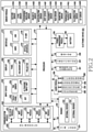
- FIG. 2 is a block diagram of an electronic device according to an embodiment of the present disclosure.
- an electronic device 201 may, for example, include the entire or part of the electronic device 101 illustrated in FIG. 1 .
- the electronic device 201 may include one or more processors (e.g., application processor (APs)) 210, a magnetic field module 220, a subscriber identification module 224, a memory 230, a sensor module 240, an input device 250, a display 260, an interface 270, an audio module 280, a camera module 291, a power management module 295, a battery 296, an indicator 297 and a motor 298.
- APs application processor
- the processor 210 may, for example, drive an operating system or an application program to control a majority of hardware or software constituent elements coupled to the processor 210, and may perform various data processing and operations.
- the processor 210 may be, for example, implemented as a system on chip (SoC).
- SoC system on chip
- the processor 210 may further include a graphic processing unit (GPU) and/or an image signal processor (ISP).
- the processor 210 may include at least some (e.g., cellular module 221) of the constituent elements illustrated in FIG. 2 as well.
- the processor 210 may load a command or data received from at least one of the other constituent elements (e.g., non-volatile memory), to a volatile memory, to process the loaded command or data, and store the result data in the non-volatile memory.
- the magnetic field module 220 may, for example, have the same or similar construction with the communication interface 170.
- the magnetic field module 220 may, for example, include a cellular module 221, a WiFi module 223, a Bluetooth module 225, a GNSS module 227, a near field communication (NFC) module 228, and a radio frequency (RF) module 229.
- the cellular module 221 may, for example, provide voice telephony, video telephony, a text service, an Internet service or the like through a telecommunication network.
- the cellular module 221 may perform the distinction and authentication of the electronic device 201 within the telecommunication network, by using the subscriber identification module (e.g., SIM card) 224.
- SIM card subscriber identification module
- the cellular module 221 may perform at least some functions among functions that the processor 210 may provide.
- the cellular module 221 may include a communication processor (CP).
- CP communication processor
- at least some (e.g., two or more) of the cellular module 221, the WiFi module 223, the Bluetooth module 225, the GNSS module 227 or the NFC module 228 may be included within one integrated chip (IC) or IC package.
- the RF module 229 may, for example, transceive a communication signal (e.g., RF signal).
- the RF module 229 may, for example, include a transceiver, a power amplifier module (PAM), a frequency filter, a low noise amplifier (LNA), an antenna or the like.
- PAM power amplifier module
- LNA low noise amplifier
- the cellular module 221, the WiFi module 223, the Bluetooth module 225, the GNSS module 227 or the NFC module 228 may transceive an RF signal through a separate RF module.
- the subscriber identification module 224 may, for example, include a card including a subscriber identification module and/or an embedded SIM. And, the subscriber identification module 224 may include unique identification information (e.g., integrated circuit card identifier (ICCID)) or subscriber information (e.g., international mobile subscriber identity (IMSI)).
- ICCID integrated circuit card identifier
- IMSI international mobile subscriber identity
- the memory 230 may, for example, include an internal memory 232 or an external memory 234.
- the internal memory 232 may, for example, include at least one of a volatile memory (e.g., a dynamic random access memory (DRAM), a static RAM (SRAM), a synchronous dynamic RAM (SDRAM) or the like) and a non-volatile memory (e.g., one time programmable read only memory (OTPROM), a programmable ROM (PROM), an erasable PROM (EPROM), an electrically EPROM (EEPROM), a mask ROM, a flash ROM, a flash memory, a hard drive or a solid state drive (SSD)).
- a volatile memory e.g., a dynamic random access memory (DRAM), a static RAM (SRAM), a synchronous dynamic RAM (SDRAM) or the like
- a non-volatile memory e.g., one time programmable read only memory (OTPROM), a programmable ROM (PROM),
- the external memory 234 may include a flash drive, for example, a compact flash (CF), a secure digital (SD), a micro-SD, a mini-SD, an extreme Digital (xD), a Multi Media Card (MMC), a memory stick or the like.
- the external memory 234 may be operatively or physically coupled with the electronic device 201 through various interfaces.
- the sensor module 240 may, for example, measure a physical quantity or sense an activation state of the electronic device 201, to convert measured or sensed information into an electrical signal.
- the sensor module 240 may, for example, include at least one of a gesture sensor 240A, a gyro sensor 240B, a barometer 240C, a magnetic sensor 240D, an acceleration sensor 240E, a grip sensor 240F, a proximity sensor 240G, a color sensor 240H (e.g., a red, green, blue (RGB) sensor), a medical sensor 2401, a temperature/humidity sensor 240J, an illuminance sensor 240K or an ultra violet (UV) sensor 240M.
- a gesture sensor 240A e.g., a gyro sensor 240B, a barometer 240C, a magnetic sensor 240D, an acceleration sensor 240E, a grip sensor 240F, a proximity sensor 240G, a color sensor
- the sensor module 240 may, for example, include an E-nose sensor, an electromyography (EMG) sensor, an electroencephalogram (EEG) sensor, an electrocardiogram (ECG) sensor, an infrared (IR) sensor, an iris scan sensor and/or a finger scan sensor.
- the sensor module 240 may further include a control circuit for controlling at least one or more sensors belonging therein.
- the electronic device 201 may further include a processor configured to control the sensor module 240 as a part of the processor 210 or separately, thereby controlling the sensor module 240 while the processor 210 is in a sleep state.
- the input device 250 may, for example, include a touch panel 252, a (digital) pen sensor 254, a key 256 or an ultrasonic input device 258.
- the touch panel 252 may, for example, use at least one scheme among a capacitive overlay scheme, a pressure sensitive scheme, an infrared beam scheme or an ultrasonic scheme.
- the touch panel 252 may further include a control circuit as well.
- the touch panel 252 may further include a tactile layer, to provide a tactile response to a user.
- the (digital) pen sensor 254 may, for example, be a part of the touch panel 252, or include a separate sheet for recognition.
- the key 256 may, for example, include a physical button, an optical key or a keypad.
- the ultrasonic input device 258 may sense an ultrasonic wave generated in an input tool, through a microphone (e.g., microphone 288), to confirm data corresponding to the sensed ultrasonic wave.
- the display 260 may include a panel 262, a hologram device 264, a projector 266, and/or a control circuit for controlling them.
- the panel 262 may, for example, be implemented to be flexible, transparent, or wearable.
- the panel 262 may be constructed as one or more modules together with the touch panel 252.
- the hologram device 264 may show a three-dimensional image to the air using an interference of light.
- the projector 266 may project light onto a screen, to display an image.
- the screen may, for example, be located inside or outside the electronic device 201.
- the interface 270 may, for example, include an HDMI 272, a USB 274, an optical interface 276 or a D-subminiature (D-sub) 278.
- the interface 270 may, for example, be included in the communication interface 170 illustrated in FIG. 1 . Additionally or alternatively, the interface 270 may, for example, include a Mobile High-definition Link (MHL) interface, an SD card / Multi Media Card (MMC) interface or an Infrared Data Association (IrDA) standard interface.
- MHL Mobile High-definition Link
- MMC Multi Media Card
- IrDA Infrared Data Association
- the audio module 280 may, for example, convert a sound and an electrical signal interactively. At least some constituent elements of the audio module 280 may be, for example, included in the input output interface 150 illustrated in FIG. 1 .
- the audio module 280 may for example, process sound information that is inputted or outputted through a speaker 282, a receiver 284, an earphone 286, the microphone 288 or the like.
- the camera module 291 is, for example, a device able to photograph a still image and a video. According to an embodiment, the camera module 291 may include one or more image sensors (e.g., front sensor or rear sensor), a lens, an image signal processor (ISP) or a flash (e.g., an LED, a xenon lamp or the like).
- ISP image signal processor
- flash e.g., an LED, a xenon lamp or the like.
- the power management module 295 may, for example, manage the electric power of the electronic device 201.
- the power management module 295 may include a power management integrated circuit (PMIC), a charger IC or a battery or fuel gauge.
- the PMIC may, for example, employ a wired and/or wireless charging scheme.
- the wireless charging scheme may, for example, include a magnetic resonance scheme, a magnetic induction scheme, an electromagnetic wave scheme or the like.
- the wireless charging scheme may further include a supplementary circuit for wireless charging, for example, a coil loop, a resonance circuit, a rectifier or the like.
- the battery gauge may, for example, measure a level of the battery 296, a voltage being in charge, an electric current or a temperature.
- the battery 296 may, for example, include a rechargeable battery and/or a solar battery.
- the indicator 297 may display a specific state, for example, a booting state, a message state, a charging state or the like of the electronic device 201 or a part (e.g., processor 210) of the electronic device 201.
- the motor 298 may convert an electrical signal into a mechanical vibration, and may generate a vibration, a haptic effect or the like.
- the electronic device 201 may, for example, include a mobile TV support device (e.g., GPU) capable of processing media data according to the standards of digital multimedia broadcasting (DMB), digital video broadcasting (DVB), mediaFlo TM or the like.
- DMB digital multimedia broadcasting
- DVD digital video broadcasting
- mediaFlo TM mediaFlo TM
- Each of the constituent elements described in the present document may consist of one or more components, and a name of the corresponding constituent element may be varied according to the kind of the electronic device.
- the electronic device e.g., electronic device 201) may omit some constituent elements, or further include additional constituent elements, or combine some of
- FIG. 3 is a block diagram of a program module according to an embodiment of the present disclosure.
- a program module 310 e.g., the program 140
- the operating system may, for example, include Android TM , iOS TM , Windows TM , Symbian TM , Tizen TM or Bada TM .
- FIG. 3 is a block diagram of a program module according to an embodiment of the present disclosure.
- a program module 310 may include an Operating System (OS) for controlling resources related to an electronic device (e.g., the electronic device 101) and/or various applications (e.g., the application program 147) driven on the operating system.
- the operating system may, for example, include Android TM , iOS TM , Windows TM , Symbian TM , Tizen TM or Bada
- the program module 310 may include a kernel 320 (e.g., the kernel 141), a middleware 330 (e.g., the middleware 143), an API 360 (e.g., the API 145), and/or an application 370 (e.g., the application program 147). At least a part of the program module 310 may be preloaded onto an electronic device, or be downloaded from an external electronic device (e.g., the electronic device 102, 104, the server 106, etc.).
- a kernel 320 e.g., the kernel 141
- a middleware 330 e.g., the middleware 143
- an API 360 e.g., the API 145
- an application 370 e.g., the application program 147
- the kernel 320 may, for example, include a system resource manager 321 and/or a device driver 323.
- the system resource manager 321 may perform control of a system resource, allocation thereof, recovery thereof or the like.
- the system resource manager 321 may include a process management unit, a memory management unit or a file system management unit.
- the device driver 323 may, for example, include a display driver, a camera driver, a Bluetooth driver, a shared memory driver, a USB driver, a keypad driver, a WiFi driver, an audio driver or an inter-process communication (IPC) driver.
- IPC inter-process communication
- the middleware 330 may, for example, provide a function that the application 370 commonly needs, or provide various functions to the application 370 through the API 360 so that the application 370 may make use of restricted system resources within an electronic device.
- the middleware 330 may include at least one of a runtime library 335, an application manager 341, a window manager 342, a multimedia manager 343, a resource manager 344, a power manager 345, a database manager 346, a package manager 347, a connectivity manager 348, a notification manager 349, a location manager 350, a graphic manager 351 or a security manager 352.
- the runtime library 335 may, for example, include a library module that a compiler uses to add a new function through a programming language while the application 370 is executed.
- the runtime library 335 may perform input output management, memory management or arithmetic function processing.
- the application manager 341 may, for example, manage a lifecycle of the application 370.
- the window manager 342 may manage a graphic user interface (GUI) resource used by a screen.
- the multimedia manager 343 may detect a format required for playing media files, and perform encoding or decoding of the media file by using a codec suitable to the corresponding format.
- the resource manager 344 may manage a source code of the application 370 or a space of a memory.
- the power manager 345 may, for example, manage a battery capacity or a power supply, and provide power information required for an operation of an electronic device. According to an embodiment, the power manager 345 may interwork with a basic input/output system (BIOS).
- the database manager 346 may, for example, create, search or change a database that will be used by the application 370.
- the package manager 347 may manage installation or updating of an application that is distributed in a form of a package file.
- the connectivity manager 348 may, for example, manage wireless connectivity.
- the notification manager 349 may, for example, provide events such as an arrival message, an appointment, a proximity notification, etc. to a user.
- the location manager 350 may, for example, manage location information of an electronic device.
- the graphic manager 351 may, for example, manage a graphic effect that will be provided to a user, or a user interface related with this.
- the security manager 352 may, for example, provide system security or user authentication.
- the middleware 330 may include a telephony manager for managing a voice or video telephony function of an electronic device, or a middleware module capable of forming a combination of functions of the aforementioned constituent elements.
- the middleware 330 may provide a module that is specialized based on the type of an operating system.
- the middleware 330 may dynamically delete some of the existing constituent elements or add new constituent elements.
- the API 360 is, for example, a set of API programming functions, and may be provided to have another construction in accordance with the operating system.
- Android or iOS may provide one API set by platform
- Tizen may provide two or more API sets by platform.
- the application 370 may, for example, include a home 371, a dialer 372, a short message service (SMS) / multimedia messaging service (MMS) 373, an instant message (IM) 374, a browser 375, a camera 376, an alarm 377, a contact 378, a voice dial 379, an electronic mail (e-mail) 380, a calendar 381, a media player 382, an album 383, a watch 384, health care (e.g., measuring a momentum, a blood sugar or the like), or an environment information (e.g., air pressure, humidity or temperature information) provision application.
- the application 370 may include an information exchange application that may support information exchange between an electronic device and an external electronic device.
- the information exchange application may, for example, include a notification relay application for relaying specific information to the external electronic device, or a device management application for managing the external electronic device.
- the notification relay application may relay notification information generated by another application of an electronic device to an external electronic device, or receive notification information from the external electronic device to provide the received notification information to a user.
- the device management application may, for example, install, delete or update a function (e.g., turn-on / turn-off of the external electronic device itself (or some constituent components) or adjustment of a brightness (or resolution) of a display) of the external electronic device that communicates with the electronic device, or an application operating in the external electronic device.
- the application 370 may include an application (e.g., a health care application of a mobile medical instrument) designated according to an attribute of the external electronic device.
- the application 370 may include an application received from the external electronic device.
- At least a part of the program module 310 may be implemented (e.g., executed) by software, firmware, hardware (e.g., the processor 210) or a combination of at least two or more of them, and may include a module for performing one or more functions, a program, a routine, sets of instructions or a process.
- module may include a unit consisting of hardware, software, or firmware, and may, for example, be used interchangeably with the term “logic”, “logical block”, “component”, “circuit”, or the like.
- the “module” may be an integrated component, or a minimum unit for performing one or more functions or a part thereof.
- the “module” may be mechanically or electronically implemented and may include, for example, an Application-Specific Integrated Circuit (ASIC) chip, a Field-Programmable Gate Arrays (FPGA), or a programmable-logic device, which has been known or are to be developed in the future, for performing certain operations.
- ASIC Application-Specific Integrated Circuit
- FPGA Field-Programmable Gate Arrays
- At least some of devices (e.g., modules or functions thereof) or methods (e.g., operations) may be implemented by an instruction which is stored a computer-readable storage medium (e.g., the memory 130) in the form of a program module.
- the instruction when executed by a processor (e.g., the processor 120), may cause the one or more processors to execute the function corresponding to the instruction.
- the computer-readable storage medium may include a hard disk, a floppy disk, a magnetic medium (e.g., a magnetic tape), an Optical Media (e.g., CD-ROM, DVD), a Magneto-Optical Media (e.g., a floptical disk), an inner memory, etc.
- the instruction may include a code made by a complier or a code that can be executed by an interpreter.
- the programming module may include one or more of the aforementioned components or may further include other additional components, or some of the aforementioned components may be omitted. Operations performed by a module, a programming module, or other elements according to various embodiments may be executed sequentially, in parallel, repeatedly, or in a heuristic manner. At least some operations may be executed according to another sequence, may be omitted, or may further include other operations.
- FIG. 4 is a block diagram of an electronic device 400 according to various embodiments.
- the electronic device 400 may include an input unit 410, a display unit 420, a sensor unit 430, a communication unit 440, a charging unit 450, a storing unit 460, and a control unit 470.
- the input unit 410 may generate input data in the electronic device 400. In this case, the input unit 410 may generate the input data in response to a user input of the electronic device 400. In addition, the input unit 410 may include at least one input means.
- the input unit 410 may include a key pad, a dome switch, a physical button, a touch panel, and a jog & shuttle.
- the display unit 420 may output display data in the electronic device 400.
- the display unit 420 may be implemented as a touch screen by being coupled to the input unit 410.
- the display unit 420 may include a Liquid Crystal Display (LCD), a Light Emitting Diode (LED) display, an Organic Light-Emitting Diode (OLED) display, a Micro Electro Mechanical System (MEMS) display, and an electronic paper display.
- LCD Liquid Crystal Display
- LED Light Emitting Diode
- OLED Organic Light-Emitting Diode
- MEMS Micro Electro Mechanical System
- the sensor unit 430 may detect at least any one of a status of the electronic device 400 and a peripheral status of the electronic device 400.
- the sensor unit 430 may include at least one sensor.
- the sensor unit 430 may include a fingerprint sensor to detect a fingerprint of a user of the electronic device 400.
- the fingerprint sensor may be coupled to the input unit 410 of the electronic device 400.
- the fingerprint sensor 141 may include an optical fingerprint sensor which captures the fingerprint of the user of the electronic device 400 as an image, an ultrasonic fingerprint sensor, a capacitive fingerprint sensor, a semiconductor-type fingerprint sensor which detects electric conductivity, and a heart rate sensor.
- the communication unit 440 may perform communication in the electronic device 400.
- the communication unit 440 may communicate with an external device (not shown) by using various communication schemes.
- the communication unit 440 may perform communication in a wired or wireless manner.
- the external electronic device may include, for example, an electronic device, a base station, a server, and a satellite.
- communication schemes may include at least any one of a cellular communication scheme, a short range communication scheme, and a wireless charging scheme.
- the cellular communication scheme may include, for example, a Long Term Evolution (LTE) scheme, a Wideband Code Division Multiple Access (WCDMA) scheme, and a Global System for Mobile communications (GSM) scheme.
- the short range communication scheme may include, for example, a Wireless Fidelity (WiFi) scheme, a wireless Local Area Network (LNA) scheme, a Bluetooth scheme, a Near Field Communications (NFC) scheme, and a Magnetic Secure Transmission (MST) scheme.
- the wireless charging scheme may include, for example, a magnetic resonance scheme, an electromagnetic induction scheme, and a Radio Frequency (RF)/micro wave radiation scheme.
- RF Radio Frequency
- the charging unit 450 may store power in the electronic device 400. In addition, the charging unit 450 may supply the power to drive the electronic device 400. For this, the charging unit 450 may perform charging and discharging repetitively.
- the storing unit 460 may store operating programs of the electronic device 400. According to various embodiments, the storing unit 460 may store programs for performing communication by using various communication schemes. In addition, the storing unit 460 may store data generated during the programs are executed.
- the control unit 470 may provide an overall control to the electronic device 400. In this case, the control unit 470 may perform various functions. For this, the control unit 470 may control components of the electronic device 400. In addition, the control unit 470 may receive and process a command or data from the components of the electronic device 400.
- FIG. 5A and FIG. 5B illustrate block diagrams of a magnetic field communication and charging unit of the communication unit 440 in the electronic device 400 according to various embodiments.
- the magnetic field communication and charging unit of the communication unit 440 includes a first antenna 510, a second antenna 520, a third antenna 530, a first magnetic field module 540, a second magnetic field module 550, a first connection unit 570, and a second connection unit 580.
- the first antenna 510 may be driven in response to a high frequency band f 1 .
- the first antenna 510 may be commonly used based on a plurality of magnetic field schemes.
- the high frequency band f 1 may support a first short range communication scheme and a first charging scheme.
- the first short range communication scheme may be an NFC scheme
- the first charging scheme may be a magnetic resonance scheme.
- the high frequency band f 1 may include a first high frequency band f 11 for the magnetic resonance scheme and a second high frequency band f 12 for the NFC.
- the first high frequency band f 11 and at least part of the second high frequency band f 12 may overlap with each other in a frequency domain, and the first high frequency band f 11 and the second high frequency band f 12 may be separated from each other in the frequency domain.
- the second high frequency band f 12 may correspond to a multiplication of the first frequency band f 11 (i.e., n ⁇ f 11 ).
- the second antenna 520 may be driven independently. In this case, the second antenna 520 may be driven in response to a first low frequency band f 21 . In addition, the second antenna 520 and the third antenna 530 may be coupled to be driven together. In this case, the second antenna 520 and the third antenna 530 may be driven in response to a second low frequency band f 22 .
- the second antenna 520 may be commonly used based on a plurality of magnetic field communication and charging schemes.
- the first low frequency band f 21 may support a second charging scheme
- the second low frequency band f 22 may support a second short range communication scheme.
- the second charging scheme may be an electromagnetic induction scheme
- the second short range communication scheme may be an MST scheme.
- At least part of the first low frequency band f 21 and at least part of the second low frequency band f 22 may overlap with each other in the frequency domain, and the first low frequency band f 21 and the second low frequency band f 22 may be separated from each other in the frequency domain.
- the first magnetic field module 540 may perform communication by using the first antenna 510. According to various embodiments, the first magnetic field module 540 may use the first antenna 510 according to the first short range communication scheme. Accordingly, the first magnetic field module 540 may perform first short range communication through the first antenna 510. In this case, the first magnetic field module 540 may perform first short range communication through the high frequency band f 1 . According to an embodiment, the first short range communication scheme may be an NFC scheme. For example, the first magnetic field module 540 may perform the NFC through the second high frequency band f 12 .
- the second magnetic field module 550 may perform communication by using at least any one of the first antenna 510, the second antenna 520, and the third antenna 530. According to various embodiments, the second magnetic field module 550 receives power wirelessly by using any one of the first antenna 510 and the second antenna 520. According to various embodiments, the second magnetic field module 550 performs second short range communication by using the third antenna 530.
- the second magnetic field module uses the first antenna 510 on the basis of the first charging scheme, and uses the second antenna 520 on the basis of the second charging scheme. Accordingly, the second magnetic field module 550 receives power through the first antenna 510 by using the first charging scheme, and receives power through the second antenna 520 by using the second charging scheme.
- the first charging scheme may be a magnetic resonance scheme
- the second charging scheme may be an electromagnetic induction scheme.
- the second magnetic field module 550 may receive power through the first high frequency band f 11 by using the magnetic resonance scheme, and may receive power through the first low frequency band f 21 by using the electromagnetic induction scheme.
- the second magnetic field module 550 uses the second antenna 520 and the third antenna 530 on the basis of the second short range communication scheme. Accordingly, the second magnetic field module 550 performs second short range communication through the second antenna 520 and the third antenna 530.
- the second short range communication scheme may be a Magnetic Secure Transmission (MST) scheme.
- MST Magnetic Secure Transmission
- the second magnetic field module 550 may perform MST through the second frequency band f 22 .
- An MST technique is a communication technique for an offline payment using a magnetic field, and may be used to perform communication with a Point of Sale (POS) device.
- POS Point of Sale
- the second magnetic field module 550 includes a first circuit unit 551 and a second circuit unit 553.
- the first circuit unit 551 receives power through the first antenna 510 by using the first charging scheme, and receives power through the second antenna 520 by using the second charging scheme.
- the second circuit unit 553 performs second short range communication through the second antenna 520 and the third antenna 530.
- the first connection unit 570 controls a connection between the first antenna 510 and the first magnetic field module 540.
- the first connection unit 570 may be disposed between the first antenna 510 and the first magnetic field module 540.
- the first connection unit 570 may operate under the control of the control unit 470.
- the first connection unit 570 operates based on driving of the first magnetic field module 540. For example, when the first magnetic field module 540 is not driven, the first connection unit 570 releases the connection between the first antenna 510 and the first magnetic field module 540. Meanwhile, when the first magnetic field module 540 is driven, the first connection unit 570 couples the first antenna 510 and the first magnetic field module 540. Accordingly, when the first magnetic field module 540 is not driven, the first connection unit 570 may separate the first magnetic field module 540 to protect it.
- the second connection unit 580 controls a connection between the second antenna 520, the third antenna 530, and the second magnetic field module 550.
- the second connection unit may be disposed between the second antenna 520 and the second magnetic field module 550 and between the third antenna 530 and the second magnetic field module 550.
- the second connection unit 580 may operate under the control of the controller 470.
- the second connection unit 580 operates based on driving of the second magnetic field module 550. For example, when the second magnetic field module 550 is not driven, the second connection unit 580 releases the connection between the third antenna 530 and the second magnetic field module 550.
- the second connection unit 580 couples the third antenna 530 and the second magnetic field module 550. Accordingly, when the second magnetic field module 550 is not driven, the second connection unit 580 may separate the second magnetic field module 550 to protect it.
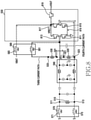
- FIG. 6 illustrates a circuit diagram of a magnetic field communication and charging unit of the communication unit 440 in the electronic device 400 according to various embodiments.
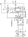
- FIG. 7 , FIG. 8 , and FIG. 9 illustrate circuit diagrams of the second magnetic field module 550 of FIG. 6 .
- the magnetic field communication and charging unit of the communication unit 440 may include a first antenna 510, a second antenna 520, a third antenna 530, a first magnetic field module 540, a second magnetic field module 550, a first connection unit 570, and a second connection unit 580.
- the first antenna 510 may be coupled to the first magnetic field module 540 and the second magnetic field module 550.
- the first antenna 510 may include a first terminal 511 and a second terminal 513. That is, the first terminal 511 and the second terminal 513 may be disposed at both end portions in the first antenna 510.
- the first terminal 511 may be coupled to the first magnetic field module 540 and the second magnetic field module 550
- the second terminal 513 may be coupled to the first magnetic field module 540 and the second magnetic field module 550.
- the first terminal 511 and the second terminal 513 may not be directly coupled to the first magnetic field module 540, but may be coupled to the first magnetic field module 540 through the first connection unit 570.
- the first terminal 511 and the second terminal 513 may be coupled to the first connection unit 570 and the second magnetic field module 550.
- the first antenna 510 may be represented by a first inductor L1.
- the first antenna 510 may be represented by a first capacitor C1 together with the first inductor L1.
- the first capacitor C1 may be coupled in parallel to the first inductor LI, between the first antenna 510 and the second magnetic field module 550.
- the first capacitor C1 may be provided for frequency matching between the first antenna 510 and the second magnetic field module 550.
- capacitance of the first capacitor C1 may be determined according to inductance of the first inductor L1 and the first high frequency band f 11 as shown in Equation (1) below.
- C 1 1 2 ⁇ f 11 2 ⁇ L 1
- the second antenna 520 may be coupled to the second magnetic field module 550.
- the second antenna 520 may include a first terminal 521 and a second terminal 523. That is, the first terminal 521 and the second terminal 523 may be disposed at both end portions of the second antenna 520.
- the first terminal 521 and the second terminal 523 may be coupled to the second magnetic field module 550.
- the second antenna 520 may be coupled in parallel to the first antenna 510.
- the second antenna 520 may be represented by a second inductor L2.
- the second antenna 520 may be represented by a second capacitor C2 together with the second inductor L2.
- the second capacitor C2 may be coupled in series to the second inductor L2, between the second antenna 520 and the second magnetic field module 550.
- the second capacitor C2 may be provided for frequency matching between the second antenna 520 and the second magnetic field module 550.
- capacitance of the second capacitor C2 may be determined according to inductance of the second inductor L2 and the first low frequency band f 21 as shown in Equation (2) below.
- C 2 1 2 ⁇ f 21 2 ⁇ L 2
- the third antenna 530 may be coupled to the second magnetic field module 550.
- the third antenna 530 may be coupled to the second antenna 520.
- the third antenna 530 may include a connecting terminal 531 and a third terminal 533. That is, the connecting terminal 531 and the third terminal 533 may be disposed at both end portions of the third antenna 530.
- the connecting terminal 531 may be coupled to the second antenna 520, and the third terminal 533 may be coupled to the second magnetic field module 550.
- the third terminal 533 may not be directly coupled to the second magnetic field module 550, but may be coupled to the second magnetic field module 550 through the second connection unit 580.
- the third antenna 530 may be coupled in parallel to the first antenna 510, and may be coupled in series to the second antenna 520.
- the third antenna 530 may be represented by a third inductor L3.
- the first magnetic field module 540 may be coupled to the first antenna 510.
- the first magnetic field module 540 may be coupled to the first terminal 511 and second terminal 513 of the first antenna 510.
- the first magnetic field module 540 may not be directly coupled to the first terminal 511 and the second terminal 513, but may be coupled to the first terminal 511 and the second terminal 513 through the first connection unit 507. Accordingly, the first magnetic field module 540 may perform NFC through the second high frequency band f 12 on the basis of the inductance of the first inductor L1.
- the first magnetic field module 540 may include a matching circuit unit 541.
- the matching circuit unit 541 may be disposed inside the first magnetic field module 540, and thus the first magnetic field module 540 and the matching circuit unit 541 may be constructed integrally.
- the matching circuit unit 541 may be disposed outside the first magnetic field module 540, and thus the first magnetic field module 540 and the matching circuit unit 541 may be constructed independently from each other.
- the matching circuit unit 541 may be disposed between the first antenna 510 and the first magnetic field module 540.
- the matching circuit unit 541 may be disposed between the first connection unit 570 and the first magnetic field module 540.
- the matching circuit unit 541 may be provided for frequency matching between the first antenna 510 and the first magnetic field module 540.
- capacitance of the matching circuit unit 541 may be determined according to the inductance of the first inductor L1 and the capacitance of the first capacitor C1.
- the second magnetic field module 550 may be coupled to the first antenna 510, the second antenna 520, and the third antenna 530.
- the second magnetic field module 550 may be coupled to the first terminal 511 and second terminal 513 of the first antenna 510. Accordingly, the second magnetic field module 550 may receive power through the first frequency band f 11 by using the magnetic resonance scheme on the basis of a combination of the inductance of the first inductor L1 and the capacitance of the first capacitor C1.
- the second magnetic field module 550 may be coupled to the first terminal 521 and second terminal 523 of the second antenna 520.
- the second magnetic field module 550 may receive power by using the electromagnetic induction scheme through the first frequency band f 21 on the basis of the inductance of the second inductor L2 and the capacitance of the second capacitor C2. Further, the second magnetic field module 550 may be coupled to the second terminal 523 of the second antenna 520 and the third terminal 533 of the third antenna 530. Accordingly, the second magnetic field module 550 may perform MST through the second low frequency band f 22 on the basis of a combination of the inductance of the second inductor L2 and the inductance of the third inductor L3.
- the first connection unit 570 may be coupled to the first antenna 510 and the first magnetic field module 540.
- the first connection unit 570 may include one or more switches 571 and 573, for example, the input switch 571 and the output switch 573.
- the input switch 571 may be disposed between the first terminal 511 of the first antenna 510 and the first magnetic field module 540.
- the output switch 573 may be disposed between the second terminal 513 of the first antenna 510 and the first magnetic field module 540.
- a first current path may be provided along the first magnetic field module 540, the input switch 571, the first terminal 511 of the first antenna 510, the first antenna 510, the second terminal 513 of the first antenna 510, the output switch 573, and the first magnetic field module 540.
- a second current path may be provided along the second magnetic field module 550, the first terminal 511 of the first antenna 510, the first antenna 510, the second terminal 513 of the first antenna 510, and the second magnetic field module 550.
- the second connection unit 580 may be coupled to the third antenna 530 and the second magnetic field module 550.
- the second connection unit 580 may include one or more switches 581 and 583, for example, the first connection switch 581 and the second connection switch 583.
- the first connection switch 581 may be disposed between the first terminal 521 of the second antenna 520 and the second magnetic field module 550.
- the second connection switch 583 may be disposed between the third antenna 530 and the second magnetic field module 550.
- a third current path may be provided along the second magnetic field module 550, the second terminal 523 of the second antenna 520, the second antenna 520, the connecting portion 531 of the third antenna 530, the third antenna 530, the third terminal 533 of the third antenna 530, and the second magnetic field module 550.
- a fourth current path may be provided along the second magnetic field module 550, the first terminal 521 of the second antenna 520, the second antenna 520, the second terminal 523 of the second antenna 520, and the second magnetic field module 550.
- the communication unit 440 may further include a noise reducing filter 590.
- the noise reducing filter 590 may be disposed between the first magnetic field module 540 and the second magnetic field module 550.
- the noise reducing filter 590 may suppress a noise input from the first magnetic field module 540 to the second magnetic field module 550, in response to driving of the first magnetic field module 540.
- the noise reducing filter 590 may suppress a noise input from the second magnetic field module 550 to the first magnetic field module 540, in response to driving of the second magnetic field module 550.
- the second magnetic field module 550 may include a first circuit unit 710 and a second circuit unit 720.
- the first circuit unit 710 may be coupled to the first antenna 510 and the second antenna 520.
- the first circuit unit 710 may be coupled to the first terminal 511 and second terminal 513 of the first antenna 510 and a first terminal 521 and second terminal 523 of the second antenna 520.
- the first circuit unit 710 may receive power through the first frequency band f 11 by using the magnetic resonance scheme on the basis of a combination of the inductance of the first inductor L1 and the capacitance of the first capacitor C1.
- the first circuit unit 710 may receive power by using the electromagnetic induction scheme through the first frequency band f 21 on the basis of the inductance of the second inductor L2 and the capacitance of the second capacitor C2.
- the first circuit unit 710 may include an inverter.
- the first circuit unit 710 may include a first switch 711, second switch 713, third switch 715, and fourth switch 717 arranged in a bridge form and a status switch 719.
- the first switch 711 and the third switch 715 may be commonly grounded.
- the second switch 713 and the fourth switch 717 may be coupled to the status switch 719.
- the first switch 711 and the second switch 713 may be coupled in series, and the third switch 715 and the fourth switch 717 may be coupled in series.
- the first and second switches 711 and 713 and the third and fourth switches 715 and 717 may be coupled in parallel to each other.
- the first terminal 511 of the first antenna 510 may be coupled, and the first terminal 521 of the second antenna 520 may be coupled through the second capacitor C2.
- the second terminal 513 of the first antenna 510 may be coupled, and the second terminal 523 of the second antenna 520 may be coupled.
- the status switch 719 may be coupled to the fourth switch 717 and the charging unit 450. Accordingly, a second current path may be provided along the first terminal 511, the first antenna 510, the second terminal 513, the fourth switch 717, and the status switch 719. Meanwhile, a fourth current path may be provided along the first terminal 521, the second antenna 520, the second terminal 523, the fourth switch 717, and the status switch 719.
- the second circuit unit 720 may be coupled to the second antenna 520 and the third antenna 530 through the second connection unit 580.
- the second circuit unit 720 may be coupled to the first terminal 521 of the second antenna 520 through the first connection switch 581, and may be coupled to the third terminal 533 of the third antenna 530 through the second connection switch 583.
- the second circuit unit 720 may perform MST through the second low frequency band f 22 on the basis of a combination of the inductance of the second inductor L2 and the inductance of the third inductor L3.
- the second circuit unit 720 may include an inverter.
- the second circuit unit 720 may include a first switch 721, second switch 723, third switch 725, and fourth switch 727 which are arranged in a bridge form.
- the first switch 721 and the third switch 725 may be coupled to the charging unit 450 or the control unit 470.
- a source of the second switch 723 and a source of the fourth switch 727 may be commonly grounded.
- the first switch 721 and the second switch 723 may be coupled in series, and the third switch 725 and the fourth switch 727 may be coupled in series.
- the first and second switches 721 and 723 and the third and fourth switches 725 and 727 may be coupled in parallel to each other.
- the first terminal 521 of the second antenna 520 may be coupled through the first connection switch 581 of the second connection unit 580.
- the third terminal 533 of the third antenna 530 may be coupled through the second connection switch 583 of the second connection unit 580. Accordingly, a third current path may be provided along the charging unit 450 or the control unit 470, the first switch 721, the first connection switch 581, the second terminal 523, the second antenna 510, the connecting terminal 531, the third antenna 530, the third terminal 533, the second connection switch 583, and the fourth switch 717.
- the second magnetic field module 550 may include an integrated circuit unit 810.
- the integrated circuit unit 810 may be coupled to the first antenna 510 and the second antenna 520.
- the integrated circuit unit 810 may be coupled to the first terminal 511 and second terminal 513 of the first antenna 510 and the first terminal 521 and second terminal 523 of the second antenna 520.
- the integrated circuit unit 810 may receive power through the first frequency band f 11 by using the magnetic resonance scheme on the basis of a combination of the inductance of the first inductor L1 and the capacitance of the first capacitor C1.
- the integrated circuit unit 810 may receive power by using the electromagnetic induction scheme through the first frequency band f 21 on the basis of the inductance of the second inductor L2 and the capacitance of the second capacitor C2.
- the integrated circuit unit 810 may be coupled to the third antenna 530 through the second connection unit 580.
- the integrated circuit unit 810 may be coupled to the third terminal 533 of the third antenna 530 through the first connection switch 581. Accordingly, the integrated circuit unit 810 may perform MST through the second low frequency band f 22 on the basis of a combination of the inductance of the second inductor L2 and the inductance of the third inductor L3.
- the integrated circuit unit 810 may include an inverter.
- the integrated circuit unit 810 may include a first switch 811, second switch 813, third switch 815, and fourth switch 817 arranged in a bridge form and a status switch 819.
- the first switch 811 and the third switch 815 may be commonly grounded.
- the first switch 811 and the second switch 813 may be coupled in series, and the third switch 815 and the fourth switch 817 may be coupled in series.
- the first and second switches 811 and 813 and the third and fourth switches 815 and 817 may be coupled in parallel to each other.
- the first terminal 511 of the first antenna 510 may be coupled, and the first terminal 521 of the second antenna 520 may be coupled through the second capacitor C2.
- the second terminal 513 of the first antenna 510 may be coupled, and the second terminal 523 of the second antenna 520 may be coupled.
- the second switch 813 and the fourth switch 817 may be coupled to the status switch 819.
- the status switch 819 may be coupled between the second and fourth switches 813 and 817 and the charging unit 450. Accordingly, a second current path may be provided along the first terminal 511, the first antenna 510, the second terminal 513, the fourth switch 817, and the status switch 819. Meanwhile, a fourth current path may be provided along the first terminal 521, the second antenna 520, the second terminal 523, the fourth switch 817, and the status switch 819.
- the third terminal 533 of the third antenna 530 may be coupled through the first connection switch 581 of the second connection unit 580.
- the second terminal 523 of the second antenna 520 may be coupled.
- the second switch 813 and the fourth switch 817 may be coupled to the charging unit 450 or the control unit 470 through the second connection switch 583 of the second connection unit 580. Accordingly, a third current path may be provided along the charging unit 450 or the control unit 470, the second connection switch 583, the second switch 823, the first connection switch 581, the third terminal 533, the third antenna 530, the connecting terminal 531, the second antenna 510, the second terminal 523, and the third switch 815.
- the second magnetic field module 550 may include the second connection unit 580 and an integrated circuit unit 910. That is, the second connection unit 580 may be embedded in the second magnetic field module 550, and thus the second magnetic field module 550 and the second connection unit 580 may be constructed integrally.
- the second connection unit 580 may include the first connection switch 581 and the second connection switch 583.
- the integrated circuit unit 910 may be coupled to the first antenna 510 and the second antenna 520.
- the integrated circuit unit 910 may be coupled to the first terminal 511 and second terminal 513 of the first antenna 510 and the first terminal 521 and second terminal 523 of the second antenna 520.
- the integrated circuit unit 910 may receive power through the first frequency band f 11 by using the magnetic resonance scheme on the basis of a combination of the inductance of the first inductor L1 and the capacitance of the first capacitor C1.
- the integrated circuit unit 910 may receive power by using the electromagnetic induction scheme through the first frequency band f 21 on the basis of the inductance of the second inductor L2 and the capacitance of the second capacitor C2.
- the integrated circuit unit 910 may be coupled to the third antenna 530 through the second connection unit 580.
- the integrated circuit unit 910 may be coupled to the third terminal 533 of the third antenna 530 through the first connection switch 581. Accordingly, the integrated circuit unit 910 may perform MST through the second low frequency band f 22 on the basis of a combination of the inductance of the second inductor L2 and the inductance of the third inductor L3.
- the integrated circuit unit 910 may include an inverter.
- the integrated circuit unit 910 may include a first switch 911, second switch 913, third switch 915, and fourth switch 917 arranged in a bridge form and a status switch 919.
- the first switch 911 and the third switch 915 may be commonly grounded.
- the first switch 911 and the second switch 913 may be coupled in series, and the third switch 915 and the fourth switch 917 may be coupled in series.
- the first and second switches 911 and 913 and the third and fourth switches 915 and 917 may be coupled in parallel to each other.
- the first terminal 511 of the first antenna 510 may be coupled, and the first terminal 521 of the second antenna 520 may be coupled through the second capacitor C2.
- the second terminal 513 of the first antenna 510 may be coupled, and the second terminal 523 of the second antenna 520 may be coupled.
- the second switch 913 and the fourth switch 917 may be coupled to the status switch 919.
- the status switch 919 may be coupled between the second and fourth switches 913 and 917 and the charging unit 450. Accordingly, a second current path may be provided along the first terminal 511, the first antenna 510, the second terminal 513, the fourth switch 917, and the status switch 919. Meanwhile, a fourth current path may be provided along the first terminal 521, the second antenna 520, the second terminal 523, the fourth switch 917, and the status switch 919.
- the third terminal 533 of the third antenna 530 may be coupled through the first connection switch 581 of the second connection unit 580.
- the second terminal 523 of the second antenna 520 may be coupled.
- the second switch 913 and the fourth switch 917 may be coupled to the charging unit 450 or the control unit 470 through the second connection switch 583 of the second connection unit 580. Accordingly, a third current path may be provided along the charging unit 450 or the control unit 470, the second connection switch 583, the second switch 923, the first connection switch 581, the third terminal 533, the third antenna 530, the connecting terminal 531, the second antenna 510, the second terminal 523, and the third switch 915.
- FIG. 10 illustrate perspective views of an electronic device 1000 according to various embodiments.
- FIG. 11 illustrates an exploded view of the electronic device 1000 according to various embodiments.
- the electronic device 1000 according to various embodiments may include at least part of the electronic device 400 of FIG. 4 .
- the electronic device 1000 may include a housing 1010, a front cover 1020, and a rear cover 1030.
- the electronic device 1000 may be provided in a structure in which the housing 1010, the front cover 1020, and the rear cover 1030 are joined. That is, the front cover 1020 may be joined to an upper side of the housing 1010, and the rear cover 1030 may be joined to a lower side of the housing 1010.
- a space may be provided between the housing 1010 and the front cover 1020 and between the housing 1010 and the rear cover 1030.
- the front cover 1020 and the rear cover 1030 may be joined to each other in respective edge regions, and may be joined in a boundary region of the housing 1010. In this case, an accommodation groove 1011 may be disposed to an inner region of the housing 1010.
- the front cover 1020 may be constructed of a transparent material.
- the electronic device 1000 may include an interface module 1110, a support member 1120, a driving board 1130, a battery pack 1140, and an antenna module 1150.
- the interface module 1110, the driving board 1130, the battery pack 1140, and the antenna module 1150 may be electrically coupled. That is, the driving board 1130 may be coupled to each of the interface module 1110, the battery pack 1140, and the antenna module 1150.
- the interface module 1110, the support member 1120, the driving board 1130, and the battery pack 1140 may be mounted between the housing 1010 and the front cover 1020.
- the interface module 1110 may be disposed by facing the front cover 1010.
- the interface module 1110 may include the display unit 420 of FIG. 4 .
- the interface module 1110 may include the input unit 410 and display unit 420 of FIG. 4 .
- the interface module 1110 may be mounted to an upper side of the support member 1120.
- the support member 1120 may fix and support the interface module 1110.
- the driving board 1130 may be mounted to a lower side of the support member 1120.
- the driving board 1130 may include a portion of the communication unit 440 of FIG.
- the driving board 1130 may include the first magnetic field module 540, second magnetic field module 550, first connection unit 570, and second connection unit 580 of FIG. 5 .
- the battery pack 1140 may be disposed in parallel to one side of the driving board 1130.
- the battery pack 1140 may be disposed to a lower side of the driving board 1130. At least part of the battery pack 1140 may be inserted to the accommodation groove 1011 of the housing 1010.
- the battery pack 1140 may include the charging unit 450 of FIG. 4 .
- the antenna module 1150 may be mounted between the housing 1010 and the rear cover 1030.
- the antenna module 1150 may be attached to the driving board 1130.
- the antenna module 1150 may include a portion of the communication unit 440 of FIG. 4 .
- the antenna module 1150 may include the first antenna 510, second antenna 520, and third antenna 530 of FIG. 5 .
- FIG. 12 illustrates a cross-sectional view cut along the line A-A' of an antenna module in an electronic device according to various embodiments.
- FIG. 13 illustrates plan views of an example of an antenna module in an electronic device according to various embodiments.
- FIG. 14 illustrates plan views of another example of an antenna module in an electronic device according to various embodiments.
- the antenna module 1150 may include a first coil 1210, a second coil 1220, a third coil 1230, a mounting member 1240, and a shielding member 1250.
- the first coil 1210 may be driven in response to the high frequency band f 1 .
- the first coil 1210 may be coupled to the driving board 1130.
- the first coil 1210 may include a first terminal 1211 and a second terminal 1213. That is, the first terminal 1211 and the second terminal 1213 may be disposed to both end portions of the first coil 1210.
- the first terminal 1211 and the second terminal 1213 may be coupled to the driving board 1130.
- the first coil 1210 may correspond to the first antenna 510 of FIG. 5 and FIG. 6 .
- the first terminal 1211 and second terminal 1213 of the first coil 1210 may correspond to the first terminal 511 and second terminal 513 of the first antenna 510.
- the first terminal 1211 and second terminal 1213 of the first coil 1210 may be coupled to the first magnetic field module 540 and second magnetic field module 550 of the driving board 1130.
- the first coil 1210 may be commonly used based on a plurality of magnetic field communication and charging schemes.
- the high frequency band f 1 may support a first short range communication scheme and a first charging scheme.
- the first short range communication scheme may be an NFC scheme
- the first charging scheme may be a magnetic resonance scheme.
- the high frequency band f 1 may include the first high frequency band f 11 for the magnetic resonance scheme and the second high frequency band f 12 for the NFC.
- the first frequency band f 11 may correspond to about 6.78 MHz
- the second high frequency band f 12 may correspond to a multiplication of the first frequency band f 11 , i.e., about 13.56 MHz.
- the first coil 1210 may be designed in response to the high frequency band f 1 as shown in Table 1 below. That is, the first coil 1210 may be designed according to the inductance of the first inductor L1 and the capacitance of the first capacitor C1 of FIG. 6 .
- the inductance of the first inductor L1 may correspond to about 1.30 ⁇ H to 1.65 ⁇ H.
- the inductance of the first inductor L1 may be determined according to a size, i.e., an electrical length and thickness, of the first coil 1210.
- the capacitance of the first capacitor C1 may be calculated according to the inductance of the first inductor L1 and the first high frequency band f 11 . In this case, the capacitance of the first capacitor C1 may be determined according to a partial interval in the first coil 1210.
- the second coil 1220 may be driven independently. In this case, a second coil 1220 may be driven in response to the first low frequency band f 21 . In addition, the second coil 1220 and the third coil 1230 may be connected to be driven together. In this case, the second coil 1220 and the third coil 1230 may be driven in response to the second low frequency band f 22 . The second coil 1220 and the third coil 1230 may be coupled to the driving board 1130.
- the second coil 1220 may include the first terminal 1221 and the second terminal 1223. That is, the first terminal 1221 and the second terminal 1223 may be disposed to both end portions of the second coil 1220. In addition, the first terminal 1221 and the second terminal 1223 may be coupled to the driving board 1130. According to various embodiments, the second coil 1220 may correspond to the second antenna 520 of FIG. 5 and FIG. 6 . In this case, the first terminal 1221 and second terminal 1223 of the second coil 1220 may correspond to the first terminal 521 and second terminal 523 of the second antenna 520. Accordingly, the first terminal 1221 and second terminal 1223 of the second coil 1220 may be coupled to the second magnetic field module 550 of the driving board 1130.
- the third coil 1230 may include a connecting terminal 1231 and a third terminal 1233. That is, the connecting terminal 1231 and the third terminal 1233 may be disposed to both end portions of the third coil 1230. In addition, the connecting terminal 1231 and the third terminal 1233 may be coupled to the driving board 1130. According to various embodiments, the third coil 1230 may correspond to the third antenna 530 of FIG. 4 and FIG. 6 . In this case, the connecting terminal 1231 and third terminal 1233 of the third coil 1230 may correspond to the first terminal 531 and third terminal 533 of the third antenna 530. Accordingly, the connecting terminal 1231 of the third coil 1230 may be coupled to the second coil 1220, and the third terminal 533 of the third coil 1230 may be coupled to the second magnetic field module 550 of the driving board 1130.
- the second coil 1220 may be commonly used based on a plurality of magnetic field communication and charging schemes.
- the first low frequency band f 21 may support a second charging scheme
- the second low frequency band f 22 may support a second short range communication scheme.
- the second charging scheme may be an electromagnetic induction scheme
- the second short range communication scheme may be an MST scheme.
- the first low frequency band f 21 may correspond to about 100 kHz to 200 kHz
- the second low frequency band may correspond to about below 10 kHz.
- the second coil 1220 may be designed in response to the low frequency band f 21 as shown in Table 1 below. That is, the second coil 1220 may be designed according to the inductance of the second inductor L2 and the capacitance of the second capacitor C2 of FIG. 6 .
- the inductance of the second inductor L2 may correspond to about 8.40 ⁇ H to 9.20 ⁇ H.
- the inductance of the second inductor L2 may be determined according to a size, i.e., an electrical length and thickness, of the second coil 1220.
- the capacitance of the second capacitor C2 may be calculated according to the inductance of the second inductor L2 and the second low frequency band f 21 . In this case, the capacitance of the second capacitor C2 may be determined according to a partial interval in the second coil 1220.
- the third coil 1230 may be designed in response to the second low frequency band f 22 , together with the second coil 1220 as shown in Table 1 below. That is, the third coil 1230 may be designed according to the inductance of the third inductor L3 of FIG. 6 .
- a sum of the inductance of the second inductor L2 and the inductance of the third inductor L3 may correspond to about 15.70 ⁇ H to 18.00 ⁇ H.
- the inductance of the third inductor L3 may be determined according to a size, i.e., an electrical length and thickness, of the third coil 1230.
- Magnetic field type Coil design value Frequency Band Inductance Resistance NFC type 1.30 ⁇ H ⁇ 1.65 ⁇ H 0.24 ⁇ ⁇ 0.40 ⁇ 13.56MHz Magnetic resonance type 1.30 ⁇ H ⁇ 1.65 ⁇ H 0.40 ⁇ ⁇ 0.60 ⁇ 6.78MHz Electromagnetic induction type 8.40 ⁇ H ⁇ 9.20 ⁇ H 0.35 ⁇ ⁇ 0.75 ⁇ 100kHZ ⁇ 200kHz MST type 15.70 ⁇ H ⁇ 18.00 ⁇ H 0.32 ⁇ ⁇ 1.50 ⁇ Below 10kHz
- the mounting member 1240 may support the first coil 1210, the second coil 1220, and the third coil 1230.
- the mounting member 1240 may be constructed in a single-layer structure or a multi-layer structure.
- the mounting member 1240 may include a Printed Circuit Board (PCB), a Flexible PCB (FPCB), and a film.
- the mounting member 1240 may be divided into an outer region 1241 corresponding to the first coil 1210 and an inner region 1245 corresponding to at least part of the second coil 1220 and the third coil 1230.
- the first coil 1210, the second coil 1220, and the third coil 1230 may be disposed to the mounting member 1240 by facing the rear cover 1030.
- the first coil 1210, the second coil 1220, and the third coil 1230 may be disposed from the outside to the inside of the mounting member 1240. That is, the first coil 1210 may be disposed to an outermost side of the mounting member 1240, the third coil 1230 may be disposed to an inner side of the first coil 1210, and the second coil 1220 may be disposed to an inner side of the third coil 1230.
- the first coil 1210, the second coil 1220, and the third coil 1230 may be disposed to one side of the mounting member 1240. According to another embodiment, as indicated by a dotted line in FIG. 13 and FIG. 14 , at least any one of the first coil 1210, the second coil 1220, and the third coil 1230 may be extended to the other side of the mounting member 1240 by penetrating the mounting member 1240.
- the shielding member 1250 may separate the first coil 1210, the second coil 1220, and the third coil 1230. According to various embodiments, the shielding member 1250 may be disposed by facing the driving board 1130 and the battery pack 1140. Accordingly, the shielding member 1250 may separate the first coil 1210, the second coil 1220, and the third coil 1230 from other components of the electronic device 1000. In addition, as shown in FIG. 13 and FIG. 14 , the shielding member 1250 may expose the first terminal 1211 and second terminal 1213 of the first coil 1210, the first terminal 1221 and second terminal 1223 of the second coil 1220, and the third terminal 1233 of the third coil 1230. According to an embodiment, the shielding member 1250 may include a first shielding member 1251 and a second shielding member 1255.
- the first shielding member 1251 may separate the first coil 1210.
- the first coil 1210 may be disposed on the first shielding member 1251.
- the first shielding member 1251 may shield the high frequency band f 1 . That is, when the first coil 1210 operates, the first shielding member 1251 may block a magnetic field of the first coil 1210.
- the first shielding member 1251 may correspond to the outer region 1241 of the mounting member 1240.
- an accommodating space 1252 may be provided in the first shielding member 1251.
- the accommodating space 1252 may penetrate the first shielding member 1251.
- the first shielding member 1251 may surround the second shielding member 1255. For example, as shown in FIG.
- an exposed space 1253 may be further provided in the first shielding member 1251.
- the exposed space 1253 may penetrate the first shielding member 1251. Accordingly, the first shielding member 1251 may expose the first terminal 1211 and second terminal 1213 of the first coil 1210, the first terminal 1221 and second terminal 1223 of the second coil 1220, and the third terminal 1233 of the third coil 1230 through the exposed space 1253.
- the second shielding member 1255 may separate the second coil 1220 and the third coil 1230. For this, at least part of the second coil 1220 and the third coil 1230 may be disposed on the second shielding member 1255. In addition, the second shielding member 1255 may shield the first low frequency band f 21 and the low frequency band f 22 . That is, when the second coil 1220 operates or the second coil 1220 and the third coil 1230 operate, the second shielding member 1255 may block a magnetic field of the second coil 1220 or the second coil 1220 and the third coil 1230. According to an embodiment, the second shielding member 1255 may correspond to the inner region 1245 of the mounting member 1240. For this, the second shielding member 1255 may be inserted to the accommodating space 1252 of the first shielding member 1251.
- the first shielding member 1251 and the second shielding member 1255 may have a different material property.
- the first shielding member 1251 and the second shielding member 1255 may have a different permeability ⁇ .
- the permeability of the first shielding member 1251 may be 150, 230, or 250, and the permeability of the second shielding member 1255 may be 700.
- the permeability of the first shielding member 1251 may be maintained in the high frequency band f 1 . Accordingly, a loss rate of the first shielding member 1251 may be suppressed in the high frequency band f 1 .
- permeability of the second shielding member 1255 may be maintained in the first low frequency band f 21 and the low frequency band f 22 . Accordingly, a loss rate of the second shielding member 1255 may be suppressed in the first low frequency band f 21 and the low frequency band f 22 .
- the first shielding member 1251 and the second shielding member 1255 may be constructed of various shielding materials.
- the shielding material may include any one of polymer, amorphous, and ferrite. That is, the first shielding member 1251 and the second shielding member 1255 may include metal powders and a resin material.
- the metal powders may include soft magnetic metal powders such as aluminum (Al), metal silicon, iron oxide (FeO; Fe3O4; Fe2O3), and the like.
- the resin material may include a thermoplastic resin such as polyolefin elastomer. In this case, metal powders of the first shielding member 1251 and metal powders of the second shielding member 1255 may be constructed of different types.
- the metal powders of the first shielding member 1251 and the metal powders of the second shielding member 1255 may be constructed of the same type.
- a weight ratio of the metal powders in the first shielding member 1251 may be different from a weight ratio of the metal powders in the second shielding member 1255.
- a mixing ratio of the metal powders in the first shielding member 1251 may be different from a maxing ratio of the metal powders in the second shielding member 1255.
- FIG. 15 is a flowchart of a method of operating an electronic device according to various embodiments.
- FIG. 16 , FIG. 17 , FIG. 18 , and FIG. 19 are circuit diagrams for explaining a method of operating an electronic device according to various embodiments.
- a method of operating the electronic device 400 may start from operation 1511 in which the first connection unit 570 is turned off and the second connection unit 580 is turned off.
- the first connection unit 570 is turned off, a connection between the first antenna 510 and the first magnetic field module 540 may be released.
- the second connection unit 580 is turned off, a connection between the third antenna 530 and the second magnetic field module 500 may be released.
- the second magnetic field module 550 may detect this in operation 1513. In addition, the second magnetic field module 550 may charge power wirelessly in operation 1515. Upon detecting the power wirelessly, the second magnetic field module 550 may be activated. In this case, the second magnetic field module 550 may receive power through the first antenna 510 or the second antenna 520. Accordingly, the second magnetic field module 550 may store the power wirelessly in the charging unit 450.
- the second magnetic field module 550 may receive power through the first antenna 510 by using a first charging scheme.
- a second current path may be provided along the first antenna 510 and the second magnetic field module 550.
- the second magnetic field module 550 may receive power along the second current path.
- the first charging scheme may be a magnetic resonance scheme
- the second magnetic field module 550 may receive power through the first high frequency band f 11 by using the magnetic resonance scheme.
- the second magnetic field module 550 may receive power through the second antenna 520 by using a second charging scheme.
- a fourth current path may be provided along the second antenna 520 and the second magnetic field module 550.
- the second magnetic field module 550 may receive power along the fourth current path.
- the second charging scheme may be an electromagnetic induction scheme
- the second magnetic field module 550 may receive power through the first low frequency band f 21 by using the electromagnetic induction scheme.
- the control unit 470 may detect this in operation 1517. In addition, the control unit 470 may turn on the first connection unit 570 in operation 1519. When the first connection unit 570 is turned on, the first antenna 510 and the first magnetic field module 540 may be coupled. In this case, the control unit 470 may maintain an off state of the second connection unit 580. If the first short range communication is performed, the first magnetic field module 540 may be activated. Accordingly, the first magnetic field module 540 may perform the first short range communication. In this case, the first magnetic field module 540 may perform the first short range communication through the first antenna 510.
- the first magnetic field module 540 may perform the first short range communication through the first antenna 510.
- a first current path may be provided along the first antenna 510 and the first magnetic field module 540.
- the first magnetic field module 540 may perform the first short range communication along the first current path.
- the first short range communication may be NFC
- the first magnetic field module 540 may perform the NFC through the second high frequency band f 12 .
- the control unit 470 may detect this in operation 1521. In addition, the control unit 470 may turn off the first connection unit 570 in operation 1523. When the first short range communication ends, the first magnetic field module 540 may be deactivated. Accordingly, the method of operating the electronic device 400 according to various embodiments may end.
- the control unit 470 may detect this in operation 1527. In addition, the control unit 470 may turn on the second connection unit 580 in operation 1529. When the second connection unit 580 is turned on, the third antenna 530 and the second magnetic field module 550 may be coupled. In this case, the control unit 480 may maintain an off state of the first connection unit 570. When the second short range communication is performed, the second magnetic field module 550 may be activated. Accordingly, the second magnetic field module 550 may perform the second short range communication. In this case, the second magnetic field module 550 may perform the second short range communication through the second antenna 520 and the third antenna 530.
- the second magnetic field module 550 may perform the second short range communication through the second antenna 520 and the third antenna 530.
- a third current path may be provided along the second antenna 520, the third antenna 530, and the second magnetic field module 550.
- the second magnetic field module 550 may perform the second short range communication along the third current path.
- the second short range communication may be MST, and the second magnetic field module 550 may perform the MST through the second low frequency band f 22 .
- control unit 470 may detect this in operation 1531. In addition, the control unit 470 may turn off the second connection unit 580 in operation 1533. When the second short range communication ends, the second magnetic field module 550 may be deactivated. Accordingly, the method of operating the electronic device 400 according to various embodiments may end.
- the electronic devices 400 and 1000 support many magnetic field schemes, a space for mounting the antennas 510, 520, and 530 can be decreased in the electronic devices 400 and 1000. Therefore, the electronic devices 400 and 1000 can be implemented to have a compact size. In addition, even if many magnetic field schemes are supported in the electronic devices 400 and 1000, a material cost for mounting the antennas 510, 520, and 530 can be decreased in the electronic devices 400 and 1000.
- the electronic devices 400 and 1000 can be designed by increasing a width of a winding of a pattern, e.g., the coils 1210, 1220, and 1230, in the antennas 510, 520, and 530 since the space for mounting the antennas 510, 520, and 530 is ensured, thereby decreasing a resistance component of the antennas 510, 520, and 530 in the electronic devices 400 and 1000. Accordingly, performance of the antennas 510, 520, and 530 can be improved in the electronic devices 400 and 1000.
- the electronic devices 400 and 1000 control a connection between the magnetic field modules 540 and 550, thereby avoiding interference between the magnetic field modules 540 and 550. That is, the magnetic field modules 540 and 550 can be separated from each other in the electronic devices 400 and 1000. Accordingly, performance of the magnetic field modules 540 and 550 can be improved in the electronic devices 400 and 1000.
Landscapes
- Engineering & Computer Science (AREA)
- Power Engineering (AREA)
- Computer Networks & Wireless Communication (AREA)
- Signal Processing (AREA)
- Physics & Mathematics (AREA)
- Electromagnetism (AREA)
- Telephone Function (AREA)
- Charge And Discharge Circuits For Batteries Or The Like (AREA)
- User Interface Of Digital Computer (AREA)
Claims (10)
- Elektronische Vorrichtung (400), welche Folgendes umfasst:eine Ladeeinheit (450), die konfiguriert ist, um Leistung zu speichern;eine erste Antenne (510);eine zweite Antenne (520);eine dritte Antenne (530);ein erstes Magnetfeldmodul (540), das mit der ersten Antenne (510) gekoppelt ist und konfiguriert ist, um eine erste Nahbereichskommunikation über die erste Antenne (510) auszuführen;ein zweites Magnetfeldmodul (550), das mit der ersten Antenne (510), der zweiten Antenne (520) und der dritten Antenne (530) gekoppelt ist und konfiguriert ist, um drahtlos Leistung über die erste Antenne (510) unter Verwenden eines ersten Ladeschemas zu empfangen, um Leistung über die zweite Antenne (520) unter Verwenden eines zweiten Ladeschemas zu empfangen, um die Leistung in der Ladeeinheit (450) zu speichern und um eine zweite Nahbereichskommunikation über die zweite Antenne (520) und die dritte Antenne (530) auszuführen;eine erste Verbindungseinheit (570), die konfiguriert ist, um eine Verbindung zwischen der ersten Antenne (510) und dem ersten Magnetfeldmodul (540) basierend auf dem Antreiben des ersten Magnetfeldmoduls (540) zu steuern,wobei, wenn das erste Magnetfeldmodul (540) nicht angetrieben wird, die erste Verbindungseinheit (570) konfiguriert ist, um die Verbindung zwischen der ersten Antenne (510) und dem ersten Magnetfeldmodul (540) zu lösen, oderwenn das erste Magnetfeldmodul (540) angetrieben wird, die erste Verbindungseinheit (570) konfiguriert ist, um die erste Antenne (510) und das erste Magnetfeldmodul (540) zu koppeln; undeine zweite Verbindungseinheit (580), die konfiguriert ist, um eine Verbindung zwischen der dritten Antenne (530) und dem zweiten Magnetfeldmodul (550) basierend auf dem Antreiben des zweiten Magnetfeldmoduls (550) zu steuern,wobei, wenn das zweite Magnetfeldmodul (550) angetrieben wird, um die zweite Nahbereichskommunikation auszuführen, die zweite Verbindungseinheit (580) konfiguriert ist, um die dritte Antenne (530) und das zweite Magnetfeldmodul (550) zu koppeln, oderwenn das zweite Magnetfeldmodul (550) angetrieben wird, um die Leistung unter Verwenden des zweiten Ladeschemas zu empfangen, die zweite Verbindungseinheit (580) konfiguriert ist, um die Verbindung zwischen der dritten Antenne (530) und dem zweiten Magnetfeldmodul (550) zu lösen.
- Elektronische Vorrichtung (400) nach Anspruch 1,wobei, wenn die erste Antenne (510) und das erste Magnetfeldmodul (540) gekoppelt sind, ein erster Strompfad entlang der ersten Antenne (510) und des ersten Magnetfeldmoduls (540) vorgesehen ist, undwobei, wenn die Verbindung der ersten Antenne (510) und des ersten Magnetfeldmoduls (540) gelöst ist, ein zweiter Strompfad entlang der ersten Antenne (510) und des zweiten Magnetfeldmoduls (550) vorgesehen ist.
- Elektronische Vorrichtung (400) nach Anspruch 1,wobei, wenn die dritte Antenne (530) und das zweite Magnetfeldmodul (550) gekoppelt sind, ein dritter Strompfad entlang der zweiten Antenne (520), der dritten Antenne (530) und des zweiten Magnetfeldmoduls (550) vorgesehen ist, undwobei, wenn die Verbindung der dritten Antenne (530) und des zweiten Magnetfeldmoduls (550) gelöst ist, ein vierter Strompfad entlang der zweiten Antenne (520) und des zweiten Magnetfeldmoduls (550) vorgesehen ist.
- Elektronische Vorrichtung (400) nach Anspruch 1, wobei die zweite Antenne (520) und die dritte Antenne (530) parallel zu der ersten Antenne (510) gekoppelt sind.
- Elektronische Vorrichtung (400) nach Anspruch 1, wobei das zweite Magnetfeldmodul (550) Folgendes umfasst:eine erste Schaltkreiseinheit (551), die mit der ersten Antenne (510) und der zweiten Antenne (520) gekoppelt ist und konfiguriert ist, um die Leistung zu empfangen; undeine zweite Schaltkreiseinheit (553), die mit der zweiten Antenne (520) und der dritten Antenne (530) gekoppelt ist und konfiguriert ist, um die zweite Nahbereichskommunikation auszuführen.
- Elektronische Vorrichtung (400) nach Anspruch 1,wobei die erste Nahbereichskommunikation eine Nahfeldkommunikation, NFC, ist,wobei die zweite Nahbereichskommunikation eine magnetisch sichere Übertragung, MST, ist,wobei das erste Ladeschema ein Magnetresonanzschema ist, und wobei das zweite Ladeschema ein elektromagnetisches Induktionsschema ist.
- Elektronische Vorrichtung (400) nach Anspruch 1,wobei die erste Antenne (510) eine erste Spule ist, die ein erstes Endgerät (511) und ein zweites Endgerät (513) umfasst, die mit dem ersten Magnetfeldmodul (540) und dem zweiten Magnetfeldmodul (550) gekoppelt sind,wobei eine zweite Antenne (520) eine zweite Spule ist, die ein erstes Endgerät (521) und ein zweites Endgerät (523) umfasst, die mit dem zweiten Magnetfeldmodul (550) gekoppelt sind, undwobei eine dritte Antenne (530) eine dritte Spule ist, die ein verbindendes Endgerät (531), das mit der zweiten Antenne (520) gekoppelt ist, und ein drittes Endgerät (533) umfasst, das mit dem zweiten Magnetfeldmodul (550) gekoppelt ist.
- Elektronische Vorrichtung (400, 1000) nach Anspruch 1, welche ferner Folgendes umfasst:ein Abschirmelement (1250), das ein Frequenzband abschirmt, in dem die erste Antenne (510), die zweite Antenne (520) und die dritte Antenne (530) arbeiten; undein Montageelement (1240), das auf dem Abschirmelement (1250) gestapelt ist, auf dem die erste Antenne (510), die zweite Antenne (520) und die dritte Antenne (530) montiert sind,wobei das Abschirmelement (1250) Folgendes umfasst:ein erstes Abschirmelement (1251), das der ersten Antenne (510) entspricht und einen darin vorgesehenen Aufnahmeraum aufweist; undein zweites Abschirmelement (1255), das der zweiten Antenne (520) entspricht und in dem Aufnahmeraum untergebracht ist.
- Verfahren zum Betreiben der elektronischen Vorrichtung (400) nach einem der vorherigen Ansprüche, wobei das Verfahren Folgendes umfasst:Lösen einer Verbindung zwischen der ersten Antenne (510) und dem ersten Magnetfeldmodul (540), wenn das erste Magnetfeldmodul (540) nicht angetrieben wird, unddrahtloses Empfangen von Leistung über die erste Antenne (510), um die Leistung in einer Ladeeinheit (450) durch das zweite Magnetfeldmodul (550) zu speichern, das mit der ersten Antenne (510) gekoppelt ist; oder Koppeln der ersten Antenne (510) und des ersten Magnetfeldmoduls (540), wenn das erste Magnetfeldmodul (540) angetrieben wird, undAusführen einer ersten Nahbereichskommunikation über die erste Antenne (510) durch das erste Magnetfeldmodul (540);Lösen einer Verbindung zwischen dem zweiten Magnetfeldmodul (550) und der dritten Antenne (530), wenn das zweite Magnetfeldmodul (550) angetrieben wird, um Leistung unter Verwenden des zweiten Ladeschemas zu empfangen, unddrahtloses Empfangen von Leistung über die zweite Antenne (520), um die Leistung in der Ladeeinheit (450) durch das zweite Magnetfeldmodul (550) zu speichern; oderKoppeln der dritten Antenne (530) und des zweiten Magnetfeldmoduls (550), wenn das zweite Magnetfeldmodul (550) angetrieben wird, um die zweite Nahbereichskommunikation auszuführen, undAusführen einer zweiten Nahbereichskommunikation über die zweite Antenne (520) und die dritte Antenne (530) durch das zweite Magnetfeldmodul (550).
- Verfahren nach Anspruch 9, wobei die erste Nahbereichskommunikation eine Nahfeldkommunikation, NFC, ist,wobei die zweite Nahbereichskommunikation eine magnetisch sichere Übertragung, MST, ist,wobei das erste Ladeschema ein Magnetresonanzschema ist, und wobei das zweite Ladeschema ein elektromagnetisches Induktionsschema ist.
Applications Claiming Priority (2)
| Application Number | Priority Date | Filing Date | Title |
|---|---|---|---|
| KR1020150162128A KR102350491B1 (ko) | 2015-11-18 | 2015-11-18 | 전자 장치 및 그의 동작 방법 |
| PCT/KR2016/013084 WO2017086663A1 (ko) | 2015-11-18 | 2016-11-14 | 전자 장치 및 그의 동작 방법 |
Publications (3)
| Publication Number | Publication Date |
|---|---|
| EP3379733A1 EP3379733A1 (de) | 2018-09-26 |
| EP3379733A4 EP3379733A4 (de) | 2018-10-31 |
| EP3379733B1 true EP3379733B1 (de) | 2022-02-09 |
Family
ID=58719039
Family Applications (1)
| Application Number | Title | Priority Date | Filing Date |
|---|---|---|---|
| EP16866615.4A Active EP3379733B1 (de) | 2015-11-18 | 2016-11-14 | Elektronische vorrichtung und betriebsverfahren dafür |
Country Status (5)
| Country | Link |
|---|---|
| US (1) | US10367548B2 (de) |
| EP (1) | EP3379733B1 (de) |
| KR (1) | KR102350491B1 (de) |
| CN (1) | CN108352864B (de) |
| WO (1) | WO2017086663A1 (de) |
Families Citing this family (9)
| Publication number | Priority date | Publication date | Assignee | Title |
|---|---|---|---|---|
| KR102548688B1 (ko) | 2016-03-28 | 2023-06-28 | 삼성전자주식회사 | 누설 전력 처리 방법 및 이를 지원하는 전자 장치 |
| KR20180005910A (ko) | 2016-07-07 | 2018-01-17 | 삼성전자주식회사 | 전자 장치에 있어서 무선 전력 송수신 장치 및 방법 |
| KR102030276B1 (ko) * | 2018-06-01 | 2019-10-08 | 한국해양대학교 산학협력단 | 연 자성체 코어형 안테나 장치 및 방법 그리고 자기장 통신 장치 |
| CN109123929B (zh) * | 2018-10-22 | 2024-08-27 | 华为技术有限公司 | 一种智能穿戴设备 |
| KR102718667B1 (ko) * | 2018-12-28 | 2024-10-18 | 삼성전자주식회사 | Nfc 보조 장치 및 방법 |
| KR102595231B1 (ko) * | 2019-02-08 | 2023-10-30 | 삼성전자주식회사 | 외부 전자 장치와 무선 통신을 수행하는 전자 장치 및 방법 |
| EP4199306B1 (de) | 2020-12-28 | 2025-05-21 | Samsung Electronics Co., Ltd. | Elektronische vorrichtung mit verbesserter drahtloser ladeeffizienz |
| KR102848346B1 (ko) * | 2020-12-28 | 2025-08-21 | 삼성전자 주식회사 | 무선 충전의 효율이 향상되는 전자 장치 |
| KR102350330B1 (ko) * | 2021-09-02 | 2022-01-11 | 오정인 | 누설전류 감소용 밸런싱 트랜스포머 |
Citations (1)
| Publication number | Priority date | Publication date | Assignee | Title |
|---|---|---|---|---|
| JP2013214870A (ja) * | 2012-04-02 | 2013-10-17 | Sharp Corp | 無線端末、電力送電システム、近距離無線信号送受信システム |
Family Cites Families (16)
| Publication number | Priority date | Publication date | Assignee | Title |
|---|---|---|---|---|
| US20090001930A1 (en) * | 2007-06-29 | 2009-01-01 | Nokia Corporation | Electronic apparatus and associated methods |
| JP2012501500A (ja) * | 2008-08-26 | 2012-01-19 | クゥアルコム・インコーポレイテッド | 並行して行う無線電力伝送および近接場通信 |
| US9240824B2 (en) * | 2009-02-13 | 2016-01-19 | Qualcomm Incorporated | Wireless power and wireless communication for electronic devices |
| JP5365276B2 (ja) * | 2009-03-17 | 2013-12-11 | ソニー株式会社 | 電力伝送システムおよび電力出力装置 |
| JP2011029799A (ja) * | 2009-07-23 | 2011-02-10 | Sony Corp | 非接触給電通信装置、非接触受電通信装置、給電通信制御方法および受電通信制御方法 |
| KR20130024757A (ko) | 2011-08-29 | 2013-03-08 | 주식회사 케이더파워 | 이종 충전 방식을 가진 무선 충전 시스템 |
| WO2013032205A2 (ko) * | 2011-08-29 | 2013-03-07 | 주식회사 케이더파워 | 이종 충전 방식을 가진 무선 충전 시스템 |
| KR101327081B1 (ko) * | 2011-11-04 | 2013-11-07 | 엘지이노텍 주식회사 | 무선전력 수신장치 및 그 제어 방법 |
| KR101259509B1 (ko) | 2011-12-09 | 2013-05-06 | 전자부품연구원 | 단일 코일을 사용하여 무선 통신 및 무선 전력전송을 수행할 수 있는 무선 전력전송 장치 및 무선 충전기기 |
| JP2013191913A (ja) * | 2012-03-12 | 2013-09-26 | Renesas Electronics Corp | ワイヤレス充電回路、ワイヤレス充電システム及び半導体装置 |
| KR101192665B1 (ko) * | 2012-04-03 | 2012-10-19 | 주식회사 맥스웨이브 | 근거리 무선 통신과 무선 충전을 위한 공용 안테나를 이용한 휴대 장치 |
| KR101177302B1 (ko) | 2012-05-30 | 2012-08-30 | 주식회사 나노맥 | 전자파흡수시트를 포함하는 무선인식 및 무선충전 겸용 무선안테나, 그것의 제조방법 |
| US9281871B2 (en) * | 2012-08-27 | 2016-03-08 | Broadcom Corporation | Wireless power transfer—near field communication enabled communication device |
| KR102036637B1 (ko) | 2012-11-13 | 2019-10-25 | 엘지전자 주식회사 | Nfc용 코일부 및 무선 충전용 코일부를 구비하는 무선 전력 수신장치의 수신코일 |
| KR102332621B1 (ko) | 2014-11-21 | 2021-12-01 | 삼성전자주식회사 | 신호 송수신 회로 및 이를 포함하는 전자 장치 |
| WO2017014467A1 (ko) * | 2015-07-20 | 2017-01-26 | 주식회사 아모텍 | 콤보 안테나모듈 및 이를 포함하는 휴대용 전자장치 |
-
2015
- 2015-11-18 KR KR1020150162128A patent/KR102350491B1/ko active Active
-
2016
- 2016-11-14 US US15/777,506 patent/US10367548B2/en active Active
- 2016-11-14 WO PCT/KR2016/013084 patent/WO2017086663A1/ko not_active Ceased
- 2016-11-14 EP EP16866615.4A patent/EP3379733B1/de active Active
- 2016-11-14 CN CN201680067624.2A patent/CN108352864B/zh active Active
Patent Citations (1)
| Publication number | Priority date | Publication date | Assignee | Title |
|---|---|---|---|---|
| JP2013214870A (ja) * | 2012-04-02 | 2013-10-17 | Sharp Corp | 無線端末、電力送電システム、近距離無線信号送受信システム |
Also Published As
| Publication number | Publication date |
|---|---|
| KR102350491B1 (ko) | 2022-01-14 |
| US20180331726A1 (en) | 2018-11-15 |
| CN108352864A (zh) | 2018-07-31 |
| WO2017086663A1 (ko) | 2017-05-26 |
| CN108352864B (zh) | 2021-07-06 |
| EP3379733A1 (de) | 2018-09-26 |
| EP3379733A4 (de) | 2018-10-31 |
| KR20170058206A (ko) | 2017-05-26 |
| US10367548B2 (en) | 2019-07-30 |
Similar Documents
| Publication | Publication Date | Title |
|---|---|---|
| KR102405446B1 (ko) | 안테나 장치 및 전자 장치 | |
| US10367548B2 (en) | Electronic device and operation method therefor | |
| US11145951B2 (en) | Antenna device and electronic device having same | |
| US10608324B2 (en) | Electronic device comprising antenna | |
| EP3209004B1 (de) | Elektronische vorrichtung, zubehörvorrichtung und informationsanzeigeverfahren unter dessen verwendung | |
| US10236722B2 (en) | Wireless power receiver and method for controlling same | |
| EP3479206B1 (de) | Elektronische vorrichtung mit eingabeerfassungstafeln und verfahren | |
| EP3522296B1 (de) | Elektronische vorrichtung mit antenne | |
| KR102519510B1 (ko) | 다중 안테나를 이용하여 전자파 흡수율을 관리하기 위한 전자 장치 및 방법 | |
| EP3062393A1 (de) | Antennenvorrichtung und elektronische vorrichtung damit | |
| US10268305B2 (en) | Electronic device and method of controlling the same | |
| US20180090975A1 (en) | Apparatus and method for wireless power transmission and/or reception in electronic device | |
| KR102123283B1 (ko) | 전자장치, 이를 이용한 그립 여부 확인 방법 | |
| EP3430681B1 (de) | Elektronische vorrichtung mit antenne | |
| KR20170046443A (ko) | 주파수 간의 간섭을 회피하는 방법 및 이를 지원하는 전자 장치 | |
| US20170164300A1 (en) | Electronic device and power back off control method thereof | |
| KR20160048589A (ko) | 커플링을 이용하는 안테나 및 전자 장치 | |
| EP3361565B1 (de) | Antennenspulenvorrichtung und elektronische vorrichtung mit einer spulenantenne | |
| EP3534595A1 (de) | Elektronische vorrichtung mit antenne | |
| KR20170054072A (ko) | 액세서리 장치를 감지하는 전자장치 및 그의 동작 방법 | |
| EP3258355B1 (de) | Verfahren zur verarbeitung einer benutzereingabe und elektronische vorrichtung dafür | |
| US20170271920A1 (en) | Electronic apparatus and operating method thereof | |
| US10338703B2 (en) | Touch pad for electronic device | |
| US11240368B2 (en) | Message processing method and electronic device implementing same | |
| EP3098933B1 (de) | Elektronische vorrichtung und verfahren zur verwendung einer vielzahl von ladeschaltungen |
Legal Events
| Date | Code | Title | Description |
|---|---|---|---|
| STAA | Information on the status of an ep patent application or granted ep patent |
Free format text: STATUS: THE INTERNATIONAL PUBLICATION HAS BEEN MADE |
|
| PUAI | Public reference made under article 153(3) epc to a published international application that has entered the european phase |
Free format text: ORIGINAL CODE: 0009012 |
|
| STAA | Information on the status of an ep patent application or granted ep patent |
Free format text: STATUS: REQUEST FOR EXAMINATION WAS MADE |
|
| 17P | Request for examination filed |
Effective date: 20180618 |
|
| AK | Designated contracting states |
Kind code of ref document: A1 Designated state(s): AL AT BE BG CH CY CZ DE DK EE ES FI FR GB GR HR HU IE IS IT LI LT LU LV MC MK MT NL NO PL PT RO RS SE SI SK SM TR |
|
| AX | Request for extension of the european patent |
Extension state: BA ME |
|
| RIC1 | Information provided on ipc code assigned before grant |
Ipc: H02J 50/70 20160101ALI20180917BHEP Ipc: H02J 7/02 20160101ALI20180917BHEP Ipc: H01F 38/14 20060101ALI20180917BHEP Ipc: H02J 50/40 20160101ALI20180917BHEP Ipc: H04B 5/00 20060101AFI20180917BHEP Ipc: H02J 50/12 20160101ALI20180917BHEP Ipc: H01F 41/061 20160101ALI20180917BHEP |
|
| A4 | Supplementary search report drawn up and despatched |
Effective date: 20181002 |
|
| DAV | Request for validation of the european patent (deleted) | ||
| DAX | Request for extension of the european patent (deleted) | ||
| STAA | Information on the status of an ep patent application or granted ep patent |
Free format text: STATUS: EXAMINATION IS IN PROGRESS |
|
| 17Q | First examination report despatched |
Effective date: 20201008 |
|
| GRAP | Despatch of communication of intention to grant a patent |
Free format text: ORIGINAL CODE: EPIDOSNIGR1 |
|
| STAA | Information on the status of an ep patent application or granted ep patent |
Free format text: STATUS: GRANT OF PATENT IS INTENDED |
|
| INTG | Intention to grant announced |
Effective date: 20210915 |
|
| GRAS | Grant fee paid |
Free format text: ORIGINAL CODE: EPIDOSNIGR3 |
|
| GRAA | (expected) grant |
Free format text: ORIGINAL CODE: 0009210 |
|
| STAA | Information on the status of an ep patent application or granted ep patent |
Free format text: STATUS: THE PATENT HAS BEEN GRANTED |
|
| AK | Designated contracting states |
Kind code of ref document: B1 Designated state(s): AL AT BE BG CH CY CZ DE DK EE ES FI FR GB GR HR HU IE IS IT LI LT LU LV MC MK MT NL NO PL PT RO RS SE SI SK SM TR |
|
| REG | Reference to a national code |
Ref country code: GB Ref legal event code: FG4D |
|
| REG | Reference to a national code |
Ref country code: CH Ref legal event code: EP Ref country code: AT Ref legal event code: REF Ref document number: 1468140 Country of ref document: AT Kind code of ref document: T Effective date: 20220215 |
|
| REG | Reference to a national code |
Ref country code: IE Ref legal event code: FG4D |
|
| REG | Reference to a national code |
Ref country code: DE Ref legal event code: R096 Ref document number: 602016069051 Country of ref document: DE |
|
| REG | Reference to a national code |
Ref country code: LT Ref legal event code: MG9D |
|
| REG | Reference to a national code |
Ref country code: NL Ref legal event code: MP Effective date: 20220209 |
|
| REG | Reference to a national code |
Ref country code: AT Ref legal event code: MK05 Ref document number: 1468140 Country of ref document: AT Kind code of ref document: T Effective date: 20220209 |
|
| PG25 | Lapsed in a contracting state [announced via postgrant information from national office to epo] |
Ref country code: SE Free format text: LAPSE BECAUSE OF FAILURE TO SUBMIT A TRANSLATION OF THE DESCRIPTION OR TO PAY THE FEE WITHIN THE PRESCRIBED TIME-LIMIT Effective date: 20220209 Ref country code: RS Free format text: LAPSE BECAUSE OF FAILURE TO SUBMIT A TRANSLATION OF THE DESCRIPTION OR TO PAY THE FEE WITHIN THE PRESCRIBED TIME-LIMIT Effective date: 20220209 Ref country code: PT Free format text: LAPSE BECAUSE OF FAILURE TO SUBMIT A TRANSLATION OF THE DESCRIPTION OR TO PAY THE FEE WITHIN THE PRESCRIBED TIME-LIMIT Effective date: 20220609 Ref country code: NO Free format text: LAPSE BECAUSE OF FAILURE TO SUBMIT A TRANSLATION OF THE DESCRIPTION OR TO PAY THE FEE WITHIN THE PRESCRIBED TIME-LIMIT Effective date: 20220509 Ref country code: NL Free format text: LAPSE BECAUSE OF FAILURE TO SUBMIT A TRANSLATION OF THE DESCRIPTION OR TO PAY THE FEE WITHIN THE PRESCRIBED TIME-LIMIT Effective date: 20220209 Ref country code: LT Free format text: LAPSE BECAUSE OF FAILURE TO SUBMIT A TRANSLATION OF THE DESCRIPTION OR TO PAY THE FEE WITHIN THE PRESCRIBED TIME-LIMIT Effective date: 20220209 Ref country code: HR Free format text: LAPSE BECAUSE OF FAILURE TO SUBMIT A TRANSLATION OF THE DESCRIPTION OR TO PAY THE FEE WITHIN THE PRESCRIBED TIME-LIMIT Effective date: 20220209 Ref country code: ES Free format text: LAPSE BECAUSE OF FAILURE TO SUBMIT A TRANSLATION OF THE DESCRIPTION OR TO PAY THE FEE WITHIN THE PRESCRIBED TIME-LIMIT Effective date: 20220209 Ref country code: BG Free format text: LAPSE BECAUSE OF FAILURE TO SUBMIT A TRANSLATION OF THE DESCRIPTION OR TO PAY THE FEE WITHIN THE PRESCRIBED TIME-LIMIT Effective date: 20220509 |
|
| PG25 | Lapsed in a contracting state [announced via postgrant information from national office to epo] |
Ref country code: PL Free format text: LAPSE BECAUSE OF FAILURE TO SUBMIT A TRANSLATION OF THE DESCRIPTION OR TO PAY THE FEE WITHIN THE PRESCRIBED TIME-LIMIT Effective date: 20220209 Ref country code: LV Free format text: LAPSE BECAUSE OF FAILURE TO SUBMIT A TRANSLATION OF THE DESCRIPTION OR TO PAY THE FEE WITHIN THE PRESCRIBED TIME-LIMIT Effective date: 20220209 Ref country code: GR Free format text: LAPSE BECAUSE OF FAILURE TO SUBMIT A TRANSLATION OF THE DESCRIPTION OR TO PAY THE FEE WITHIN THE PRESCRIBED TIME-LIMIT Effective date: 20220510 Ref country code: FI Free format text: LAPSE BECAUSE OF FAILURE TO SUBMIT A TRANSLATION OF THE DESCRIPTION OR TO PAY THE FEE WITHIN THE PRESCRIBED TIME-LIMIT Effective date: 20220209 Ref country code: AT Free format text: LAPSE BECAUSE OF FAILURE TO SUBMIT A TRANSLATION OF THE DESCRIPTION OR TO PAY THE FEE WITHIN THE PRESCRIBED TIME-LIMIT Effective date: 20220209 |
|
| PG25 | Lapsed in a contracting state [announced via postgrant information from national office to epo] |
Ref country code: IS Free format text: LAPSE BECAUSE OF FAILURE TO SUBMIT A TRANSLATION OF THE DESCRIPTION OR TO PAY THE FEE WITHIN THE PRESCRIBED TIME-LIMIT Effective date: 20220609 |
|
| PG25 | Lapsed in a contracting state [announced via postgrant information from national office to epo] |
Ref country code: SM Free format text: LAPSE BECAUSE OF FAILURE TO SUBMIT A TRANSLATION OF THE DESCRIPTION OR TO PAY THE FEE WITHIN THE PRESCRIBED TIME-LIMIT Effective date: 20220209 Ref country code: SK Free format text: LAPSE BECAUSE OF FAILURE TO SUBMIT A TRANSLATION OF THE DESCRIPTION OR TO PAY THE FEE WITHIN THE PRESCRIBED TIME-LIMIT Effective date: 20220209 Ref country code: RO Free format text: LAPSE BECAUSE OF FAILURE TO SUBMIT A TRANSLATION OF THE DESCRIPTION OR TO PAY THE FEE WITHIN THE PRESCRIBED TIME-LIMIT Effective date: 20220209 Ref country code: EE Free format text: LAPSE BECAUSE OF FAILURE TO SUBMIT A TRANSLATION OF THE DESCRIPTION OR TO PAY THE FEE WITHIN THE PRESCRIBED TIME-LIMIT Effective date: 20220209 Ref country code: DK Free format text: LAPSE BECAUSE OF FAILURE TO SUBMIT A TRANSLATION OF THE DESCRIPTION OR TO PAY THE FEE WITHIN THE PRESCRIBED TIME-LIMIT Effective date: 20220209 Ref country code: CZ Free format text: LAPSE BECAUSE OF FAILURE TO SUBMIT A TRANSLATION OF THE DESCRIPTION OR TO PAY THE FEE WITHIN THE PRESCRIBED TIME-LIMIT Effective date: 20220209 |
|
| REG | Reference to a national code |
Ref country code: DE Ref legal event code: R097 Ref document number: 602016069051 Country of ref document: DE |
|
| PG25 | Lapsed in a contracting state [announced via postgrant information from national office to epo] |
Ref country code: AL Free format text: LAPSE BECAUSE OF FAILURE TO SUBMIT A TRANSLATION OF THE DESCRIPTION OR TO PAY THE FEE WITHIN THE PRESCRIBED TIME-LIMIT Effective date: 20220209 |
|
| PLBE | No opposition filed within time limit |
Free format text: ORIGINAL CODE: 0009261 |
|
| STAA | Information on the status of an ep patent application or granted ep patent |
Free format text: STATUS: NO OPPOSITION FILED WITHIN TIME LIMIT |
|
| 26N | No opposition filed |
Effective date: 20221110 |
|
| PG25 | Lapsed in a contracting state [announced via postgrant information from national office to epo] |
Ref country code: SI Free format text: LAPSE BECAUSE OF FAILURE TO SUBMIT A TRANSLATION OF THE DESCRIPTION OR TO PAY THE FEE WITHIN THE PRESCRIBED TIME-LIMIT Effective date: 20220209 |
|
| PG25 | Lapsed in a contracting state [announced via postgrant information from national office to epo] |
Ref country code: MC Free format text: LAPSE BECAUSE OF FAILURE TO SUBMIT A TRANSLATION OF THE DESCRIPTION OR TO PAY THE FEE WITHIN THE PRESCRIBED TIME-LIMIT Effective date: 20220209 |
|
| REG | Reference to a national code |
Ref country code: CH Ref legal event code: PL |
|
| GBPC | Gb: european patent ceased through non-payment of renewal fee |
Effective date: 20221114 |
|
| REG | Reference to a national code |
Ref country code: BE Ref legal event code: MM Effective date: 20221130 |
|
| PG25 | Lapsed in a contracting state [announced via postgrant information from national office to epo] |
Ref country code: LI Free format text: LAPSE BECAUSE OF NON-PAYMENT OF DUE FEES Effective date: 20221130 Ref country code: IT Free format text: LAPSE BECAUSE OF FAILURE TO SUBMIT A TRANSLATION OF THE DESCRIPTION OR TO PAY THE FEE WITHIN THE PRESCRIBED TIME-LIMIT Effective date: 20220209 Ref country code: CH Free format text: LAPSE BECAUSE OF NON-PAYMENT OF DUE FEES Effective date: 20221130 |
|
| PG25 | Lapsed in a contracting state [announced via postgrant information from national office to epo] |
Ref country code: LU Free format text: LAPSE BECAUSE OF NON-PAYMENT OF DUE FEES Effective date: 20221114 |
|
| PG25 | Lapsed in a contracting state [announced via postgrant information from national office to epo] |
Ref country code: IE Free format text: LAPSE BECAUSE OF NON-PAYMENT OF DUE FEES Effective date: 20221114 Ref country code: GB Free format text: LAPSE BECAUSE OF NON-PAYMENT OF DUE FEES Effective date: 20221114 |
|
| PG25 | Lapsed in a contracting state [announced via postgrant information from national office to epo] |
Ref country code: FR Free format text: LAPSE BECAUSE OF NON-PAYMENT OF DUE FEES Effective date: 20221130 Ref country code: BE Free format text: LAPSE BECAUSE OF NON-PAYMENT OF DUE FEES Effective date: 20221130 |
|
| PG25 | Lapsed in a contracting state [announced via postgrant information from national office to epo] |
Ref country code: HU Free format text: LAPSE BECAUSE OF FAILURE TO SUBMIT A TRANSLATION OF THE DESCRIPTION OR TO PAY THE FEE WITHIN THE PRESCRIBED TIME-LIMIT; INVALID AB INITIO Effective date: 20161114 |
|
| PG25 | Lapsed in a contracting state [announced via postgrant information from national office to epo] |
Ref country code: CY Free format text: LAPSE BECAUSE OF FAILURE TO SUBMIT A TRANSLATION OF THE DESCRIPTION OR TO PAY THE FEE WITHIN THE PRESCRIBED TIME-LIMIT Effective date: 20220209 |
|
| PG25 | Lapsed in a contracting state [announced via postgrant information from national office to epo] |
Ref country code: MK Free format text: LAPSE BECAUSE OF FAILURE TO SUBMIT A TRANSLATION OF THE DESCRIPTION OR TO PAY THE FEE WITHIN THE PRESCRIBED TIME-LIMIT Effective date: 20220209 |
|
| PG25 | Lapsed in a contracting state [announced via postgrant information from national office to epo] |
Ref country code: TR Free format text: LAPSE BECAUSE OF FAILURE TO SUBMIT A TRANSLATION OF THE DESCRIPTION OR TO PAY THE FEE WITHIN THE PRESCRIBED TIME-LIMIT Effective date: 20220209 |
|
| PG25 | Lapsed in a contracting state [announced via postgrant information from national office to epo] |
Ref country code: MT Free format text: LAPSE BECAUSE OF FAILURE TO SUBMIT A TRANSLATION OF THE DESCRIPTION OR TO PAY THE FEE WITHIN THE PRESCRIBED TIME-LIMIT Effective date: 20220209 |
|
| PGFP | Annual fee paid to national office [announced via postgrant information from national office to epo] |
Ref country code: DE Payment date: 20251002 Year of fee payment: 10 |