EP3379672A1 - Attribution efficace de sections d'un réseau de tension continu - Google Patents
Attribution efficace de sections d'un réseau de tension continu Download PDFInfo
- Publication number
- EP3379672A1 EP3379672A1 EP17162603.9A EP17162603A EP3379672A1 EP 3379672 A1 EP3379672 A1 EP 3379672A1 EP 17162603 A EP17162603 A EP 17162603A EP 3379672 A1 EP3379672 A1 EP 3379672A1
- Authority
- EP
- European Patent Office
- Prior art keywords
- sections
- transmission path
- switching
- precharge circuit
- energy transmission
- Prior art date
- Legal status (The legal status is an assumption and is not a legal conclusion. Google has not performed a legal analysis and makes no representation as to the accuracy of the status listed.)
- Withdrawn
Links
Images


Classifications
-
- H—ELECTRICITY
- H02—GENERATION; CONVERSION OR DISTRIBUTION OF ELECTRIC POWER
- H02J—CIRCUIT ARRANGEMENTS OR SYSTEMS FOR SUPPLYING OR DISTRIBUTING ELECTRIC POWER; SYSTEMS FOR STORING ELECTRIC ENERGY
- H02J1/00—Circuit arrangements for dc mains or dc distribution networks
- H02J1/10—Parallel operation of dc sources
- H02J1/108—Parallel operation of dc sources using diodes blocking reverse current flow
-
- H—ELECTRICITY
- H02—GENERATION; CONVERSION OR DISTRIBUTION OF ELECTRIC POWER
- H02J—CIRCUIT ARRANGEMENTS OR SYSTEMS FOR SUPPLYING OR DISTRIBUTING ELECTRIC POWER; SYSTEMS FOR STORING ELECTRIC ENERGY
- H02J1/00—Circuit arrangements for dc mains or dc distribution networks
- H02J1/06—Two-wire systems
-
- H—ELECTRICITY
- H02—GENERATION; CONVERSION OR DISTRIBUTION OF ELECTRIC POWER
- H02J—CIRCUIT ARRANGEMENTS OR SYSTEMS FOR SUPPLYING OR DISTRIBUTING ELECTRIC POWER; SYSTEMS FOR STORING ELECTRIC ENERGY
- H02J7/00—Circuit arrangements for charging or depolarising batteries or for supplying loads from batteries
- H02J7/007—Regulation of charging or discharging current or voltage
Definitions
- the present invention is based on a precharge circuit for a plurality of sections of a DC voltage network, which can be connected to each other individually and in groups via a respective switching element and can be separated from one another.
- DC power networks are often used for power distribution.
- the energy distribution by DC voltage has some advantages over an energy distribution by AC voltage.
- the energy exchange between individual sections of the network is simpler. In particular, there is no need to coordinate the frequency and the phase position of the individual sections to one another.
- Such a DC voltage network usually consists of a plurality of sections, which can each be separated from each other by a switching device and connected to each other.
- the sections can have a wide variety of energy sources (for example a photovoltaic system) or energy stores (for example batteries) and a wide variety of consumers.
- energy sources for example a photovoltaic system
- energy stores for example batteries
- consumers there is also a connection to a three-voltage network supplying the DC voltage network via an inverter.
- the connection to the three-phase voltage network can be regarded as a section within the meaning of the present invention.
- the sections may have capacitive energy stores that are precharged before connecting one section to the other sections.
- the voltage of the respective section is thereby adjusted to the voltage of the other sections so far that the connection of the respective section with the other sections only leads to a small compensation current.
- precharging circuits are used for precharging the capacitive energy store.
- the precharging of the capacitive energy storage, the switching element for each section a respective Vorladescrien connected in parallel.
- the precharge circuit typically consists of a series connection of an electronic or electromechanical switch and a resistor.
- the object of the present invention is to provide possibilities by means of which the pre-charging of the sections can be realized simply, efficiently and cost-effectively.
- This configuration ensures that whenever the switching device switches the energy transmission path to the conductive state, the section with the lowest voltage coupled to the energy transmission path - and only this section - from the section with the highest voltage coupled to the energy transmission path - and only from this Section - is preloaded.
- the energy transmission path is preferably designed as an inductive energy transmission path. This allows efficient and low-loss energy transfer from one section to the other section.
- the switching device is preferably arranged in the energy transmission path. As a result, the switching device can be configured very simply.
- both potentials of the section connected to the respective diode group can be coupled to the energy transmission path via the diode groups.
- the energy transmission path is preferably galvanically isolated from the diode groups. The advantages of galvanic isolation are readily apparent.
- the switching device preferably has a plurality of sub-switching devices, which are each assigned to a diode group. This results in a simple design of the switching device.
- the sub-switching devices are individually controlled by the control device. Preferably, however, a uniform control takes place. This embodiment simplifies the design and control of the precharge circuit.
- the partial switching devices preferably connect the section connected to the respective diode group to the energy transmission path in the manner of an inverter on the basis of the control signal transmitted by the control device.
- a resistance and a further switching device assigned to the resistor are assigned to the energy transmission path, so that the energy transmission path acts as a consumer when the further switching device is closed.
- the precharge circuit can also be used as a discharge circuit for the sections.
- At least a part of the switching elements is designed such that, depending on the switching state of the respective switching element, they separate or connect only one of two potentials of the sections and permanently connect the other potential of the sections. It is also possible that at least a part of the switching elements is designed such that they separate depending on the switching state of the respective switching element both potentials of the sections from each other or connect with each other.
- the two designs are mutually exclusive for a single switching element.
- a part according to the first-mentioned embodiment and a part complementary thereto according to the second-named embodiment may be formed by a plurality of switching elements.
- the present invention relates - generally speaking - an electro-technical facts. Terms such as “connected” and “separated” or “isolated” and the like are therefore always meant in the electrical sense, not in the mechanical sense.
- a DC voltage network has a plurality of sections 1.
- the sections 1 are in the representation of FIG. 1 additionally supplemented with a single small letter.
- the reference number supplemented by the corresponding small letter is used, that is, for example, the reference numeral 1c or the reference numeral 1f.
- the reference numeral 1c or the reference numeral 1f is used without the addition of a small letter.
- the DC voltage network has a central section.
- the central section 1a represents the "hub” for the other sections 1.
- the central section 1a is therefore common to the other sections 1.
- FIG. 1 the sections 1, similar to a tree structure branches and ramifications form.
- the section 1d is divided into further sections 1e to 1h.
- several sections 1 can be connected in series. In the presentation of FIG. 1 these are the sections 1k and 11.
- the "section" 1m represents the connection of the central section 1a to an AC mains - here a three-phase system - is.
- the nature of the sections 1 may be determined as needed. However, they usually each have an electrical energy storage 2.
- the energy storage 2 may be, for example, a battery or a capacitor.
- the sections 1 usually continue to have at least one energy source 3 and / or at least one consumer 4.
- An example of an energy source 3 is a photovoltaic system or a (charged) Battery.
- Examples of consumers 4 are an electric drive, a heater and an (uncharged) battery.
- other energy sources 3 and other consumers 4 may also be present. Combinations are possible.
- FIG. 1 only for one of the sections 1 of the energy storage 2, the power source 3 and the consumer 4 located.
- the corresponding units 2, 3 and 4 can also be present in the other sections 1.
- the DC voltage network has in each case a switching element 5 for the sections 1.
- the respective section 1 can be connected to at least one other section 1 and separated from the at least one other section 1 via the respective switching element 5.
- the sections 1b to 11 can be connected directly or indirectly via other sections 1 to the central section 1a or separated from it.
- the connection or disconnection of the switching member 5 of the portion 1f causes the connection or disconnection of the portion 1f to and from the portion 1d.
- the section 1f is thereby connected to the central section 1a via the section 1d or separated from it or separated from it by the section 1d or without any further connection to the central section 1a.
- the sections 1 Due to the configuration as a direct voltage network, the sections 1 have a positive potential P1 and a negative potential P2.
- the potentials P1, P2 are drawn only for sections 1a and 1f. Lines of the sections 1, which have similar potentials P1, P2, can be interconnected via the switching elements 5, so for example the positive potential P1 of one of the sections 1 with the positive potentials P1 of the other sections 1 and also the negative potential P2 of this section. 1 with the negative potential P2 of the other sections 1.
- the switching elements 5 are corresponding FIG. 2 educated.
- the respective switching element 5 is formed such that it - depending on the switching state - only the positive potential P1 of each section 1 from the positive potential P1 of the other sections 1 separates or connects to the positive potential P1 of the other sections 1.
- the negative potentials P2 of sections 1 are permanently connected.
- only a single-pole separation of the respective section 1 from the other sections 1 takes place.
- only one (1) switching path is present.
- it can always be assumed that the positive potential P1 is the switched potential, while the negative potential P2 is unswitched. In principle, however, the reverse procedure is possible.
- the switching elements 5 are corresponding FIG. 3 educated.
- the respective switching element 5 is designed such that it - depending on the switching state - both the positive potential P1 of each section 1 from the positive potential P1 of the other sections 1 separates or connects to the positive potential P1 of the other sections 1 and the negative Potential P2 of each section 1 of the negative potential P2 of the other sections 1 separates or with the negative potential P2 of the other sections 1 connects.
- the embodiment according to FIG. 3 Thus, if necessary, a two-pole separation of the respective section 1 from the other sections 1 takes place. Thus, there are two switching paths.
- all switching elements 5 are formed uniformly and identically, so either all realize only a single-pole separation of the respective section 1 of the other sections 1 or all realize a two-pole separation of the respective section 1 of the other sections 1.
- mixed forms are also possible, that is, a part of the switching elements 5 realizes a unipolar separation of the respective section 1 from the other sections 1 and another part of the switching elements 5 realizes a two-pole separation of the respective section 1 from the other sections 1.
- the switching devices 5 for the sections 1e to 1h each cause a bipolar separation, while the switching elements 5 of the sections 1a to 1d and 1i to 1m cause only a single-pole separation.
- the switching elements 5, as shown in the FIGS. 2 and 3 usually for each switching path in each case an electronic switch assembly 6. Furthermore, the switching elements 5, seen from the electronic switch assembly 6, at least to each associated portion 1 out towards an electromechanical switch 7.
- the respective electronic switch arrangement 6 and the respective electromechanical switch 7 are thus connected in series.
- a series circuit of two electromechanical switches 7 and an electronic switch assembly 6 may be present.
- the electronic switch assembly 6 is arranged in the middle of the series connection.
- the electronic switch assembly 6 may for example consist of two series-connected electronic switches 8, which in each case a diode 9 is connected in parallel.
- the two diodes 9 are polarized antiparallel to each other in this case. Regardless of the control of the two electronic switches 8 thus always locks one of the two diodes 9.
- the electronic switch 8, for example, as shown in the FIGS. 2 and 3 be designed as IGBTs. However, other embodiments are possible, for example as MOSFETs.
- the diodes 9 may be intrinsic components of the electronic switches 8. Alternatively, it may be independent electronic components.
- the positive potentials P1 are equal to each other and also the negative potentials P2 equal to each other.
- the potential difference U between the positive and negative potentials P1 and P2 is thus the same for the sections 1.
- the voltage U should be equal to a nominal value if possible.
- the nominal value can be selected as needed. For example, it may be 24V, 100V, 500V, or any other suitable value.
- the positive potential P1 in this case can have individual values for the sections 1 or, if appropriate, groups of sections 1. In the case of bipolar separation, this also applies to the negative potential P2.
- the voltage U In both cases - ie both in the single-pole separation and in the two-pole separation - the voltage U, however, individually for the respective section 1 or the respective group of sections 1 each have their own value.
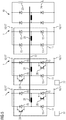
- the DC voltage network therefore has a precharge circuit 10.
- the following will be in connection with the FIG. 4 and 5 two possible embodiments of the precharge circuit 10 explained.
- the precharge circuit 10 of FIG. 4 has diode groups 11, a switching device 12, a power transmission path 13 and a control device 14.
- the number of diode groups 11 may be determined as needed. In the FIG. 4 shown number of three diode groups 11 is purely exemplary.
- the sections 1 of the DC voltage network are each connected to at least one of the diode groups 11 of the precharge circuit 10. Via the respective diode group 11, the sections 1 of the DC voltage network are coupled to the energy transmission path 13.
- the energy transmission path 13 is the same for the diode groups 11 and thus also for the sections 1 the same.
- the diode groups 11 for coupling in each case a single section 1 to the energy transmission path 13 may in the embodiment according to FIG. 4
- the respective section 1 is in this case connected to a node 16 which is arranged between the two diodes 15 of the respective diode group 11.
- the reference numerals for the diodes 15 and the node 16 are shown in FIG FIG. 4 drawn only for one diode group 11.
- the switching elements 5 of the sections 1 as shown in the FIGS. 2 and 3 each have a tap 17, which is arranged between the respective electronic switching device 6 and the respective electromechanical switch 7 of the respective switching path.
- the sections 1 can be connected via the respective tap 17 to the node 16 of the respective diode group 11.
- the switching paths of the switching elements 5, viewed in each case from the electronic switch arrangement 6, in each case have an electromechanical switch 7 in both directions
- the switching paths preferably also each have two taps 17.
- One of the two taps 17 is in this case arranged between the electronic switch arrangement 6 and the one electromechanical switch 7 and between the electronic switch arrangement 6 and the other electromechanical switch 7.
- the two taps 17 are connected in this case with different diode groups 11 of the precharge circuit 10.
- the control device 14 transmits a control signal S to the switching device 12.
- the switching device 12 is controlled such that it switches the energy transmission path 13 conductive. This effect is automatically obtained for all coupled to the energy transmission path 13 sections 1 of the DC voltage network.
- the switching device 12 may be disposed in the power transmission path 13.
- the switching device 12 may in the embodiment according to FIG. 4 For example, be designed as a simple electronic switch, in particular as an IGBT or as a MOSFET.
- a current-limiting element 18 is arranged in the energy transmission path 13.
- the current limiting element 18 may be formed as a resistor.
- the energy transmission path 13 is formed as a resistive energy transmission path.
- the current-limiting element 18 is designed as a throttle.
- the energy transmission path 13 is formed as an inductive energy transmission path.
- the element 18 In the case of the - preferred - embodiment of the current-limiting element 18 as a throttle, the element 18 strictly speaking, not the current I as such, but only its rise. Due to the fact that in the energy transmission path 13 of FIG. 4 no appreciable current limiting occurs, the current I flowing across the energy transfer path 13 can thus assume large values.
- a monitoring device 19 is present, which optionally the switching device 12 temporarily locks.
- the monitoring device 19 does not cause a permanent blocking of the switching device 12, but only serves to protect the pre-charge circuit 10 against overload.
- the monitoring device 19 can bring about a current limitation in the energy transmission path 13 and / or a temperature limitation of the switching device 12.
- the monitoring device 19 may be designed, for example, in the manner of a current regulator.
- the free-wheeling diode 20 is further connected in parallel to the current-limiting element 18.
- the freewheeling diode 20 can, for example, only bridge the current-limiting element 18. According to FIG. 4 the freewheeling diode 20 is connected to the negative potential P2.
- a capacitor 21 is still present.
- the capacitor 21 is used for commutation. It can be dimensioned so small that a pre-charging of the capacitor 21 is not required.
- a capacitor 22 may be present.
- the capacitor 22 serves to decouple the intrinsic inductances of the input lines of the pre-charge circuit 10.
- the energy transmission path 13 may additionally be assigned a resistor 23 and a further switching device 24 assigned to the resistor 23. Due to the presence of the series connection of the resistor 23 and the other switching device 24, it is possible to use the pre-charge circuit 10 as needed alternatively for pre-charging the sections 1 and for discharging the sections 1, depending on whether the resistor 23 via the further switching device 24 with the negative potential P2 is connected or disconnected from it.
- the energy transmission path 13 can thus act as a consumer when the other switching device 24 is closed.
- the embodiment of the Vorladescrien 10 according to FIG. 4 is only possible if by means of the switching elements 5 of the corresponding sections 1 only a single-pole separation of the sections 1 from each other.
- the configuration of the precharge circuit 10 is according to FIG. 5 always feasible, so both when using the switching elements 5 of the corresponding sections 1 only a one-pole separation of the sections 1 from each other, as well as when by means of the switching elements 5 of the corresponding sections 1 a two-pole separation of the sections 1 from each other.
- the precharge circuit 10 of FIG. 4 also has the precharge circuit 10 of FIG. 5 Diode groups 11, a switching device 12, a power transmission path 13 and a control device 14.
- the sections 1 of the DC voltage network are each connected to at least one of the diode groups 11 of the precharge circuit 10. Via the respective diode group 11, the sections 1 of the DC voltage network are coupled to the energy transmission path 13.
- the energy transmission path 13 is the same for the diode groups 11 and thus also for the sections 1 the same.
- the diode groups 11 for coupling in each case a single section 1 to the energy transmission path 13 may in the embodiment according to FIG. 5
- the respective section 1 is connected in this case with two nodes 16, which are arranged at the outputs of the bridge rectifier.
- the sections 1 of the DC voltage network are each connected to at least one of the diode groups 11 of the precharge circuit 10.
- the switching elements 5 of the sections 1 as shown in FIG. 3 in their two switching paths each have a tap 17, which is between the respective electronic switch assembly 6 and the respective electromechanical Switch 7 of the respective switching path is arranged.
- the sections 1 can be connected via the respective tap 17 to the node 16 of the respective diode group 11.
- taps 17 may be present and each one of the two taps 17 with one of the two nodes 16 may be connected.
- both potentials P1, P2 of the corresponding sections 1 are coupled to the energy transmission path 13 via the diode groups 11.
- the energy transmission path 13 is in the case of the embodiment of FIG. 5 from the diode groups 11 potential decoupled or galvanically isolated.
- the energy transmission path 13 in the case of the embodiment of FIG. 5 be designed in the manner of a transformer core, wherein in the bridge arms of the bridge rectifier windings 25 are arranged.
- the energy transmission path 13 is designed as an inductive energy transmission path.
- the windings 25 act - depending on the direction of the energy flow - as a primary winding or as a secondary winding of the transformer.
- the windings 25 have the same number of turns. It is therefore via the windings 25 and the energy transmission path 13 Although a potential decoupling, but no voltage transformation.
- the switching device 12 has a plurality of partial switching devices.
- the sub-switching devices are each assigned to a diode group 11. They each include two electronic switches 26, which are each connected in parallel to a diode 15. The two electronic switches 26 are arranged crosswise with respect to the bridge rectifier.
- the electronic switches 26 may be formed, for example, as an IGBT or as a MOSFET.
- the control device 14 transmits a control signal S to the switching device 12, by means of which the switching device 12 is controlled such that it switches the energy transmission path 13 to be conductive.
- the control signal S can cause the sub-switching devices to connect the section 1 connected to the respective diode group 11 in the manner of an inverter to the energy transmission path 13.
- the partial switching devices are preferably controlled uniformly by the control device 14. From the point of view of the control device 14, therefore, preferably only a single control signal S is output.
- the switching device 12 turns the power transmission path 13 conductive, feeds - as well as in the embodiment of FIG. 4 - Only that portion 1 energy in the energy transmission path 13, which has the highest voltage U.
- the switching device 12 draws energy from the energy transmission path 13, which has the lowest voltage U. This effect is automatically obtained for all coupled to the energy transmission path 13 sections 1 of the DC voltage network. As before, it can be determined by appropriate control of the electromechanical switch 7 of the switching elements 5, which sections 1 can ever be preloaded.
- monitoring devices 27 are preferably assigned to the subcircuit devices.
- the monitoring devices 27 only act on the respective partial switching device and lock it temporarily if necessary.
- the monitoring devices 27 do not cause a permanent blocking of the respective sub-switching device, but only serves to protect the respective sub-switching device against overload.
- the mode of operation of the monitoring devices 27 is analogous to the mode of operation of the monitoring device 19.
- each diode group 11 is assigned in each case a partial switching device.
- each diode group 11 is assigned in each case a partial switching device.
- the coupled sections 1 can only be precharged.
- the sections 1 coupled to these diode groups 11 can not feed electrical energy into the energy transmission path 13. If such diode groups 11 - ie diode groups 11 without associated partial switching device - are present, it is possible to mark the corresponding diode groups 11 accordingly, so that incorrect connections are avoided.
- Analogous to the embodiment of FIG. 4 can also in the design of FIG. 5 the energy transmission path 13 in addition, a resistor 23 and the resistor 23 associated with another switching device 24 be assigned. Due to the presence of the series connection of the resistor 23 and the other switching device 24, it is the same as in FIG. 4 it is possible to use the precharge circuit 10 alternatively as needed to pre-charge the sections 1 and to discharge the sections 1, depending on whether the resistor 23 is activated via the further switching device 24 or remains deactivated.
- the energy transmission path 13 can thus act as a consumer when the other switching device 24 is closed. If, however, sections 1 are coupled to the energy transmission path 13 exclusively via diode groups 11, that is to say that no subcircuit devices are assigned to them, these sections 1 can not be discharged via the resistor 23.
- the present invention has many advantages. For example, by means of the precharge circuit according to the invention it is possible to charge several sections 1 of the DC voltage network at the same time. In this case, it is ensured by the monitoring devices 19, 27 that the design limits of the precharge circuit 10 are not exceeded.
- the system is modular. In particular, multiple precharge circuits 10 may be used. For example, it is possible to use multiple precharge circuits 10 to increase the effective current. It is also possible to pre-load different groups of sections 1 via their own precharge circuit 10. For example, one precharge circuit 10 could be connected to the sections 1b to 1h, another precharge circuit 10 could be connected to the sections 1a, 1d and 1i to 1m.
- the precharge circuits 10 may in this case possibly be designed differently, that is, for example, once each according to FIG. 4 and FIG. 5 , In the case of the embodiment of the Vorladescrien 10 according to FIG. 5 Furthermore, it is possible to couple a separate energy source specifically for pre-charging the sections 1 to the energy transmission path 13.
- the winding 25 for coupling the power source can be adapted in this case with respect to their number of turns to the rated voltage of the power source in relation to the rated voltage of the DC power grid.
- the configuration of the precharge circuit 10 is very simple. The dimensioning of the precharge circuit 10 can be done as needed. Regardless of the dimensioning, however, even batteries included in sections 1 or other larger energy storage devices can be pre-charged.
- the diode groups 11 and, corresponding thereto, the inputs of the precharge circuit 10 do not have to be designed for the full power of the precharge circuit 10. If the corresponding necessity arises, it is possible, for example, to connect a specific section 1 of the DC voltage network-for example, section 1c-to two or three diode groups 11.
- a numerical example Assume that the switching device 12 and the energy transmission path 13 are dimensioned for an energy transfer of 1.5 kW, the diode groups 11 but dimensioned only for each 500 W.
- a specific section 1 of the DC voltage network is connected to three diode groups 11, it is possible to realize the full power transmission of 1.5 kW between this section 1 of the DC voltage network and the precharge circuit 10. It is even possible to dimension the diode groups 11 differently, for example a diode group 11 for a power transmission of 1.0 kW and another diode group 11 for a Energy transfer of 500 W.
- the sections 1 are always charged to the voltage U of the section 1 with the highest voltage U.
- the voltages of the sections 1 within the pre-charge circuit 10 can be measured and utilized for display, diagnostic or control purposes or transmitted to a higher-level device (for example a network management). It is also possible to give a message when the summons of the sections 1 is completed. It is also possible to end the pre-charging automatically when the duty cycle of the switching device 12 exceeds a predetermined value. In the case of the embodiment according to FIG. 4 Furthermore, it is possible to terminate the pre-charging automatically when the voltage difference across the diode groups 11 drops Threshold falls below or at the foot of the diode groups 11 adjusting potential has a sufficient distance from the negative potential P2. Starting the precharge can satisfy inverse conditions. In order to avoid a constant switching back and forth, the respective switching state of the precharge circuit 10 may be maintained for a minimum time or a hysteresis behavior may be implemented, if necessary.
Priority Applications (5)
| Application Number | Priority Date | Filing Date | Title |
|---|---|---|---|
| EP17162603.9A EP3379672A1 (fr) | 2017-03-23 | 2017-03-23 | Attribution efficace de sections d'un réseau de tension continu |
| US16/495,959 US10727668B2 (en) | 2017-03-23 | 2018-03-20 | Efficient pre-charging of sections of a DC voltage network |
| EP18716524.6A EP3583672B1 (fr) | 2017-03-23 | 2018-03-20 | Précharge efficace de sections d'un réseau de tension continu |
| PCT/EP2018/056941 WO2018172313A1 (fr) | 2017-03-23 | 2018-03-20 | Précharge efficace de sections d'un réseau à tension continue |
| CN201880020479.1A CN110462960B (zh) | 2017-03-23 | 2018-03-20 | 直流电压网的分段的有效预充电 |
Applications Claiming Priority (1)
| Application Number | Priority Date | Filing Date | Title |
|---|---|---|---|
| EP17162603.9A EP3379672A1 (fr) | 2017-03-23 | 2017-03-23 | Attribution efficace de sections d'un réseau de tension continu |
Publications (1)
| Publication Number | Publication Date |
|---|---|
| EP3379672A1 true EP3379672A1 (fr) | 2018-09-26 |
Family
ID=58448353
Family Applications (2)
| Application Number | Title | Priority Date | Filing Date |
|---|---|---|---|
| EP17162603.9A Withdrawn EP3379672A1 (fr) | 2017-03-23 | 2017-03-23 | Attribution efficace de sections d'un réseau de tension continu |
| EP18716524.6A Active EP3583672B1 (fr) | 2017-03-23 | 2018-03-20 | Précharge efficace de sections d'un réseau de tension continu |
Family Applications After (1)
| Application Number | Title | Priority Date | Filing Date |
|---|---|---|---|
| EP18716524.6A Active EP3583672B1 (fr) | 2017-03-23 | 2018-03-20 | Précharge efficace de sections d'un réseau de tension continu |
Country Status (4)
| Country | Link |
|---|---|
| US (1) | US10727668B2 (fr) |
| EP (2) | EP3379672A1 (fr) |
| CN (1) | CN110462960B (fr) |
| WO (1) | WO2018172313A1 (fr) |
Cited By (1)
| Publication number | Priority date | Publication date | Assignee | Title |
|---|---|---|---|---|
| CN112238763A (zh) * | 2020-10-23 | 2021-01-19 | 中车株洲电力机车有限公司 | 一种预充电/充电电路及其控制装置、控制方法 |
Citations (2)
| Publication number | Priority date | Publication date | Assignee | Title |
|---|---|---|---|---|
| US20130119903A1 (en) * | 2011-11-14 | 2013-05-16 | Rockwell Automation Technologies, Inc. | Ac pre-charge circuit |
| EP2595293A2 (fr) * | 2011-11-14 | 2013-05-22 | General Electric Company | Système de serrage et de préchargement pour système d'alimentation électrique et son procédé de fonctionnement |
Family Cites Families (6)
| Publication number | Priority date | Publication date | Assignee | Title |
|---|---|---|---|---|
| US6654262B2 (en) * | 2000-11-30 | 2003-11-25 | Mitsubishi Denki Kabushiki Kaisha | Inverter with pre-charging capacitor to reduce inrush current |
| EP1995818A1 (fr) * | 2007-05-12 | 2008-11-26 | Huettinger Electronic Sp. z o. o | Circuit et procédé de réduction d'énergie électrique stockée dans une inductance de cables d'alimentation pour une extinction rapide d'arcs à plasma |
| EP2810289B1 (fr) * | 2012-03-09 | 2016-05-04 | Siemens Aktiengesellschaft | Procédé de commutation d'un tronçon de réseaux de tension continue au moyen d'un interrupteur de tension continue |
| EP2871760B1 (fr) * | 2013-11-08 | 2018-03-21 | DET International Holding Limited | Précharge dépourvue de résistance |
| US20150229203A1 (en) * | 2014-02-12 | 2015-08-13 | Gholamreza Esmaili | Smart Resistor-Less Pre-Charge Circuit For Power Converter |
| US9787210B2 (en) * | 2015-01-14 | 2017-10-10 | Rockwell Automation Technologies, Inc. | Precharging apparatus and power converter |
-
2017
- 2017-03-23 EP EP17162603.9A patent/EP3379672A1/fr not_active Withdrawn
-
2018
- 2018-03-20 EP EP18716524.6A patent/EP3583672B1/fr active Active
- 2018-03-20 CN CN201880020479.1A patent/CN110462960B/zh active Active
- 2018-03-20 US US16/495,959 patent/US10727668B2/en active Active
- 2018-03-20 WO PCT/EP2018/056941 patent/WO2018172313A1/fr unknown
Patent Citations (2)
| Publication number | Priority date | Publication date | Assignee | Title |
|---|---|---|---|---|
| US20130119903A1 (en) * | 2011-11-14 | 2013-05-16 | Rockwell Automation Technologies, Inc. | Ac pre-charge circuit |
| EP2595293A2 (fr) * | 2011-11-14 | 2013-05-22 | General Electric Company | Système de serrage et de préchargement pour système d'alimentation électrique et son procédé de fonctionnement |
Cited By (2)
| Publication number | Priority date | Publication date | Assignee | Title |
|---|---|---|---|---|
| CN112238763A (zh) * | 2020-10-23 | 2021-01-19 | 中车株洲电力机车有限公司 | 一种预充电/充电电路及其控制装置、控制方法 |
| CN112238763B (zh) * | 2020-10-23 | 2022-05-13 | 中车株洲电力机车有限公司 | 一种充电电路及其控制装置、控制方法 |
Also Published As
| Publication number | Publication date |
|---|---|
| EP3583672A1 (fr) | 2019-12-25 |
| CN110462960A (zh) | 2019-11-15 |
| US10727668B2 (en) | 2020-07-28 |
| CN110462960B (zh) | 2023-07-28 |
| US20200136384A1 (en) | 2020-04-30 |
| EP3583672B1 (fr) | 2021-01-06 |
| WO2018172313A1 (fr) | 2018-09-27 |
Similar Documents
| Publication | Publication Date | Title |
|---|---|---|
| EP2425513B1 (fr) | Module avec un dispositif de stockage d'énergie électrique supplémentaire pour un convertisseur multi-niveaux modulaire | |
| EP3025403B1 (fr) | Convertisseur multipoints modulaire pour tensions élevées | |
| EP2493062B1 (fr) | Cellule de convertisseur CC-CC, circuit convertisseur ayant une capacité de retour monté à partir de celle-ci et son procédé de fonctionnement | |
| WO2017016674A1 (fr) | Module individuel, système électrique convertisseur de fréquence et système de batteries | |
| EP2458725A1 (fr) | Système convertisseur d'énergie électrique et procédé de son fonctionnement | |
| DE102010041040A1 (de) | Energieversorgungsnetz und Verfahren zum Laden mindestens einer als Energiespeicher für einen Gleichspannungszwischenkreis dienenden Energiespeicherzelle in einem Energieversorgungsnetz | |
| EP3211784A1 (fr) | Sous-module double pour un convertisseur de frequence multipoints modulaire et convertisseur de frequence multipoints modulaire en etant dote | |
| EP3230115B1 (fr) | Dispositif permettant de charger une unité batterie et de faire fonctionner une unité de charge par l'intermédiaire d'un onduleur | |
| EP2859569A1 (fr) | Commutateur de tension continue servant à commuter un courant continu dans une bifurcation d'un noeud de réseau de tension continue | |
| EP2532042B1 (fr) | Batterie à équilibrage inductif des cellules | |
| DE102013105098B4 (de) | Integrierter Solar-/Batteriewechselrichter | |
| EP3583672B1 (fr) | Précharge efficace de sections d'un réseau de tension continu | |
| EP3257145B1 (fr) | Convertisseur cc/cc avec condensateur flottant | |
| EP2745390B1 (fr) | Définition du potentiel de lignes d'entrée d'un onduleur | |
| WO2015090544A2 (fr) | Dispositif de stockage d'énergie électrique comprenant un circuit d'équilibrage | |
| EP2733837A1 (fr) | Convertisseur | |
| DE102013109714A1 (de) | Verfahren zum Betreiben einer elektrischen Schaltung sowie elektrische Schaltung | |
| DE102014201711A1 (de) | Energiespeichereinrichtung, System mit Energiespeichereinrichtung und Verfahren zum Ansteuern einer Energiespeichereinrichtung | |
| DE102015208568B4 (de) | Bordnetz-Schaltmodul, Bordnetzunterstützungseinrichtung und Bordnetzzweig | |
| EP3613124B1 (fr) | Alimentation sans interruption | |
| DE102019135128A1 (de) | Steckkontaktvorrichtung zur Vermeidung eines Lichtbogens beim Trennen einer Gleichstromverbindung | |
| DE102013207894A1 (de) | Elektrische Schaltung | |
| DE102014212263A1 (de) | Schaltungsanordnung zur selbstregelnden Anlaufstrombegrenzung einer elektrischen Maschine | |
| DE102014100257A1 (de) | Modularer Umrichter und Energieübertragungseinrichtung | |
| DE102013101652A1 (de) | Laststufenschalter mit Halbleiter-Schaltelementen und Verfahren zum Betrieb eines Laststufenschalters |
Legal Events
| Date | Code | Title | Description |
|---|---|---|---|
| PUAI | Public reference made under article 153(3) epc to a published international application that has entered the european phase |
Free format text: ORIGINAL CODE: 0009012 |
|
| AK | Designated contracting states |
Kind code of ref document: A1 Designated state(s): AL AT BE BG CH CY CZ DE DK EE ES FI FR GB GR HR HU IE IS IT LI LT LU LV MC MK MT NL NO PL PT RO RS SE SI SK SM TR |
|
| AX | Request for extension of the european patent |
Extension state: BA ME |
|
| STAA | Information on the status of an ep patent application or granted ep patent |
Free format text: STATUS: THE APPLICATION IS DEEMED TO BE WITHDRAWN |
|
| 18D | Application deemed to be withdrawn |
Effective date: 20190327 |