EP3379538A1 - Embedded memory with setup-hold time controlled internally or externally and associated integrated circuit - Google Patents
Embedded memory with setup-hold time controlled internally or externally and associated integrated circuit Download PDFInfo
- Publication number
- EP3379538A1 EP3379538A1 EP17208158.0A EP17208158A EP3379538A1 EP 3379538 A1 EP3379538 A1 EP 3379538A1 EP 17208158 A EP17208158 A EP 17208158A EP 3379538 A1 EP3379538 A1 EP 3379538A1
- Authority
- EP
- European Patent Office
- Prior art keywords
- clock signal
- circuit
- delay
- clock
- path
- Prior art date
- Legal status (The legal status is an assumption and is not a legal conclusion. Google has not performed a legal analysis and makes no representation as to the accuracy of the status listed.)
- Granted
Links
Images





Classifications
-
- G—PHYSICS
- G11—INFORMATION STORAGE
- G11C—STATIC STORES
- G11C7/00—Arrangements for writing information into, or reading information out from, a digital store
- G11C7/22—Read-write [R-W] timing or clocking circuits; Read-write [R-W] control signal generators or management
-
- G—PHYSICS
- G11—INFORMATION STORAGE
- G11C—STATIC STORES
- G11C7/00—Arrangements for writing information into, or reading information out from, a digital store
- G11C7/22—Read-write [R-W] timing or clocking circuits; Read-write [R-W] control signal generators or management
- G11C7/222—Clock generating, synchronizing or distributing circuits within memory device
-
- G—PHYSICS
- G06—COMPUTING OR CALCULATING; COUNTING
- G06F—ELECTRIC DIGITAL DATA PROCESSING
- G06F30/00—Computer-aided design [CAD]
- G06F30/30—Circuit design
-
- G—PHYSICS
- G11—INFORMATION STORAGE
- G11C—STATIC STORES
- G11C7/00—Arrangements for writing information into, or reading information out from, a digital store
- G11C7/10—Input/output [I/O] data interface arrangements, e.g. I/O data control circuits, I/O data buffers
- G11C7/1006—Data managing, e.g. manipulating data before writing or reading out, data bus switches or control circuits therefor
-
- G—PHYSICS
- G11—INFORMATION STORAGE
- G11C—STATIC STORES
- G11C7/00—Arrangements for writing information into, or reading information out from, a digital store
- G11C7/10—Input/output [I/O] data interface arrangements, e.g. I/O data control circuits, I/O data buffers
- G11C7/1078—Data input circuits, e.g. write amplifiers, data input buffers, data input registers, data input level conversion circuits
-
- G—PHYSICS
- G11—INFORMATION STORAGE
- G11C—STATIC STORES
- G11C7/00—Arrangements for writing information into, or reading information out from, a digital store
- G11C7/10—Input/output [I/O] data interface arrangements, e.g. I/O data control circuits, I/O data buffers
- G11C7/1078—Data input circuits, e.g. write amplifiers, data input buffers, data input registers, data input level conversion circuits
- G11C7/109—Control signal input circuits
-
- G—PHYSICS
- G11—INFORMATION STORAGE
- G11C—STATIC STORES
- G11C7/00—Arrangements for writing information into, or reading information out from, a digital store
- G11C7/10—Input/output [I/O] data interface arrangements, e.g. I/O data control circuits, I/O data buffers
- G11C7/1078—Data input circuits, e.g. write amplifiers, data input buffers, data input registers, data input level conversion circuits
- G11C7/1093—Input synchronization
-
- G—PHYSICS
- G11—INFORMATION STORAGE
- G11C—STATIC STORES
- G11C7/00—Arrangements for writing information into, or reading information out from, a digital store
- G11C7/12—Bit line control circuits, e.g. drivers, boosters, pull-up circuits, pull-down circuits, precharging circuits, equalising circuits, for bit lines
-
- G—PHYSICS
- G11—INFORMATION STORAGE
- G11C—STATIC STORES
- G11C8/00—Arrangements for selecting an address in a digital store
- G11C8/06—Address interface arrangements, e.g. address buffers
-
- G—PHYSICS
- G11—INFORMATION STORAGE
- G11C—STATIC STORES
- G11C8/00—Arrangements for selecting an address in a digital store
- G11C8/18—Address timing or clocking circuits; Address control signal generation or management, e.g. for row address strobe [RAS] or column address strobe [CAS] signals
-
- G—PHYSICS
- G06—COMPUTING OR CALCULATING; COUNTING
- G06F—ELECTRIC DIGITAL DATA PROCESSING
- G06F13/00—Interconnection of, or transfer of information or other signals between, memories, input/output devices or central processing units
- G06F13/14—Handling requests for interconnection or transfer
- G06F13/16—Handling requests for interconnection or transfer for access to memory bus
- G06F13/1668—Details of memory controller
- G06F13/1689—Synchronisation and timing concerns
Definitions
- the present invention relates to an integrated circuit design, and more particularly, to an embedded memory with a setup-hold time that can be controlled internally or externally and an associated integrated circuit.
- SoC system-on-chip
- the traditional timing sign-off may reserve a 3-sigma local variation factor for hold-time margin.
- DPPM defective parts per million
- the DPPM can be improved.
- the DPPM is improved at the expense of chip area, timing closure and speed performance. As a result, the SoC design suffers from chip area, timing closure and speed performance, inevitably.
- the memory built-in self-test (MBIST) logic of the embedded memory is unable to identify hold-time violations at the memory input interface and the MBIST logic itself. This may result in holes in the MBIST Shmoo plot.
- One of the objectives of the claimed invention is to provide an embedded memory with a setup-hold time that can be controlled internally/externally and an associated integrated circuit.
- an exemplary embedded memory in an integrated circuit includes a memory interface circuit, a cell array, and a peripheral circuit.
- the memory interface circuit includes a plurality of interface pins and a programmable path delay circuit.
- the interface pins are arranged to receive at least a clock signal, a non-clock signal, and a setup-hold time control setting.
- the programmable path delay circuit is arranged to set a path delay of at least one of a clock path and a non-clock path according to the setup-hold time control setting, wherein the clock path is arranged to deliver the clock signal, and the non-clock path is arranged to deliver the non-clock signal.
- the cell array has a plurality of memory cells.
- the peripheral circuit is arranged to access the cell array according to at least the clock signal provided from the clock path and the non-clock signal provided from the non-clock path.
- an exemplary integrated circuit includes a clock tree, a flip-flop circuit, an embedded memory, and a clock-gating cell circuit.
- the clock tree is arranged to distribute at least a first clock signal and a second clock signal.
- the flip-flop circuit has a clock input port and a data output port, wherein the clock input port is arranged to receive the first clock signal from the clock tree via the clock-gating cell circuit, and the data output port is arranged to output a non-clock signal.
- the embedded memory is arranged to receive the second clock signal from the clock tree, receive the non-clock signal from the flip-flop circuit, and perform memory access according to at least the second clock signal and the non-clock signal.
- the clock-gating cell circuit is arranged to receive the first clock signal, and selectively provide the first clock signal to the clock input port of the flip-flop circuit.
- the clock-gating cell circuit comprises a programmable path delay circuit arranged to set a path delay of a clock path according to a setup-hold time control setting, wherein the clock path is arranged to deliver the first clock signal.
- Embodiments of the present invention proposes an embedded memory with a setup-hold time that can be controlled internally or externally, thereby avoiding hold-time violations at the memory input interface. In this way, the "Shmoo hole" issue can be relaxed by the proposed solution. In addition, the SoC timing closure can also benefit from the proposed solution.
- FIG. 1 is a diagram illustrating a first integrated circuit design according to an embodiment of the present invention.
- the integrated circuit is a system-on-chip (SoC) 10 having embedded memories included therein.
- SoC system-on-chip
- the embedded memory 100 includes a cell array 102, a peripheral circuit 104, and a memory interface circuit 106.
- the cell array 102 has a plurality of memory cells 108. Each memory cell 108 can be assessed by enabling one word line and one bit line at which the memory cell 108 is located.
- the peripheral circuit 104 includes circuit elements needed to access (read/write) the cell array 102.
- the peripheral circuit 104 may include a row decoder, row drivers, a clock generator, a timing controller, a column decoder, sense amplifiers, data latches, etc.
- the memory interface circuit 106 includes a plurality of interface pins 110 and a programmable path delay circuit 112. The interface pins 110 are arranged to receive a clock signal, a plurality of non-clock signals, and a delay selection signal.
- the interface pins 110 include one clock pin defined to receive a clock signal CK (which is an external clock generated from a clock source), one chip select (CS) pin defined to receive a CS signal (which is a non-clock signal), one write enable (WE) pin defined to receive a WE signal (which is a non-clock signal), one bit write enable (BYTE) pin defined to receive a BYTE signal (which is a non-clock signal), a plurality of address (ADR) pins defined to receive ADR bits (which are non-clock signals), a plurality of data input (DI) pins defined to receive DI bits (which are non-clock signals), and a plurality of delay select (DELSEL) pins defined to receive a delay selection signal composed of one or more DELSEL bits.
- CK which is an external clock generated from a clock source
- CS chip select
- WE write enable
- BYTE bit write enable
- ADR address
- DI data input
- DI data input
- DELSEL delay select
- a setup-hold time control setting SHSEL may be inputted by at least a portion (i.e., part or all) of the DELSEL bits, depending upon the actual design considerations.
- the peripheral circuit 104 reads/writes the cell array 102 according to at least the clock signal CK provided from a clock path and non-clock signal (s) provided from non-clock path(s). Since an embodiment of the present invention focuses on the memory interface design (particularly, the programmable path delay circuit 112), further description of cell array 102 and peripheral circuit 104 is omitted here for brevity.
- FIG. 1 Only the circuit elements pertinent to the present invention are shown in FIG. 1 .
- the embedded memory 100 may have additional circuit elements to achieve other designated functions.
- the embedded memory 100 has a programmable input path delay controlled by the programmable path delay circuit 112. Hence, a programmable setup time and a programmable hold time of each non-clock signal received from an interface pin (e.g., a control pin, an address pin, or a data input pin) can be achieved at the memory interface circuit 106.
- an interface pin e.g., a control pin, an address pin, or a data input pin
- the programmable path delay circuit 112 is arranged to set a path delay of a clock path according to the setup-hold time control setting SHSEL, where the clock path is used to deliver the clock signal CK received by one interface pin 110.
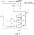
- FIG. 2 is a diagram illustrating a first exemplary design of the programmable path delay circuit 112 shown in FIG. 1 according to an embodiment of the present invention.
- the programmable path delay circuit 112 includes a plurality of delay cell circuits 206, 208 and a plurality of multiplexers (MUXs) 210, 212, 214.
- MUXs multiplexers
- FIG. 2 and the number of multiplexers shown in FIG. 2 are for illustrative purposes only, and are not meant to be limitations of the present invention. In practice, the number of delay cell circuits and the number of multiplexers may be adjusted, depending upon actual design considerations.
- the programmable path delay circuit 112 receives the clock signal CK from one interface pin 110, and delivers the clock signal CK to each latch 202 in the peripheral circuit 104 via the clock path 204, where each of the latches 202 (e.g., latch[0]-latch[n]) receives one non-clock signal Non_CK received from one interface pin 110 and an internal clock signal Int_CK provided from the programmable path delay circuit 112.
- the non-clock signal Non_CK may be a CS signal, a WE signal, a BYTE signal, an ADR bit, a DI bit, or any synchronous input of the embedded memory 100.
- Each of the delay cell circuits 206 and 208 is arranged to apply a predetermined delay amount to the clock signal CK. It should be noted that the delay cell circuits 206 and 208 may be implemented using the same delay cell design to offer the same predetermined delay amount, or may be implemented using different delay cell designs to offer different predetermined delay amounts. Consider a case where the delay cell circuits 206 and 208 may be implemented using the same delay cell design to offer the same predetermined delay amount DL. If the clock signal CK passes through one delay cell circuit, the clock signal CK is delayed by DL*1. If the clock signal CK passes through two delay cell circuits, the clock signal CK is delayed by DL*2.
- the multiplexer 210 has an input port and an output port, wherein the input port is arranged to receive the clock signal CK without via any of the delay cell circuits 206 and 208, and the output port is arranged to selectively output the clock signal CK received at the input port according to the setup-hold time control setting SHSEL.
- the multiplexer 212 has an input port and an output port, wherein the input port is arranged to receive the clock signal CK via the delay cell circuit 206, and the output port is arranged to selectively output the clock signal CK received at the input port according to the setup-hold time control setting SHSEL.
- the multiplexer 214 has an input port and an output port, wherein the input port is arranged to receive the clock signal CK via the delay cell circuits 206 and 208, and the output port is arranged to selectively output the clock signal CK received at the input port according to the setup-hold time control setting SHSEL.
- the setup-hold time control setting SHSEL determines which one of the multiplexers 210, 212, 214 is enabled to output the received clock signal to the following latch 202.
- a clock signal CK1 (which is generated by passing the clock signal CK through the multiplexer 210) is used to act as the internal clock signal Int_CK.
- a clock signal CK2 (which is generated by passing the clock signal CK through the delay cell circuit 206 and the multiplexer 212) is used to act as the internal clock signal Int_CK.
- a clock signal CK3 (which is generated by passing the clock signal CK through the delay cell circuits 206, 208 and the multiplexer 214) is used to act as the internal clock signal Int_CK.
- each of the clock signals CK1, CK2, CK3 may be regarded as the clock signal CK with a programmable clock skew.
- the path delay of the clock path 204 can be adjusted, thereby affecting the setup time and the hold time of the non-clock signal Non_CK with respect to the internal clock signal Int_CK (which may be regarded as a clock signal CK with a programmable memory interface delay).
- FIG. 3 is a diagram illustrating waveforms of clock signals CK, CK1, CK2, CK3 and non-clock signal Non_CK according to an embodiment of the present invention.
- the clock signals CK, CK1, CK2, CK3 have the same frequency but different phases.
- a phase delay between the clock signals CK1 and CK results from the multiplexer 210.
- a phase delay between the clock signals CK2 and CK results from the delay cell circuit 206 and the multiplexer 212.
- a phase delay between the clock signals CK3 and CK results from the delay cell circuits 206, 208 and the multiplexer 214.
- a setup time T setup is the amount of time the input signal should be held steady before a clock edge occurs.
- the hold time T hold is the amount of time the input signal should be held steady after the clock edge occurs.
- the timing of the clock edge of the internal clock signal Int_CK can be adjusted to avoid the setup time violation and/or the hold time violation of the non-clock signal Non_CK at the latch 202.
- the hold time passes the timing requirement when the internal clock signal Int_CK is set by the clock signal CK1; the hold time marginally passes the timing requirement when the internal clock signal Int_CK is set by the clock signal CK2; and the hold time fails to pass the timing requirement when the internal clock signal Int_CK is set by the clock signal CK2.
- the setup-hold time control setting SHSEL may be set to enable the multiplexer 210, thereby outputting the clock signal CK1 to the latch 202.
- the waveforms shown in FIG. 3 are for illustrative purposes only, and are not meant to be limitations of the present invention.
- one of the clock signals CK1, CK2, CK3 may be selected on the basis of the actual timing relation between the clock signal CK and the non-clock signal Non_CK.
- FIG. 4 is a diagram illustrating a circuit design of the programmable path delay circuit 112 shown in FIG. 2 according to an embodiment of the present invention.
- the delay cell circuit 208 is implemented using two inverters INV2 and INV3.
- the multiplexer 210 is implemented using P-channel metal-oxide-semiconductor field effect transistors (PMOS transistors) MP1, MP2 and N-channel metal-oxide-semiconductor field effect transistors (NMOS transistors) MN1, MN2.
- the multiplexer 212 is implemented using PMOS transistors MP3, MP4 and NMOS transistors MN3, MN4.
- the setup-hold time control setting SHSEL includes one control bit DELSEL.
- the inverter INV1 sets another control bit DELSELB by inverting a logic level of the control bit DELSEL. In other words, when the control bit DELSEL has a high logic value "1", the control bit DELSELB has a low logic value "0"; and when the control bit DELSEL has a low logic value "0", the control bit DELSELB has a high logic value "1".
- the control bit DELSEL is set by the low logic value "0"
- the multiplexer 210 is enabled, while the multiplexer 212 is disabled.
- the clock signal CK passes through the multiplexer 210, and is further processed by an inverter INV4 to become the internal clock Int_CK.
- the control bit DELSEL is set by the high logic value "1”
- the multiplexer 210 is disabled, while the multiplexer 212 is enabled.
- the clock signal CK passes through the delay cell circuit 208 and the multiplexer 212, and is further processed by the inverter INV4 to become the internal clock signal Int_CK.
- the circuit implementation shown in FIG. 4 is for illustrative purposes only, and is not meant to be a limitation of the present invention. That is, the same objective of programming the path delay of the clock path 204 may be achieved by implementing the programmable path delay circuit 112 shown in FIG. 2 with another circuit design.
- the path delay of the clock path 204 is programmed by an integer number of gate delays.
- the granularity of programming the path delay of the clock path 204 depends on the gate delay.
- the present invention proposes another design of the programmable path delay circuit 112 shown in FIG. 1 .
- FIG. 5 is a diagram illustrating a second exemplary design of the programmable path delay circuit 112 shown in FIG. 1 according to an embodiment of the present invention.
- the programmable path delay circuit 112 includes a base delay circuit 502, a first delay control circuit 504, and a second delay control circuit 506.
- the programmable path delay circuit 112 receives the clock signal CK from one interface pin 110, and delivers the clock signal CK to each latch 202 in the peripheral circuit 104 via a clock path 501, where each of the latches 202 receives one non-clock signal Non_CK received from one interface pin 110 and an internal clock signal Int_CK provided from the programmable path delay circuit 112.
- the non-clock signal Non_CK may be a CS signal, a WE signal, a BYTE signal, an ADR bit, a DI bit, or any synchronous input of the embedded memory 100.
- the base delay circuit 502 is arranged to receive the clock signal CK, and apply a programmable delay amount to the clock signal CK. In other words, when the clock signal CK passes through the base delay circuit 502, the clock signal CK is delayed by the programmable delay amount.
- the first delay control circuit 504 includes a plurality of first transistors M 11 -M 1N connected in parallel between a first node N1 of the base delay circuit 502 and a supply voltage VDD.
- the second delay control circuit 506 includes a plurality of second transistors M 21 -M 2N connected in parallel between a second node N2 of the base delay circuit 502 and a ground voltage GND.
- the number of first transistors M 11 -M 1N implemented in the first delay control circuit 504 and the number of second transistors M 21 -M 2N implemented in the second delay control circuit 506 may be adjusted, depending upon the actual design considerations.
- the number of turned-on first transistors in the first delay control circuit 504 and the number of turned-on second transistors in the second delay control circuit 506 are both controlled by the setup-hold time control setting SHSEL.
- the programmable delay amount of the base delay circuit 502 is determined by the number of turned-on first transistors in the first delay control circuit 504 and the number of turned-on second transistors in the second delay control circuit 506. For example, the programmable delay amount of the base delay circuit 502 is set by a first delay time when the number of turned-on first transistors in the first delay control circuit 504 is set by a first value and the number of turned-on second transistors in the second delay control circuit 506 is set by the same first value; and the programmable delay amount of the base delay circuit 502 is set by a second delay time when the number of turned-on first transistors in the first delay control circuit 504 is set by a second value and the number of turned-on second transistors in the second delay control circuit 506 is set by the same second value.
- the first delay time is shorter than the second delay time due to a larger driving current used by the base delay circuit 502; and if the first value is smaller than the second value, the first delay time is longer than the second delay time due to a smaller driving current used by the base delay circuit 502.
- the timing of the clock edge of the internal clock signal Int_CK can be adjusted to avoid the setup time violation and/or the hold time violation of the non-clock signal Non_CK at the latch 202.
- the programmable path delay circuit 112 shown in FIG. 5 controls the path delay of the clock path 501 through tuning the magnitude of the driving current used by the base delay circuit 502. Compared to the programmable path delay circuit 112 shown in FIG. 2 , the programmable path delay circuit 112 shown in FIG. 5 is capable of controlling the path delay with finer granularity.
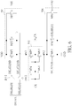
- FIG. 6 is a diagram illustrating a circuit design of the programmable path delay circuit 112 shown in FIG. 5 according to an embodiment of the present invention.
- the first delay control circuit 504 is implemented using PMOS transistors MP1, MP2, MP3.
- the second delay control circuit 506 is implemented using NMOS transistors MN1, MN2, MN3.
- each of the first delay control circuit 504 and the second delay control circuit 506 is shown having three transistors only.
- the base delay circuit 502 is implemented using PMOS transistors MP4, MP5 and NMOS transistors MN4, MN5, where PMOS transistor MP4 and NMOS transistor MN4 form one inverter, and PMOS transistor MP5 and NMOS transistor MN5 form another inverter.
- the setup-hold time control setting SHSEL includes one control input DELSEL composed of two control bits DELSEL[0] and DELSEL[1].
- the inverter INV1 sets another control bit DELSEL[0]B by inverting a logic level of the control bit DELSEL[0].
- the inverter INV2 sets yet another control bit DELSEL[1]B by inverting a logic level of the control bit DELSEL[1]. In other words, when the control bit DELSEL[0] has a high logic value "1", the control bit DELSEL[0]B has a low logic value "0"; and when the control bit DELSEL[0] has a low logic value "0”, the control bit DELSEL[0]B has a high logic value "1".
- the control bit DELSEL[1] has a high logic value "1”
- the control bit DELSEL[1]B has a low logic value "0”
- the control bit DELSEL[1]B has a high logic value "1”.
- the PMOS transistor MP3 is turned on by a first bias voltage VB1 (e.g., ground voltage GND)
- the NMOS transistor NP3 is turned on by a second bias voltage VB2 (e.g., supply voltage VDD).
- VB1 ground voltage GND
- the NMOS transistor NP3 is turned on by a second bias voltage VB2 (e.g., supply voltage VDD).
- the PMOS transistor MP3 is turned on regardless of on/off statuses of PMOS transistors MP1 and MP2
- the NMOS transistor MN3 is turned on regardless of on/off statuses of NMOS transistors MN1 and MN2.
- the first delay control circuit 504 has only one turned-on PMOS transistor MP3, and the second delay control circuit 506 has only one turned-on NMOS transistor MN3.
- the path delay of the clock path 204 is programmed to have a largest delay amount due to a smallest driving current.
- the first delay control circuit 504 has two turned-on PMOS transistors (e.g., MP1 and MP3, or MP2 and MP3), and the second delay control circuit 506 has two turned-on NMOS transistors (e.g., MN1 and MN3, or MN2 and MN3).
- the path delay of the clock path 204 is programmed to have a medium delay amount due to a medium driving current.
- the first delay control circuit 504 has three turned-on PMOS transistors MP1, MP2, MP3, and the second delay control circuit 506 has three turned-on NMOS transistors MN1, MN2, MN3.
- the path delay of the clock path 204 is programmed to have a smallest delay amount due to a largest driving current.
- circuit implementation shown in FIG. 6 is for illustrative purposes only, and is not meant to be a limitation of the present invention. That is, the same objective of programming the path delay of the clock path 501 may be achieved by implementing the programmable path delay circuit 112 shown in FIG. 5 with another circuit design.
- any of the setup time T setup and the hold time T hold violates the timing requirement depends on the relative timing relation between a clock signal and a non-clock signal (which is to be sampled by the clock signal). Adjusting the timing of the clock signal is able to affect the setup time T setup and the hold time T hold . Alternatively, adjusting the timing of the non-clock signal is also able to affect the setup time T setup and the hold time T hold .
- the programmable path delay circuit 112 is arranged to set a path delay of a non-clock path according to the setup-hold time control setting SHSEL, where the non-clock path is used to deliver a non-clock signal (e.g., a CS signal, a WE signal, a BYTE signal, an ADR bit, a DI bit, or any synchronous input) received by one interface pin 110 of the embedded memory 100.
- a non-clock signal e.g., a CS signal, a WE signal, a BYTE signal, an ADR bit, a DI bit, or any synchronous input
- FIG. 7 is a diagram illustrating a third exemplary design of the programmable path delay circuit 112 shown in FIG. 1 according to an embodiment of the present invention.
- the programmable path delay circuit 112 may include a plurality of circuit modules 702, each arranged to provide one non-clock signal Non_CK to one of a plurality of latches 202 in the peripheral circuit 104.
- Each circuit module 702 in the programmable path delay circuit 112 includes a plurality of delay cell circuits 706, 708 and a plurality of multiplexers (MUXs) 710, 712, 714.
- MUXs multiplexers
- Each circuit module 702 of the programmable path delay circuit 112 receives the non-clock signal Non_CK (e.g., a CS signal, a WE signal, a BYTE signal, an ADR bit, a DI bit, or any synchronous input of the embedded memory 100) from one interface pin 110, and delivers the non-clock signal Non_CK to one latch 202 via a non-clock path 704, where each latch 202 receives the clock signal CK received from one interface pin 110 and one non-clock signal Non_CK provided from the programmable path delay circuit 112.
- the non-clock signal Non_CK e.g., a CS signal, a WE signal, a BYTE signal, an ADR bit, a DI bit, or any synchronous input of the embedded memory 100
- Each of the delay cell circuits 706 and 708 is arranged to apply a predetermined delay amount to the non-clock signal Non_CK. It should be noted that the delay cell circuits 706 and 708 may be implemented using the same delay cell design to offer the same predetermined delay amount, or may be implemented using different delay cell designs to offer different predetermined delay amounts. Consider a case where the delay cell circuits 706 and 708 may be implemented using the same delay cell design to offer the same predetermined delay amount DL. If the non-clock signal Non_CK passes through one delay cell circuit, the non-clock signal Non_CK is delayed by DL*1. If the non-clock signal Non_CK passes through two delay cell circuits, the non-clock signal Non_CK is delayed by DL*2.
- the multiplexer 710 has an input port and an output port, wherein the input port is arranged to receive the non-clock signal Non_CK without via any of the delay cell circuits 706 and 708, and the output port is arranged to selectively output the non-clock signal Non_CK received at the input port according to the setup-hold time control setting SHSEL.
- the multiplexer 712 has an input port and an output port, wherein the input port is arranged to receive the non-clock signal Non_CK via the delay cell circuit 706, and the output port is arranged to selectively output the non-clock signal Non_CK received at the input port according to the setup-hold time control setting SHSEL.
- the multiplexer 714 has an input port and an output port, wherein the input port is arranged to receive the non-clock signal Non_CK via the delay cell circuits 706 and 708, and the output port is arranged to selectively output the non-clock signal Non_CK received at the input port according to the setup-hold time control setting SHSEL.
- the setup-hold time control setting SHSEL determines which one of the multiplexers 710, 712, 714 is enabled to output the received non-clock signal to the following latch 202.
- a non-clock signal Non_CK1 (which is generated by passing the non-clock signal Non_CK through the multiplexer 710) is used to act as the non-clock input of the latch 202.
- a non-clock signal Non_CK2 (which is generated by passing the non-clock signal Non_CK through the delay cell circuit 706 and the multiplexer 712) is used to act as the non-clock input of the latch 202.
- a non-clock signal Non_CK3 (which is generated by passing the non-clock signal Non_CK through the delay cell circuits 706, 708 and the multiplexer 714) is used to act as the non-clock input of the latch 202.
- the path delay of the non-clock path 704 can be adjusted, thereby affecting the setup time and the hold time of the non-clock input (which may be regarded as a non-clock signal Non_CK with a programmable memory interface delay) with respect to the clock signal CK.
- FIG. 8 is a diagram illustrating waveforms of non-clock signals Non_CK, Non_CK1, Non_CK2, Non_CK3 and clock signal CK according to an embodiment of the present invention.
- the non-clock signals Non_CK, Non_CK1, Non_CK2, Non_CK3 have the same waveform but different timing.
- a timing delay between the non-clock signals Non_CK1 and Non_CK results from the multiplexer 710.
- a timing delay between the non-clock signals Non_CK2 and Non_CK results from the delay cell circuit 706 and the multiplexer 712.
- a timing delay between the non-clock signals Non_CK3 and Non_CK results from the delay cell circuits 706, 708 and the multiplexer 714.
- the timing of the non-clock input can be adjusted to avoid the setup time violation and/or the hold time violation of the non-clock signal Non_CK at the latch 202.
- the setup time passes the timing requirement when the non-clock input is set by the non-clock signal Non_CK1; the setup time marginally passes the timing requirement when the non-clock input is set by the non-clock signal Non_CK2; and the setup time fails to pass the timing requirement when the non-clock input is set by the non-clock signal Non_CK3.
- the setup-hold time control setting SHSEL may be set to enable the multiplexer 710, thereby outputting the non-clock signal Non_CK1 to the latch 202.
- one of the non-clock signals Non_CK1, Non_CK2, Non_CK3 may be selected on the basis of the actual timing relation between the clock signal CK and the non-clock signal Non_CK.
- each circuit module 702 in the programmable path delay circuit 112 shown in FIG. 7 is similar to that of the programmable path delay circuit 112 shown in FIG. 2 .
- the major difference is that an input of each circuit module 702 in the programmable path delay circuit 112 shown in FIG. 7 is a non-clock signal Non_CK (e.g., a CS signal, a WE signal, a BYTE signal, an ADR bit, a DI bit, or any synchronous input).
- Non_CK e.g., a CS signal, a WE signal, a BYTE signal, an ADR bit, a DI bit, or any synchronous input.
- each circuit module 702 in the programmable path delay circuit 112 may also be implemented using the circuit design shown in FIG. 4 . Further description is omitted here for brevity.
- FIG. 9 is a diagram illustrating a fourth exemplary design of the programmable path delay circuit 112 shown in FIG. 1 according to an embodiment of the present invention.
- the programmable path delay circuit 112 may include a plurality of circuit modules 902, each arranged to receive a non-clock signal Non_CK from one interface pin 110 and deliver the non-clock signal Non_CK to one latch 202 in the peripheral circuit 104 via a non-clock path 901.
- Each circuit module 902 in the programmable path delay circuit 112 includes a base delay circuit 902, a first delay control circuit 904, and a second delay control circuit 906.
- Each latch 202 receives the clock signal CK from one interface pin 110 and one non-clock signal Non_CK provided from the programmable path delay circuit 112.
- the non-clock signal Non_CK may be a CS signal, a WE signal, a BYTE signal, an ADR bit, a DI bit, or any synchronous input of the embedded memory 100.
- the base delay circuit 902 is arranged to receive the non-clock signal Non_CK, and apply a programmable delay amount to the non-clock signal Non_CK. In other words, when the non-clock signal Non_CK passes through the base delay circuit 902, the non-clock signal Non_CK is delayed by the programmable delay amount.
- the first delay control circuit 904 includes a plurality of first transistors M 11 -M 1N connected in parallel between a first node N1 of the base delay circuit 902 and a supply voltage VDD.
- the second delay control circuit 906 includes a plurality of second transistors M 21 -M 2N connected in parallel between a second node N2 of the base delay circuit 902 and a ground voltage GND.
- the number of first transistors M 11 -M 1N implemented in the first delay control circuit 904 and the number of second transistors M 21 -M 2N implemented in the second delay control circuit 906 may be adjusted, depending upon the actual design considerations.
- the number of turned-on first transistors in the first delay control circuit 904 and the number of turned-on second transistors in the second delay control circuit 906 are both controlled by the setup-hold time control setting SHSEL.
- the programmable delay amount of the base delay circuit 902 is determined by the number of turned-on first transistors in the first delay control circuit 904 and the number of turned-on second transistors in the second delay control circuit 906. For example, the programmable delay amount of the base delay circuit 902 is set by a first delay time when the number of turned-on first transistors in the first delay control circuit 904 is set by a first value and the number of turned-on second transistors in the second delay control circuit 906 is set by the same first value; and the programmable delay amount of the base delay circuit 902 is set by a second delay time when the number of turned-on first transistors in the first delay control circuit 904 is set by a second value and the number of turned-on second transistors in the second delay control circuit 906 is set by the same second value.
- the first delay time is shorter than the second delay time due to a larger driving current used by the base delay circuit 902; and if the first value is smaller than the second value, the first delay time is longer than the second delay time due to a smaller driving current used by the base delay circuit 902.
- the timing of the non-clock input can be adjusted to avoid the setup time violation and/or the hold time violation of the non-clock input at the latch 202.
- the programmable path delay circuit 112 shown in FIG. 9 controls the path delay of the clock path 901 through tuning the magnitude of the driving current used by the base delay circuit 902. Compared to the programmable path delay circuit 112 shown in FIG. 7 , the programmable path delay circuit 112 shown in FIG. 9 is capable of controlling the path delay with finer granularity.
- each circuit module 902 in the programmable path delay circuit 112 shown in FIG. 9 is similar to that of the programmable path delay circuit 112 shown in FIG. 5 .
- the major difference is that an input of each circuit module 902 in the programmable path delay circuit 112 shown in FIG. 9 is a non-clock signal Non_CK (e.g., a CS signal, a WE signal, a BYTE signal, an ADR bit, a DI bit, or any synchronous input).
- Non_CK e.g., a CS signal, a WE signal, a BYTE signal, an ADR bit, a DI bit, or any synchronous input.
- each circuit module 902 in the programmable path delay circuit 112 may also be implemented using the circuit design shown in FIG. 6 . Further description is omitted here for brevity.
- the programmable path delay circuit 112 is used to set a path delay of only one of a clock path and a non-clock path according to the setup-hold time control setting.
- the programmable path delay circuit 112 may be modified to set path delays of both of a clock path and a non-clock path according to the setup-hold time control setting. This alternative design also falls within the scope of the present invention.
- Adjusting the timing of the non-clock signal is also able to affect the setup time T setup and the hold time T hold .
- the embedded memory 100 has the memory interface circuit 106 equipped with the programmable path delay circuit 112 for achieving the objective of adjusting the timing of the non-clock signal at the memory interface.
- the above embodiments propose an embedded memory with a setup-hold time controlled internally.
- the same objective of adjusting the timing of a non-clock signal may be achieved by adjusting the timing of a clock signal at a circuit element (e.g., a flip flop) that is external to an embedded memory and is used to provide the non-clock signal to the embedded memory.
- an embodiment of the present invention further proposes an embedded memory with a setup-hold time controlled externally.
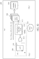
- FIG. 10 is a diagram illustrating a second integrated circuit design according to an embodiment of the present invention.
- the integrated circuit is a system-on-chip (SoC) 1000 having embedded memories included therein.
- SoC system-on-chip
- the SoC 1000 includes a clock tree 1002, a clock-gating cell circuit 1004, and one or more flip-flop circuits 1006. It should be noted that only the circuit elements pertinent to the present invention are shown in FIG. 10 . In practice, the SoC 1000 may have additional circuit elements to achieve other designated functions.
- the clock tree 1002 is arranged to distribute a plurality of clock signals to a plurality of clock-driven circuit elements in the SoC 1000, respectively.
- the clock tree 1002 may distribute a first clock signal CK_1 and a second clock signal CK_2 having the same frequency but different clock skews.
- Each flip-flop circuit 1006 may be a D-type flip flop (DFF) having a clock input port, a data input port and a data output port, where the clock input port is arranged to receive the first clock signal CK_1 from the clock tree 1002 via the clock-gating cell circuit 1004, the data input port is arranged to receive one non-clock signal Non_CK (e.g., a CS signal, a WE signal, a BYTE signal, an ADR bit, a DI bit, or any synchronous input), and the data output port is arranged to output the sampled non-clock signal Non_CK to the embedded memory 1008.
- DFF D-type flip flop
- the embedded memory 1008 has one interface pin arranged to receive the non-clock signal output from each flip-flop circuit 1006, and further has one interface pin arranged to receive the second clock signal CK_2 from the clock tree 1002. Specifically, the embedded memory 1008 performs memory access according to at least the second clock signal CK_2 received from the clock tree 1002 and the non-clock signal (s) Non_CK received from flip-flop circuit(s) 1006.
- the clock-gating cell circuit 1004 is arranged to receive the first clock signal CK_1 from the clock tree 1002, and selectively provide the first clock signal CK_1 to the clock input port of each flip-flop circuit 1006. As shown in FIG. 10 , the clock-gating cell circuit 1004 includes a clock-gating circuit 1010 and a programmable path delay circuit 1012. In this embodiment, the clock-gating circuit 1010 is a clock-gating cell implemented using a latch 1014 and a NAND gate 1016. The latch 1014 is controlled by the first clock signal CK_1 to output a clock-gating enable signal EN to one input port of the NAND gate 1016.
- the clock-gating enable signal EN When the clock-gating enable signal EN is set by a logic low level, the clock-gating function is enabled to gate the first clock signal CK_1, such that a constant voltage level is output from the clock-gating circuit 1010.
- the clock-gating enable signal EN When the clock-gating enable signal EN is set by a logic high level, the clock-gating function is disabled, thus allowing the first clock signal CK_1 to be output from the clock-gating circuit 1010.
- the NAND gate 1016 may be replaced with an AND gate, an OR gate or a NOR gate to meet the design requirements.
- the clock-gating circuit 1010 may be modified to include additional logic gates (e.g., inverters) to meet the design requirements To put it simply, the circuit design of the clock-gating circuit 1010 shown in FIG. 10 is for illustrative purposes only.
- the clock-gating circuit 1010 may be implemented using any available clock-gating design. Since the present invention does not focus on the circuit design of the clock-gating circuit 1010, further description is omitted here for brevity.
- the programmable path delay circuit 1012 receives the first clock signal CK_1 from the preceding clock-gating circuit 1010, and delivers the first clock signal CK_1 to each flip-flop circuit 1006 via a clock path 1011.
- the programmable path delay circuit 1012 is arranged to set a path delay of the clock path 1011 according to a setup-hold time control setting SHSEL.
- the programmable path delay circuit 1012 may be implemented using the programmable path delay circuit 112 shown in FIG. 2 with the first clock signal CK_1 shown in FIG. 10 as its clock input, or may be implemented using the programmable path delay circuit 112 shown in FIG.
- each flip-flop circuit 1006 may be a D-type flip flop (DFF) having a clock input port, a data input port, and a data output port, where the clock input port is arranged to receive the first clock signal CK_1 via the clock-gating cell circuit 1004, the data input port is arranged to receive one non-clock signal Non_CK (e.g., a CS signal, a WE signal, a BYTE signal, an ADR bit, a DI bit, or any synchronous input), and the data output port is arranged to output the sampled non-clock signal Non_CK to the embedded memory 1008.
- DFF D-type flip flop
- the setup-hold time control setting SHSEL With a proper setting of the setup-hold time control setting SHSEL, the timing of the first clock signal CK_1 fed into each flip-flop circuit 1006 is adjusted, thus affecting the timing of the non-clock signal Non_CK fed into the embedded memory 1008.
- the setup time and the hold time of the non-clock signal Non_CK received by the embedded memory 1008 can be indirectly programmed by the programmable path delay circuit 1012 of the clock-gating circuit 1004 external to the embedded memory 1008.
Landscapes
- Engineering & Computer Science (AREA)
- Microelectronics & Electronic Packaging (AREA)
- Computer Hardware Design (AREA)
- Physics & Mathematics (AREA)
- Theoretical Computer Science (AREA)
- Evolutionary Computation (AREA)
- Geometry (AREA)
- General Engineering & Computer Science (AREA)
- General Physics & Mathematics (AREA)
- Pulse Circuits (AREA)
- Design And Manufacture Of Integrated Circuits (AREA)
Abstract

Description
- This application claims the benefit of
U.S. provisional application No. 62/475,973, filed on 03/24/2017 - The present invention relates to an integrated circuit design, and more particularly, to an embedded memory with a setup-hold time that can be controlled internally or externally and an associated integrated circuit.
- In general, a system-on-chip (SoC) uses lots of embedded memories. In the SoC design phase, the traditional timing sign-off may reserve a 3-sigma local variation factor for hold-time margin. However, a defective parts per million (DPPM) level covered by 3-sigma is obviously smaller than 1000 DPPM. If the reserved hold-time margin is increased from 3-sigma to 6-7 sigma, the DPPM can be improved. However, the DPPM is improved at the expense of chip area, timing closure and speed performance. As a result, the SoC design suffers from chip area, timing closure and speed performance, inevitably. Further, in a silicon debug phase, the memory built-in self-test (MBIST) logic of the embedded memory is unable to identify hold-time violations at the memory input interface and the MBIST logic itself. This may result in holes in the MBIST Shmoo plot.
- One of the objectives of the claimed invention is to provide an embedded memory with a setup-hold time that can be controlled internally/externally and an associated integrated circuit.
- According to a first aspect of the present invention, an exemplary embedded memory in an integrated circuit is disclosed. The exemplary embedded memory includes a memory interface circuit, a cell array, and a peripheral circuit. The memory interface circuit includes a plurality of interface pins and a programmable path delay circuit. The interface pins are arranged to receive at least a clock signal, a non-clock signal, and a setup-hold time control setting. The programmable path delay circuit is arranged to set a path delay of at least one of a clock path and a non-clock path according to the setup-hold time control setting, wherein the clock path is arranged to deliver the clock signal, and the non-clock path is arranged to deliver the non-clock signal. The cell array has a plurality of memory cells. The peripheral circuit is arranged to access the cell array according to at least the clock signal provided from the clock path and the non-clock signal provided from the non-clock path.
- According to a second aspect of the present invention, an exemplary integrated circuit is disclosed. The exemplary integrated circuit includes a clock tree, a flip-flop circuit, an embedded memory, and a clock-gating cell circuit. The clock tree is arranged to distribute at least a first clock signal and a second clock signal. The flip-flop circuit has a clock input port and a data output port, wherein the clock input port is arranged to receive the first clock signal from the clock tree via the clock-gating cell circuit, and the data output port is arranged to output a non-clock signal. The embedded memory is arranged to receive the second clock signal from the clock tree, receive the non-clock signal from the flip-flop circuit, and perform memory access according to at least the second clock signal and the non-clock signal. The clock-gating cell circuit is arranged to receive the first clock signal, and selectively provide the first clock signal to the clock input port of the flip-flop circuit. The clock-gating cell circuit comprises a programmable path delay circuit arranged to set a path delay of a clock path according to a setup-hold time control setting, wherein the clock path is arranged to deliver the first clock signal.
- These and other objectives of the present invention will no doubt become obvious to those of ordinary skill in the art after reading the following detailed description of the preferred embodiment that is illustrated in the various figures and drawings.
-
-
FIG. 1 is a diagram illustrating a first integrated circuit design according to an embodiment of the present invention. -
FIG. 2 is a diagram illustrating a first exemplary design of a programmable path delay circuit shown inFIG. 1 according to an embodiment of the present invention. -
FIG. 3 is a diagram illustrating waveforms of a plurality of clock signals and a non-clock signal according to an embodiment of the present invention. -
FIG. 4 is a diagram illustrating a circuit design of a programmable path delay circuit shown inFIG. 2 according to an embodiment of the present invention. -
FIG. 5 is a diagram illustrating a second exemplary design of the programmable path delay circuit shown inFIG. 1 according to an embodiment of the present invention. -
FIG. 6 is a diagram illustrating a circuit design of a programmable path delay circuit shown inFIG. 5 according to an embodiment of the present invention. -
FIG. 7 is a diagram illustrating a third exemplary design of the programmable path delay circuit shown inFIG. 1 according to an embodiment of the present invention. -
FIG. 8 is a diagram illustrating waveforms of a plurality of non-clock signals and a clock signal according to an embodiment of the present invention. -
FIG. 9 is a diagram illustrating a fourth exemplary design of the programmable path delay circuit shown inFIG. 1 according to an embodiment of the present invention. -
FIG. 10 is a diagram illustrating a second integrated circuit design according to an embodiment of the present invention. - Certain terms are used throughout the following description and claims, which refer to particular components. As one skilled in the art will appreciate, electronic equipment manufacturers may refer to a component by different names. This document does not intend to distinguish between components that differ in name but not in function. In the following description and in the claims, the terms "include" and "comprise" are used in an open-ended fashion, and thus should be interpreted to mean "include, but not limited to ...". Also, the term "couple" is intended to mean either an indirect or direct electrical connection. Accordingly, if one device is coupled to another device, that connection may be through a direct electrical connection, or through an indirect electrical connection via other devices and connections.
- Embodiments of the present invention proposes an embedded memory with a setup-hold time that can be controlled internally or externally, thereby avoiding hold-time violations at the memory input interface. In this way, the "Shmoo hole" issue can be relaxed by the proposed solution. In addition, the SoC timing closure can also benefit from the proposed solution.
-
FIG. 1 is a diagram illustrating a first integrated circuit design according to an embodiment of the present invention. In this embodiment, the integrated circuit is a system-on-chip (SoC) 10 having embedded memories included therein. For clarity and simplicity, only one embeddedmemory 100 is illustrated. The embeddedmemory 100 includes acell array 102, aperipheral circuit 104, and amemory interface circuit 106. Thecell array 102 has a plurality ofmemory cells 108. Eachmemory cell 108 can be assessed by enabling one word line and one bit line at which thememory cell 108 is located. Theperipheral circuit 104 includes circuit elements needed to access (read/write) thecell array 102. For example, theperipheral circuit 104 may include a row decoder, row drivers, a clock generator, a timing controller, a column decoder, sense amplifiers, data latches, etc. In this embodiment, thememory interface circuit 106 includes a plurality ofinterface pins 110 and a programmablepath delay circuit 112. Theinterface pins 110 are arranged to receive a clock signal, a plurality of non-clock signals, and a delay selection signal. Specifically, theinterface pins 110 include one clock pin defined to receive a clock signal CK (which is an external clock generated from a clock source), one chip select (CS) pin defined to receive a CS signal (which is a non-clock signal), one write enable (WE) pin defined to receive a WE signal (which is a non-clock signal), one bit write enable (BYTE) pin defined to receive a BYTE signal (which is a non-clock signal), a plurality of address (ADR) pins defined to receive ADR bits (which are non-clock signals), a plurality of data input (DI) pins defined to receive DI bits (which are non-clock signals), and a plurality of delay select (DELSEL) pins defined to receive a delay selection signal composed of one or more DELSEL bits. It should be noted that a setup-hold time control setting SHSEL may be inputted by at least a portion (i.e., part or all) of the DELSEL bits, depending upon the actual design considerations. Theperipheral circuit 104 reads/writes thecell array 102 according to at least the clock signal CK provided from a clock path and non-clock signal (s) provided from non-clock path(s). Since an embodiment of the present invention focuses on the memory interface design (particularly, the programmable path delay circuit 112), further description ofcell array 102 andperipheral circuit 104 is omitted here for brevity. - It should be noted that only the circuit elements pertinent to the present invention are shown in
FIG. 1 . In practice, the embeddedmemory 100 may have additional circuit elements to achieve other designated functions. - The embedded
memory 100 has a programmable input path delay controlled by the programmablepath delay circuit 112. Hence, a programmable setup time and a programmable hold time of each non-clock signal received from an interface pin (e.g., a control pin, an address pin, or a data input pin) can be achieved at thememory interface circuit 106. - In accordance with one setup-hold time control scheme of the present invention, the programmable
path delay circuit 112 is arranged to set a path delay of a clock path according to the setup-hold time control setting SHSEL, where the clock path is used to deliver the clock signal CK received by oneinterface pin 110. -
FIG. 2 is a diagram illustrating a first exemplary design of the programmablepath delay circuit 112 shown inFIG. 1 according to an embodiment of the present invention. The programmablepath delay circuit 112 includes a plurality ofdelay cell circuits FIG. 2 and the number of multiplexers shown inFIG. 2 are for illustrative purposes only, and are not meant to be limitations of the present invention. In practice, the number of delay cell circuits and the number of multiplexers may be adjusted, depending upon actual design considerations. - The programmable
path delay circuit 112 receives the clock signal CK from oneinterface pin 110, and delivers the clock signal CK to eachlatch 202 in theperipheral circuit 104 via theclock path 204, where each of the latches 202 (e.g., latch[0]-latch[n]) receives one non-clock signal Non_CK received from oneinterface pin 110 and an internal clock signal Int_CK provided from the programmablepath delay circuit 112. By way of example, but not limitation, the non-clock signal Non_CK may be a CS signal, a WE signal, a BYTE signal, an ADR bit, a DI bit, or any synchronous input of the embeddedmemory 100. - Each of the
delay cell circuits delay cell circuits delay cell circuits - The
multiplexer 210 has an input port and an output port, wherein the input port is arranged to receive the clock signal CK without via any of thedelay cell circuits multiplexer 212 has an input port and an output port, wherein the input port is arranged to receive the clock signal CK via thedelay cell circuit 206, and the output port is arranged to selectively output the clock signal CK received at the input port according to the setup-hold time control setting SHSEL. Themultiplexer 214 has an input port and an output port, wherein the input port is arranged to receive the clock signal CK via thedelay cell circuits - In this embodiment, the setup-hold time control setting SHSEL determines which one of the
multiplexers following latch 202. When themultiplexer 210 is enabled by the setup-hold time control setting SHSEL, a clock signal CK1 (which is generated by passing the clock signal CK through the multiplexer 210) is used to act as the internal clock signal Int_CK. When themultiplexer 212 is enabled by the setup-hold time control setting SHSEL, a clock signal CK2 (which is generated by passing the clock signal CK through thedelay cell circuit 206 and the multiplexer 212) is used to act as the internal clock signal Int_CK. When themultiplexer 214 is enabled by the setup-hold time control setting SHSEL, a clock signal CK3 (which is generated by passing the clock signal CK through thedelay cell circuits path delay circuit 112, the path delay of theclock path 204 can be adjusted, thereby affecting the setup time and the hold time of the non-clock signal Non_CK with respect to the internal clock signal Int_CK (which may be regarded as a clock signal CK with a programmable memory interface delay). -
FIG. 3 is a diagram illustrating waveforms of clock signals CK, CK1, CK2, CK3 and non-clock signal Non_CK according to an embodiment of the present invention. The clock signals CK, CK1, CK2, CK3 have the same frequency but different phases. A phase delay between the clock signals CK1 and CK results from themultiplexer 210. A phase delay between the clock signals CK2 and CK results from thedelay cell circuit 206 and themultiplexer 212. A phase delay between the clock signals CK3 and CK results from thedelay cell circuits multiplexer 214. A setup time Tsetup is the amount of time the input signal should be held steady before a clock edge occurs. The hold time Thold is the amount of time the input signal should be held steady after the clock edge occurs. With a proper control of the programmablepath delay circuit 112, the timing of the clock edge of the internal clock signal Int_CK can be adjusted to avoid the setup time violation and/or the hold time violation of the non-clock signal Non_CK at thelatch 202. In this case shown inFIG. 3 , the hold time passes the timing requirement when the internal clock signal Int_CK is set by the clock signal CK1; the hold time marginally passes the timing requirement when the internal clock signal Int_CK is set by the clock signal CK2; and the hold time fails to pass the timing requirement when the internal clock signal Int_CK is set by the clock signal CK2. Preferably, the setup-hold time control setting SHSEL may be set to enable themultiplexer 210, thereby outputting the clock signal CK1 to thelatch 202. It should be noted that the waveforms shown inFIG. 3 are for illustrative purposes only, and are not meant to be limitations of the present invention. In practice, one of the clock signals CK1, CK2, CK3 may be selected on the basis of the actual timing relation between the clock signal CK and the non-clock signal Non_CK. -
FIG. 4 is a diagram illustrating a circuit design of the programmablepath delay circuit 112 shown inFIG. 2 according to an embodiment of the present invention. For clarity and simplicity, only twomultiplexers delay cell circuit 208 are shown inFIG. 4 . Thedelay cell circuit 208 is implemented using two inverters INV2 and INV3. Themultiplexer 210 is implemented using P-channel metal-oxide-semiconductor field effect transistors (PMOS transistors) MP1, MP2 and N-channel metal-oxide-semiconductor field effect transistors (NMOS transistors) MN1, MN2. Themultiplexer 212 is implemented using PMOS transistors MP3, MP4 and NMOS transistors MN3, MN4. The setup-hold time control setting SHSEL includes one control bit DELSEL. The inverter INV1 sets another control bit DELSELB by inverting a logic level of the control bit DELSEL. In other words, when the control bit DELSEL has a high logic value "1", the control bit DELSELB has a low logic value "0"; and when the control bit DELSEL has a low logic value "0", the control bit DELSELB has a high logic value "1". When the control bit DELSEL is set by the low logic value "0", themultiplexer 210 is enabled, while themultiplexer 212 is disabled. Hence, the clock signal CK passes through themultiplexer 210, and is further processed by an inverter INV4 to become the internal clock Int_CK. When the control bit DELSEL is set by the high logic value "1", themultiplexer 210 is disabled, while themultiplexer 212 is enabled. Hence, the clock signal CK passes through thedelay cell circuit 208 and themultiplexer 212, and is further processed by the inverter INV4 to become the internal clock signal Int_CK. It should be noted that the circuit implementation shown inFIG. 4 is for illustrative purposes only, and is not meant to be a limitation of the present invention. That is, the same objective of programming the path delay of theclock path 204 may be achieved by implementing the programmablepath delay circuit 112 shown inFIG. 2 with another circuit design. - As can be seen from
FIG. 4 , the path delay of theclock path 204 is programmed by an integer number of gate delays. Hence, the granularity of programming the path delay of theclock path 204 depends on the gate delay. To improve the granularity of programming the path delay of theclock path 204, the present invention proposes another design of the programmablepath delay circuit 112 shown inFIG. 1 . -
FIG. 5 is a diagram illustrating a second exemplary design of the programmablepath delay circuit 112 shown inFIG. 1 according to an embodiment of the present invention. The programmablepath delay circuit 112 includes abase delay circuit 502, a firstdelay control circuit 504, and a seconddelay control circuit 506. The programmablepath delay circuit 112 receives the clock signal CK from oneinterface pin 110, and delivers the clock signal CK to eachlatch 202 in theperipheral circuit 104 via aclock path 501, where each of thelatches 202 receives one non-clock signal Non_CK received from oneinterface pin 110 and an internal clock signal Int_CK provided from the programmablepath delay circuit 112. By way of example, but not limitation, the non-clock signal Non_CK may be a CS signal, a WE signal, a BYTE signal, an ADR bit, a DI bit, or any synchronous input of the embeddedmemory 100. - The
base delay circuit 502 is arranged to receive the clock signal CK, and apply a programmable delay amount to the clock signal CK. In other words, when the clock signal CK passes through thebase delay circuit 502, the clock signal CK is delayed by the programmable delay amount. The firstdelay control circuit 504 includes a plurality of first transistors M11-M1N connected in parallel between a first node N1 of thebase delay circuit 502 and a supply voltage VDD. The seconddelay control circuit 506 includes a plurality of second transistors M21-M2N connected in parallel between a second node N2 of thebase delay circuit 502 and a ground voltage GND. The number of first transistors M11-M1N implemented in the firstdelay control circuit 504 and the number of second transistors M21-M2N implemented in the seconddelay control circuit 506 may be adjusted, depending upon the actual design considerations. In this embodiment, the number of turned-on first transistors in the firstdelay control circuit 504 and the number of turned-on second transistors in the seconddelay control circuit 506 are both controlled by the setup-hold time control setting SHSEL. - The programmable delay amount of the
base delay circuit 502 is determined by the number of turned-on first transistors in the firstdelay control circuit 504 and the number of turned-on second transistors in the seconddelay control circuit 506. For example, the programmable delay amount of thebase delay circuit 502 is set by a first delay time when the number of turned-on first transistors in the firstdelay control circuit 504 is set by a first value and the number of turned-on second transistors in the seconddelay control circuit 506 is set by the same first value; and the programmable delay amount of thebase delay circuit 502 is set by a second delay time when the number of turned-on first transistors in the firstdelay control circuit 504 is set by a second value and the number of turned-on second transistors in the seconddelay control circuit 506 is set by the same second value. In this embodiment, if the first value is larger than the second value, the first delay time is shorter than the second delay time due to a larger driving current used by thebase delay circuit 502; and if the first value is smaller than the second value, the first delay time is longer than the second delay time due to a smaller driving current used by thebase delay circuit 502. With a proper control of the programmablepath delay circuit 112, the timing of the clock edge of the internal clock signal Int_CK can be adjusted to avoid the setup time violation and/or the hold time violation of the non-clock signal Non_CK at thelatch 202. - The programmable
path delay circuit 112 shown inFIG. 5 controls the path delay of theclock path 501 through tuning the magnitude of the driving current used by thebase delay circuit 502. Compared to the programmablepath delay circuit 112 shown inFIG. 2 , the programmablepath delay circuit 112 shown inFIG. 5 is capable of controlling the path delay with finer granularity. -
FIG. 6 is a diagram illustrating a circuit design of the programmablepath delay circuit 112 shown inFIG. 5 according to an embodiment of the present invention. The firstdelay control circuit 504 is implemented using PMOS transistors MP1, MP2, MP3. The seconddelay control circuit 506 is implemented using NMOS transistors MN1, MN2, MN3. For clarity and simplicity, each of the firstdelay control circuit 504 and the seconddelay control circuit 506 is shown having three transistors only. Thebase delay circuit 502 is implemented using PMOS transistors MP4, MP5 and NMOS transistors MN4, MN5, where PMOS transistor MP4 and NMOS transistor MN4 form one inverter, and PMOS transistor MP5 and NMOS transistor MN5 form another inverter. - The setup-hold time control setting SHSEL includes one control input DELSEL composed of two control bits DELSEL[0] and DELSEL[1]. The inverter INV1 sets another control bit DELSEL[0]B by inverting a logic level of the control bit DELSEL[0]. The inverter INV2 sets yet another control bit DELSEL[1]B by inverting a logic level of the control bit DELSEL[1]. In other words, when the control bit DELSEL[0] has a high logic value "1", the control bit DELSEL[0]B has a low logic value "0"; and when the control bit DELSEL[0] has a low logic value "0", the control bit DELSEL[0]B has a high logic value "1". Similarly, when the control bit DELSEL[1] has a high logic value "1", the control bit DELSEL[1]B has a low logic value "0"; and when the control bit DELSEL[1] has a low logic value "0", the control bit DELSEL[1]B has a high logic value "1". It should be noted that the PMOS transistor MP3 is turned on by a first bias voltage VB1 (e.g., ground voltage GND), and the NMOS transistor NP3 is turned on by a second bias voltage VB2 (e.g., supply voltage VDD). Thus, the PMOS transistor MP3 is turned on regardless of on/off statuses of PMOS transistors MP1 and MP2, and the NMOS transistor MN3 is turned on regardless of on/off statuses of NMOS transistors MN1 and MN2.
- When the control bit DELSEL[0] is set by the low logic value "0", the PMOS transistor MP1 is turned off, and the NMOS transistor MN1 is turned off. When the control bit DELSEL[0] is set by the high logic value "1", the PMOS transistor MP1 is turned on, and the NMOS transistor MN1 is turned on. When the control bit DELSEL[1] is set by the low logic value "0", the PMOS transistor MP2 is turned off, and the NMOS transistor MN2 is turned off. When the control bit DELSEL[1] is set by the high logic value "1", the PMOS transistor MP2 is turned on, and the NMOS transistor MN2 is turned on.
- When the control bits DELSEL[0] and DELSEL[1] are both set by the low logic value "0", the first
delay control circuit 504 has only one turned-on PMOS transistor MP3, and the seconddelay control circuit 506 has only one turned-on NMOS transistor MN3. Hence, the path delay of theclock path 204 is programmed to have a largest delay amount due to a smallest driving current. - When only one of the control bit DELSEL[0] and DELSEL[1] is set by the high logic value "1", the first
delay control circuit 504 has two turned-on PMOS transistors (e.g., MP1 and MP3, or MP2 and MP3), and the seconddelay control circuit 506 has two turned-on NMOS transistors (e.g., MN1 and MN3, or MN2 and MN3). Hence, the path delay of theclock path 204 is programmed to have a medium delay amount due to a medium driving current. - When the control bit DELSEL[0] and DELSEL[1] are both set by the high logic value "1", the first
delay control circuit 504 has three turned-on PMOS transistors MP1, MP2, MP3, and the seconddelay control circuit 506 has three turned-on NMOS transistors MN1, MN2, MN3. Hence, the path delay of theclock path 204 is programmed to have a smallest delay amount due to a largest driving current. - It should be noted that the circuit implementation shown in
FIG. 6 is for illustrative purposes only, and is not meant to be a limitation of the present invention. That is, the same objective of programming the path delay of theclock path 501 may be achieved by implementing the programmablepath delay circuit 112 shown inFIG. 5 with another circuit design. - As can be known from
FIG. 3 , whether any of the setup time Tsetup and the hold time Thold violates the timing requirement depends on the relative timing relation between a clock signal and a non-clock signal (which is to be sampled by the clock signal). Adjusting the timing of the clock signal is able to affect the setup time Tsetup and the hold time Thold. Alternatively, adjusting the timing of the non-clock signal is also able to affect the setup time Tsetup and the hold time Thold. In accordance with another setup-hold time control scheme of the present invention, the programmablepath delay circuit 112 is arranged to set a path delay of a non-clock path according to the setup-hold time control setting SHSEL, where the non-clock path is used to deliver a non-clock signal (e.g., a CS signal, a WE signal, a BYTE signal, an ADR bit, a DI bit, or any synchronous input) received by oneinterface pin 110 of the embeddedmemory 100. -
FIG. 7 is a diagram illustrating a third exemplary design of the programmablepath delay circuit 112 shown inFIG. 1 according to an embodiment of the present invention. The programmablepath delay circuit 112 may include a plurality ofcircuit modules 702, each arranged to provide one non-clock signal Non_CK to one of a plurality oflatches 202 in theperipheral circuit 104. Eachcircuit module 702 in the programmablepath delay circuit 112 includes a plurality ofdelay cell circuits FIG. 7 and the number of multiplexers shown inFIG. 7 are for illustrative purposes only, and are not meant to be limitations of the present invention. In practice, the number of delay cell circuits and the number of multiplexers implemented in eachcircuit module 702 may be adjusted, depending upon the actual design considerations. - Each
circuit module 702 of the programmablepath delay circuit 112 receives the non-clock signal Non_CK (e.g., a CS signal, a WE signal, a BYTE signal, an ADR bit, a DI bit, or any synchronous input of the embedded memory 100) from oneinterface pin 110, and delivers the non-clock signal Non_CK to onelatch 202 via anon-clock path 704, where eachlatch 202 receives the clock signal CK received from oneinterface pin 110 and one non-clock signal Non_CK provided from the programmablepath delay circuit 112. - Each of the
delay cell circuits delay cell circuits delay cell circuits - The
multiplexer 710 has an input port and an output port, wherein the input port is arranged to receive the non-clock signal Non_CK without via any of thedelay cell circuits multiplexer 712 has an input port and an output port, wherein the input port is arranged to receive the non-clock signal Non_CK via thedelay cell circuit 706, and the output port is arranged to selectively output the non-clock signal Non_CK received at the input port according to the setup-hold time control setting SHSEL. Themultiplexer 714 has an input port and an output port, wherein the input port is arranged to receive the non-clock signal Non_CK via thedelay cell circuits - In this embodiment, the setup-hold time control setting SHSEL determines which one of the
multiplexers following latch 202. When themultiplexer 710 is enabled by the setup-hold time control setting SHSEL, a non-clock signal Non_CK1 (which is generated by passing the non-clock signal Non_CK through the multiplexer 710) is used to act as the non-clock input of thelatch 202. When themultiplexer 712 is enabled by the setup-hold time control setting SHSEL, a non-clock signal Non_CK2 (which is generated by passing the non-clock signal Non_CK through thedelay cell circuit 706 and the multiplexer 712) is used to act as the non-clock input of thelatch 202. When themultiplexer 714 is enabled by the setup-hold time control setting SHSEL, a non-clock signal Non_CK3 (which is generated by passing the non-clock signal Non_CK through thedelay cell circuits latch 202. With a proper control of the programmablepath delay circuit 112, the path delay of thenon-clock path 704 can be adjusted, thereby affecting the setup time and the hold time of the non-clock input (which may be regarded as a non-clock signal Non_CK with a programmable memory interface delay) with respect to the clock signal CK. -
FIG. 8 is a diagram illustrating waveforms of non-clock signals Non_CK, Non_CK1, Non_CK2, Non_CK3 and clock signal CK according to an embodiment of the present invention. The non-clock signals Non_CK, Non_CK1, Non_CK2, Non_CK3 have the same waveform but different timing. A timing delay between the non-clock signals Non_CK1 and Non_CK results from themultiplexer 710. A timing delay between the non-clock signals Non_CK2 and Non_CK results from thedelay cell circuit 706 and themultiplexer 712. A timing delay between the non-clock signals Non_CK3 and Non_CK results from thedelay cell circuits multiplexer 714. With a proper control of the programmablepath delay circuit 112, the timing of the non-clock input can be adjusted to avoid the setup time violation and/or the hold time violation of the non-clock signal Non_CK at thelatch 202. In this case shown inFIG. 8 , the setup time passes the timing requirement when the non-clock input is set by the non-clock signal Non_CK1; the setup time marginally passes the timing requirement when the non-clock input is set by the non-clock signal Non_CK2; and the setup time fails to pass the timing requirement when the non-clock input is set by the non-clock signal Non_CK3. Preferably, the setup-hold time control setting SHSEL may be set to enable themultiplexer 710, thereby outputting the non-clock signal Non_CK1 to thelatch 202. It should be noted that the waveforms shown inFIG. 8 are for illustrative purposes only, and are not meant to be limitations of the present invention. In practice, one of the non-clock signals Non_CK1, Non_CK2, Non_CK3 may be selected on the basis of the actual timing relation between the clock signal CK and the non-clock signal Non_CK. - The function of each
circuit module 702 in the programmablepath delay circuit 112 shown inFIG. 7 is similar to that of the programmablepath delay circuit 112 shown inFIG. 2 . The major difference is that an input of eachcircuit module 702 in the programmablepath delay circuit 112 shown inFIG. 7 is a non-clock signal Non_CK (e.g., a CS signal, a WE signal, a BYTE signal, an ADR bit, a DI bit, or any synchronous input). Hence, eachcircuit module 702 in the programmablepath delay circuit 112 may also be implemented using the circuit design shown inFIG. 4 . Further description is omitted here for brevity. -
FIG. 9 is a diagram illustrating a fourth exemplary design of the programmablepath delay circuit 112 shown inFIG. 1 according to an embodiment of the present invention. The programmablepath delay circuit 112 may include a plurality ofcircuit modules 902, each arranged to receive a non-clock signal Non_CK from oneinterface pin 110 and deliver the non-clock signal Non_CK to onelatch 202 in theperipheral circuit 104 via anon-clock path 901. Eachcircuit module 902 in the programmablepath delay circuit 112 includes abase delay circuit 902, a firstdelay control circuit 904, and a seconddelay control circuit 906. Eachlatch 202 receives the clock signal CK from oneinterface pin 110 and one non-clock signal Non_CK provided from the programmablepath delay circuit 112. By way of example, but not limitation, the non-clock signal Non_CK may be a CS signal, a WE signal, a BYTE signal, an ADR bit, a DI bit, or any synchronous input of the embeddedmemory 100. - The
base delay circuit 902 is arranged to receive the non-clock signal Non_CK, and apply a programmable delay amount to the non-clock signal Non_CK. In other words, when the non-clock signal Non_CK passes through thebase delay circuit 902, the non-clock signal Non_CK is delayed by the programmable delay amount. The firstdelay control circuit 904 includes a plurality of first transistors M11-M1N connected in parallel between a first node N1 of thebase delay circuit 902 and a supply voltage VDD. The seconddelay control circuit 906 includes a plurality of second transistors M21-M2N connected in parallel between a second node N2 of thebase delay circuit 902 and a ground voltage GND. The number of first transistors M11-M1N implemented in the firstdelay control circuit 904 and the number of second transistors M21-M2N implemented in the seconddelay control circuit 906 may be adjusted, depending upon the actual design considerations. In this embodiment, the number of turned-on first transistors in the firstdelay control circuit 904 and the number of turned-on second transistors in the seconddelay control circuit 906 are both controlled by the setup-hold time control setting SHSEL. - The programmable delay amount of the
base delay circuit 902 is determined by the number of turned-on first transistors in the firstdelay control circuit 904 and the number of turned-on second transistors in the seconddelay control circuit 906. For example, the programmable delay amount of thebase delay circuit 902 is set by a first delay time when the number of turned-on first transistors in the firstdelay control circuit 904 is set by a first value and the number of turned-on second transistors in the seconddelay control circuit 906 is set by the same first value; and the programmable delay amount of thebase delay circuit 902 is set by a second delay time when the number of turned-on first transistors in the firstdelay control circuit 904 is set by a second value and the number of turned-on second transistors in the seconddelay control circuit 906 is set by the same second value. In this embodiment, if the first value is larger than the second value, the first delay time is shorter than the second delay time due to a larger driving current used by thebase delay circuit 902; and if the first value is smaller than the second value, the first delay time is longer than the second delay time due to a smaller driving current used by thebase delay circuit 902. With a proper control of the programmablepath delay circuit 112, the timing of the non-clock input can be adjusted to avoid the setup time violation and/or the hold time violation of the non-clock input at thelatch 202. - The programmable
path delay circuit 112 shown inFIG. 9 controls the path delay of theclock path 901 through tuning the magnitude of the driving current used by thebase delay circuit 902. Compared to the programmablepath delay circuit 112 shown inFIG. 7 , the programmablepath delay circuit 112 shown inFIG. 9 is capable of controlling the path delay with finer granularity. - The function of each
circuit module 902 in the programmablepath delay circuit 112 shown inFIG. 9 is similar to that of the programmablepath delay circuit 112 shown inFIG. 5 . The major difference is that an input of eachcircuit module 902 in the programmablepath delay circuit 112 shown inFIG. 9 is a non-clock signal Non_CK (e.g., a CS signal, a WE signal, a BYTE signal, an ADR bit, a DI bit, or any synchronous input). Hence, eachcircuit module 902 in the programmablepath delay circuit 112 may also be implemented using the circuit design shown inFIG. 6 . Further description is omitted here for brevity. - In above embodiments, the programmable
path delay circuit 112 is used to set a path delay of only one of a clock path and a non-clock path according to the setup-hold time control setting. Alternatively, the programmablepath delay circuit 112 may be modified to set path delays of both of a clock path and a non-clock path according to the setup-hold time control setting. This alternative design also falls within the scope of the present invention. - Adjusting the timing of the non-clock signal is also able to affect the setup time Tsetup and the hold time Thold. In above embodiments, the embedded
memory 100 has thememory interface circuit 106 equipped with the programmablepath delay circuit 112 for achieving the objective of adjusting the timing of the non-clock signal at the memory interface. In other words, the above embodiments propose an embedded memory with a setup-hold time controlled internally. However, the same objective of adjusting the timing of a non-clock signal may be achieved by adjusting the timing of a clock signal at a circuit element (e.g., a flip flop) that is external to an embedded memory and is used to provide the non-clock signal to the embedded memory. Hence, an embodiment of the present invention further proposes an embedded memory with a setup-hold time controlled externally. -
FIG. 10 is a diagram illustrating a second integrated circuit design according to an embodiment of the present invention. In this embodiment, the integrated circuit is a system-on-chip (SoC) 1000 having embedded memories included therein. For clarity and simplicity, only one embeddedmemory 1008 is illustrated. In addition to the embeddedmemory 1008, theSoC 1000 includes a clock tree 1002, a clock-gatingcell circuit 1004, and one or more flip-flop circuits 1006. It should be noted that only the circuit elements pertinent to the present invention are shown inFIG. 10 . In practice, theSoC 1000 may have additional circuit elements to achieve other designated functions. - The clock tree 1002 is arranged to distribute a plurality of clock signals to a plurality of clock-driven circuit elements in the
SoC 1000, respectively. For example, the clock tree 1002 may distribute a first clock signal CK_1 and a second clock signal CK_2 having the same frequency but different clock skews. Each flip-flop circuit 1006 may be a D-type flip flop (DFF) having a clock input port, a data input port and a data output port, where the clock input port is arranged to receive the first clock signal CK_1 from the clock tree 1002 via the clock-gatingcell circuit 1004, the data input port is arranged to receive one non-clock signal Non_CK (e.g., a CS signal, a WE signal, a BYTE signal, an ADR bit, a DI bit, or any synchronous input), and the data output port is arranged to output the sampled non-clock signal Non_CK to the embeddedmemory 1008. The embeddedmemory 1008 has one interface pin arranged to receive the non-clock signal output from each flip-flop circuit 1006, and further has one interface pin arranged to receive the second clock signal CK_2 from the clock tree 1002. Specifically, the embeddedmemory 1008 performs memory access according to at least the second clock signal CK_2 received from the clock tree 1002 and the non-clock signal (s) Non_CK received from flip-flop circuit(s) 1006. - The clock-gating
cell circuit 1004 is arranged to receive the first clock signal CK_1 from the clock tree 1002, and selectively provide the first clock signal CK_1 to the clock input port of each flip-flop circuit 1006. As shown inFIG. 10 , the clock-gatingcell circuit 1004 includes a clock-gating circuit 1010 and a programmable path delay circuit 1012. In this embodiment, the clock-gating circuit 1010 is a clock-gating cell implemented using alatch 1014 and aNAND gate 1016. Thelatch 1014 is controlled by the first clock signal CK_1 to output a clock-gating enable signal EN to one input port of theNAND gate 1016. When the clock-gating enable signal EN is set by a logic low level, the clock-gating function is enabled to gate the first clock signal CK_1, such that a constant voltage level is output from the clock-gating circuit 1010. When the clock-gating enable signal EN is set by a logic high level, the clock-gating function is disabled, thus allowing the first clock signal CK_1 to be output from the clock-gating circuit 1010. - In some embodiments of the present invention, the
NAND gate 1016 may be replaced with an AND gate, an OR gate or a NOR gate to meet the design requirements. Further, the clock-gating circuit 1010 may be modified to include additional logic gates (e.g., inverters) to meet the design requirements To put it simply, the circuit design of the clock-gating circuit 1010 shown inFIG. 10 is for illustrative purposes only. The clock-gating circuit 1010 may be implemented using any available clock-gating design. Since the present invention does not focus on the circuit design of the clock-gating circuit 1010, further description is omitted here for brevity. - When the clock-gating function is disabled by the clock-gating enable signal EN, the programmable path delay circuit 1012 receives the first clock signal CK_1 from the preceding clock-
gating circuit 1010, and delivers the first clock signal CK_1 to each flip-flop circuit 1006 via aclock path 1011. The programmable path delay circuit 1012 is arranged to set a path delay of theclock path 1011 according to a setup-hold time control setting SHSEL. For example, the programmable path delay circuit 1012 may be implemented using the programmablepath delay circuit 112 shown inFIG. 2 with the first clock signal CK_1 shown inFIG. 10 as its clock input, or may be implemented using the programmablepath delay circuit 112 shown inFIG. 4 with the first clock signal CK_1 shown inFIG. 10 as its clock input. Since a person skilled in the art can readily understand details of the programmable path delay circuit 1012 after reading above paragraphs directed to the programmablepath delay circuit 112 shown inFIG. 2 andFIG. 4 , further description is omitted here for brevity. - As mentioned above, each flip-
flop circuit 1006 may be a D-type flip flop (DFF) having a clock input port, a data input port, and a data output port, where the clock input port is arranged to receive the first clock signal CK_1 via the clock-gatingcell circuit 1004, the data input port is arranged to receive one non-clock signal Non_CK (e.g., a CS signal, a WE signal, a BYTE signal, an ADR bit, a DI bit, or any synchronous input), and the data output port is arranged to output the sampled non-clock signal Non_CK to the embeddedmemory 1008. With a proper setting of the setup-hold time control setting SHSEL, the timing of the first clock signal CK_1 fed into each flip-flop circuit 1006 is adjusted, thus affecting the timing of the non-clock signal Non_CK fed into the embeddedmemory 1008. Hence, the setup time and the hold time of the non-clock signal Non_CK received by the embedded memory 1008 (which further receives the second clock signal CK_2) can be indirectly programmed by the programmable path delay circuit 1012 of the clock-gating circuit 1004 external to the embeddedmemory 1008. - Those skilled in the art will readily observe that numerous modifications and alterations of the device and method may be made while retaining the teachings of the invention. Accordingly, the above disclosure should be construed as limited only by the metes and bounds of the appended claims.
Claims (14)
- An embedded memory (100) in an integrated circuit (10) comprising:a memory interface circuit (106), comprising:a plurality of interface pins (110), arranged to receive at least a clock signal, a non-clock signal, and a setup-hold time control setting; anda programmable path delay circuit (112), arranged to set a path delay of at least one of a clock path and a non-clock path according to the setup-hold time control setting, wherein the clock path is arranged to deliver the clock signal, and the non-clock path is arranged to deliver the non-clock signal;a cell array (102), comprising a plurality of memory cells (108); anda peripheral circuit (104), arranged to access the cell array (102) according to at least the clock signal provided from the clock path circuit and the non-clock signal provided from the non-clock path.
- The embedded memory (100) of claim 1, wherein the programmable path delay circuit (112)is arranged to control the path delay of the clock path according to the setup-hold time control setting.
- The embedded memory (100) of claim 2, wherein the programmable path delay circuit (112) comprises:a delay cell circuit (206, 208), arranged to apply a predetermined delay amount to the clock signal;a first multiplexer (210, 212, 214), having a first input port and a first output port, wherein the first input port is arranged to receive the clock signal without via the delay cell circuit (206, 208), and the first output port is arranged to selectively output the clock signal received at the first input port according to the setup-hold time control setting; anda second multiplexer (210, 212, 214), having a second input port and a second output port, wherein the second input port is arranged to receive the clock signal via the delay cell circuit (206, 208), and the second output port is arranged to selectively output the clock signal received at the second input port according to the setup-hold time control setting.
- The embedded memory (100) of claim 2, wherein the programmable path delay circuit (112) comprises:a base delay circuit(502), arranged to receive the clock signal, and apply a programmable delay amount to the clock signal;a first delay control circuit (504), comprising a plurality of first transistors connected in parallel between a first node of the base delay circuit (502) and a supply voltage, wherein a number of turned-on first transistors in the first delay control circuit (504)is controlled by the setup-hold time control setting; anda second delay control circuit (506), comprising a plurality of second transistors connected in parallel between a second node of the base delay circuit (502)and a ground voltage, wherein a number of turned-on second transistors in the second delay control circuit (506) is controlled by the setup-hold time control setting;wherein the programmable delay amount is set by the number of turned-on first transistors in the first delay control circuit (504) and the number of turned-on second transistors in the second delay control circuit (506).
- The embedded memory (100) of claim 1, wherein the programmable path delay circuit (112) is arranged to control the path delay of the non-clock path according to the setup-hold time control setting.
- The embedded memory (100) of claim 5, wherein the programmable path delay circuit (112) comprises:a delay cell circuit (206, 208), arranged to apply a predetermined delay amount to the non-clock signal;a first multiplexer (210, 212, 214), having a first input port and a first output port, wherein the first input port is arranged to receive the non-clock signal without via the delay cell circuit (206, 208), and the first output port is arranged to selectively output the non-clock signal received at the first input port according to the setup-hold time control setting; anda second multiplexer (210, 212, 214), having a second input port and a second output port, wherein the second input port is arranged to receive the non-clock signal via the delay cell circuit (206, 208), and the second output port is arranged to selectively output the non-clock signal received at the second input port according to the setup-hold time control setting.
- The embedded memory (100) of claim 5, wherein the programmable path delay circuit (112) comprises:a base delay circuit (502), arranged to receive the non-clock signal, and apply a programmable delay amount to the non-clock signal;a first delay control circuit (504), comprising a plurality of first transistors connected in parallel between a first node of the base delay circuit(502) and a supply voltage, wherein a number of turned-on first transistors in the first delay control circuit (504) is controlled by the setup-hold time control setting; anda second delay control circuit (506), comprising a plurality of second transistors connected in parallel between a second node of the base delay circuit (502) and a ground voltage, wherein a number of turned-on second transistors in the second delay control circuit (506) is controlled by the setup-hold time control setting;wherein the programmable delay amount is set by the number of turned-on first transistors in the first delay control circuit (504) and the number of turned-on second transistors in the second delay control circuit (506).
- The embedded memory (100) of claim 5, wherein the non-clock signal is a control input received from a control pin included in the interface pins (110).
- The embedded memory (100) of claim 5, wherein the non-clock signal is an address bit received from an address pin included in the interface pins (110).
- The embedded memory (100) of claim 5, wherein the non-clock signal is a data bit received from a data input pin included in the interface pins (110).
- An integrated circuit (1000) comprising:a clock tree (1002), arranged to distribute at least a first clock signal and a second clock signal;a flip-flop circuit (1006), having a clock input port and a data output port, wherein the clock input port is arranged to receive the first clock signal from the clock tree via a clock-gating cell circuit (1004), and the data output port is arranged to output a non-clock signal;an embedded memory (1008), arranged to receive the second clock signal from the clock tree (1002), receive the non-clock signal from the flip-flop circuit (1006), and perform memory access according to at least the second clock signal and the non-clock signal; andthe clock-gating cell circuit (1004), arranged to receive the first clock signal, and selectively provide the first clock signal to the clock input port of the flip-flop circuit (1006), wherein the clock-gating cell circuit (1004) comprises:a programmable path delay circuit (1012), arranged to set a path delay of a clock path according to a setup-hold time control setting, wherein the clock path is arranged to deliver the first clock signal.
- The integrated circuit (1000) of claim 11, wherein the non-clock signal received by the embedded memory is a control input; or
wherein the non-clock signal received by the embedded memory is an address bit; or
wherein the non-clock signal received by the embedded memory is a data bit. - The integrated circuit (1000)of claim 11 or claim 12, wherein the programmable path delay circuit (1012) comprises:a delay cell circuit (206, 208), arranged to apply a predetermined delay amount to the first clock signal;a first multiplexer (210, 212, 214), having a first input port and a first output port, wherein the first input port is arranged to receive the first clock signal without via the delay cell circuit (206, 208), and the first output port is arranged to selectively output the first clock signal received at the first input port according to the setup-hold time control setting; anda second multiplexer (210, 212, 214), having a second input port and a second output port, wherein the second input port is arranged to receive the first clock signal via the delay cell circuit (206, 208), and the second output port is arranged to selectively output the first clock signal received at the second input port according to the setup-hold time control setting.
- The integrated circuit of claim 11 or claim 12, wherein the programmable path delay circuit (1012) comprises:a base delay circuit (502), arranged to receive the first clock signal, and apply a programmable delay amount to the first clock signal;a first delay control circuit (504), comprising a plurality of first transistors connected in parallel between a first node of the base delay circuit (502) and a supply voltage, wherein a number of turned-on first transistors in the first delay control circuit (504) is controlled by the setup-hold time control setting; anda second delay control circuit (506), comprising a plurality of second transistors connected in parallel between a second node of the base delay circuit (502) and a ground voltage, wherein a number of turned-on second transistors in the second delay control circuit (506) is controlled by the setup-hold time control setting;wherein the programmable delay amount is set by the number of turned-on first transistors in the first delay control circuit (504) and the number of turned-on second transistors in the second delay control circuit (506).
Applications Claiming Priority (2)
| Application Number | Priority Date | Filing Date | Title |
|---|---|---|---|
| US201762475973P | 2017-03-24 | 2017-03-24 | |
| US15/818,768 US10332574B2 (en) | 2017-03-24 | 2017-11-21 | Embedded memory with setup-hold time controlled internally or externally and associated integrated circuit |
Publications (2)
| Publication Number | Publication Date |
|---|---|
| EP3379538A1 true EP3379538A1 (en) | 2018-09-26 |
| EP3379538B1 EP3379538B1 (en) | 2020-11-25 |
Family
ID=60915235
Family Applications (1)
| Application Number | Title | Priority Date | Filing Date |
|---|---|---|---|
| EP17208158.0A Active EP3379538B1 (en) | 2017-03-24 | 2017-12-18 | Embedded memory with setup-hold time controlled internally or externally and associated integrated circuit |
Country Status (4)
| Country | Link |
|---|---|
| US (1) | US10332574B2 (en) |
| EP (1) | EP3379538B1 (en) |
| CN (1) | CN108630258B (en) |
| TW (1) | TWI644311B (en) |
Families Citing this family (8)
| Publication number | Priority date | Publication date | Assignee | Title |
|---|---|---|---|---|
| US10776550B1 (en) * | 2019-04-14 | 2020-09-15 | Mediatek Inc. | Integrated circuit having timing fixing circuit that introduces no short-circuit current under normal operation and associated timing fixing cell in cell library |
| CN110780646B (en) * | 2019-09-21 | 2021-11-26 | 苏州浪潮智能科技有限公司 | Memory quality early warning method based on MES system |
| US11386250B2 (en) * | 2020-01-28 | 2022-07-12 | Synopsys, Inc. | Detecting timing violations in emulation using field programmable gate array (FPGA) reprogramming |
| US11757439B2 (en) * | 2021-02-02 | 2023-09-12 | Efinix, Inc. | Chained programmable delay elements |
| JP2022146532A (en) * | 2021-03-22 | 2022-10-05 | キオクシア株式会社 | Memory system and delay control method |
| CN115906722B (en) * | 2021-08-16 | 2025-09-09 | 富联精密电子(天津)有限公司 | Server system and method for improving pin multiplexing rate of programmable device |
| TWI799249B (en) * | 2022-04-29 | 2023-04-11 | 瑞昱半導體股份有限公司 | Testing circuitry for testing multicycle path circuit |
| CN117074901A (en) * | 2022-05-10 | 2023-11-17 | 瑞昱半导体股份有限公司 | Test circuit system for testing multi-cycle path circuits |
Citations (3)
| Publication number | Priority date | Publication date | Assignee | Title |
|---|---|---|---|---|
| US20110187433A1 (en) * | 2010-01-29 | 2011-08-04 | Infineon Technologies Ag | On-Chip Self Calibrating Delay Monitoring Circuitry |
| US8514002B2 (en) * | 2010-04-02 | 2013-08-20 | Renesas Electronics Corporation | Clock delay adjustment circuit for semiconductor integrated circuit and control method of the same |
| US20160191031A1 (en) * | 2014-08-05 | 2016-06-30 | Apple Inc. | Dynamic margin tuning for controlling custom circuits and memories |
Family Cites Families (14)
| Publication number | Priority date | Publication date | Assignee | Title |
|---|---|---|---|---|
| US5444405A (en) | 1992-03-02 | 1995-08-22 | Seiko Epson Corporation | Clock generator with programmable non-overlapping clock edge capability |
| US5452239A (en) | 1993-01-29 | 1995-09-19 | Quickturn Design Systems, Inc. | Method of removing gated clocks from the clock nets of a netlist for timing sensitive implementation of the netlist in a hardware emulation system |
| US6310506B1 (en) | 1996-10-29 | 2001-10-30 | Texas Instruments Incorporated | Programmable setup/hold time delay network |
| KR100317317B1 (en) | 1998-12-31 | 2002-01-16 | 김영환 | Circuit for inputing control signal of semiconductor device |
| KR100415193B1 (en) | 2001-06-01 | 2004-01-16 | 삼성전자주식회사 | internal clock generating method in semiconductor memory device and circuit therefore |
| KR100506063B1 (en) | 2002-12-21 | 2005-08-05 | 주식회사 하이닉스반도체 | Apparatus for controlling setup/hold time |
| KR20070016857A (en) * | 2005-08-05 | 2007-02-08 | 주식회사 하이닉스반도체 | Setup hold time control circuit |
| US7865756B2 (en) | 2007-03-12 | 2011-01-04 | Mosaid Technologies Incorporated | Methods and apparatus for clock signal synchronization in a configuration of series-connected semiconductor devices |
| CN100533600C (en) * | 2007-03-14 | 2009-08-26 | 北京中星微电子有限公司 | Device and method for verifying synchronous memory controller based on field programmable gate array |
| KR100956782B1 (en) * | 2008-09-24 | 2010-05-12 | 주식회사 하이닉스반도체 | Setup / hold time test device and method |
| US8887019B2 (en) * | 2010-11-16 | 2014-11-11 | Cadence Design Systems, Inc. | Method and system for providing efficient on-product clock generation for domains compatible with compression |
| US9123438B2 (en) | 2013-10-15 | 2015-09-01 | Nvidia Corporation | Configurable delay circuit and method of clock buffering |
| US9684622B2 (en) * | 2014-06-09 | 2017-06-20 | Micron Technology, Inc. | Method and apparatus for controlling access to a common bus by multiple components |
| CN105976857A (en) * | 2016-05-20 | 2016-09-28 | 西安紫光国芯半导体有限公司 | Signal establishing time control circuit and dynamic storage based on same |
-
2017
- 2017-11-21 US US15/818,768 patent/US10332574B2/en active Active
- 2017-12-18 EP EP17208158.0A patent/EP3379538B1/en active Active
-
2018
- 2018-03-14 TW TW107108574A patent/TWI644311B/en not_active IP Right Cessation
- 2018-03-15 CN CN201810213231.9A patent/CN108630258B/en active Active
Patent Citations (3)
| Publication number | Priority date | Publication date | Assignee | Title |
|---|---|---|---|---|
| US20110187433A1 (en) * | 2010-01-29 | 2011-08-04 | Infineon Technologies Ag | On-Chip Self Calibrating Delay Monitoring Circuitry |
| US8514002B2 (en) * | 2010-04-02 | 2013-08-20 | Renesas Electronics Corporation | Clock delay adjustment circuit for semiconductor integrated circuit and control method of the same |
| US20160191031A1 (en) * | 2014-08-05 | 2016-06-30 | Apple Inc. | Dynamic margin tuning for controlling custom circuits and memories |
Also Published As
| Publication number | Publication date |
|---|---|
| US10332574B2 (en) | 2019-06-25 |
| CN108630258A (en) | 2018-10-09 |
| US20180277179A1 (en) | 2018-09-27 |
| EP3379538B1 (en) | 2020-11-25 |
| TW201835914A (en) | 2018-10-01 |
| TWI644311B (en) | 2018-12-11 |
| CN108630258B (en) | 2020-11-20 |
Similar Documents
| Publication | Publication Date | Title |
|---|---|---|
| EP3379538B1 (en) | Embedded memory with setup-hold time controlled internally or externally and associated integrated circuit | |
| US7411852B2 (en) | Semiconductor memory device and method of adjusting same | |
| US9837131B2 (en) | Semiconductor device and output circuit thereof | |
| US7977977B1 (en) | Dynamic logic circuit with device to prevent contention between pull-up and pull-down device | |
| CN110603591B (en) | Apparatus and method for configurable command and data input circuit for semiconductor memory | |
| JP4434858B2 (en) | Duty correction voltage generation circuit and duty correction voltage generation method | |
| KR20190065137A (en) | Driving circuit, semiconductor device including the same, and control method of the driving circuit | |
| US9196330B2 (en) | Mimicking multi-voltage domain wordline decoding logic for a memory array | |
| KR102583438B1 (en) | Systems and methods for controlling power assertion in a memory device | |
| US6249461B1 (en) | Flash memory device with a status read operation | |
| KR100801032B1 (en) | Input Circuit of Nonvolatile Semiconductor Memory Device and Data Input Method of Nonvolatile Semiconductor Memory Device | |
| TW202439310A (en) | A memory device | |
| US6973001B1 (en) | Semiconductor integrated circuit capable of adjusting the operation timing of an internal circuit based on operating environments | |
| US8565032B2 (en) | Semiconductor device | |
| Kuge et al. | A 0.18-/spl mu/m 256-Mb DDR-SDRAM with low-cost post-mold tuning method for DLL replica | |
| US7324404B2 (en) | Clock control circuit for reducing consumption current in data input and output operations and semiconductor memory device including the same and data input and output operations methods of semiconductor memory device | |
| US8619482B1 (en) | Programmable precharge circuitry | |
| KR100732241B1 (en) | Semiconductor memory device having high test efficiency, test method of semiconductor memory device, and test system having same | |
| US8384433B2 (en) | Semiconductor device generating complementary output signals | |
| CN112700805A (en) | Apparatus and method for performing duty cycle adjustment using a reverse bias voltage | |
| US11823735B2 (en) | Semiconductor device | |
| US12080344B2 (en) | Radiation hardened e-fuse macro | |
| US8754691B2 (en) | Memory array pulse width control | |
| US8400856B2 (en) | Memory device with data prediction based access time acceleration | |
| KR20080089746A (en) | Semiconductor memory device |
Legal Events
| Date | Code | Title | Description |
|---|---|---|---|
| PUAI | Public reference made under article 153(3) epc to a published international application that has entered the european phase |
Free format text: ORIGINAL CODE: 0009012 |
|
| STAA | Information on the status of an ep patent application or granted ep patent |
Free format text: STATUS: THE APPLICATION HAS BEEN PUBLISHED |
|
| AK | Designated contracting states |
Kind code of ref document: A1 Designated state(s): AL AT BE BG CH CY CZ DE DK EE ES FI FR GB GR HR HU IE IS IT LI LT LU LV MC MK MT NL NO PL PT RO RS SE SI SK SM TR |
|
| AX | Request for extension of the european patent |
Extension state: BA ME |
|
| STAA | Information on the status of an ep patent application or granted ep patent |
Free format text: STATUS: REQUEST FOR EXAMINATION WAS MADE |
|
| 17P | Request for examination filed |
Effective date: 20181004 |
|
| RBV | Designated contracting states (corrected) |
Designated state(s): AL AT BE BG CH CY CZ DE DK EE ES FI FR GB GR HR HU IE IS IT LI LT LU LV MC MK MT NL NO PL PT RO RS SE SI SK SM TR |
|
| STAA | Information on the status of an ep patent application or granted ep patent |
Free format text: STATUS: EXAMINATION IS IN PROGRESS |
|
| 17Q | First examination report despatched |
Effective date: 20190208 |
|
| GRAP | Despatch of communication of intention to grant a patent |
Free format text: ORIGINAL CODE: EPIDOSNIGR1 |
|
| STAA | Information on the status of an ep patent application or granted ep patent |
Free format text: STATUS: GRANT OF PATENT IS INTENDED |
|
| INTG | Intention to grant announced |
Effective date: 20200619 |
|
| RIN1 | Information on inventor provided before grant (corrected) |
Inventor name: WANG, CHIA-WEI |
|
| GRAS | Grant fee paid |
Free format text: ORIGINAL CODE: EPIDOSNIGR3 |
|
| GRAA | (expected) grant |
Free format text: ORIGINAL CODE: 0009210 |
|
| STAA | Information on the status of an ep patent application or granted ep patent |
Free format text: STATUS: THE PATENT HAS BEEN GRANTED |
|
| AK | Designated contracting states |
Kind code of ref document: B1 Designated state(s): AL AT BE BG CH CY CZ DE DK EE ES FI FR GB GR HR HU IE IS IT LI LT LU LV MC MK MT NL NO PL PT RO RS SE SI SK SM TR |
|
| REG | Reference to a national code |
Ref country code: GB Ref legal event code: FG4D |
|
| REG | Reference to a national code |
Ref country code: CH Ref legal event code: EP |
|
| REG | Reference to a national code |
Ref country code: AT Ref legal event code: REF Ref document number: 1339214 Country of ref document: AT Kind code of ref document: T Effective date: 20201215 |
|
| REG | Reference to a national code |
Ref country code: DE Ref legal event code: R096 Ref document number: 602017028167 Country of ref document: DE |
|
| REG | Reference to a national code |
Ref country code: IE Ref legal event code: FG4D |
|
| REG | Reference to a national code |
Ref country code: AT Ref legal event code: MK05 Ref document number: 1339214 Country of ref document: AT Kind code of ref document: T Effective date: 20201125 |
|
| REG | Reference to a national code |
Ref country code: NL Ref legal event code: MP Effective date: 20201125 |
|
| PG25 | Lapsed in a contracting state [announced via postgrant information from national office to epo] |
Ref country code: NO Free format text: LAPSE BECAUSE OF FAILURE TO SUBMIT A TRANSLATION OF THE DESCRIPTION OR TO PAY THE FEE WITHIN THE PRESCRIBED TIME-LIMIT Effective date: 20210225 Ref country code: RS Free format text: LAPSE BECAUSE OF FAILURE TO SUBMIT A TRANSLATION OF THE DESCRIPTION OR TO PAY THE FEE WITHIN THE PRESCRIBED TIME-LIMIT Effective date: 20201125 Ref country code: PT Free format text: LAPSE BECAUSE OF FAILURE TO SUBMIT A TRANSLATION OF THE DESCRIPTION OR TO PAY THE FEE WITHIN THE PRESCRIBED TIME-LIMIT Effective date: 20210325 Ref country code: FI Free format text: LAPSE BECAUSE OF FAILURE TO SUBMIT A TRANSLATION OF THE DESCRIPTION OR TO PAY THE FEE WITHIN THE PRESCRIBED TIME-LIMIT Effective date: 20201125 Ref country code: GR Free format text: LAPSE BECAUSE OF FAILURE TO SUBMIT A TRANSLATION OF THE DESCRIPTION OR TO PAY THE FEE WITHIN THE PRESCRIBED TIME-LIMIT Effective date: 20210226 |
|
| PG25 | Lapsed in a contracting state [announced via postgrant information from national office to epo] |
Ref country code: SE Free format text: LAPSE BECAUSE OF FAILURE TO SUBMIT A TRANSLATION OF THE DESCRIPTION OR TO PAY THE FEE WITHIN THE PRESCRIBED TIME-LIMIT Effective date: 20201125 Ref country code: BG Free format text: LAPSE BECAUSE OF FAILURE TO SUBMIT A TRANSLATION OF THE DESCRIPTION OR TO PAY THE FEE WITHIN THE PRESCRIBED TIME-LIMIT Effective date: 20210225 Ref country code: PL Free format text: LAPSE BECAUSE OF FAILURE TO SUBMIT A TRANSLATION OF THE DESCRIPTION OR TO PAY THE FEE WITHIN THE PRESCRIBED TIME-LIMIT Effective date: 20201125 Ref country code: LV Free format text: LAPSE BECAUSE OF FAILURE TO SUBMIT A TRANSLATION OF THE DESCRIPTION OR TO PAY THE FEE WITHIN THE PRESCRIBED TIME-LIMIT Effective date: 20201125 Ref country code: IS Free format text: LAPSE BECAUSE OF FAILURE TO SUBMIT A TRANSLATION OF THE DESCRIPTION OR TO PAY THE FEE WITHIN THE PRESCRIBED TIME-LIMIT Effective date: 20210325 Ref country code: AT Free format text: LAPSE BECAUSE OF FAILURE TO SUBMIT A TRANSLATION OF THE DESCRIPTION OR TO PAY THE FEE WITHIN THE PRESCRIBED TIME-LIMIT Effective date: 20201125 |
|
| REG | Reference to a national code |
Ref country code: LT Ref legal event code: MG9D |
|
| PG25 | Lapsed in a contracting state [announced via postgrant information from national office to epo] |
Ref country code: HR Free format text: LAPSE BECAUSE OF FAILURE TO SUBMIT A TRANSLATION OF THE DESCRIPTION OR TO PAY THE FEE WITHIN THE PRESCRIBED TIME-LIMIT Effective date: 20201125 |
|
| PG25 | Lapsed in a contracting state [announced via postgrant information from national office to epo] |
Ref country code: SK Free format text: LAPSE BECAUSE OF FAILURE TO SUBMIT A TRANSLATION OF THE DESCRIPTION OR TO PAY THE FEE WITHIN THE PRESCRIBED TIME-LIMIT Effective date: 20201125 Ref country code: RO Free format text: LAPSE BECAUSE OF FAILURE TO SUBMIT A TRANSLATION OF THE DESCRIPTION OR TO PAY THE FEE WITHIN THE PRESCRIBED TIME-LIMIT Effective date: 20201125 Ref country code: SM Free format text: LAPSE BECAUSE OF FAILURE TO SUBMIT A TRANSLATION OF THE DESCRIPTION OR TO PAY THE FEE WITHIN THE PRESCRIBED TIME-LIMIT Effective date: 20201125 Ref country code: CZ Free format text: LAPSE BECAUSE OF FAILURE TO SUBMIT A TRANSLATION OF THE DESCRIPTION OR TO PAY THE FEE WITHIN THE PRESCRIBED TIME-LIMIT Effective date: 20201125 Ref country code: EE Free format text: LAPSE BECAUSE OF FAILURE TO SUBMIT A TRANSLATION OF THE DESCRIPTION OR TO PAY THE FEE WITHIN THE PRESCRIBED TIME-LIMIT Effective date: 20201125 Ref country code: LT Free format text: LAPSE BECAUSE OF FAILURE TO SUBMIT A TRANSLATION OF THE DESCRIPTION OR TO PAY THE FEE WITHIN THE PRESCRIBED TIME-LIMIT Effective date: 20201125 |
|
| REG | Reference to a national code |
Ref country code: CH Ref legal event code: PL |
|
| REG | Reference to a national code |
Ref country code: DE Ref legal event code: R097 Ref document number: 602017028167 Country of ref document: DE |
|
| PG25 | Lapsed in a contracting state [announced via postgrant information from national office to epo] |
Ref country code: DK Free format text: LAPSE BECAUSE OF FAILURE TO SUBMIT A TRANSLATION OF THE DESCRIPTION OR TO PAY THE FEE WITHIN THE PRESCRIBED TIME-LIMIT Effective date: 20201125 Ref country code: MC Free format text: LAPSE BECAUSE OF FAILURE TO SUBMIT A TRANSLATION OF THE DESCRIPTION OR TO PAY THE FEE WITHIN THE PRESCRIBED TIME-LIMIT Effective date: 20201125 |
|
| REG | Reference to a national code |
Ref country code: BE Ref legal event code: MM Effective date: 20201231 |
|
| PLBE | No opposition filed within time limit |
Free format text: ORIGINAL CODE: 0009261 |
|
| STAA | Information on the status of an ep patent application or granted ep patent |
Free format text: STATUS: NO OPPOSITION FILED WITHIN TIME LIMIT |
|
| PG25 | Lapsed in a contracting state [announced via postgrant information from national office to epo] |
Ref country code: LU Free format text: LAPSE BECAUSE OF NON-PAYMENT OF DUE FEES Effective date: 20201218 Ref country code: IT Free format text: LAPSE BECAUSE OF FAILURE TO SUBMIT A TRANSLATION OF THE DESCRIPTION OR TO PAY THE FEE WITHIN THE PRESCRIBED TIME-LIMIT Effective date: 20201125 Ref country code: NL Free format text: LAPSE BECAUSE OF FAILURE TO SUBMIT A TRANSLATION OF THE DESCRIPTION OR TO PAY THE FEE WITHIN THE PRESCRIBED TIME-LIMIT Effective date: 20201125 Ref country code: AL Free format text: LAPSE BECAUSE OF FAILURE TO SUBMIT A TRANSLATION OF THE DESCRIPTION OR TO PAY THE FEE WITHIN THE PRESCRIBED TIME-LIMIT Effective date: 20201125 Ref country code: IE Free format text: LAPSE BECAUSE OF NON-PAYMENT OF DUE FEES Effective date: 20201218 |
|
| 26N | No opposition filed |
Effective date: 20210826 |
|
| PG25 | Lapsed in a contracting state [announced via postgrant information from national office to epo] |
Ref country code: SI Free format text: LAPSE BECAUSE OF FAILURE TO SUBMIT A TRANSLATION OF THE DESCRIPTION OR TO PAY THE FEE WITHIN THE PRESCRIBED TIME-LIMIT Effective date: 20201125 Ref country code: CH Free format text: LAPSE BECAUSE OF NON-PAYMENT OF DUE FEES Effective date: 20201231 Ref country code: LI Free format text: LAPSE BECAUSE OF NON-PAYMENT OF DUE FEES Effective date: 20201231 |
|
| PG25 | Lapsed in a contracting state [announced via postgrant information from national office to epo] |
Ref country code: ES Free format text: LAPSE BECAUSE OF FAILURE TO SUBMIT A TRANSLATION OF THE DESCRIPTION OR TO PAY THE FEE WITHIN THE PRESCRIBED TIME-LIMIT Effective date: 20201125 |
|
| PG25 | Lapsed in a contracting state [announced via postgrant information from national office to epo] |
Ref country code: IS Free format text: LAPSE BECAUSE OF FAILURE TO SUBMIT A TRANSLATION OF THE DESCRIPTION OR TO PAY THE FEE WITHIN THE PRESCRIBED TIME-LIMIT Effective date: 20210325 Ref country code: TR Free format text: LAPSE BECAUSE OF FAILURE TO SUBMIT A TRANSLATION OF THE DESCRIPTION OR TO PAY THE FEE WITHIN THE PRESCRIBED TIME-LIMIT Effective date: 20201125 Ref country code: MT Free format text: LAPSE BECAUSE OF FAILURE TO SUBMIT A TRANSLATION OF THE DESCRIPTION OR TO PAY THE FEE WITHIN THE PRESCRIBED TIME-LIMIT Effective date: 20201125 Ref country code: CY Free format text: LAPSE BECAUSE OF FAILURE TO SUBMIT A TRANSLATION OF THE DESCRIPTION OR TO PAY THE FEE WITHIN THE PRESCRIBED TIME-LIMIT Effective date: 20201125 |
|
| PG25 | Lapsed in a contracting state [announced via postgrant information from national office to epo] |
Ref country code: MK Free format text: LAPSE BECAUSE OF FAILURE TO SUBMIT A TRANSLATION OF THE DESCRIPTION OR TO PAY THE FEE WITHIN THE PRESCRIBED TIME-LIMIT Effective date: 20201125 |
|
| PG25 | Lapsed in a contracting state [announced via postgrant information from national office to epo] |
Ref country code: BE Free format text: LAPSE BECAUSE OF NON-PAYMENT OF DUE FEES Effective date: 20201231 |
|
| P01 | Opt-out of the competence of the unified patent court (upc) registered |
Effective date: 20230607 |
|
| PGFP | Annual fee paid to national office [announced via postgrant information from national office to epo] |
Ref country code: DE Payment date: 20250930 Year of fee payment: 9 |
|
| PGFP | Annual fee paid to national office [announced via postgrant information from national office to epo] |
Ref country code: GB Payment date: 20251001 Year of fee payment: 9 |
|
| PGFP | Annual fee paid to national office [announced via postgrant information from national office to epo] |
Ref country code: FR Payment date: 20251008 Year of fee payment: 9 |