EP3376658A1 - Power conversion device and power supply apparatus - Google Patents
Power conversion device and power supply apparatus Download PDFInfo
- Publication number
- EP3376658A1 EP3376658A1 EP17207714.1A EP17207714A EP3376658A1 EP 3376658 A1 EP3376658 A1 EP 3376658A1 EP 17207714 A EP17207714 A EP 17207714A EP 3376658 A1 EP3376658 A1 EP 3376658A1
- Authority
- EP
- European Patent Office
- Prior art keywords
- metal
- conversion device
- power conversion
- board
- semiconductor element
- Prior art date
- Legal status (The legal status is an assumption and is not a legal conclusion. Google has not performed a legal analysis and makes no representation as to the accuracy of the status listed.)
- Granted
Links
Images


Classifications
-
- H—ELECTRICITY
- H10—SEMICONDUCTOR DEVICES; ELECTRIC SOLID-STATE DEVICES NOT OTHERWISE PROVIDED FOR
- H10W—GENERIC PACKAGES, INTERCONNECTIONS, CONNECTORS OR OTHER CONSTRUCTIONAL DETAILS OF DEVICES COVERED BY CLASS H10
- H10W40/00—Arrangements for thermal protection or thermal control
- H10W40/20—Arrangements for cooling
- H10W40/25—Arrangements for cooling characterised by their materials
- H10W40/258—Metallic materials
-
- H—ELECTRICITY
- H02—GENERATION; CONVERSION OR DISTRIBUTION OF ELECTRIC POWER
- H02M—APPARATUS FOR CONVERSION BETWEEN AC AND AC, BETWEEN AC AND DC, OR BETWEEN DC AND DC, AND FOR USE WITH MAINS OR SIMILAR POWER SUPPLY SYSTEMS; CONVERSION OF DC OR AC INPUT POWER INTO SURGE OUTPUT POWER; CONTROL OR REGULATION THEREOF
- H02M7/00—Conversion of AC power input into DC power output; Conversion of DC power input into AC power output
- H02M7/003—Constructional details, e.g. physical layout, assembly, wiring or busbar connections
-
- H—ELECTRICITY
- H10—SEMICONDUCTOR DEVICES; ELECTRIC SOLID-STATE DEVICES NOT OTHERWISE PROVIDED FOR
- H10W—GENERIC PACKAGES, INTERCONNECTIONS, CONNECTORS OR OTHER CONSTRUCTIONAL DETAILS OF DEVICES COVERED BY CLASS H10
- H10W78/00—Detachable holders for supporting packaged chips in operation
-
- H—ELECTRICITY
- H05—ELECTRIC TECHNIQUES NOT OTHERWISE PROVIDED FOR
- H05K—PRINTED CIRCUITS; CASINGS OR CONSTRUCTIONAL DETAILS OF ELECTRIC APPARATUS; MANUFACTURE OF ASSEMBLAGES OF ELECTRICAL COMPONENTS
- H05K1/00—Printed circuits
- H05K1/02—Details
- H05K1/0201—Thermal arrangements, e.g. for cooling, heating or preventing overheating
- H05K1/0203—Cooling of mounted components
-
- H—ELECTRICITY
- H05—ELECTRIC TECHNIQUES NOT OTHERWISE PROVIDED FOR
- H05K—PRINTED CIRCUITS; CASINGS OR CONSTRUCTIONAL DETAILS OF ELECTRIC APPARATUS; MANUFACTURE OF ASSEMBLAGES OF ELECTRICAL COMPONENTS
- H05K1/00—Printed circuits
- H05K1/02—Details
- H05K1/0213—Electrical arrangements not otherwise provided for
- H05K1/0216—Reduction of cross-talk, noise or electromagnetic interference
- H05K1/023—Reduction of cross-talk, noise or electromagnetic interference using auxiliary mounted passive components or auxiliary substances
-
- H—ELECTRICITY
- H05—ELECTRIC TECHNIQUES NOT OTHERWISE PROVIDED FOR
- H05K—PRINTED CIRCUITS; CASINGS OR CONSTRUCTIONAL DETAILS OF ELECTRIC APPARATUS; MANUFACTURE OF ASSEMBLAGES OF ELECTRICAL COMPONENTS
- H05K2201/00—Indexing scheme relating to printed circuits covered by H05K1/00
- H05K2201/10—Details of components or other objects attached to or integrated in a printed circuit board
- H05K2201/10227—Other objects, e.g. metallic pieces
- H05K2201/10409—Screws
-
- H—ELECTRICITY
- H05—ELECTRIC TECHNIQUES NOT OTHERWISE PROVIDED FOR
- H05K—PRINTED CIRCUITS; CASINGS OR CONSTRUCTIONAL DETAILS OF ELECTRIC APPARATUS; MANUFACTURE OF ASSEMBLAGES OF ELECTRICAL COMPONENTS
- H05K2201/00—Indexing scheme relating to printed circuits covered by H05K1/00
- H05K2201/10—Details of components or other objects attached to or integrated in a printed circuit board
- H05K2201/10431—Details of mounted components
- H05K2201/10439—Position of a single component
- H05K2201/10454—Vertically mounted
-
- H—ELECTRICITY
- H05—ELECTRIC TECHNIQUES NOT OTHERWISE PROVIDED FOR
- H05K—PRINTED CIRCUITS; CASINGS OR CONSTRUCTIONAL DETAILS OF ELECTRIC APPARATUS; MANUFACTURE OF ASSEMBLAGES OF ELECTRICAL COMPONENTS
- H05K3/00—Apparatus or processes for manufacturing printed circuits
- H05K3/30—Assembling printed circuits with electric components, e.g. with resistors
- H05K3/303—Assembling printed circuits with electric components, e.g. with resistors with surface mounted components
Definitions
- the present disclosure relates to a power conversion device and a power supply apparatus including a radiator for radiating heat generated from a semiconductor element.
- a power conversion device for controlling an output voltage and the like by switching a semiconductor element which is a switching element are used for various purposes.
- a power conversion device is equipped with a radiator (heat sink) in order to radiate heat generated from a semiconductor element.
- a power conversion device disclosed in Patent Document 1 includes a semiconductor element, a printed board on which the semiconductor element is mounted, and a radiator for radiating heat generated from the semiconductor element.
- the printed board includes a first printed pattern connected to a terminal having a potential that does not change in a switching operation of the semiconductor element and a second printed pattern connected to a terminal provided at the backside of the printed board and having a potential that changes in a switching operation of the semiconductor element.
- Patent Document 1 Japanese Unexamined Patent Application Publication No. 2012-110231
- a parasitic capacitance generated between a radiator for radiating heat generated from a semiconductor element and the semiconductor element is large and thus noise caused by the parasitic capacitance is generated and output to an input side of the power conversion device. That is, the power conversion device has a problem that noise is generated due to coupling of a drain terminal of the semiconductor element and the radiator.
- the present disclosure is directed to provide a power conversion device and a power supply apparatus which can decrease noise and can be reduced in size.
- a power conversion device includes: a metal board of which one side is a circuit part and the other side is a metal part; a semiconductor element mounted on the circuit part of the metal board; an insulator arranged on the metal part of the metal board; and a radiator arranged at the metal part of the metal board with the insulator interposed therebetween, wherein the metal part of the metal board is connected to a stable potential of the semiconductor element.
- the metal board may have an insulating part between the circuit part and the metal part, and the stable potential of the semiconductor element and the metal part may be connected through a wiring pattern formed on the circuit part.
- the semiconductor element may be fixed to the metal board through screwing.
- the power conversion device may further include a circuit board connected to the metal board.
- the circuit board may come into contact with a side surface of the metal board and may be fixed to the metal part using a fixing member.
- a power supply apparatus includes the aforementioned power conversion device.
- a semiconductor element is mounted on a circuit part of a metal board, a radiator is arranged at a metal part of the metal board having an insulator interposed therebetween, and the metal part of the metal board is connected to a stable potential of the semiconductor element, and thus a noise can be decreased and the size of the power conversion device can be reduced.
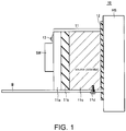
- FIG. 1 is a side view schematically illustrating an example of the exterior of the power conversion device according to embodiments of the present disclosure.
- FIG. 2 is a perspective view schematically illustrating an example of the exterior of the power conversion device according to embodiments of the present disclosure.
- the power conversion device illustrated in FIG. 1 is different in scale from the actual scale thereof in the thickness direction of a metal board 11 in order to explain the configuration.
- a power conversion device 10 is a device such as an inverter, a DC-DC converter or the like which performs control related to conversion of an output voltage and/or an output current using a semiconductor element SW which is a switching element.
- the semiconductor element SW is configured of a switching element such as a metal-oxide-semiconductor field-effect transistor (MOSFET), an insulated gate bipolar transistor (IGBT), or the like.
- the semiconductor element SW has a source terminal Ssw, a gate terminal Gsw and a drain terminal Dsw and is mounted on an external circuit of the metal board 11.
- One side of the metal board 11 is an external circuit 11a (circuit part) and the other side is a base metal 11c (metal part).
- the metal board 11 has an insulating layer 11b (insulating part) between the external circuit 11 a and the base metal 11c.
- the external circuit 11 a includes a wiring pattern for mounting the semiconductor element SW and has a thickness of about 18 to 300 ⁇ m.
- the base metal 11c is a metal plate formed of aluminum or copper and has a thickness of 0.5 to 30 mm.
- the base metal 11c is electrically connected to the source terminal Ssw of the semiconductor element SW through the wiring pattern formed on the external circuit 11a, which is not shown. That is, the potential of the base metal 11c is a stable potential (source potential).
- the base metal 11c has a screw tap formed thereon and the semiconductor element SW mounted on the external circuit 11a can be fixed using a screw 13.
- the metal board 11 is fixed onto a board B (circuit board).
- the board B comes into contact with a side surface of the metal board 11 and is fixed to the base metal 11c using a screw 11d (fixing member).
- the base metal 11c has a screw tap corresponding to the screw 11d.
- a heat sink (radiator) HS having a function of performing cooling by radiating heat generated from the semiconductor element SW to the outside is mounted on the board B approximately perpendicularly to the upper surface of the board B.
- the heat sink HS is a part of the power conversion device 10 and is electrically connected to a frame ground (FG) which will be described below.
- the heat sink HS is arranged at the side of the base metal 11c of the metal board 11 with an insulator 12 interposed therebetween. Accordingly, the semiconductor element SW radiates generated heat to the metal board 11 and the metal board 11 radiates the heat to the heat sink HS through the insulator 12.
- the base metal 11c of the metal board 11 is connected to the stable potential of the semiconductor element SW in order to reduce noise current flowing from a parasitic capacitance generated between the semiconductor element SW and the heat sink HS to the input side of the power conversion device 10.
- the semiconductor element SW has a heat-radiating surface attached to one side of the metal board 11 and the heat sink HS has a heat-absorbing surface attached to the other side of the metal board 11.
- FIG. 3 is a block diagram for describing a power supply apparatus 100 including the power conversion device 10 according to embodiments of the present disclosure.
- the power supply apparatus 100 including the power conversion device 10 includes a filter 20, an AC-DC converter 30 (AC/DC), the power conversion device 10 (DC/DC), and an insulating DC-DC converter 40 (insulating DC/DC).
- an AC power supply which is a commercial power supply 200 is connected to the filter which is an input side of the power supply apparatus 100 and a power load 300 (load) is connected to the insulating DC-DC converter which is an output side of the power supply apparatus 100.
- circuits from the AC power supply which is the commercial power supply 200 to the insulating DC-DC converter 40 are arranged in series on wires connected to live L, neutral N and ground FG.
- FIG. 4 is a circuit diagram of the power conversion device according to embodiments of the present disclosure.
- the filter 20 connected to the AC power supply (not shown)
- the AC-DC converter 30 such as a diode bridge which converts an AC supplied from the AC power supply to a DC
- the power conversion device 10 which performs power conversion such as voltage smoothing and boosting
- the insulating DC-DC converter 40 such as a transformer which performs conversion to a voltage and a current of standards depending on the power load 300 (not shown) are used.
- a DC converted from an AC by the AC-DC converter 30 is a pulsating current obtained when the direction of a minus voltage is inverted for an AC output from the filter 20 and has a fixed direction but a varying magnitude.
- a DC voltage supplied as a pulsating current is smoothed by the power conversion device 10.
- the power conversion device 10 includes a first line 12a and a second line 12b which connect the input side connected to the AC-DC converter 30 and the output side connected to the insulating DC-DC converter 40.
- the first line 12a and the second line 12b are connected to a first potential and a second potential of the input side.
- the first line 12a is connected to a plus side, for example, as the first potential.
- the second line 12b is connected to a minus side, for example, as the second potential and used as a wire connected to a stable potential lower than the first potential.
- a first capacitor C1 which connects the first line 12a and the second line 12b and performs smoothing is arranged at the input side which receives an input from the AC-DC converter 30.
- a boosting circuit (boosting chopper) using a reactor L1, the semiconductor element SW, a rectifying element D and a second capacitor C2 is arranged at the output side which performs output to the insulating DC-DC converter 40.
- the reactor L1 and the rectifying element D provided as the boosting circuit are connected in series on the first line 12a.
- the rectifying element D is arranged in such a manner that an anode terminal corresponds to the input side and a cathode terminal corresponds to the output side, and the reactor L1 is serially connected to the anode side.
- the second capacitor C2 is arranged at the side of the cathode of the rectifying element D to connect the first line 12a and the second line 12b.
- the semiconductor element SW of the boosting circuit is arranged such that the first line 12a and the second line 12b short-circuit.
- a MOSFET including an antiparallel diode is used as the semiconductor element SW.
- the drain terminal of the semiconductor element SW is connected to a first point P1 of the first line 12a between the reactor L1 and the rectifying element D, and the source terminal is connected to a second point P2 of the second line 12b.
- the second point P2 is positioned between a connection point at which the first capacitor C1 is connected to the second line 12b and a connection point at which the second capacitor C2 is connected to the second line 12b.
- the heat sink HS arranged in proximity to the right side of the semiconductor element SW is shown, and the metal board 11 is arranged between the semiconductor element SW and the heat sink HS.
- the heat sink HS is connected to a frame ground (FG) corresponding to a ground potential.
- the base metal 11c of the metal board 11 is connected to the second line 12b through a connection line 11e.
- a first parasitic capacitance Chp1 is generated between the semiconductor element SW and the heat sink HS.
- a second parasitic capacitance Chp2 is generated between the base metal 11c of the metal board 11 and the heat sink HS.
- a voltage variation at the first point P1 is transferred from the base metal 11c to the second line 12b through the second point P2 and thus a noise current Ins flows.
- the noise current Ins transferred to the second line 12b flows and circulates through the second point P2, the first capacitor C1, the reactor L1 and the first point P1 and is confined within the circuit composed of such elements and thus is not output as a noise to the input side of the power conversion device 10.
- the common mode current Icm can be represented by a value obtained by multiplying the second parasitic capacitance Chp2 by a temporal change of a voltage V2 of the second point P2.
- the voltage V2 of the second point P2 is the potential of the source terminal Ssw of the semiconductor element SW, which is a stable potential, and thus is less than a temporal change of a voltage V1 of the first point P1.
- the noise of the common mode current Icm caused by the temporal change at the second point P2 is less than the noise of the common mode current Icm caused by the temporal change at the first point P1, and thus the common mode current is so small that it can be ignored even when output to the input side of the power conversion device 10 as noise.
- the power conversion device 10 includes the metal board 11 of which one side is the external circuit 11a and the other side is the base metal 11c, the semiconductor element SW mounted on the external circuit 11a of the metal board 11, the insulator 12 arranged on the base metal 11c of the metal board 11, and the heat sink HS arranged at the base metal 11c of the metal board 11 having the insulating 12 interposed therebetween.
- the base metal 11c of the metal board 11 is connected to the stable potential of the semiconductor element SW. Accordingly, the noise current Ins caused by the first parasitic capacitance Chp1 generated between the base metal 11c of the metal board 11 and the semiconductor element SW can be confined within the power conversion device 10.
- the base metal 11c is connected to the second line 12b corresponding to the stable potential, and thus the common mode current Icm caused by the second parasitic capacitance Chp2 generated between the base metal 11c of the metal board 11 and the heat sink HS can be suppressed.
- the power conversion device 10 can be configured in such a manner that the semiconductor element SW, the metal board 11, the insulator 12 and the heat sink HS are stacked and thus can be reduced in size.
- the semiconductor element SW is fixed by forming a screw tap at the base metal 11c and using a screw, it is possible to reduce unnecessary structural components.
- the configuration of a conventional circuit board can be used for the board B by connecting the metal board 11 and the board B, and thus a board design can be simplified and manufacturing costs can be reduced.
- the metal board 11 has the insulating layer 11b between the external circuit 11 a and the base metal 11c, and the base metal 11c is connected to the stable potential of the semiconductor element SW through a wiring pattern formed on the external circuit 11a. Accordingly, it is possible to set the potential of the base metal 11c to the stable potential of the semiconductor element SW while securing insulation between the external circuit 11a and the base metal 11c.
- the board B comes into contact with a side surface of the metal board 11 and is fixed to the base metal 11c using the screw 11d (fixing member). Accordingly, it is possible to fix the metal board 11 on which the semiconductor element SW is mounted to the board B with stability.
- the power supply apparatus 100 including the power conversion device 10 according to embodiments of the present disclosure can decrease noise and can be reduced in size.
- the power conversion device 10 is not limited to the aforementioned embodiments and can be applied to various devices such as a DC-AC inverter and a DC chopper using a semiconductor switch in technical fields such as power electronics.
Landscapes
- Engineering & Computer Science (AREA)
- Power Engineering (AREA)
- Dc-Dc Converters (AREA)
- Inverter Devices (AREA)
Abstract
Description
- The present disclosure relates to a power conversion device and a power supply apparatus including a radiator for radiating heat generated from a semiconductor element.
- Power conversion devices for controlling an output voltage and the like by switching a semiconductor element which is a switching element are used for various purposes. A power conversion device is equipped with a radiator (heat sink) in order to radiate heat generated from a semiconductor element. For example, a power conversion device disclosed in Patent Document 1 includes a semiconductor element, a printed board on which the semiconductor element is mounted, and a radiator for radiating heat generated from the semiconductor element. In addition, the printed board includes a first printed pattern connected to a terminal having a potential that does not change in a switching operation of the semiconductor element and a second printed pattern connected to a terminal provided at the backside of the printed board and having a potential that changes in a switching operation of the semiconductor element.
- [Patent Document 1] Japanese Unexamined Patent Application Publication No.
2012-110231 - However, in a power conversion device, a parasitic capacitance generated between a radiator for radiating heat generated from a semiconductor element and the semiconductor element is large and thus noise caused by the parasitic capacitance is generated and output to an input side of the power conversion device. That is, the power conversion device has a problem that noise is generated due to coupling of a drain terminal of the semiconductor element and the radiator.
- In addition, in the power conversion device disclosed in Patent Document 1, a conductor used as a radiator is mounted on the printed board in addition to the first printed pattern and the second printed pattern. Accordingly, it is difficult to reduce the size of the power conversion device disclosed in Patent Document 1.
- The present disclosure is directed to provide a power conversion device and a power supply apparatus which can decrease noise and can be reduced in size.
- According to an embodiment of the present disclosure, a power conversion device includes: a metal board of which one side is a circuit part and the other side is a metal part; a semiconductor element mounted on the circuit part of the metal board; an insulator arranged on the metal part of the metal board; and a radiator arranged at the metal part of the metal board with the insulator interposed therebetween, wherein the metal part of the metal board is connected to a stable potential of the semiconductor element.
- Preferably, the metal board may have an insulating part between the circuit part and the metal part, and the stable potential of the semiconductor element and the metal part may be connected through a wiring pattern formed on the circuit part.
- Preferably, the semiconductor element may be fixed to the metal board through screwing. Preferably, the power conversion device may further include a circuit board connected to the metal board.
- Preferably, the circuit board may come into contact with a side surface of the metal board and may be fixed to the metal part using a fixing member.
- According to another embodiment of the present disclosure, a power supply apparatus includes the aforementioned power conversion device.
- According to the power conversion device according to the present technology, a semiconductor element is mounted on a circuit part of a metal board, a radiator is arranged at a metal part of the metal board having an insulator interposed therebetween, and the metal part of the metal board is connected to a stable potential of the semiconductor element, and thus a noise can be decreased and the size of the power conversion device can be reduced.
-
-
FIG. 1 is a side view schematically illustrating an example of the exterior of a power conversion device according to embodiments of the present disclosure. -
FIG. 2 is a perspective view schematically illustrating an example of the exterior of the power conversion device according to embodiments of the present disclosure. -
FIG. 3 is a block diagram for describing a power supply apparatus including the power conversion device according to embodiments of the present disclosure. -
FIG. 4 is a circuit diagram of the power conversion device according to embodiments of the present disclosure. - Hereinafter, the present embodiment will be described in detail with reference to the attached drawings. Meanwhile, the same reference numerals in the drawings represent the same or similar parts.
- The exterior of a power conversion device according to embodiments of the present disclosure will be described using the drawings.
FIG. 1 is a side view schematically illustrating an example of the exterior of the power conversion device according to embodiments of the present disclosure.FIG. 2 is a perspective view schematically illustrating an example of the exterior of the power conversion device according to embodiments of the present disclosure. Meanwhile, the power conversion device illustrated inFIG. 1 is different in scale from the actual scale thereof in the thickness direction of ametal board 11 in order to explain the configuration. - A
power conversion device 10 according to embodiments of the present disclosure is a device such as an inverter, a DC-DC converter or the like which performs control related to conversion of an output voltage and/or an output current using a semiconductor element SW which is a switching element. - The semiconductor element SW is configured of a switching element such as a metal-oxide-semiconductor field-effect transistor (MOSFET), an insulated gate bipolar transistor (IGBT), or the like. The semiconductor element SW has a source terminal Ssw, a gate terminal Gsw and a drain terminal Dsw and is mounted on an external circuit of the
metal board 11. One side of themetal board 11 is anexternal circuit 11a (circuit part) and the other side is abase metal 11c (metal part). Themetal board 11 has aninsulating layer 11b (insulating part) between theexternal circuit 11 a and thebase metal 11c. Theexternal circuit 11 a includes a wiring pattern for mounting the semiconductor element SW and has a thickness of about 18 to 300 µm. - The
base metal 11c is a metal plate formed of aluminum or copper and has a thickness of 0.5 to 30 mm. In addition, thebase metal 11c is electrically connected to the source terminal Ssw of the semiconductor element SW through the wiring pattern formed on theexternal circuit 11a, which is not shown. That is, the potential of thebase metal 11c is a stable potential (source potential). Thebase metal 11c has a screw tap formed thereon and the semiconductor element SW mounted on theexternal circuit 11a can be fixed using ascrew 13. - In addition, the
metal board 11 is fixed onto a board B (circuit board). The board B comes into contact with a side surface of themetal board 11 and is fixed to thebase metal 11c using ascrew 11d (fixing member). Thebase metal 11c has a screw tap corresponding to thescrew 11d. Further, a heat sink (radiator) HS having a function of performing cooling by radiating heat generated from the semiconductor element SW to the outside is mounted on the board B approximately perpendicularly to the upper surface of the board B. The heat sink HS is a part of thepower conversion device 10 and is electrically connected to a frame ground (FG) which will be described below. - The heat sink HS is arranged at the side of the
base metal 11c of themetal board 11 with aninsulator 12 interposed therebetween. Accordingly, the semiconductor element SW radiates generated heat to themetal board 11 and themetal board 11 radiates the heat to the heat sink HS through theinsulator 12. Thebase metal 11c of themetal board 11 is connected to the stable potential of the semiconductor element SW in order to reduce noise current flowing from a parasitic capacitance generated between the semiconductor element SW and the heat sink HS to the input side of thepower conversion device 10. - Meanwhile, to improve the efficiency of heat conduction of transferring the heat generated in the semiconductor element SW to the heat sink HS through the
metal board 11, the semiconductor element SW has a heat-radiating surface attached to one side of themetal board 11 and the heat sink HS has a heat-absorbing surface attached to the other side of themetal board 11. - Next, a circuit configuration of the
power conversion device 10 according to embodiments of the present disclosure will be described. For example, thepower conversion device 10 is used for a power supply apparatus.FIG. 3 is a block diagram for describing apower supply apparatus 100 including thepower conversion device 10 according to embodiments of the present disclosure. Thepower supply apparatus 100 including thepower conversion device 10 includes afilter 20, an AC-DC converter 30 (AC/DC), the power conversion device 10 (DC/DC), and an insulating DC-DC converter 40 (insulating DC/DC). In addition, an AC power supply which is acommercial power supply 200 is connected to the filter which is an input side of thepower supply apparatus 100 and a power load 300 (load) is connected to the insulating DC-DC converter which is an output side of thepower supply apparatus 100. Furthermore, circuits from the AC power supply which is thecommercial power supply 200 to the insulating DC-DC converter 40 are arranged in series on wires connected to live L, neutral N and ground FG. - The circuit configuration of the
power conversion device 10 will be described in more detail.FIG. 4 is a circuit diagram of the power conversion device according to embodiments of the present disclosure. In a control system illustrated inFIG. 4 , thefilter 20 connected to the AC power supply (not shown), the AC-DC converter 30 such as a diode bridge which converts an AC supplied from the AC power supply to a DC, thepower conversion device 10 which performs power conversion such as voltage smoothing and boosting, and the insulating DC-DC converter 40 such as a transformer which performs conversion to a voltage and a current of standards depending on the power load 300 (not shown) are used. A DC converted from an AC by the AC-DC converter 30 is a pulsating current obtained when the direction of a minus voltage is inverted for an AC output from thefilter 20 and has a fixed direction but a varying magnitude. In addition, a DC voltage supplied as a pulsating current is smoothed by thepower conversion device 10. - The
power conversion device 10 includes afirst line 12a and asecond line 12b which connect the input side connected to the AC-DC converter 30 and the output side connected to the insulating DC-DC converter 40. Thefirst line 12a and thesecond line 12b are connected to a first potential and a second potential of the input side. Thefirst line 12a is connected to a plus side, for example, as the first potential. Thesecond line 12b is connected to a minus side, for example, as the second potential and used as a wire connected to a stable potential lower than the first potential. - In the
power conversion device 10, a first capacitor C1 which connects thefirst line 12a and thesecond line 12b and performs smoothing is arranged at the input side which receives an input from the AC-DC converter 30. In addition, a boosting circuit (boosting chopper) using a reactor L1, the semiconductor element SW, a rectifying element D and a second capacitor C2 is arranged at the output side which performs output to the insulating DC-DC converter 40. - The reactor L1 and the rectifying element D provided as the boosting circuit are connected in series on the
first line 12a. The rectifying element D is arranged in such a manner that an anode terminal corresponds to the input side and a cathode terminal corresponds to the output side, and the reactor L1 is serially connected to the anode side. In addition, the second capacitor C2 is arranged at the side of the cathode of the rectifying element D to connect thefirst line 12a and thesecond line 12b. - Further, the semiconductor element SW of the boosting circuit is arranged such that the
first line 12a and thesecond line 12b short-circuit. In the circuit illustrated inFIG. 4 , a MOSFET including an antiparallel diode is used as the semiconductor element SW. The drain terminal of the semiconductor element SW is connected to a first point P1 of thefirst line 12a between the reactor L1 and the rectifying element D, and the source terminal is connected to a second point P2 of thesecond line 12b. Further, the second point P2 is positioned between a connection point at which the first capacitor C1 is connected to thesecond line 12b and a connection point at which the second capacitor C2 is connected to thesecond line 12b. - In
FIG. 4 , the heat sink HS arranged in proximity to the right side of the semiconductor element SW is shown, and themetal board 11 is arranged between the semiconductor element SW and the heat sink HS. The heat sink HS is connected to a frame ground (FG) corresponding to a ground potential. Thebase metal 11c of themetal board 11 is connected to thesecond line 12b through aconnection line 11e. - When the heat sink HS is connected to the FG, a first parasitic capacitance Chp1 is generated between the semiconductor element SW and the heat sink HS. In addition, a second parasitic capacitance Chp2 is generated between the
base metal 11c of themetal board 11 and the heat sink HS. - Due to the first parasitic capacitance Chp1 generated between the
base metal 11c of themetal board 11 and the semiconductor element SW, a voltage variation at the first point P1 is transferred from thebase metal 11c to thesecond line 12b through the second point P2 and thus a noise current Ins flows. However, the noise current Ins transferred to thesecond line 12b flows and circulates through the second point P2, the first capacitor C1, the reactor L1 and the first point P1 and is confined within the circuit composed of such elements and thus is not output as a noise to the input side of thepower conversion device 10. - In addition, due to the second parasitic capacitance Chp2 generated between the
base metal 11c of themetal board 11 and the heat sink HS, a voltage variation at the second point P2 is transferred from the heat sink HS to the FG and thus a common mode current Icm flows as noise. The common mode current Icm can be represented by a value obtained by multiplying the second parasitic capacitance Chp2 by a temporal change of a voltage V2 of the second point P2. In addition, the voltage V2 of the second point P2 is the potential of the source terminal Ssw of the semiconductor element SW, which is a stable potential, and thus is less than a temporal change of a voltage V1 of the first point P1. Accordingly, the noise of the common mode current Icm caused by the temporal change at the second point P2 is less than the noise of the common mode current Icm caused by the temporal change at the first point P1, and thus the common mode current is so small that it can be ignored even when output to the input side of thepower conversion device 10 as noise. - As described above, the
power conversion device 10 according to embodiments of the present disclosure includes themetal board 11 of which one side is theexternal circuit 11a and the other side is thebase metal 11c, the semiconductor element SW mounted on theexternal circuit 11a of themetal board 11, theinsulator 12 arranged on thebase metal 11c of themetal board 11, and the heat sink HS arranged at thebase metal 11c of themetal board 11 having the insulating 12 interposed therebetween. In addition, thebase metal 11c of themetal board 11 is connected to the stable potential of the semiconductor element SW. Accordingly, the noise current Ins caused by the first parasitic capacitance Chp1 generated between thebase metal 11c of themetal board 11 and the semiconductor element SW can be confined within thepower conversion device 10. Furthermore, thebase metal 11c is connected to thesecond line 12b corresponding to the stable potential, and thus the common mode current Icm caused by the second parasitic capacitance Chp2 generated between thebase metal 11c of themetal board 11 and the heat sink HS can be suppressed. Moreover, thepower conversion device 10 can be configured in such a manner that the semiconductor element SW, themetal board 11, theinsulator 12 and the heat sink HS are stacked and thus can be reduced in size. - Further, since the semiconductor element SW is fixed by forming a screw tap at the
base metal 11c and using a screw, it is possible to reduce unnecessary structural components. - In addition, the configuration of a conventional circuit board can be used for the board B by connecting the
metal board 11 and the board B, and thus a board design can be simplified and manufacturing costs can be reduced. - Moreover, the
metal board 11 has the insulatinglayer 11b between theexternal circuit 11 a and thebase metal 11c, and thebase metal 11c is connected to the stable potential of the semiconductor element SW through a wiring pattern formed on theexternal circuit 11a. Accordingly, it is possible to set the potential of thebase metal 11c to the stable potential of the semiconductor element SW while securing insulation between theexternal circuit 11a and thebase metal 11c. - Furthermore, the board B comes into contact with a side surface of the
metal board 11 and is fixed to thebase metal 11c using thescrew 11d (fixing member). Accordingly, it is possible to fix themetal board 11 on which the semiconductor element SW is mounted to the board B with stability. - Further, the
power supply apparatus 100 including thepower conversion device 10 according to embodiments of the present disclosure can decrease noise and can be reduced in size. - In addition, the
power conversion device 10 according to embodiments of the present disclosure is not limited to the aforementioned embodiments and can be applied to various devices such as a DC-AC inverter and a DC chopper using a semiconductor switch in technical fields such as power electronics. -
- 10: power conversion device
- 11: metal board
- 11a: external circuit
- 11b: insulating layer
- 11c: base metal
- 12a: first line
- 12b: second line
- HS: heat sink
- SW: semiconductor element
Claims (6)
- A power conversion device (10), comprising:a metal board (11) of which one side is a circuit part and the other side is a metal part;a semiconductor element (SW) mounted on the circuit part of the metal board (11);an insulator (12) arranged on the metal part of the metal board (11); anda radiator arranged at the metal part of the metal board (11) having the insulator (12) interposed between the radiator and the metal part,wherein the metal part of the metal board (11) is connected to a stable potential of the semiconductor element (SW).
- The power conversion device (10) according to claim 1, wherein the metal board (11) has an insulating part between the circuit part and the metal part, and the stable potential of the semiconductor element (SW) and the metal part are connected through a wiring pattern formed on the circuit part.
- The power conversion device (10) according to claim 1 or 2, wherein the semiconductor element (SW) is fixed to the metal board (11) through screwing.
- The power conversion device (10) according to any one of claims 1 to 3, further comprising:a circuit board connected to the metal board (11).
- The power conversion device (10) according to claim 4, wherein the circuit board comes into contact with a side surface of the metal board (11) and is fixed to the metal part using a fixing member.
- A power supply apparatus (100), comprising the power conversion device (10) according to any one of claims 1 to 5.
Applications Claiming Priority (1)
| Application Number | Priority Date | Filing Date | Title |
|---|---|---|---|
| JP2017047399A JP6880851B2 (en) | 2017-03-13 | 2017-03-13 | Power converter and power supply |
Publications (2)
| Publication Number | Publication Date |
|---|---|
| EP3376658A1 true EP3376658A1 (en) | 2018-09-19 |
| EP3376658B1 EP3376658B1 (en) | 2020-12-02 |
Family
ID=60935642
Family Applications (1)
| Application Number | Title | Priority Date | Filing Date |
|---|---|---|---|
| EP17207714.1A Active EP3376658B1 (en) | 2017-03-13 | 2017-12-15 | Power conversion device and power supply apparatus |
Country Status (3)
| Country | Link |
|---|---|
| EP (1) | EP3376658B1 (en) |
| JP (1) | JP6880851B2 (en) |
| CN (1) | CN108573941A (en) |
Families Citing this family (1)
| Publication number | Priority date | Publication date | Assignee | Title |
|---|---|---|---|---|
| JPWO2024203125A1 (en) * | 2023-03-27 | 2024-10-03 |
Citations (4)
| Publication number | Priority date | Publication date | Assignee | Title |
|---|---|---|---|---|
| JP2012110231A (en) | 2012-03-15 | 2012-06-07 | Fuji Electric Co Ltd | Power conversion device |
| WO2016017260A1 (en) * | 2014-07-30 | 2016-02-04 | 富士電機株式会社 | Semiconductor module |
| WO2016194050A1 (en) * | 2015-05-29 | 2016-12-08 | 日産自動車株式会社 | Power conversion device |
| WO2017002398A1 (en) * | 2015-06-30 | 2017-01-05 | オムロン株式会社 | Power conversion device |
Family Cites Families (7)
| Publication number | Priority date | Publication date | Assignee | Title |
|---|---|---|---|---|
| JPH11513841A (en) * | 1995-10-13 | 1999-11-24 | サーマロイ,インコーポレイテッド | Solderable transistor clips and heat sinks |
| JP3239082B2 (en) * | 1997-04-23 | 2001-12-17 | 三洋電機株式会社 | Hybrid integrated circuit device |
| JPH11266090A (en) * | 1998-03-17 | 1999-09-28 | Denso Corp | Semiconductor device |
| JP3858834B2 (en) * | 2003-02-24 | 2006-12-20 | オンキヨー株式会社 | Semiconductor element heatsink |
| JP2008136333A (en) * | 2006-10-30 | 2008-06-12 | Denso Corp | Power converter |
| US9099906B2 (en) * | 2010-07-06 | 2015-08-04 | Mitsubishi Electric Corporation | Inverter |
| WO2013080441A1 (en) * | 2011-11-30 | 2013-06-06 | 富士電機株式会社 | Power conversion device |
-
2017
- 2017-03-13 JP JP2017047399A patent/JP6880851B2/en active Active
- 2017-12-15 EP EP17207714.1A patent/EP3376658B1/en active Active
- 2017-12-15 CN CN201711360187.6A patent/CN108573941A/en active Pending
Patent Citations (4)
| Publication number | Priority date | Publication date | Assignee | Title |
|---|---|---|---|---|
| JP2012110231A (en) | 2012-03-15 | 2012-06-07 | Fuji Electric Co Ltd | Power conversion device |
| WO2016017260A1 (en) * | 2014-07-30 | 2016-02-04 | 富士電機株式会社 | Semiconductor module |
| WO2016194050A1 (en) * | 2015-05-29 | 2016-12-08 | 日産自動車株式会社 | Power conversion device |
| WO2017002398A1 (en) * | 2015-06-30 | 2017-01-05 | オムロン株式会社 | Power conversion device |
Also Published As
| Publication number | Publication date |
|---|---|
| CN108573941A (en) | 2018-09-25 |
| JP2018152993A (en) | 2018-09-27 |
| EP3376658B1 (en) | 2020-12-02 |
| JP6880851B2 (en) | 2021-06-02 |
Similar Documents
| Publication | Publication Date | Title |
|---|---|---|
| US7542316B2 (en) | Switching power supply unit | |
| US9653386B2 (en) | Compact multi-die power semiconductor package | |
| US20160315038A1 (en) | Semiconductor module | |
| JP6158051B2 (en) | Power converter | |
| US10361628B2 (en) | Power converter | |
| US10244617B2 (en) | Power converter | |
| JP2000091884A (en) | Electronic circuit device | |
| US11404970B2 (en) | Power converter | |
| CN104518681B (en) | Power-converting device | |
| JP2019201187A (en) | Electronic circuit device | |
| EP3376658B1 (en) | Power conversion device and power supply apparatus | |
| JP2018143010A (en) | Electronic circuit device | |
| JP5675526B2 (en) | Power converter | |
| JP2006288052A (en) | Dc-dc converter | |
| JP2010088153A (en) | Electronic equipment | |
| US20250081414A1 (en) | Rectifying-element-module cooling unit | |
| TWI789400B (en) | Charger | |
| JP2002232170A (en) | Connection structure between printed circuit board and heat sink | |
| JP2025023448A (en) | Power Supplies | |
| US9704787B2 (en) | Compact single-die power semiconductor package | |
| WO2024254248A1 (en) | Package for power module | |
| JP2021182828A (en) | Power converter | |
| JP2002016207A (en) | Semiconductor block and power supply device using the same |
Legal Events
| Date | Code | Title | Description |
|---|---|---|---|
| PUAI | Public reference made under article 153(3) epc to a published international application that has entered the european phase |
Free format text: ORIGINAL CODE: 0009012 |
|
| STAA | Information on the status of an ep patent application or granted ep patent |
Free format text: STATUS: REQUEST FOR EXAMINATION WAS MADE |
|
| 17P | Request for examination filed |
Effective date: 20171215 |
|
| AK | Designated contracting states |
Kind code of ref document: A1 Designated state(s): AL AT BE BG CH CY CZ DE DK EE ES FI FR GB GR HR HU IE IS IT LI LT LU LV MC MK MT NL NO PL PT RO RS SE SI SK SM TR |
|
| AX | Request for extension of the european patent |
Extension state: BA ME |
|
| RBV | Designated contracting states (corrected) |
Designated state(s): AL AT BE BG CH CY CZ DE DK EE ES FI FR GB GR HR HU IE IS IT LI LT LU LV MC MK MT NL NO PL PT RO RS SE SI SK SM TR |
|
| GRAP | Despatch of communication of intention to grant a patent |
Free format text: ORIGINAL CODE: EPIDOSNIGR1 |
|
| STAA | Information on the status of an ep patent application or granted ep patent |
Free format text: STATUS: GRANT OF PATENT IS INTENDED |
|
| INTG | Intention to grant announced |
Effective date: 20200707 |
|
| GRAS | Grant fee paid |
Free format text: ORIGINAL CODE: EPIDOSNIGR3 |
|
| GRAA | (expected) grant |
Free format text: ORIGINAL CODE: 0009210 |
|
| STAA | Information on the status of an ep patent application or granted ep patent |
Free format text: STATUS: THE PATENT HAS BEEN GRANTED |
|
| AK | Designated contracting states |
Kind code of ref document: B1 Designated state(s): AL AT BE BG CH CY CZ DE DK EE ES FI FR GB GR HR HU IE IS IT LI LT LU LV MC MK MT NL NO PL PT RO RS SE SI SK SM TR |
|
| REG | Reference to a national code |
Ref country code: GB Ref legal event code: FG4D |
|
| REG | Reference to a national code |
Ref country code: AT Ref legal event code: REF Ref document number: 1342012 Country of ref document: AT Kind code of ref document: T Effective date: 20201215 Ref country code: CH Ref legal event code: EP |
|
| REG | Reference to a national code |
Ref country code: DE Ref legal event code: R096 Ref document number: 602017028702 Country of ref document: DE |
|
| REG | Reference to a national code |
Ref country code: IE Ref legal event code: FG4D |
|
| PG25 | Lapsed in a contracting state [announced via postgrant information from national office to epo] |
Ref country code: GR Free format text: LAPSE BECAUSE OF FAILURE TO SUBMIT A TRANSLATION OF THE DESCRIPTION OR TO PAY THE FEE WITHIN THE PRESCRIBED TIME-LIMIT Effective date: 20210303 Ref country code: FI Free format text: LAPSE BECAUSE OF FAILURE TO SUBMIT A TRANSLATION OF THE DESCRIPTION OR TO PAY THE FEE WITHIN THE PRESCRIBED TIME-LIMIT Effective date: 20201202 Ref country code: NO Free format text: LAPSE BECAUSE OF FAILURE TO SUBMIT A TRANSLATION OF THE DESCRIPTION OR TO PAY THE FEE WITHIN THE PRESCRIBED TIME-LIMIT Effective date: 20210302 Ref country code: RS Free format text: LAPSE BECAUSE OF FAILURE TO SUBMIT A TRANSLATION OF THE DESCRIPTION OR TO PAY THE FEE WITHIN THE PRESCRIBED TIME-LIMIT Effective date: 20201202 |
|
| REG | Reference to a national code |
Ref country code: NL Ref legal event code: MP Effective date: 20201202 |
|
| REG | Reference to a national code |
Ref country code: AT Ref legal event code: MK05 Ref document number: 1342012 Country of ref document: AT Kind code of ref document: T Effective date: 20201202 |
|
| PG25 | Lapsed in a contracting state [announced via postgrant information from national office to epo] |
Ref country code: SE Free format text: LAPSE BECAUSE OF FAILURE TO SUBMIT A TRANSLATION OF THE DESCRIPTION OR TO PAY THE FEE WITHIN THE PRESCRIBED TIME-LIMIT Effective date: 20201202 Ref country code: BG Free format text: LAPSE BECAUSE OF FAILURE TO SUBMIT A TRANSLATION OF THE DESCRIPTION OR TO PAY THE FEE WITHIN THE PRESCRIBED TIME-LIMIT Effective date: 20210302 Ref country code: PL Free format text: LAPSE BECAUSE OF FAILURE TO SUBMIT A TRANSLATION OF THE DESCRIPTION OR TO PAY THE FEE WITHIN THE PRESCRIBED TIME-LIMIT Effective date: 20201202 Ref country code: LV Free format text: LAPSE BECAUSE OF FAILURE TO SUBMIT A TRANSLATION OF THE DESCRIPTION OR TO PAY THE FEE WITHIN THE PRESCRIBED TIME-LIMIT Effective date: 20201202 |
|
| PG25 | Lapsed in a contracting state [announced via postgrant information from national office to epo] |
Ref country code: NL Free format text: LAPSE BECAUSE OF FAILURE TO SUBMIT A TRANSLATION OF THE DESCRIPTION OR TO PAY THE FEE WITHIN THE PRESCRIBED TIME-LIMIT Effective date: 20201202 Ref country code: HR Free format text: LAPSE BECAUSE OF FAILURE TO SUBMIT A TRANSLATION OF THE DESCRIPTION OR TO PAY THE FEE WITHIN THE PRESCRIBED TIME-LIMIT Effective date: 20201202 |
|
| REG | Reference to a national code |
Ref country code: LT Ref legal event code: MG9D |
|
| PG25 | Lapsed in a contracting state [announced via postgrant information from national office to epo] |
Ref country code: LT Free format text: LAPSE BECAUSE OF FAILURE TO SUBMIT A TRANSLATION OF THE DESCRIPTION OR TO PAY THE FEE WITHIN THE PRESCRIBED TIME-LIMIT Effective date: 20201202 Ref country code: CZ Free format text: LAPSE BECAUSE OF FAILURE TO SUBMIT A TRANSLATION OF THE DESCRIPTION OR TO PAY THE FEE WITHIN THE PRESCRIBED TIME-LIMIT Effective date: 20201202 Ref country code: EE Free format text: LAPSE BECAUSE OF FAILURE TO SUBMIT A TRANSLATION OF THE DESCRIPTION OR TO PAY THE FEE WITHIN THE PRESCRIBED TIME-LIMIT Effective date: 20201202 Ref country code: SM Free format text: LAPSE BECAUSE OF FAILURE TO SUBMIT A TRANSLATION OF THE DESCRIPTION OR TO PAY THE FEE WITHIN THE PRESCRIBED TIME-LIMIT Effective date: 20201202 Ref country code: PT Free format text: LAPSE BECAUSE OF FAILURE TO SUBMIT A TRANSLATION OF THE DESCRIPTION OR TO PAY THE FEE WITHIN THE PRESCRIBED TIME-LIMIT Effective date: 20210405 Ref country code: SK Free format text: LAPSE BECAUSE OF FAILURE TO SUBMIT A TRANSLATION OF THE DESCRIPTION OR TO PAY THE FEE WITHIN THE PRESCRIBED TIME-LIMIT Effective date: 20201202 Ref country code: RO Free format text: LAPSE BECAUSE OF FAILURE TO SUBMIT A TRANSLATION OF THE DESCRIPTION OR TO PAY THE FEE WITHIN THE PRESCRIBED TIME-LIMIT Effective date: 20201202 |
|
| REG | Reference to a national code |
Ref country code: CH Ref legal event code: PL |
|
| PG25 | Lapsed in a contracting state [announced via postgrant information from national office to epo] |
Ref country code: AT Free format text: LAPSE BECAUSE OF FAILURE TO SUBMIT A TRANSLATION OF THE DESCRIPTION OR TO PAY THE FEE WITHIN THE PRESCRIBED TIME-LIMIT Effective date: 20201202 |
|
| REG | Reference to a national code |
Ref country code: DE Ref legal event code: R097 Ref document number: 602017028702 Country of ref document: DE Ref country code: BE Ref legal event code: MM Effective date: 20201231 |
|
| PG25 | Lapsed in a contracting state [announced via postgrant information from national office to epo] |
Ref country code: IS Free format text: LAPSE BECAUSE OF FAILURE TO SUBMIT A TRANSLATION OF THE DESCRIPTION OR TO PAY THE FEE WITHIN THE PRESCRIBED TIME-LIMIT Effective date: 20210402 Ref country code: MC Free format text: LAPSE BECAUSE OF FAILURE TO SUBMIT A TRANSLATION OF THE DESCRIPTION OR TO PAY THE FEE WITHIN THE PRESCRIBED TIME-LIMIT Effective date: 20201202 |
|
| PLBE | No opposition filed within time limit |
Free format text: ORIGINAL CODE: 0009261 |
|
| STAA | Information on the status of an ep patent application or granted ep patent |
Free format text: STATUS: NO OPPOSITION FILED WITHIN TIME LIMIT |
|
| PG25 | Lapsed in a contracting state [announced via postgrant information from national office to epo] |
Ref country code: FR Free format text: LAPSE BECAUSE OF NON-PAYMENT OF DUE FEES Effective date: 20210202 Ref country code: IE Free format text: LAPSE BECAUSE OF NON-PAYMENT OF DUE FEES Effective date: 20201215 Ref country code: AL Free format text: LAPSE BECAUSE OF FAILURE TO SUBMIT A TRANSLATION OF THE DESCRIPTION OR TO PAY THE FEE WITHIN THE PRESCRIBED TIME-LIMIT Effective date: 20201202 Ref country code: IT Free format text: LAPSE BECAUSE OF FAILURE TO SUBMIT A TRANSLATION OF THE DESCRIPTION OR TO PAY THE FEE WITHIN THE PRESCRIBED TIME-LIMIT Effective date: 20201202 Ref country code: LU Free format text: LAPSE BECAUSE OF NON-PAYMENT OF DUE FEES Effective date: 20201215 |
|
| 26N | No opposition filed |
Effective date: 20210903 |
|
| PG25 | Lapsed in a contracting state [announced via postgrant information from national office to epo] |
Ref country code: DK Free format text: LAPSE BECAUSE OF FAILURE TO SUBMIT A TRANSLATION OF THE DESCRIPTION OR TO PAY THE FEE WITHIN THE PRESCRIBED TIME-LIMIT Effective date: 20201202 Ref country code: CH Free format text: LAPSE BECAUSE OF NON-PAYMENT OF DUE FEES Effective date: 20201231 Ref country code: SI Free format text: LAPSE BECAUSE OF FAILURE TO SUBMIT A TRANSLATION OF THE DESCRIPTION OR TO PAY THE FEE WITHIN THE PRESCRIBED TIME-LIMIT Effective date: 20201202 Ref country code: LI Free format text: LAPSE BECAUSE OF NON-PAYMENT OF DUE FEES Effective date: 20201231 |
|
| PG25 | Lapsed in a contracting state [announced via postgrant information from national office to epo] |
Ref country code: ES Free format text: LAPSE BECAUSE OF FAILURE TO SUBMIT A TRANSLATION OF THE DESCRIPTION OR TO PAY THE FEE WITHIN THE PRESCRIBED TIME-LIMIT Effective date: 20201202 |
|
| PG25 | Lapsed in a contracting state [announced via postgrant information from national office to epo] |
Ref country code: IS Free format text: LAPSE BECAUSE OF FAILURE TO SUBMIT A TRANSLATION OF THE DESCRIPTION OR TO PAY THE FEE WITHIN THE PRESCRIBED TIME-LIMIT Effective date: 20210402 Ref country code: TR Free format text: LAPSE BECAUSE OF FAILURE TO SUBMIT A TRANSLATION OF THE DESCRIPTION OR TO PAY THE FEE WITHIN THE PRESCRIBED TIME-LIMIT Effective date: 20201202 Ref country code: MT Free format text: LAPSE BECAUSE OF FAILURE TO SUBMIT A TRANSLATION OF THE DESCRIPTION OR TO PAY THE FEE WITHIN THE PRESCRIBED TIME-LIMIT Effective date: 20201202 Ref country code: CY Free format text: LAPSE BECAUSE OF FAILURE TO SUBMIT A TRANSLATION OF THE DESCRIPTION OR TO PAY THE FEE WITHIN THE PRESCRIBED TIME-LIMIT Effective date: 20201202 |
|
| PG25 | Lapsed in a contracting state [announced via postgrant information from national office to epo] |
Ref country code: MK Free format text: LAPSE BECAUSE OF FAILURE TO SUBMIT A TRANSLATION OF THE DESCRIPTION OR TO PAY THE FEE WITHIN THE PRESCRIBED TIME-LIMIT Effective date: 20201202 |
|
| PG25 | Lapsed in a contracting state [announced via postgrant information from national office to epo] |
Ref country code: BE Free format text: LAPSE BECAUSE OF NON-PAYMENT OF DUE FEES Effective date: 20201231 |
|
| GBPC | Gb: european patent ceased through non-payment of renewal fee |
Effective date: 20211215 |
|
| PG25 | Lapsed in a contracting state [announced via postgrant information from national office to epo] |
Ref country code: GB Free format text: LAPSE BECAUSE OF NON-PAYMENT OF DUE FEES Effective date: 20211215 |
|
| PGFP | Annual fee paid to national office [announced via postgrant information from national office to epo] |
Ref country code: DE Payment date: 20251222 Year of fee payment: 9 |