EP3376544B1 - Optische bildanzeigevorrichtung - Google Patents
Optische bildanzeigevorrichtung Download PDFInfo
- Publication number
- EP3376544B1 EP3376544B1 EP18161920.6A EP18161920A EP3376544B1 EP 3376544 B1 EP3376544 B1 EP 3376544B1 EP 18161920 A EP18161920 A EP 18161920A EP 3376544 B1 EP3376544 B1 EP 3376544B1
- Authority
- EP
- European Patent Office
- Prior art keywords
- light sources
- photo
- image
- detectors
- imaging device
- Prior art date
- Legal status (The legal status is an assumption and is not a legal conclusion. Google has not performed a legal analysis and makes no representation as to the accuracy of the status listed.)
- Active
Links
Images


Classifications
-
- G—PHYSICS
- G06—COMPUTING OR CALCULATING; COUNTING
- G06V—IMAGE OR VIDEO RECOGNITION OR UNDERSTANDING
- G06V40/00—Recognition of biometric, human-related or animal-related patterns in image or video data
- G06V40/10—Human or animal bodies, e.g. vehicle occupants or pedestrians; Body parts, e.g. hands
- G06V40/12—Fingerprints or palmprints
- G06V40/13—Sensors therefor
- G06V40/1324—Sensors therefor by using geometrical optics, e.g. using prisms
-
- H—ELECTRICITY
- H10—SEMICONDUCTOR DEVICES; ELECTRIC SOLID-STATE DEVICES NOT OTHERWISE PROVIDED FOR
- H10F—INORGANIC SEMICONDUCTOR DEVICES SENSITIVE TO INFRARED RADIATION, LIGHT, ELECTROMAGNETIC RADIATION OF SHORTER WAVELENGTH OR CORPUSCULAR RADIATION
- H10F39/00—Integrated devices, or assemblies of multiple devices, comprising at least one element covered by group H10F30/00, e.g. radiation detectors comprising photodiode arrays
- H10F39/80—Constructional details of image sensors
- H10F39/803—Pixels having integrated switching, control, storage or amplification elements
-
- G—PHYSICS
- G06—COMPUTING OR CALCULATING; COUNTING
- G06V—IMAGE OR VIDEO RECOGNITION OR UNDERSTANDING
- G06V40/00—Recognition of biometric, human-related or animal-related patterns in image or video data
- G06V40/10—Human or animal bodies, e.g. vehicle occupants or pedestrians; Body parts, e.g. hands
- G06V40/12—Fingerprints or palmprints
- G06V40/13—Sensors therefor
- G06V40/1318—Sensors therefor using electro-optical elements or layers, e.g. electroluminescent sensing
-
- G—PHYSICS
- G06—COMPUTING OR CALCULATING; COUNTING
- G06V—IMAGE OR VIDEO RECOGNITION OR UNDERSTANDING
- G06V40/00—Recognition of biometric, human-related or animal-related patterns in image or video data
- G06V40/10—Human or animal bodies, e.g. vehicle occupants or pedestrians; Body parts, e.g. hands
- G06V40/12—Fingerprints or palmprints
- G06V40/1335—Combining adjacent partial images (e.g. slices) to create a composite input or reference pattern; Tracking a sweeping finger movement
-
- H—ELECTRICITY
- H05—ELECTRIC TECHNIQUES NOT OTHERWISE PROVIDED FOR
- H05B—ELECTRIC HEATING; ELECTRIC LIGHT SOURCES NOT OTHERWISE PROVIDED FOR; CIRCUIT ARRANGEMENTS FOR ELECTRIC LIGHT SOURCES, IN GENERAL
- H05B45/00—Circuit arrangements for operating light-emitting diodes [LED]
- H05B45/30—Driver circuits
-
- H—ELECTRICITY
- H10—SEMICONDUCTOR DEVICES; ELECTRIC SOLID-STATE DEVICES NOT OTHERWISE PROVIDED FOR
- H10F—INORGANIC SEMICONDUCTOR DEVICES SENSITIVE TO INFRARED RADIATION, LIGHT, ELECTROMAGNETIC RADIATION OF SHORTER WAVELENGTH OR CORPUSCULAR RADIATION
- H10F39/00—Integrated devices, or assemblies of multiple devices, comprising at least one element covered by group H10F30/00, e.g. radiation detectors comprising photodiode arrays
- H10F39/10—Integrated devices
- H10F39/12—Image sensors
- H10F39/18—Complementary metal-oxide-semiconductor [CMOS] image sensors; Photodiode array image sensors
-
- H—ELECTRICITY
- H10—SEMICONDUCTOR DEVICES; ELECTRIC SOLID-STATE DEVICES NOT OTHERWISE PROVIDED FOR
- H10F—INORGANIC SEMICONDUCTOR DEVICES SENSITIVE TO INFRARED RADIATION, LIGHT, ELECTROMAGNETIC RADIATION OF SHORTER WAVELENGTH OR CORPUSCULAR RADIATION
- H10F39/00—Integrated devices, or assemblies of multiple devices, comprising at least one element covered by group H10F30/00, e.g. radiation detectors comprising photodiode arrays
- H10F39/10—Integrated devices
- H10F39/12—Image sensors
- H10F39/198—Contact-type image sensors [CIS]
-
- H—ELECTRICITY
- H10—SEMICONDUCTOR DEVICES; ELECTRIC SOLID-STATE DEVICES NOT OTHERWISE PROVIDED FOR
- H10K—ORGANIC ELECTRIC SOLID-STATE DEVICES
- H10K59/00—Integrated devices, or assemblies of multiple devices, comprising at least one organic light-emitting element covered by group H10K50/00
- H10K59/60—OLEDs integrated with inorganic light-sensitive elements, e.g. with inorganic solar cells or inorganic photodiodes
- H10K59/65—OLEDs integrated with inorganic image sensors
Definitions
- the invention relates to the field of optical imaging devices, and in particular that of fingerprint sensors, configured to carry out image capture optically, that is to say by carrying out light detection.
- a fingerprint sensor performing optical image capture, it is known to use an OLED (organic light-emitting diode) type light source produced on a transparent substrate, and a photo-detector such as a diode. to read the signal.
- OLED organic light-emitting diode
- a photo-detector such as a diode.
- the photo-detector for example a PIN diode
- a light source for example an organic light-emitting diode
- the document US 2007/291325 A1 describes a device combining an imager function and a display function.
- the document US 5,627,364 A describes a linear imaging device comprising a substrate 30 on which several photodetector elements are formed and a light source formed linearly along the photodetector elements.
- the document US 2002/079512 A1 describes an imaging device combining a matrix of light sources forming a display screen and a matrix of photodetectors interleaved with the matrix of light sources.
- An aim of the present invention is to propose an imaging device configured to implement optical detection of an element to be imaged in a configuration which is not in the near field, that is to say which is compatible with the presence a thick protective element between the element to be imaged and the electronic elements of the imaging device (photo-detectors and light sources), which does not require the presence of optical guidance means between the element to be imaged and the photo- detectors of the imaging device.
- the pitch of the photodetectors corresponds to the distance separating the centers of the photosensitive portions of two neighboring photodetectors arranged on the same row or the same column of the photodetector matrix. This pitch is for example equal to approximately 50 ⁇ m. In this case, the optical medium may have a thickness greater than 50 ⁇ m.
- the step considered to define the minimum thickness of the medium optical is the one having the greatest value among the different steps present within the photo-detector matrix.
- the light sources emit rays of light substantially isotropically through the optical medium.
- the rays forming, with the capture surface, an angle of incidence between the first and second limiting angles of refraction as defined above part of these rays are reflected by the interface between the optical medium and the environment external to the device, that is to say at the level of the capture surface, when the external environment reached by these rays corresponds to the external environment, or the atmosphere (air), in which the element is located to be imaged, and other rays cross this interface when the external environment reached by these other rays corresponds to the element to be imaged (phenomenon of frustrated total reflection).
- the reflected light rays containing the information to be detected by the photodetectors correspond to those delimited by the first and second limit angles of refraction.
- partial images of the element to be imaged are obtained which are detected by the photo-detectors located in the region illuminated by these reflected rays.
- a desired final image of the element to be imaged can thus be constructed from these partial images.
- This imaging device judiciously uses a thick optical medium which serves both for the propagation of light rays from the light sources to the photo-detectors (via reflection on the capture surface), and for the protection of electronic elements (in particular light sources and photodetectors) of the imaging device.
- the optical medium can correspond to a glass plate of a display screen. At least part of the light sources of the pixels of this screen can form the light sources of the imaging device (all the light sources of the screen are not necessarily used to carry out the various image acquisitions).
- this imaging device it is not necessary to thin the glass plate at the location of the photodetector matrix. because the imaging device works perfectly with, as optical medium, a glass corresponding to a standard protective glass of a screen.
- the presence of this thick optical medium does not cause any loss of precision in the captured image because this optical medium is part of the imaging device and does not disrupt its operation.
- the resolution of the final image obtained of the element to be imaged is greater than the resolution with which the matrix of photo-detectors is produced due to the fact that optical magnification is naturally obtained given the path of the light rays at the within the optical medium (with a reflection against the capture surface), and this without having dedicated magnification optics present in the imaging device.
- an optical magnification equal to 2 is obtained (for example, with a matrix of photodetectors with a resolution equal to 500 ppi, the image obtained with this imaging device is equivalent to an image that would have been captured with an initial resolution equal to 1000 ppi).
- An image resolution of the order of 2000 ppi or greater than 2000 ppi can also be easily obtained.
- the reflection of light rays against the capture surface corresponds to total reflection.
- the optical paths of light rays are quite short.
- the photo-detectors receive a lot of light, which makes it possible to produce the photo-detectors for example in the form of photodiodes having small dimensions and/or to use 1T type reading architectures (each diode is controlled by a single transistor) thanks to the better signal provided by the photodetectors.
- the photodetectors require little space for their production, which leaves room for the production of light sources on the same substrate as the photodetectors.
- a light source is substantially point when the size of the acquisition zone of a pixel is greater than at least twice, or even at least three times, and preferably greater than ten times, the size of the emitting surface of the light source.
- This imaging device is particularly suitable for forming a fingerprint sensor, the element to be imaged corresponding to skin.
- the atmosphere in which the element to be imaged is located may correspond to air.
- the part of the element to be imaged receiving the light rays forming an angle of incidence, with the capture surface, between the first and second limit angles of refraction has an annular shape. After reflection against the capture surface, these light rays arrive on the detection surface illuminating a region of the photo-detector matrix also of annular shape but of larger dimensions than those of the part of the element to be imaged which is illuminated.
- Such an imaging device offers an architecture allowing images of the element to be imaged to be obtained with a resolution greater than or equal to 500 ppi while being compatible with production in CMOS or OLED technology.
- the contrast of the images obtained with this imaging device is high and comparable to that obtained with a total reflection prism sensor whose bulk is much larger than that of this sensor.
- the matrix of light sources is intertwined with that of the photo-detectors, that is to say that the light sources are arranged within the matrix of photo-detectors, and conversely the photo-detectors are arranged within the matrix of light sources.
- the value of the optical index of the atmosphere in which the element to be imaged is located and that of the additional optical index can be predetermined, that is to say predefined before capturing an image.
- the control and reading means can be configured to read, during the ignition of each of said part of the light sources, the photo-detectors located in a region of the detection surface of annular shape delimited by the rays of reflected light forming, against the capture surface, the first and second limiting angles of refraction.
- the control and reading means can be configured to control, when each of said part of the light sources is switched on, the acquisition of said rays by the photodetectors located in a region of the detection surface of square or rectangular shape including the region of the detection surface of annular shape.
- the reading, or acquisition, time of the photodetectors located in such a square or rectangular region is reduced and the subsequent digital processing of the square or rectangular images obtained with such an acquisition is then facilitated.
- control and reading means can be configured such that the photo-detectors read during the switching on of each part of the light sources deliver a partial image of the element to be imaged such that each of the partial images obtained overlaps partially with at least one other partial image of the element to be imaged.
- the imaging device may also include means for calculating a final image of the element to be imaged from partial images of the element to be imaged.
- the imaging device may further comprise additional light sources arranged outside the matrix of light sources and substantially aligned with bisectors of the angles formed by the corners of the matrix of light sources.
- additional light sources can in particular be used to acquire corners of the capture surface which cannot be captured using the light sources of the matrix.
- the imaging device can advantageously be produced in the form of a CMOS electronic chip, that is to say comprising transistors produced in CMOS technology on a semiconductor substrate such as silicon.
- the light sources can in this case correspond to LEDs, advantageously made from GaN formed beforehand on the semiconductor of the substrate.
- the imaging device may comprise TFT transistors produced for example on a transparent substrate, for example glass, and OLED type light sources.
- Each pixel of the display screen may include one of the light sources and one of the photodetectors.
- some pixels formed by the matrix of photo-detectors and the matrix of light sources do not include a light source (and therefore only a photo-detector). It is also possible that certain pixels on the display screen do not include photodetectors.
- the light sources can be formed by LEDs and the control and reading means can comprise CMOS transistors, or the light sources can be of the OLED type and the control and reading means can comprise TFT transistors arranged in an interlaced manner with the photodetector matrix.
- the creation of the imaging device with LED + CMOS transistor technology makes it possible to achieve very high resolutions.
- the production of the imaging device with OLED + TFT technology allows, thanks to the optical magnification obtained, the production of pixels of the imaging device with large dimensions at a reduced cost, for example produced with a pitch equal to approximately 100 microns, and/or to increase the resolution of the image while keeping pixels of reduced dimensions.
- the control and reading means comprise TFT transistors
- said TFT transistors can be produced on the substrate which is transparent and which forms the optical medium.
- the thickness of the optical medium may be greater than about 50 ⁇ m, or the optical medium may include a glass plate with a thickness greater than about 100 ⁇ m, or greater than or equal to about 200 ⁇ m, or greater than or equal to about 400 ⁇ m , or greater than or equal to approximately 700 ⁇ m.
- the control and reading means can be configured such that the light sources lit successively form partial images of the element to be imaged, that is to say having dimensions smaller than the total dimensions of the final image, overlapping each other. each partially with at least one other partial image of the element to be imaged, the final image then being subsequently constructed from these different partial images.
- the impact of one or more faulty photodetectors is therefore reduced since the recovery of partial images makes it possible to obtain, on several partial images, redundant information of the element to be imaged.
- the photodetectors read during step b) may be those located in a region of the annular-shaped detection surface delimited by the reflected rays of light forming, against the capture surface, the first and second limiting angles refraction.
- the photodetectors read during each implementation of step b) can deliver a partial image of the element to be imaged such that each of the partial images obtained partially overlaps with at least one other of the partial images of the element to image.
- the method may further include the implementation of a step of calculating a final image of the element to be imaged from partial images of the element to be imaged.
- Steps a) to c) can also be implemented for additional light sources arranged outside the light source matrix and aligned with bisectors of the angles formed by the corners of the light source matrix.
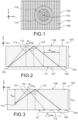
- FIG. 1 represents a top view of a part of an imaging device 100 according to a first embodiment.
- the device 100 comprises, on the same semiconductor substrate 102 comprising for example silicon and gallium nitride (GaN), a plurality of light sources 104 substantially point, corresponding here to a matrix of LEDs, and a matrix of photo-detectors 106, here photodiodes.
- the matrices of light sources 104 and photo-detectors 106 are here intertwined, that is to say that the light sources 104 are arranged within the matrix of photo-detectors 106, and the photo-detectors 106 are also arranged within the matrix of light sources 104.
- the device 100 comprises several pixels, for example forming a matrix of 88 x 88 pixels, each comprising one of the light sources 104 and one of the photo-detectors 106.
- the photodetectors 106 correspond for example to PN or PIN diodes, or to phototransistors made in the silicon of the substrate 102.
- the LEDs 104 are advantageously made from GaN transferred to the silicon of the substrate 102, this GaN being etched with so as to form the light sources 104 substantially point-like.
- the photodetectors 106 can be produced on the substrate 102 after the light sources 104.
- the substrate 102 on which the matrices of LEDs 104 and photodiodes 106 are produced is covered with an optical medium 108 (visible on the figure 2 ) which corresponds for example to a glass plate with a thickness greater than approximately 100 ⁇ m, for example of the order of 400 ⁇ m or 700 ⁇ m or even 1000 ⁇ m, and here glued to the substrate 102.
- an optical medium 108 visible on the figure 2
- the substrate 102 on which the matrices of LEDs 104 and photodiodes 106 are produced is covered with an optical medium 108 (visible on the figure 2 ) which corresponds for example to a glass plate with a thickness greater than approximately 100 ⁇ m, for example of the order of 400 ⁇ m or 700 ⁇ m or even 1000 ⁇ m, and here glued to the substrate 102.
- the optical medium 108 may comprise PMMA (whose optical index is equal to approximately 1.49), or any other suitable transparent material.
- An adhesive advantageously having the same optical index as that of the optical medium 108 (or very close to it), can be present between the optical medium 108 and the substrate 102 which comprises the LEDs 104 and the photodiodes 106. It is also possible that the optical medium 108 is molded directly on the substrate 102. Generally, the optical medium 108 is optically coupled to the substrate 102 such that there is no air between the optical medium 108 and the photodiodes 106 thus that between the optical medium 108 and the LEDs 104.
- the imaging device 100 is intended to be coupled to an electronic display device, for example a smartphone or a computer tablet. So, the matrix of LEDs 104 and photodiodes 106 form an additional device intended to be placed next to the display screen of this device, the optical medium 108 corresponding to the protective glass of this screen.
- the imaging device 100 also comprises control and reading means configured to control the light emission produced by each of the LEDs 104 and to control the detection of the light information received by the photodiodes 106.
- control and reading means comprise electronic components produced for example on the substrate 102.
- LEDs 104 are lit successively, a single LED 104 being lit at that time.
- one of the LEDs 104 is lit and is designated by the reference 110.
- This LED 110 illuminates the skin located above the optical medium 108, on an upper surface of the optical medium 108 called capture surface 109 (visible on the Figure 2 ).
- a region 112 of annular shape and formed around the LED 110 which corresponds to the center of this region 112, corresponds to the region where the light emitted by the LED 110 undergoes a total reflection or not depending on whether the skin is in contact or not with the capture surface 109.
- the region 112 is of annular shape because the LED 110 corresponds to a substantially point light source illuminating the optical medium 108 isotropically.
- the rays of light emitted by the LED 110 cross the optical medium 108 from its rear face, called detection surface 111, and which covers the LEDs 104 and the photodiodes 106, until reaching its face before forming the capture surface 109. After reaching the capture surface 109, a part of these rays (those which do not encounter skin present above the optical medium 108) are reflected against this surface and cross the medium again optical 108 to illuminate part of the photodiodes 106 on the detection surface 111.
- the reflected rays of light which will form the image intended to be detected by these photodiodes 106 are included, on the surface of detection 111, in region 114 which is also of annular shape and of larger dimensions than those of region 112.
- FIG. 1 schematically represents what is obtained from an optical point of view within the imaging device 100 when the LED 110 is lit.
- optical characteristics of the total frustrated reflection occurring at the level of the capture surface 109 of the optical medium 108 depends on the optical indices, or refractive indices, of the two media forming the interface considered, that is to say here the optical medium 108 and the external environment.
- the value of the optical index of the external environment can be considered as being equal to a fixed value, for example equal to 1.
- optical medium 108 corresponds to glass
- optical index n 108 is equal to approximately 1.51.
- the imaging device 100 is, in this first embodiment, intended to capture a fingerprint
- the optical index of the skin called n skin
- n air the optical index of the skin
- air value equal to 1
- n skin being between 1.37 and 1.4 and that of n 108 being equal to 1.51
- 65° the value of 65° will be considered below.
- the value of the second limiting angle of refraction can be calculated by considering the optical index n 108 of the optical medium 108, for example equal to 1.51 when the optical medium 108 corresponds to glass, and an additional optical index of value greater than that of the optical index of the atmosphere in which the element to be imaged is located and less than or equal to that of the optical index n skin of the element to be imaged.
- the reference 113 designates a ray of light forming, with the normal to the capture surface 109, the first limiting angle of refraction equal to 41°
- the reference 115 designates a ray of light forming, with the normal to the surface of capture 109, the second limiting angle of refraction equal to 65°.
- the values of the angles represented on the figure 2 do not entirely correspond to these values.
- the part of skin imaged when the LED 110 is lit corresponds to that located on the region 112 of the capture surface 109 of annular shape delimited by the rays 113 and 115.
- the corresponding image formed on the detection surface 111 corresponds to the region 114 of this surface which is also of annular shape and delimited by the rays 113 and 115 arriving on the detection surface 111 after a reflection against the capture surface 109.
- the system is therefore invariant by rotation around the LED 110.
- the crests of the imprint appear dark on a light background which represents the air around the imprint or the hollows of the imprint.
- the size of the image formed on the photodiodes 106 is larger than that of the portion of skin read which corresponds to region 112.
- a magnification factor greater than 1, here equal to 2 is therefore obtained with the imaging device 100. This magnification of the image is obtained without having to use optical means dedicated to this magnification.
- the distance between the rays 113 and 115 which corresponds to the difference between the external diameter and the internal diameter of the ring formed by region 112 is equal to:
- the distance between the first and second rays 113, 115 after the reflection on the capture surface 109 which corresponds to the difference between the external diameter and the internal diameter (i.e. the width) of the ring formed by region 114, is equal to:
- This magnification is equal to 2 because the rays forming the image on the photodetectors 106 travel a distance equal to twice that traveled by the rays of light between the light source and the finger whose image is captured
- the table below gives examples of dimension values obtained for the regions 112 and 114 of annular shape as a function of the thickness h of the optical medium 108, with the optical indices mentioned previously.
- the width here corresponds to the difference between the external diameter and the internal diameter of one of the regions 112 and 114.
- the size of the image of the element to be imaged obtained on the photodetectors 106 which corresponds to the detection field obtained when one of the light sources 104 is turned on, is therefore twice as large as that of the skin region 112 corresponding to this image, and is proportional to the thickness h of the optical medium 108.
- the light sources 104 and the photodetectors 106 are produced on the same substrate 102 and are arranged at the same distance h from the capture surface 109 which corresponds to the thickness of the medium optical 108. This distance h is chosen such that it is greater than the pitch of the photo-detector matrix 106 so that the imaging device 100 does not operate in the near field.
- the light sources 104 and the photo-detectors 106 are not arranged at the same distance from the capture surface 109.
- Figure 3 schematically represents such a configuration.
- the arrays of light sources 104 and photodetectors 106 can be seen as being intertwined but arranged on different levels.
- h pho designates the material thickness of the optical medium 108 between the photodetectors 106 and the capture surface 109
- h led designates the material thickness of the optical medium 108 between the light sources 104 and the capture surface 109.
- R picture h led + h pho . tan VS skin/glass ⁇ h led + h pho . tan VS air/glass
- R picture h led + h pho . tan 65 ° ⁇ tan 41 ° .
- This magnification G therefore only depends on the geometric parameters of the imaging device 100 and does not depend on the quality of the material of the optical medium 108 or the nature of the element to be imaged. This magnification G is here always greater than 1. Thus, the resolution of the image captured by the photodetectors 106 is greater than that of the photo-detector matrix 106 itself, and this without using dedicated optical magnification means.
- the value of the magnification G can be modified for example by varying the values of h pho and h led .
- the value of the magnification G can be brought closer to the value 1 by increasing, for example, the value of h led .
- the value of the magnification G can be increased by, for example, increasing the value h pho .
- regions 112 and 114 are represented such that they do not overlap. However, in reality, considering the limit refraction angle values of 41° and 65°, these regions 112 and 114 partially overlap, that is to say that the value of the external diameter of the annular region corresponding to region 112 is less than that of the internal diameter of the annular region corresponding to region 114.
- the number of light sources 104 to be lit, and therefore the number of the images to be captured is for example chosen according to the dimensions of the capture zone which corresponds for example to a square whose dimensions can be chosen according to the needs and/or the design of the acquisition system, for example 5mm ⁇ 5mm or 12.8mm ⁇ 12.8mm.
- the optical parameters described above relating to the light reflections occurring in the device 100 can be determined in advance (values of R skin , R image , locations of regions 112 and 114, etc.), it is possible to know , for each light source 104 which will be lit, the photo-detectors 106 which will be part of the region 114 associated with the light source 104 which is lit. It is therefore not necessary that when each light source 104 is switched on, all the photo-detectors 106 of the imaging device 100 carry out an acquisition. Only photodetectors 106 included in region 114, or forming for example a square or rectangle including region 114, can carry out this acquisition. It is also possible that photodetectors 106 carrying out the acquisition are those included in a region smaller than region 114. A larger number of acquisitions must in this case be carried out.
- This compensation can be carried out either from a predefined model, or by first carrying out an empty acquisition with the device 100 (without a finger on the capture surface 109).
- the different light sources 104 lit successively are chosen such that the regions 112 captured together cover the entire surface of the element to be imaged.
- several light sources 104 each allowing the acquisition of an image
- this for several lines of the pixel matrix it is possible to cover a major part of this surface of the element to be captured.
- the imaging device 100 described above in connection with the figure 1 may include photodiodes 106 and LEDs 104 made in CMOS technology.
- the LEDs 104 can advantageously be made from GaN transferred to the silicon substrate 102 comprising the photodetectors 106 made in CMOS (as well as the reading electronics, or even the processing electronics).
- the photo-detectors 106 and the light sources 104 form pixels for example (each pixel comprising a photo-detector 106, a light source 104 such as an LED of size equal to 10 ⁇ 10 ⁇ m 2 or 3 ⁇ 3 ⁇ m 2 , transistors, etc.) of dimension equal to 50 ⁇ 50 ⁇ m 2 .
- a magnification G equal to 2
- the resolution of the final image obtained is equivalent to 1000 ppi while the resolution of the pixels of the imaging device 100 is 500 ppi.
- the capture region 112 of the imaging device 100 can correspond to a square of dimension equal to 3000 ⁇ 3000 ⁇ m 2 .
- an LED 104 every 8 pixels (in order to have a capture offset corresponding to half the width of the ring formed by region 112), or even every 9 or 10 pixels, so that the partial images obtained together form part of the final image corresponding to this line of pixels.
- an LED 104 every 8 pixels (in order to have a capture offset corresponding to half the width of the ring formed by region 112), or even every 9 or 10 pixels, so that the partial images obtained together form part of the final image corresponding to this line of pixels.
- only one line of pixels out of 50, or 55 or even 60 is sufficient to obtain all the partial images allowing the reconstruction of the final image including the entire capture surface.
- Other steps and other capture/detection region sizes are possible, sufficient overlap of the images allowing the final image to be obtained.
- FIG. 4 represents the regions 112 and 114 obtained in the particular configuration described above (magnification G equal to 2, optical medium 108 corresponding to a glass plate with a thickness equal to 700 ⁇ m).
- the skin region located on the capture surface 109 and which is intended to be detected here corresponds to a square of dimensions equal to 4.4 ⁇ 4.4 mm 2 referenced 116.
- regions 112 and 114 partially overlap at a region referenced 117.
- these regions 112 and 114 represented on the Figure 4 correspond to those obtained with a lit light source 110 positioned in the upper right corner of the region 116 to be imaged.
- the Figure 4 illustrates the fact that the corners of region 116 cannot be detected by the photo-detectors 106 located in region 116 because even by turning on the light sources located in these corners, the latter are illuminated by rays forming, with the capture surface 109, an angle of incidence less than the first limiting angle of refraction.
- FIG. 5 schematically represents part of the regions 112 imaged during a capture of these upper and lower bands of region 116.
- the light sources 104 which are lit are chosen so that each of the different regions 112 captured has an overlap with one or more other regions 112.
- Capturing a central band of region 116 can be achieved by lighting the light sources 104 (for example one every 8 pixels) of a line located substantially in the center of region 116.
- FIG. 6 represents the parts of region 116 captured at this stage and which correspond to 36 partial images of the print.
- References 118, 120 and 122 respectively designate the lower, upper and central bands of region 116 (with a slight overlap between parts 118 and 122, as well as between parts 120 and 122).
- the reference 124 designates the corners of the regions 116 as well as the parts of the edges of the central region 122 which are not captured during the reading of the three bands 118, 120 and 122.
- the parts 124 of the edges of the central region 122 not captured by the steps implemented previously can be captured by lighting light sources 104, for example four in number, located at the edges of the region 122.
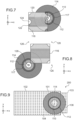
- Figure 7 represents the regions 112 and 114 obtained by lighting one of these light sources, referenced 110 on the Figure 7 , and which makes it possible to partially capture one of these parts 124 not initially captured during the acquisition of the central band 122. At this stage of the acquisition, 40 partial images of the print have been obtained.
- the imaging device 100 comprises, in addition to the matrix of light sources 104, at least four additional light sources 126 located outside of the matrix formed by the light sources 104, and each arranged along a bisector of the angle of one of the other corners of the region 116.
- figure 8 represented schematically these four LEDs 126 which make it possible to acquire the corners of the region 116.
- each of the additional light sources 126 is for example arranged at a distance equal to approximately 600 ⁇ m from the corner closest to the matrix.
- additional light sources 126 are arranged along each of the bisectors of the corner angles of the light source array 104, at different distances from these corners.
- the additional light source 126 located at the appropriate distance from the matrix to carry out this acquisition.
- region 116 Other methods of reading region 116 than that described above are possible. For example, it is possible that when each of the light sources 104 is switched on, only part of the region 114 is read by the photodetectors 106, for example one or more square-shaped parts included in the region 114, or even only one or a few photo-detectors 106 included in region 114.
- the ignition sequence of the light sources 104 is in this case adapted in order to have a certain overlap between the different images captured.
- each of the pixels (which includes a light source 104 and a photodetector 106) has a dimension equal to approximately 50 ⁇ m ⁇ 50 ⁇ m 2 .
- These dimensions can be different: for example each pixel can have dimensions equal to approximately 25 ⁇ m ⁇ 25 ⁇ m, or even equal to 12.5 ⁇ m ⁇ 12.5 ⁇ m.
- FIG. 12 represents a top view of the imaging device 100, here according to the first embodiment, on which the control and reading means configured to successively turn on and turn off each of the light sources 104 and, during the ignition of each of the light sources 104, to read the photo-detectors 106 and control the acquisition by the photo-detectors 106 of a partial image of the element to be imaged are visible.
- These control means comprise, for example here, circuits 136 for addressing the light sources 104 and the photo-detectors 106.
- the imaging device 100 also comprises means 138 for processing the information captured by the photo-detectors 106. These means 138 are for example those constructing the different partial images obtained then calculating the final image of the captured print, from the different partial images.
- the imaging device 100 also includes a control element 140 connected to the circuits 136 and to the means 138 and controlling these elements.
- FIG. 9 represents an imaging device 200 according to another exemplary embodiment.
- the array of photo-detectors 106 of the imaging device 200 is arranged next to each other. of the matrix of light sources 104, in a sensor part 103 of the device 200 distinct from a display part 101 of the device 200.
- the display part 101 can correspond to a screen of an electronic device, for example a smartphone, to edge of which the sensor part 103 is arranged.
- the sensor part 103 may or may not be juxtaposed with the display part 101.
- the regions 112 and 114 obtained during the ignition of one of the light sources 104, referenced 110 in this figure, are represented.
- By lighting several light sources 104 of the same column as the light source 110 it is possible to capture a region of the element to be imaged located on the display part 101, at the level of the edge juxtaposed to the sensor part 103.
- An additional capture can also be carried out by using the light sources 104 of one or more other columns of the display part 101, this or these columns remaining close to the sensor part 103 so that the region 114 is found at least partially on the sensor part 103.
- optical medium 108 By using as optical medium 108 a glass plate with a thickness equal to approximately 700 ⁇ m, it is possible to obtain a region 114 with a width equal to approximately 1725 ⁇ m (which corresponds to 34 pixels each with a width equal to 50 ⁇ m). when a single column of light sources 104 is used. In this configuration, the distance between the light sources 104 of the column used and the region 114 is equal to 1217 ⁇ m.
- a thick optical medium 108 for example obtained by superimposing two (or more) glass slides, allowing for example the obtaining of an optical medium 108 of greater thickness or equal to 1 mm.
- the sensor part 103 is arranged next to the display part 101.
- the display part 101 is made such that it forms an at least partially transparent screen, that is to say capable of being crossed by a part of the light received, the sensor part 103 can be placed under this screen.
- the arrays of light sources and photodetectors can be seen as being intertwined but arranged on different levels.
- the device 200 is preferably such that the display part 101 is produced with light sources 104 of the OLED type, and advantageously such that the emission of light is carried out through the substrate 102 (for example made of glass) on which the light sources 104 are carried out ("bottom emission", or emission from the rear) and through the optical medium 108.
- the transparent conductive tracks, comprising for example ITO, of the substrate 102 on which the light sources 104 are made can be used to connect the sensor part 103.
- the upper metal levels can also be used.
- the device 200 such that transparent holes are present within the display part 101, the sensor part 103 being able in this case to be transferred to the display part 101 by arranging the photo-detectors 106 facing the holes transparent.
- FIG. 10 represents the imaging device 100 according to a second embodiment.
- the optical medium 108 corresponds to the transparent substrate used for the production of TFT transistors used for addressing the pixels of the device 100, and which form part of the control means of the imaging device 100.
- the reference 128 designates the assembly formed on the side of the detection surface 111 and which comprises the addressing TFT transistors, the OLED type light sources 104 emitting their light on the side of their rear face, and the photo-detectors 106 which are for example PIN photodiodes.
- One or more electronic chips 130 controlling for example the ignition of the light sources 104 and/or the reading by the photo-detectors 106 are also arranged on the side of the detection surface 111, next to the assembly 128.
- the The other face of the substrate forming the optical medium 108 remains free and forms the capture surface 109 on which the element to be imaged, typically a finger, is intended to be located.
- An interconnection layer 132 is present between the optical medium 108 and these elements 128, 130.
- the optical medium 108 may have a thickness greater than or equal to approximately 1 mm, for example between approximately 1 mm and 2 mm.
- a thick optical medium 108 is for example obtained by gluing several blades of the same optical index with an adhesive, or glue, also having this same optical index so as not to have any reflection at the interface formed by the glue.
- the OLED type light sources 104 can emit light from their front face, the emitted light only passing through the optical medium 108 reported on these light sources 104 and not the substrate 102.
- the device 100 according to this second embodiment can be such that it is of large dimensions and configured to carry out simultaneous capture of the fingerprints of several fingers or even of an entire hand.
- an optical medium 108 of significant thickness for example greater than approximately 1 mm, ensures a certain solidity to the device 100.
- FIG. 11 represents the technological stack produced to form such an assembly 128.
- the reference 133 designates the face of this assembly 128 which is intended to be on the side of the optical medium 108.
- a part 134 comprising addressing TFT transistors 135 is made from polycrystalline silicon. These TFT 135 transistors can also be made from amorphous silicon or IGZO. Polycrystalline silicon is preferably used because it allows better electrical performance to be obtained, which makes it possible to reduce the size of the TFT transistors.
- This part 134 also includes the different electrical interconnection lines of the imaging device 100.
- the stack of layers forming the photodetectors 106 is then formed on part 134.
- Amorphous silicon can advantageously be used to produce these PIN diodes.
- the electrodes of the PIN diodes located on the side of the TFT transistors can be formed by a conductive layer dedicated to these electrodes, or be formed within a level of metal common to the transistors.
- the electrodes of the PIN diodes located on the side of the light sources 104 are made from an electrically conductive material and for example opaque.
- a planarizing insulating material 137 is then deposited on the assembly produced, forming a flat surface on which the OLED type light sources 104 are then produced.
- the production of OLED type diodes includes in particular the implementation of a deposition and lithography of a conductive material to form the anodes, then the deposition of emissive organic layers, and the production of a cathode common to the diodes. .
- Producing the OLED diodes after the other elements of the imaging device 100 makes it possible to not expose the materials used to form the OLED diodes to the temperatures and solvents used for the production of the previous elements.
- the OLED structure produced is transparent, with for example a metallic layer forming a mirror placed on the cathode to reflect the light, and the light emission produced can be monochrome (any wavelength of the entire visible range, UV and IR), or white thanks to a vertical stack of two or three emitted colors.
- An encapsulation material 139 is then deposited on the assembly produced.
- TFT transistors can be arranged on the periphery of the matrix of light sources 104 and photodetectors 106 to form the means used for control and/or reading and thus limit the number of inputs/outputs to be made to the circuits external controls made in silicon technology, for example in CMOS.
- each light source 104 of the OLED type can be controlled by two TFT transistors (a first to select the pixel, and a second to supply the OLED diode) in the case of an active matrix (AMOLED solution), or else be controlled by a passive matrix forming a grid with rows and columns of conductive lines allowing the OLED diode to switch on when the voltage Ignition is applied to the row and column corresponding to this diode (PMOLED solution).
- Each PIN diode type photodetector 106 can be controlled by another TFT transistor (in the case of so-called passive reading), or by several other TFT transistors in the case of so-called active reading.
- the value of the second limiting angle of refraction is obtained by considering a skin optical index equal to 1.37.
- a skin optical index equal to 1.37.
- the photo-detectors 106 intended to receive the rays forming the outer edge of the region 114
- this estimation then being used to verify that these optical indices correspond to that of the air (optical index equal to 1) and the skin (optical index of value within a predetermined range).
- This makes it possible to detect whether the skin illuminated by this light source corresponds to real skin, or whether this skin is artificial.
- the imaging device 100 is therefore well suited to carry out fraud detection when this device 100 is used as a fingerprint sensor. It is also possible to estimate the optical index of the imaged element from the dimensions of region 114.
- the optical medium 108 can correspond to several superimposed layers of transparent material.
- the smartphone in which the imaging device 100 is produced initially comprises a glass of thickness less than that desired for proper operation of the imaging device 100, it is possible to add an additional protective glass making it possible to form, with the initial glass, an optical medium 108 having the desired thickness.
- the materials used to form the optical medium 108, the additional protective glass and the glue between these two elements are chosen so that their optical indices are as close as possible to each other in order to limit reflections to the maximum. interfaces of these different elements.
- the senor 100 it is possible for the sensor 100 to include a filtering system making it possible to limit or avoid disturbances which would be due to the illumination of the sensor 100 by light external to it.
- This filtering system can correspond for example to a pair of polarizing filters, or wavelength filters or even angular filters allowing only light rays having a certain angle of incidence value to pass.
- the senor 100 can be used to perform a static fingerprint capture, that is to say with a finger not moving on the optical medium 108, or to form a sensor scanning, that is to say adapted to capture the imprint of a moving finger on the optical medium 108.
- a scanning sensor a smaller number of light sources 104 can be used by compared to a static fingerprint sensor because the image does not need to have a large dimension in the direction of movement of the finger.
- the movement of the element to be imaged made between the capture of each of the partial images will be calculated and taken into account. To construct the final image, a partial image capture is sufficient because the finger moves between two partial image acquisitions.
- the imaging device 100 can be used advantageously to form a fingerprint sensor, it is also possible to use the imaging device 100 as a device for detecting movement of the element to be imaged to form, for example, a pointing device, or touchpad.
- the photodetectors 106 of the imaging device 100 used during image capture receive a significant quantity of light coming from the light sources 104.
- the integration times of the imaging device 100 are short.
- the imaging device 100 forms a sensor having a pixel resolution of 500 ppi
- the acquisition of the complete image is carried out in a little less than 50 ms.
- the device 100 remains functional even if certain pixels no longer work. For example, if a faulty pixel corresponds to one of those whose LED is not intended to be lit to capture part of the fingerprint, then the information not captured by this pixel can be obtained from another image partially covering the one comprising the faulty pixel. If the faulty pixel corresponds to one of those whose LED is intended to be lit to capture part of the fingerprint, it is possible to call on a neighboring pixel whose LED can be lit and perform a capture of the fingerprint. part of the imprint.
- these light sources 104 which are sufficiently distant and lit simultaneously are arranged on the same line, which makes it possible to reduce the overall duration of capture of the element to be imaged when the imaging device 100 is configured to read all the pixels of the same line simultaneously.
- each pixel can comprise one of the light sources 104 and one of the photo-detectors 106.
- each pixel comprises either a light source 104 or a photo-detector 106.
- each pixel of the final image can be seen by several photo-detector/light source couples, it there is redundancy in the captured information and it is therefore not necessary to have a photo-detector/light source pair within each of the pixels of the device 100.
- the capture carried out by the imaging device 100 makes it possible to obtain a final monochrome image, the light sources 104 being able to be produced such that they emit light at the same wavelength (for example red or green).
- the formation of the image does not depend or only slightly on the wavelength of the light.
- the imaging device 100 such that the acquired image is in color via the use of light sources 104 emitting lights of different colors.
- light sources 104 emitting lights of different colors.
- a first line of light sources 104 can emit green light
- a second line of light sources 104 can emit red light
- a third line of light sources 104 can emit blue light, and this for all the lines of the matrix of light sources 104.
- the light sources 104 can be shared between several photo-detectors 106 arranged side by side, for example by producing each light sources 104 at the center of a group of four pixels each comprising a photo-detector 106.
- each pixel such that it comprises a photo-detector 106 and three light sources 104 each configured to emit red light, green or blue.
- the sensor part of the imaging device 100 forms a color display which can blend in, for example, with the rest of the screen of the smartphone in which the imaging device 100 is integrated.
- an imaging device 100 serving for example as a “flash”, that is to say configured to emit high intensity white light.
- an imaging device 100 can in this case be placed on the rear side of the electronic device of the smartphone type, this flash being used for example when taking a photograph.
- the capture surfaces 109 and detection surfaces 111 formed by the upper and lower faces of the optical medium 108 are substantially planar. It is however possible to consider having at least one of these surfaces, in particular the capture surface 109, which is concave or convex. In this case it is appropriate to take into account the radius of curvature of this face which influences the reflection of the light rays on this face, and therefore the choice of photo-detectors 106 to be used for the acquisition of each of the partial images of the element to be imaged, as well as the associated magnification or distortion factors. As these parameters are stable, a calibration of the system can advantageously be implemented in production.
- the light emission angle of the LEDs for example via the deposition of a layer of low optical index in front of the finger, such as the limiting angle between this layer and the glass matches the desired angle value.
- Such control can for example be used to simultaneously turn on two light sources which are not far enough apart so as not to interfere with each other.
Landscapes
- Engineering & Computer Science (AREA)
- Inorganic Chemistry (AREA)
- Chemical & Material Sciences (AREA)
- Physics & Mathematics (AREA)
- Theoretical Computer Science (AREA)
- Multimedia (AREA)
- General Physics & Mathematics (AREA)
- Human Computer Interaction (AREA)
- Life Sciences & Earth Sciences (AREA)
- Sustainable Development (AREA)
- Optics & Photonics (AREA)
- Image Input (AREA)
- Studio Devices (AREA)
- Facsimile Heads (AREA)
- Facsimile Scanning Arrangements (AREA)
Claims (14)
- Optische Abbildungsvorrichtung (100), die mindestens Folgendes umfasst:- ein Array von Lichtquellen (104), die auf einem Substrat (102) hergestellt werden und einen Anzeigebildschirm bilden,- ein Array von Fotodetektoren (106), die auf dem Substrat (102) hergestellt und mit dem Array von Lichtquellen (104) verschachtelt sind,- ein optisches Medium (108), das die Lichtquellen (104) und die Fotodetektoren (106) abdeckt und durch das sich Licht ausbreiten kann, das dazu bestimmt ist, von den Lichtquellen (104) emittiert zu werden, und eine Erfassungsoberfläche (109), an der ein abzubildendes Element dazu bestimmt ist, angeordnet zu werden, und eine Detektionsoberfläche (111) bildet, die im Wesentlichen parallel zur Erfassungsoberfläche (109) verläuft und an der die Arrays von Lichtquellen (104) und von Fotodetektoren (106) angeordnet sind,dadurch gekennzeichnet, dass das optische Medium (108) eine Dicke aufweist, die größer ist als der Abstand der Fotodetektoren (106) des Arrays von Fotodetektoren (106),und dadurch, dass die optische Abbildungsvorrichtung (100) ferner eine Steuer- und Leseeinrichtung (134, 136, 138, 140) umfasst, die dazu konfiguriert ist, nacheinander jeden Teil der Lichtquellen (104) ein- und auszuschalten und während des Einschaltens jedes Teils der Lichtquellen (104) mindestens einen Teil der Fotodetektoren (106) auszulesen, die dazu bestimmt sind, Lichtstrahlen (113, 115) zu empfangen, die von der eingeschalteten Lichtquelle (104) ausgegeben werden und an der Erfassungsoberfläche (109) reflektiert wurden, indem mit der Erfassungsoberfläche (109) ein Einfallswinkel gebildet wird, der in Abhängigkeit von dem optischen Medium (108) und dem abzubildenden Element geschätzt wird,und dadurch, dass jede der Lichtquellen (104) dazu konfiguriert ist, auf der Detektionsoberfläche (111) einen Bereich (114) zu bilden, dessen Größe mindestens doppelt so groß ist wie die Größe einer emittierenden Oberfläche der Lichtquelle,und dadurch, dass der Wert des Einfallswinkels zwischen dem eines ersten Grenzbrechungswinkels, der durch den optischen Index des optischen Mediums (108) und den optischen Index der Atmosphäre, in der sich das abzubildende Element befindet, definiert ist, und dem eines zweiten Grenzbrechungswinkels, der durch den optischen Index des optischen Mediums (108) und einen zusätzlichen optischen Index mit einem Wert, der größer ist als der des optischen Index der Atmosphäre, in der sich das abzubildende Element befindet, und kleiner als der oder gleich dem des optischen Index des abzubildenden Elements ist, definiert ist, liegt oder diesem entspricht.
- Optische Abbildungsvorrichtung (100) nach Anspruch 1, wobei die Steuer- und Leseeinrichtung (134,136,138,140) dazu konfiguriert ist, während des Einschaltens jedes Teils der Lichtquellen (104) die Fotodetektoren (106) auszulesen, die sich im Bereich (114) der Detektionsoberfläche (111) befinden, der ringförmig ist und von den reflektierten Lichtstrahlen (113, 115) begrenzt wird, die an der Erfassungsoberfläche (109) den ersten und den zweiten Grenzbrechungswinkel bilden.
- Optische Abbildungsvorrichtung (100) nach einem der vorhergehenden Ansprüche, wobei die Steuer- und Leseeinrichtung (134, 136, 138, 140) so konfiguriert sind, dass die beim Einschalten jedes Teils der Lichtquellen (104) ausgelesenen Fotodetektoren (106) ein Teilbild des abzubildenden Elements liefern, so dass sich jedes der erhaltenen Teilbilder mindestens teilweise mit einem anderen Teilbild des abzubildenden Elements überlappt.
- Optische Abbildungsvorrichtung (100) nach Anspruch 3, die ferner eine Einrichtung zum Berechnen eines endgültigen Bilds des abzubildenden Elements aus Teilbildern des abzubildenden Elements umfasst.
- Optische Abbildungsvorrichtung (100) nach einem der vorhergehenden Ansprüche, die ferner zusätzliche Lichtquellen (126) umfasst, die außerhalb des Arrays von Lichtquellen (104) angeordnet und auf Halbierende der Winkel ausgerichtet sind, die durch die Ecken des Arrays von Lichtquellen (104) gebildet werden.
- Optische Abbildungsvorrichtung (100) nach einem der vorhergehenden Ansprüche, wobei jedes Pixel des Anzeigebildschirms eine der Lichtquellen (104) und einen der Fotodetektoren (106) umfasst.
- Optische Abbildungsvorrichtung (100) nach einem der vorhergehenden Ansprüche, wobei die Lichtquellen (104) durch LEDs gebildet sind und die Steuer- und Leseeinrichtung (134, 136, 138, 140) CMOS-Transistoren umfasst, oder wobei die Lichtquellen (104) vom OLED-Typ sind und die Steuer- und Leseeinrichtung (134, 136, 138, 140) TFT-Transistoren umfasst, die verschachtelt mit dem Array von Fotodetektoren (106) angeordnet sind.
- Optische Abbildungsvorrichtung (100) nach Anspruch 7, wobei, wenn die Lichtquellen (104) vom OLED-Typ sind und die Steuer- und Leseeinrichtung (134, 136, 138, 140) TFT-Transistoren umfasst, die TFT-Transistoren auf dem Substrat (102) hergestellt sind, das transparent ist und das optische Medium (108) bildet.
- Optische Abbildungsvorrichtung (100) nach einem der vorhergehenden Ansprüche, wobei die Dicke des optischen Mediums (108) größer ist als 50 µm, oder wobei das optische Medium (108) eine Glasplatte mit einer Dicke von größer gleich 700 µm umfasst.
- Bilderfassungsverfahren, das von einer optischen Abbildungsvorrichtung (100) durchgeführt wird, die mindestens Folgendes umfasst:- ein Array von Lichtquellen (104), die auf einem Substrat (102) hergestellt werden und einen Anzeigebildschirm bilden,- ein Array von Fotodetektoren (106), die auf dem Substrat (102) hergestellt und mit dem Array von Lichtquellen (104) verschachtelt sind,- ein optisches Medium (108), das die Lichtquellen (104) und die Fotodetektoren (106) abdeckt und durch das sich Licht ausbreiten kann, das dazu bestimmt ist, von den Lichtquellen (104) emittiert zu werden, und eine Erfassungsoberfläche (109), an der ein abzubildendes Element dazu bestimmt ist, angeordnet zu werden, und eine Detektionsoberfläche (111) bildet, die im Wesentlichen parallel zur Erfassungsoberfläche (109) verläuft und an der die Arrays von Lichtquellen (104) und von Fotodetektoren (106) angeordnet sind,dadurch gekennzeichnet, dass das optische Medium (108) eine Dicke aufweist, die größer ist als der Abstand der Fotodetektoren (106) des Arrays von Fotodetektoren (106),und dadurch, dass jede der Lichtquellen (104) der optischen Abbildungsvorrichtung (100) dazu konfiguriert ist, auf der Detektionsoberfläche (111) einen Bereich (114) zu bilden, dessen Größe mindestens doppelt so groß ist wie die Größe einer emittierenden Oberfläche der Lichtquelle,wobei das Bilderfassungsverfahren das Durchführen der folgenden Schritte durch die Steuer- und Leseeinrichtung (134, 136, 138, 140) der optischen Abbildungsvorrichtung (100) umfasst:a) Einschalten einer der Lichtquellen (104),b) Auslesen mindestens eines Teils der Fotodetektoren (106), die Lichtstrahlen (113, 115) empfangen, die von der eingeschalteten Lichtquelle (104) ausgegeben werden und an der Erfassungsoberfläche (109) reflektiert wurden, indem mit der Erfassungsoberfläche (109) ein Einfallswinkel gebildet wird, der in Abhängigkeit von dem optischen Medium (108) und dem abzubildenden Element geschätzt wird,c) Ausschalten der eingeschalteten Lichtquelle (104),wobei die Schritte a) bis c) für jeden Teil der Lichtquellen (104) wiederholt werden,und dadurch, dass der Wert des Einfallswinkels zwischen dem eines ersten Grenzbrechungswinkels, der durch den optischen Index des optischen Mediums (108) und den optischen Index der Atmosphäre, in der sich das abzubildende Element befindet, definiert ist, und dem eines zweiten Grenzbrechungswinkels, der durch den optischen Index des optischen Mediums (108) und einen zusätzlichen optischen Index mit einem Wert, der größer ist als der des optischen Index der Atmosphäre, in der sich das abzubildende Element befindet, und kleiner als der oder gleich dem des optischen Index des abzubildenden Elements ist, definiert ist, liegt oder diesem entspricht.
- Verfahren nach Anspruch 10, wobei die Fotodetektoren (106), die während des Schritts b) ausgelesen werden, diejenigen sind, die sich im Bereich (114) der Detektionsoberfläche (111) befinden, der ringförmig ist und von den reflektierten Lichtstrahlen (113, 115) begrenzt wird, die an der Erfassungsoberfläche (109) den ersten und den zweiten Grenzbrechungswinkel bilden.
- Verfahren nach einem der Ansprüche 10 oder 11, wobei die Fotodetektoren (106), die während jedes Durchführens des Schritts b) ausgelesen werden, ein Teilbild des abzubildenden Elements liefern, so dass sich jedes der erhaltenen Teilbilder mindestens teilweise mit einem anderen Teilbild des abzubildenden Elements überlappt.
- Verfahren nach Anspruch 12, das ferner das Durchführen eines Schritts des Berechnens eines endgültigen Bilds des abzubildenden Elements aus den Teilbildern des abzubildenden Elements umfasst.
- Verfahren nach einem der Ansprüche 10 bis 13, wobei die Schritte a) bis c) ebenfalls für die zusätzlichen Lichtquellen (126) durchgeführt werden, die außerhalb des Arrays von Lichtquellen (104) angeordnet und auf Halbierende der Winkel ausgerichtet sind, die durch die Ecken des Arrays von Lichtquellen (104) gebildet werden.
Applications Claiming Priority (1)
| Application Number | Priority Date | Filing Date | Title |
|---|---|---|---|
| FR1752160A FR3064112B1 (fr) | 2017-03-16 | 2017-03-16 | Dispositif imageur optique |
Publications (2)
| Publication Number | Publication Date |
|---|---|
| EP3376544A1 EP3376544A1 (de) | 2018-09-19 |
| EP3376544B1 true EP3376544B1 (de) | 2024-05-01 |
Family
ID=59253647
Family Applications (1)
| Application Number | Title | Priority Date | Filing Date |
|---|---|---|---|
| EP18161920.6A Active EP3376544B1 (de) | 2017-03-16 | 2018-03-15 | Optische bildanzeigevorrichtung |
Country Status (4)
| Country | Link |
|---|---|
| US (1) | US10381387B2 (de) |
| EP (1) | EP3376544B1 (de) |
| CN (1) | CN108629269B (de) |
| FR (1) | FR3064112B1 (de) |
Families Citing this family (13)
| Publication number | Priority date | Publication date | Assignee | Title |
|---|---|---|---|---|
| FR3054698B1 (fr) | 2016-07-29 | 2018-09-28 | Commissariat A L'energie Atomique Et Aux Energies Alternatives | Capteur de motif thermique actif comprenant une matrice passive de pixels |
| US10664676B2 (en) * | 2017-06-12 | 2020-05-26 | Will Semiconductor (Shanghai) Co. Ltd. | Systems and methods for reducing unwanted reflections in display systems incorporating an under display biometric sensor |
| TWI666753B (zh) * | 2017-09-28 | 2019-07-21 | 致伸科技股份有限公司 | 光學指紋感測單元及其製造方法 |
| US10474860B2 (en) * | 2017-09-29 | 2019-11-12 | Apple Inc. | Electronic device including a display driven based upon first and second alternatingly read memories and related methods |
| CN110895824B (zh) * | 2018-09-12 | 2023-03-28 | 上海耕岩智能科技有限公司 | 确定显示屏幕厚度参数的方法、存储介质及电子设备 |
| CN109543558B (zh) * | 2018-10-30 | 2023-12-26 | Oppo广东移动通信有限公司 | 指纹图像处理方法及相关产品 |
| CN109583420B (zh) * | 2018-12-14 | 2021-02-05 | 京东方科技集团股份有限公司 | 指纹识别装置的驱动方法及设备 |
| CN111722816B (zh) * | 2019-03-19 | 2024-12-27 | 上海耕岩智能科技有限公司 | 可弯折屏的成像比例的确定方法、电子设备、存储介质 |
| EP4032008A4 (de) * | 2019-09-17 | 2022-09-07 | BOE Technology Group Co., Ltd. | Lichterfassende detektionsvorrichtung, anzeigevorrichtung, verfahren zur fingerabdruckdetektion und verfahren zum betrieb einer anzeigevorrichtung |
| CN110650278A (zh) * | 2019-10-12 | 2020-01-03 | Oppo广东移动通信有限公司 | 一种图像传感器、摄像头模组及电子设备 |
| CN111128046B (zh) * | 2020-01-16 | 2021-04-27 | 浙江大学 | 一种led显示屏幕的无透镜成像装置及方法 |
| CN112378894A (zh) * | 2020-12-10 | 2021-02-19 | 河南师范大学 | 一种多功能瞬态电致发光测量系统 |
| FR3127073B1 (fr) * | 2021-09-13 | 2024-01-19 | Commissariat Energie Atomique | Dispositif optoelectronique a composants emissif et photodetecteur superposes |
Family Cites Families (21)
| Publication number | Priority date | Publication date | Assignee | Title |
|---|---|---|---|---|
| US5101099A (en) * | 1990-06-15 | 1992-03-31 | Fuji Xerox Co., Ltd. | Image reading device with different reflectivity coefficients in a transparent layer and a substrate |
| US5627364A (en) * | 1994-10-11 | 1997-05-06 | Tdk Corporation | Linear array image sensor with thin-film light emission element light source |
| GB9509499D0 (en) * | 1995-05-10 | 1995-07-05 | Ultra Silicon Techn Uk Ltd | Optical read and write systems |
| SE9700384D0 (sv) * | 1997-02-04 | 1997-02-04 | Biacore Ab | Analytical method and apparatus |
| JP2001351820A (ja) | 2000-06-07 | 2001-12-21 | Mitsubishi Electric Corp | 電気機器 |
| US6747290B2 (en) * | 2000-12-12 | 2004-06-08 | Semiconductor Energy Laboratory Co., Ltd. | Information device |
| JP4759511B2 (ja) * | 2004-04-19 | 2011-08-31 | 株式会社日立製作所 | 撮像機能一体型表示装置 |
| DE102004020661A1 (de) * | 2004-04-24 | 2005-11-17 | Smiths Heimann Biometrics Gmbh | Anordnung und Verfahren zum Prüfen von optischen Beugungsstrukturen auf Dokumenten |
| JP2010153449A (ja) * | 2008-12-24 | 2010-07-08 | Seiko Epson Corp | 光源一体型光電変換装置 |
| EP2633277B1 (de) * | 2010-10-27 | 2020-06-17 | Cornell University | Winkelempfindliche pixelvorrichtung |
| FR2980277B1 (fr) * | 2011-09-20 | 2013-10-11 | Commissariat Energie Atomique | Fibre optique microstructuree a grand coeur et a mode fondamental aplati, et procede de conception de celle ci, application a la microfabrication par laser |
| FR3016115B1 (fr) | 2014-01-06 | 2016-02-05 | Commissariat Energie Atomique | Recipient interagissant avec un utilisateur a consommation energetique reduite avant deballage |
| US9836165B2 (en) | 2014-05-16 | 2017-12-05 | Apple Inc. | Integrated silicon-OLED display and touch sensor panel |
| US9436866B2 (en) * | 2014-08-01 | 2016-09-06 | General Electric Company | High sensitivity flat panel microbiology detection and enumeration system |
| EP3278272B1 (de) * | 2015-06-18 | 2020-12-09 | Shenzhen Goodix Technology Co., Ltd. | Multifunktionsfingerabdrucksensor mit optischer abtastfähigkeit |
| FR3054696B1 (fr) | 2016-07-29 | 2019-05-17 | Commissariat A L'energie Atomique Et Aux Energies Alternatives | Capteur de motif thermique a elements chauffants mutualises |
| FR3054697B1 (fr) | 2016-07-29 | 2019-08-30 | Commissariat A L'energie Atomique Et Aux Energies Alternatives | Procede de capture de motif thermique a chauffage optimise des pixels |
| FR3065306B1 (fr) * | 2017-04-12 | 2019-04-05 | Safran Identity and Security | Procede de detection de fraude |
| CN107066162B (zh) * | 2017-05-27 | 2020-03-17 | 上海天马微电子有限公司 | 一种显示面板及显示装置 |
| CN107133613B (zh) * | 2017-06-06 | 2020-06-30 | 上海天马微电子有限公司 | 一种显示面板及显示装置 |
| US10664676B2 (en) * | 2017-06-12 | 2020-05-26 | Will Semiconductor (Shanghai) Co. Ltd. | Systems and methods for reducing unwanted reflections in display systems incorporating an under display biometric sensor |
-
2017
- 2017-03-16 FR FR1752160A patent/FR3064112B1/fr active Active
-
2018
- 2018-03-15 CN CN201810214172.7A patent/CN108629269B/zh active Active
- 2018-03-15 EP EP18161920.6A patent/EP3376544B1/de active Active
- 2018-03-15 US US15/922,204 patent/US10381387B2/en active Active
Also Published As
| Publication number | Publication date |
|---|---|
| FR3064112A1 (fr) | 2018-09-21 |
| CN108629269B (zh) | 2023-08-25 |
| EP3376544A1 (de) | 2018-09-19 |
| CN108629269A (zh) | 2018-10-09 |
| US20180269240A1 (en) | 2018-09-20 |
| FR3064112B1 (fr) | 2021-06-18 |
| US10381387B2 (en) | 2019-08-13 |
Similar Documents
| Publication | Publication Date | Title |
|---|---|---|
| EP3376544B1 (de) | Optische bildanzeigevorrichtung | |
| EP3388975B1 (de) | Sensorvorrichtung zur aufnahme eines abdrucks eines körperteils | |
| FR2969819A1 (fr) | Capteur d'image tridimensionnel | |
| FR2974669A1 (fr) | Dispositif imageur destine a evaluer des distances d'elements dans une image | |
| US10609361B2 (en) | Imaging systems with depth detection | |
| FR3027730A1 (fr) | Dispositif d'acquisition d'empreintes digitales | |
| FR3104321A1 (fr) | Capteur de lumière | |
| FR2974188A1 (fr) | Dispositif elementaire d'acquisition ou de restitution d'image | |
| FR2958079A1 (fr) | Dispositif imageur cmos a architecture en trois dimensions | |
| FR2945666A1 (fr) | Capteur d'image. | |
| EP3931875A1 (de) | Bildsensormatrixanordnungsvorrichtung mit dünnschichttransistoren und organischen photodioden | |
| EP4148810A1 (de) | Optoelektronische vorrichtung mit übereinander angeordneten emittierenden komponenten und fotodetektor | |
| EP3394792B1 (de) | Oled-beleuchteter hautabdrucksensor | |
| EP2895938B1 (de) | Kontaktloses benutzerschnittstellensystem | |
| FR2940720A1 (fr) | Dispositif de saisie d'images comprenant des moyens de correction de mise au point | |
| FR2968879A1 (fr) | Procede de caracterisation de pixels d'un capteur d'image | |
| WO2022038034A1 (fr) | Dispositif d'acquisition d'images | |
| WO2022038032A1 (fr) | Systeme d'acquisition d'images | |
| WO2014111650A1 (fr) | Systeme et procede de detection de la position d'un organe d'actionnement sur un ecran d'affichage | |
| WO2022038033A1 (fr) | Systeme d'acquisition d'images | |
| EP3913393A2 (de) | Verbesserte detektionsvorrichtung und entsprechendes lidar-system | |
| FR3026227A1 (fr) | Dispositif d'acquisition d'images 3d | |
| FR3135794A1 (fr) | Filtre optique pour photodétecteurs | |
| FR2861187A1 (fr) | Dispositif de prise de vue a encombrement reduit | |
| FR2968877A1 (fr) | Pixel d'un capteur d'image |
Legal Events
| Date | Code | Title | Description |
|---|---|---|---|
| PUAI | Public reference made under article 153(3) epc to a published international application that has entered the european phase |
Free format text: ORIGINAL CODE: 0009012 |
|
| STAA | Information on the status of an ep patent application or granted ep patent |
Free format text: STATUS: THE APPLICATION HAS BEEN PUBLISHED |
|
| AK | Designated contracting states |
Kind code of ref document: A1 Designated state(s): AL AT BE BG CH CY CZ DE DK EE ES FI FR GB GR HR HU IE IS IT LI LT LU LV MC MK MT NL NO PL PT RO RS SE SI SK SM TR |
|
| AX | Request for extension of the european patent |
Extension state: BA ME |
|
| STAA | Information on the status of an ep patent application or granted ep patent |
Free format text: STATUS: REQUEST FOR EXAMINATION WAS MADE |
|
| RAP1 | Party data changed (applicant data changed or rights of an application transferred) |
Owner name: IDEMIA IDENTITY & SECURITY FRANCE Owner name: COMMISSARIAT A L'ENERGIE ATOMIQUE ET AUX ENERGIES |
|
| 17P | Request for examination filed |
Effective date: 20190318 |
|
| RBV | Designated contracting states (corrected) |
Designated state(s): AL AT BE BG CH CY CZ DE DK EE ES FI FR GB GR HR HU IE IS IT LI LT LU LV MC MK MT NL NO PL PT RO RS SE SI SK SM TR |
|
| STAA | Information on the status of an ep patent application or granted ep patent |
Free format text: STATUS: EXAMINATION IS IN PROGRESS |
|
| 17Q | First examination report despatched |
Effective date: 20210211 |
|
| REG | Reference to a national code |
Free format text: PREVIOUS MAIN CLASS: H01L0027146000 Ref country code: DE Ref legal event code: R079 Ref document number: 602018068787 Country of ref document: DE Free format text: PREVIOUS MAIN CLASS: H01L0027146000 Ipc: H10K0059650000 |
|
| GRAP | Despatch of communication of intention to grant a patent |
Free format text: ORIGINAL CODE: EPIDOSNIGR1 |
|
| STAA | Information on the status of an ep patent application or granted ep patent |
Free format text: STATUS: GRANT OF PATENT IS INTENDED |
|
| RIC1 | Information provided on ipc code assigned before grant |
Ipc: H05B 45/30 20200101ALI20230320BHEP Ipc: H01L 27/146 20060101ALI20230320BHEP Ipc: H10K 59/65 20230101AFI20230320BHEP |
|
| INTG | Intention to grant announced |
Effective date: 20230417 |
|
| GRAJ | Information related to disapproval of communication of intention to grant by the applicant or resumption of examination proceedings by the epo deleted |
Free format text: ORIGINAL CODE: EPIDOSDIGR1 |
|
| STAA | Information on the status of an ep patent application or granted ep patent |
Free format text: STATUS: EXAMINATION IS IN PROGRESS |
|
| INTC | Intention to grant announced (deleted) | ||
| GRAS | Grant fee paid |
Free format text: ORIGINAL CODE: EPIDOSNIGR3 |
|
| STAA | Information on the status of an ep patent application or granted ep patent |
Free format text: STATUS: GRANT OF PATENT IS INTENDED |
|
| GRAP | Despatch of communication of intention to grant a patent |
Free format text: ORIGINAL CODE: EPIDOSNIGR1 |
|
| INTG | Intention to grant announced |
Effective date: 20231016 |
|
| GRAA | (expected) grant |
Free format text: ORIGINAL CODE: 0009210 |
|
| STAA | Information on the status of an ep patent application or granted ep patent |
Free format text: STATUS: THE PATENT HAS BEEN GRANTED |
|
| AK | Designated contracting states |
Kind code of ref document: B1 Designated state(s): AL AT BE BG CH CY CZ DE DK EE ES FI FR GB GR HR HU IE IS IT LI LT LU LV MC MK MT NL NO PL PT RO RS SE SI SK SM TR |
|
| REG | Reference to a national code |
Ref country code: GB Ref legal event code: FG4D Free format text: NOT ENGLISH |
|
| REG | Reference to a national code |
Ref country code: CH Ref legal event code: EP |
|
| REG | Reference to a national code |
Ref country code: IE Ref legal event code: FG4D Free format text: LANGUAGE OF EP DOCUMENT: FRENCH |
|
| REG | Reference to a national code |
Ref country code: DE Ref legal event code: R096 Ref document number: 602018068787 Country of ref document: DE |
|
| REG | Reference to a national code |
Ref country code: LT Ref legal event code: MG9D |
|
| REG | Reference to a national code |
Ref country code: NL Ref legal event code: MP Effective date: 20240501 |
|
| PG25 | Lapsed in a contracting state [announced via postgrant information from national office to epo] |
Ref country code: IS Free format text: LAPSE BECAUSE OF FAILURE TO SUBMIT A TRANSLATION OF THE DESCRIPTION OR TO PAY THE FEE WITHIN THE PRESCRIBED TIME-LIMIT Effective date: 20240901 |
|
| PG25 | Lapsed in a contracting state [announced via postgrant information from national office to epo] |
Ref country code: BG Free format text: LAPSE BECAUSE OF FAILURE TO SUBMIT A TRANSLATION OF THE DESCRIPTION OR TO PAY THE FEE WITHIN THE PRESCRIBED TIME-LIMIT Effective date: 20240501 |
|
| PG25 | Lapsed in a contracting state [announced via postgrant information from national office to epo] |
Ref country code: FI Free format text: LAPSE BECAUSE OF FAILURE TO SUBMIT A TRANSLATION OF THE DESCRIPTION OR TO PAY THE FEE WITHIN THE PRESCRIBED TIME-LIMIT Effective date: 20240501 Ref country code: HR Free format text: LAPSE BECAUSE OF FAILURE TO SUBMIT A TRANSLATION OF THE DESCRIPTION OR TO PAY THE FEE WITHIN THE PRESCRIBED TIME-LIMIT Effective date: 20240501 |
|
| PG25 | Lapsed in a contracting state [announced via postgrant information from national office to epo] |
Ref country code: GR Free format text: LAPSE BECAUSE OF FAILURE TO SUBMIT A TRANSLATION OF THE DESCRIPTION OR TO PAY THE FEE WITHIN THE PRESCRIBED TIME-LIMIT Effective date: 20240802 |
|
| PG25 | Lapsed in a contracting state [announced via postgrant information from national office to epo] |
Ref country code: PT Free format text: LAPSE BECAUSE OF FAILURE TO SUBMIT A TRANSLATION OF THE DESCRIPTION OR TO PAY THE FEE WITHIN THE PRESCRIBED TIME-LIMIT Effective date: 20240902 |
|
| REG | Reference to a national code |
Ref country code: AT Ref legal event code: MK05 Ref document number: 1684187 Country of ref document: AT Kind code of ref document: T Effective date: 20240501 |
|
| PG25 | Lapsed in a contracting state [announced via postgrant information from national office to epo] |
Ref country code: NL Free format text: LAPSE BECAUSE OF FAILURE TO SUBMIT A TRANSLATION OF THE DESCRIPTION OR TO PAY THE FEE WITHIN THE PRESCRIBED TIME-LIMIT Effective date: 20240501 |
|
| PG25 | Lapsed in a contracting state [announced via postgrant information from national office to epo] |
Ref country code: ES Free format text: LAPSE BECAUSE OF FAILURE TO SUBMIT A TRANSLATION OF THE DESCRIPTION OR TO PAY THE FEE WITHIN THE PRESCRIBED TIME-LIMIT Effective date: 20240501 |
|
| PG25 | Lapsed in a contracting state [announced via postgrant information from national office to epo] |
Ref country code: AT Free format text: LAPSE BECAUSE OF FAILURE TO SUBMIT A TRANSLATION OF THE DESCRIPTION OR TO PAY THE FEE WITHIN THE PRESCRIBED TIME-LIMIT Effective date: 20240501 |
|
| PG25 | Lapsed in a contracting state [announced via postgrant information from national office to epo] |
Ref country code: PL Free format text: LAPSE BECAUSE OF FAILURE TO SUBMIT A TRANSLATION OF THE DESCRIPTION OR TO PAY THE FEE WITHIN THE PRESCRIBED TIME-LIMIT Effective date: 20240501 |
|
| PG25 | Lapsed in a contracting state [announced via postgrant information from national office to epo] |
Ref country code: LV Free format text: LAPSE BECAUSE OF FAILURE TO SUBMIT A TRANSLATION OF THE DESCRIPTION OR TO PAY THE FEE WITHIN THE PRESCRIBED TIME-LIMIT Effective date: 20240501 |
|
| RAP4 | Party data changed (patent owner data changed or rights of a patent transferred) |
Owner name: IDEMIA IDENTITY & SECURITY FRANCE Owner name: COMMISSARIAT A L'ENERGIE ATOMIQUE ET AUX ENERGIESALTERNATIVES |
|
| PG25 | Lapsed in a contracting state [announced via postgrant information from national office to epo] |
Ref country code: PT Free format text: LAPSE BECAUSE OF FAILURE TO SUBMIT A TRANSLATION OF THE DESCRIPTION OR TO PAY THE FEE WITHIN THE PRESCRIBED TIME-LIMIT Effective date: 20240902 Ref country code: PL Free format text: LAPSE BECAUSE OF FAILURE TO SUBMIT A TRANSLATION OF THE DESCRIPTION OR TO PAY THE FEE WITHIN THE PRESCRIBED TIME-LIMIT Effective date: 20240501 Ref country code: NO Free format text: LAPSE BECAUSE OF FAILURE TO SUBMIT A TRANSLATION OF THE DESCRIPTION OR TO PAY THE FEE WITHIN THE PRESCRIBED TIME-LIMIT Effective date: 20240801 Ref country code: NL Free format text: LAPSE BECAUSE OF FAILURE TO SUBMIT A TRANSLATION OF THE DESCRIPTION OR TO PAY THE FEE WITHIN THE PRESCRIBED TIME-LIMIT Effective date: 20240501 Ref country code: LV Free format text: LAPSE BECAUSE OF FAILURE TO SUBMIT A TRANSLATION OF THE DESCRIPTION OR TO PAY THE FEE WITHIN THE PRESCRIBED TIME-LIMIT Effective date: 20240501 Ref country code: IS Free format text: LAPSE BECAUSE OF FAILURE TO SUBMIT A TRANSLATION OF THE DESCRIPTION OR TO PAY THE FEE WITHIN THE PRESCRIBED TIME-LIMIT Effective date: 20240901 Ref country code: HR Free format text: LAPSE BECAUSE OF FAILURE TO SUBMIT A TRANSLATION OF THE DESCRIPTION OR TO PAY THE FEE WITHIN THE PRESCRIBED TIME-LIMIT Effective date: 20240501 Ref country code: GR Free format text: LAPSE BECAUSE OF FAILURE TO SUBMIT A TRANSLATION OF THE DESCRIPTION OR TO PAY THE FEE WITHIN THE PRESCRIBED TIME-LIMIT Effective date: 20240802 Ref country code: FI Free format text: LAPSE BECAUSE OF FAILURE TO SUBMIT A TRANSLATION OF THE DESCRIPTION OR TO PAY THE FEE WITHIN THE PRESCRIBED TIME-LIMIT Effective date: 20240501 Ref country code: ES Free format text: LAPSE BECAUSE OF FAILURE TO SUBMIT A TRANSLATION OF THE DESCRIPTION OR TO PAY THE FEE WITHIN THE PRESCRIBED TIME-LIMIT Effective date: 20240501 Ref country code: BG Free format text: LAPSE BECAUSE OF FAILURE TO SUBMIT A TRANSLATION OF THE DESCRIPTION OR TO PAY THE FEE WITHIN THE PRESCRIBED TIME-LIMIT Effective date: 20240501 Ref country code: AT Free format text: LAPSE BECAUSE OF FAILURE TO SUBMIT A TRANSLATION OF THE DESCRIPTION OR TO PAY THE FEE WITHIN THE PRESCRIBED TIME-LIMIT Effective date: 20240501 Ref country code: RS Free format text: LAPSE BECAUSE OF FAILURE TO SUBMIT A TRANSLATION OF THE DESCRIPTION OR TO PAY THE FEE WITHIN THE PRESCRIBED TIME-LIMIT Effective date: 20240801 |
|
| PG25 | Lapsed in a contracting state [announced via postgrant information from national office to epo] |
Ref country code: DK Free format text: LAPSE BECAUSE OF FAILURE TO SUBMIT A TRANSLATION OF THE DESCRIPTION OR TO PAY THE FEE WITHIN THE PRESCRIBED TIME-LIMIT Effective date: 20240501 |
|
| PG25 | Lapsed in a contracting state [announced via postgrant information from national office to epo] |
Ref country code: EE Free format text: LAPSE BECAUSE OF FAILURE TO SUBMIT A TRANSLATION OF THE DESCRIPTION OR TO PAY THE FEE WITHIN THE PRESCRIBED TIME-LIMIT Effective date: 20240501 |
|
| PG25 | Lapsed in a contracting state [announced via postgrant information from national office to epo] |
Ref country code: CZ Free format text: LAPSE BECAUSE OF FAILURE TO SUBMIT A TRANSLATION OF THE DESCRIPTION OR TO PAY THE FEE WITHIN THE PRESCRIBED TIME-LIMIT Effective date: 20240501 |
|
| PG25 | Lapsed in a contracting state [announced via postgrant information from national office to epo] |
Ref country code: RO Free format text: LAPSE BECAUSE OF FAILURE TO SUBMIT A TRANSLATION OF THE DESCRIPTION OR TO PAY THE FEE WITHIN THE PRESCRIBED TIME-LIMIT Effective date: 20240501 Ref country code: SK Free format text: LAPSE BECAUSE OF FAILURE TO SUBMIT A TRANSLATION OF THE DESCRIPTION OR TO PAY THE FEE WITHIN THE PRESCRIBED TIME-LIMIT Effective date: 20240501 |
|
| PG25 | Lapsed in a contracting state [announced via postgrant information from national office to epo] |
Ref country code: SM Free format text: LAPSE BECAUSE OF FAILURE TO SUBMIT A TRANSLATION OF THE DESCRIPTION OR TO PAY THE FEE WITHIN THE PRESCRIBED TIME-LIMIT Effective date: 20240501 |
|
| PG25 | Lapsed in a contracting state [announced via postgrant information from national office to epo] |
Ref country code: SM Free format text: LAPSE BECAUSE OF FAILURE TO SUBMIT A TRANSLATION OF THE DESCRIPTION OR TO PAY THE FEE WITHIN THE PRESCRIBED TIME-LIMIT Effective date: 20240501 Ref country code: SK Free format text: LAPSE BECAUSE OF FAILURE TO SUBMIT A TRANSLATION OF THE DESCRIPTION OR TO PAY THE FEE WITHIN THE PRESCRIBED TIME-LIMIT Effective date: 20240501 Ref country code: RO Free format text: LAPSE BECAUSE OF FAILURE TO SUBMIT A TRANSLATION OF THE DESCRIPTION OR TO PAY THE FEE WITHIN THE PRESCRIBED TIME-LIMIT Effective date: 20240501 Ref country code: EE Free format text: LAPSE BECAUSE OF FAILURE TO SUBMIT A TRANSLATION OF THE DESCRIPTION OR TO PAY THE FEE WITHIN THE PRESCRIBED TIME-LIMIT Effective date: 20240501 Ref country code: DK Free format text: LAPSE BECAUSE OF FAILURE TO SUBMIT A TRANSLATION OF THE DESCRIPTION OR TO PAY THE FEE WITHIN THE PRESCRIBED TIME-LIMIT Effective date: 20240501 Ref country code: CZ Free format text: LAPSE BECAUSE OF FAILURE TO SUBMIT A TRANSLATION OF THE DESCRIPTION OR TO PAY THE FEE WITHIN THE PRESCRIBED TIME-LIMIT Effective date: 20240501 |
|
| REG | Reference to a national code |
Ref country code: DE Ref legal event code: R097 Ref document number: 602018068787 Country of ref document: DE |
|
| PG25 | Lapsed in a contracting state [announced via postgrant information from national office to epo] |
Ref country code: IT Free format text: LAPSE BECAUSE OF FAILURE TO SUBMIT A TRANSLATION OF THE DESCRIPTION OR TO PAY THE FEE WITHIN THE PRESCRIBED TIME-LIMIT Effective date: 20240501 |
|
| PLBE | No opposition filed within time limit |
Free format text: ORIGINAL CODE: 0009261 |
|
| STAA | Information on the status of an ep patent application or granted ep patent |
Free format text: STATUS: NO OPPOSITION FILED WITHIN TIME LIMIT |
|
| 26N | No opposition filed |
Effective date: 20250204 |
|
| PGFP | Annual fee paid to national office [announced via postgrant information from national office to epo] |
Ref country code: DE Payment date: 20250319 Year of fee payment: 8 |
|
| PG25 | Lapsed in a contracting state [announced via postgrant information from national office to epo] |
Ref country code: SI Free format text: LAPSE BECAUSE OF FAILURE TO SUBMIT A TRANSLATION OF THE DESCRIPTION OR TO PAY THE FEE WITHIN THE PRESCRIBED TIME-LIMIT Effective date: 20240501 |
|
| PGFP | Annual fee paid to national office [announced via postgrant information from national office to epo] |
Ref country code: FR Payment date: 20250324 Year of fee payment: 8 |
|
| PGFP | Annual fee paid to national office [announced via postgrant information from national office to epo] |
Ref country code: GB Payment date: 20250324 Year of fee payment: 8 |
|
| PG25 | Lapsed in a contracting state [announced via postgrant information from national office to epo] |
Ref country code: SE Free format text: LAPSE BECAUSE OF FAILURE TO SUBMIT A TRANSLATION OF THE DESCRIPTION OR TO PAY THE FEE WITHIN THE PRESCRIBED TIME-LIMIT Effective date: 20240501 |
|
| PG25 | Lapsed in a contracting state [announced via postgrant information from national office to epo] |
Ref country code: MC Free format text: LAPSE BECAUSE OF FAILURE TO SUBMIT A TRANSLATION OF THE DESCRIPTION OR TO PAY THE FEE WITHIN THE PRESCRIBED TIME-LIMIT Effective date: 20240501 |
|
| REG | Reference to a national code |
Ref country code: CH Ref legal event code: H13 Free format text: ST27 STATUS EVENT CODE: U-0-0-H10-H13 (AS PROVIDED BY THE NATIONAL OFFICE) Effective date: 20251023 |
|
| PG25 | Lapsed in a contracting state [announced via postgrant information from national office to epo] |
Ref country code: LU Free format text: LAPSE BECAUSE OF NON-PAYMENT OF DUE FEES Effective date: 20250315 |
|
| REG | Reference to a national code |
Ref country code: BE Ref legal event code: MM Effective date: 20250331 |
|
| PG25 | Lapsed in a contracting state [announced via postgrant information from national office to epo] |
Ref country code: BE Free format text: LAPSE BECAUSE OF NON-PAYMENT OF DUE FEES Effective date: 20250331 |
|
| PG25 | Lapsed in a contracting state [announced via postgrant information from national office to epo] |
Ref country code: CH Free format text: LAPSE BECAUSE OF NON-PAYMENT OF DUE FEES Effective date: 20250331 |
|
| PG25 | Lapsed in a contracting state [announced via postgrant information from national office to epo] |
Ref country code: IE Free format text: LAPSE BECAUSE OF NON-PAYMENT OF DUE FEES Effective date: 20250315 |