EP3376491B1 - Display device and method of manufacturing the same - Google Patents
Display device and method of manufacturing the same Download PDFInfo
- Publication number
- EP3376491B1 EP3376491B1 EP16863904.5A EP16863904A EP3376491B1 EP 3376491 B1 EP3376491 B1 EP 3376491B1 EP 16863904 A EP16863904 A EP 16863904A EP 3376491 B1 EP3376491 B1 EP 3376491B1
- Authority
- EP
- European Patent Office
- Prior art keywords
- display
- display panel
- display apparatus
- guide member
- light guide
- Prior art date
- Legal status (The legal status is an assumption and is not a legal conclusion. Google has not performed a legal analysis and makes no representation as to the accuracy of the status listed.)
- Active
Links
Images







Classifications
-
- G—PHYSICS
- G02—OPTICS
- G02F—OPTICAL DEVICES OR ARRANGEMENTS FOR THE CONTROL OF LIGHT BY MODIFICATION OF THE OPTICAL PROPERTIES OF THE MEDIA OF THE ELEMENTS INVOLVED THEREIN; NON-LINEAR OPTICS; FREQUENCY-CHANGING OF LIGHT; OPTICAL LOGIC ELEMENTS; OPTICAL ANALOGUE/DIGITAL CONVERTERS
- G02F1/00—Devices or arrangements for the control of the intensity, colour, phase, polarisation or direction of light arriving from an independent light source, e.g. switching, gating or modulating; Non-linear optics
- G02F1/01—Devices or arrangements for the control of the intensity, colour, phase, polarisation or direction of light arriving from an independent light source, e.g. switching, gating or modulating; Non-linear optics for the control of the intensity, phase, polarisation or colour
- G02F1/13—Devices or arrangements for the control of the intensity, colour, phase, polarisation or direction of light arriving from an independent light source, e.g. switching, gating or modulating; Non-linear optics for the control of the intensity, phase, polarisation or colour based on liquid crystals, e.g. single liquid crystal display cells
- G02F1/133—Constructional arrangements; Operation of liquid crystal cells; Circuit arrangements
- G02F1/1333—Constructional arrangements; Manufacturing methods
- G02F1/133308—Support structures for LCD panels, e.g. frames or bezels
-
- G—PHYSICS
- G02—OPTICS
- G02B—OPTICAL ELEMENTS, SYSTEMS OR APPARATUS
- G02B30/00—Optical systems or apparatus for producing three-dimensional [3D] effects, e.g. stereoscopic images
- G02B30/20—Optical systems or apparatus for producing three-dimensional [3D] effects, e.g. stereoscopic images by providing first and second parallax images to an observer's left and right eyes
- G02B30/26—Optical systems or apparatus for producing three-dimensional [3D] effects, e.g. stereoscopic images by providing first and second parallax images to an observer's left and right eyes of the autostereoscopic type
- G02B30/27—Optical systems or apparatus for producing three-dimensional [3D] effects, e.g. stereoscopic images by providing first and second parallax images to an observer's left and right eyes of the autostereoscopic type involving lenticular arrays
-
- G—PHYSICS
- G02—OPTICS
- G02F—OPTICAL DEVICES OR ARRANGEMENTS FOR THE CONTROL OF LIGHT BY MODIFICATION OF THE OPTICAL PROPERTIES OF THE MEDIA OF THE ELEMENTS INVOLVED THEREIN; NON-LINEAR OPTICS; FREQUENCY-CHANGING OF LIGHT; OPTICAL LOGIC ELEMENTS; OPTICAL ANALOGUE/DIGITAL CONVERTERS
- G02F1/00—Devices or arrangements for the control of the intensity, colour, phase, polarisation or direction of light arriving from an independent light source, e.g. switching, gating or modulating; Non-linear optics
- G02F1/01—Devices or arrangements for the control of the intensity, colour, phase, polarisation or direction of light arriving from an independent light source, e.g. switching, gating or modulating; Non-linear optics for the control of the intensity, phase, polarisation or colour
- G02F1/13—Devices or arrangements for the control of the intensity, colour, phase, polarisation or direction of light arriving from an independent light source, e.g. switching, gating or modulating; Non-linear optics for the control of the intensity, phase, polarisation or colour based on liquid crystals, e.g. single liquid crystal display cells
- G02F1/133—Constructional arrangements; Operation of liquid crystal cells; Circuit arrangements
- G02F1/1333—Constructional arrangements; Manufacturing methods
- G02F1/133308—Support structures for LCD panels, e.g. frames or bezels
- G02F1/133331—Cover glasses
-
- G—PHYSICS
- G02—OPTICS
- G02F—OPTICAL DEVICES OR ARRANGEMENTS FOR THE CONTROL OF LIGHT BY MODIFICATION OF THE OPTICAL PROPERTIES OF THE MEDIA OF THE ELEMENTS INVOLVED THEREIN; NON-LINEAR OPTICS; FREQUENCY-CHANGING OF LIGHT; OPTICAL LOGIC ELEMENTS; OPTICAL ANALOGUE/DIGITAL CONVERTERS
- G02F1/00—Devices or arrangements for the control of the intensity, colour, phase, polarisation or direction of light arriving from an independent light source, e.g. switching, gating or modulating; Non-linear optics
- G02F1/01—Devices or arrangements for the control of the intensity, colour, phase, polarisation or direction of light arriving from an independent light source, e.g. switching, gating or modulating; Non-linear optics for the control of the intensity, phase, polarisation or colour
- G02F1/13—Devices or arrangements for the control of the intensity, colour, phase, polarisation or direction of light arriving from an independent light source, e.g. switching, gating or modulating; Non-linear optics for the control of the intensity, phase, polarisation or colour based on liquid crystals, e.g. single liquid crystal display cells
- G02F1/133—Constructional arrangements; Operation of liquid crystal cells; Circuit arrangements
- G02F1/1333—Constructional arrangements; Manufacturing methods
- G02F1/1335—Structural association of cells with optical devices, e.g. polarisers or reflectors
- G02F1/133509—Filters, e.g. light shielding masks
- G02F1/133512—Light shielding layers, e.g. black matrix
-
- G—PHYSICS
- G02—OPTICS
- G02F—OPTICAL DEVICES OR ARRANGEMENTS FOR THE CONTROL OF LIGHT BY MODIFICATION OF THE OPTICAL PROPERTIES OF THE MEDIA OF THE ELEMENTS INVOLVED THEREIN; NON-LINEAR OPTICS; FREQUENCY-CHANGING OF LIGHT; OPTICAL LOGIC ELEMENTS; OPTICAL ANALOGUE/DIGITAL CONVERTERS
- G02F1/00—Devices or arrangements for the control of the intensity, colour, phase, polarisation or direction of light arriving from an independent light source, e.g. switching, gating or modulating; Non-linear optics
- G02F1/01—Devices or arrangements for the control of the intensity, colour, phase, polarisation or direction of light arriving from an independent light source, e.g. switching, gating or modulating; Non-linear optics for the control of the intensity, phase, polarisation or colour
- G02F1/13—Devices or arrangements for the control of the intensity, colour, phase, polarisation or direction of light arriving from an independent light source, e.g. switching, gating or modulating; Non-linear optics for the control of the intensity, phase, polarisation or colour based on liquid crystals, e.g. single liquid crystal display cells
- G02F1/133—Constructional arrangements; Operation of liquid crystal cells; Circuit arrangements
- G02F1/1333—Constructional arrangements; Manufacturing methods
- G02F1/1335—Structural association of cells with optical devices, e.g. polarisers or reflectors
- G02F1/133524—Light-guides, e.g. fibre-optic bundles, louvered or jalousie light-guides
-
- G—PHYSICS
- G09—EDUCATION; CRYPTOGRAPHY; DISPLAY; ADVERTISING; SEALS
- G09F—DISPLAYING; ADVERTISING; SIGNS; LABELS OR NAME-PLATES; SEALS
- G09F9/00—Indicating arrangements for variable information in which the information is built-up on a support by selection or combination of individual elements
-
- H—ELECTRICITY
- H04—ELECTRIC COMMUNICATION TECHNIQUE
- H04N—PICTORIAL COMMUNICATION, e.g. TELEVISION
- H04N13/00—Stereoscopic video systems; Multi-view video systems; Details thereof
- H04N13/30—Image reproducers
- H04N13/302—Image reproducers for viewing without the aid of special glasses, i.e. using autostereoscopic displays
- H04N13/305—Image reproducers for viewing without the aid of special glasses, i.e. using autostereoscopic displays using lenticular lenses, e.g. arrangements of cylindrical lenses
-
- H—ELECTRICITY
- H04—ELECTRIC COMMUNICATION TECHNIQUE
- H04N—PICTORIAL COMMUNICATION, e.g. TELEVISION
- H04N2213/00—Details of stereoscopic systems
- H04N2213/001—Constructional or mechanical details
Definitions
- the disclosure relates to a display apparatus such as a television, and to a display unit and a transparent plate unit each used in the display unit.
- a display apparatus such as a liquid crystal or organic EL (Electroluminescence) type is used as a display monitor of a flat screen television, a notebook personal computer, or a car navigation system, for example.
- a display apparatus may include a front panel configured by a transparent substrate of plastic or glass, for example, provided on front side (display side) of the display panel (for example, see PTLs 1 to 6).
- the front panel used in this example may be subjected to a light shielding treatment (a light shielding layer may be formed) in a region facing a non-display part (bezel part) in terms of image quality improvement and design.
- a light shielding layer is formed in a frame-shaped region along a periphery of the front panel by, for example, vapor deposition or printing of a light-shielding material or by joining of an opaque sheet material.
- a resin layer is provided between the display unit and the transparent plate (see PTL 7, 8).
- a touch panel or 3D filter may be bonded to the resin layer (see PTL 9).
- a display apparatus according to the invention is as recited in independent claim 1 and dependent claims 2 to 12. Furthermore, a method of manufacturing the display apparatus of claims 1 to 12 is as recited in claims 13 to 15.
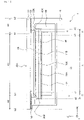
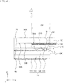
- FIG. 1 schematically illustrates a cross-sectional configuration of the display apparatus 1.
- the display apparatus 1 is, for example, a liquid crystal display apparatus used as a display monitor of a television, a notebook personal computer, or a car navigation system, for example, and includes a light guide member 40, a resin layer 20, a light shielding layer 50, and a transparent substrate 30, in this order, on front surface side (light emission side) of the display panel 10.
- a backlight unit 60 is provided on back side (light incident side) of the display panel 10.
- the display panel 10 and the backlight unit 60 are disposed in an exterior member 70.
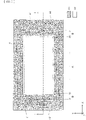
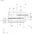
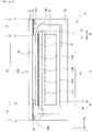
- FIG. 2 illustrates a planar configuration of the display apparatus 1 illustrated in FIG. 1 as viewed from side of the light shielding layer 50. In FIG. 2 , however, the transparent substrate 30 is omitted.
- FIG. 1 is a cross-sectional view in a direction of an arrow taken along a cutting line I-I illustrated in FIG. 2 .
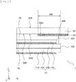
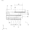
- FIG. 3 is an enlarged cross-sectional view of a main part of the display apparatus 1.
- the display panel 10 is a liquid crystal display panel that displays an image on the basis of illumination light from the backlight unit 60, and is of an active matrix type for displaying the image for each pixel on the basis of an image signal transmitted from a data driver (not illustrated) by means of a drive signal supplied from a gate driver (not illustrated).
- the display panel 10 includes pixels (not illustrated) that are arranged in 3,840 columns or more in an X direction and 2,160 rows or more in a Y direction, for example. Each pixel includes a red subpixel that emits red light, a green subpixel that emits green light, and a blue subpixel that emits blue light.
- the display panel 10 seals, between a drive substrate 10A and an opposite substrate 10B, an unillustrated liquid crystal layer.
- Film-like polarizing plates 11A and 11B as optical films, for example, are joined to external surfaces of the drive substrate 10A and the opposite substrate 10B, respectively.
- the drive substrate 10A includes a TFT (Thin Film Transistor) that drives each pixel, a drive circuit that supplies image signals and so forth to each pixel, and a wiring substrate for external coupling, which are disposed on a glass substrate, for example.
- the opposite substrate 10B includes respective color filters of unillustrated three primary colors (R, G, B) that are formed on a glass substrate for each pixel, for example.
- the liquid crystal layer to be used includes a nematic liquid crystal in a VA (Vertical Alignment) mode, in a TN (Twisted Nematic) mode, in an IPS (In Plane Switching) mode, for example.
- VA Vertical Alignment
- TN Transmission Nematic
- IPS In Plane Switching
- the drive substrate 10A and the opposite substrate 10B may not necessarily be provided in this order.
- the color filter may not particularly be provided.
- the color filter may be provided not on the opposite substrate 10B but on the drive substrate 10A.
- a periphery of a display region A (a rectangular region surrounded by an outer edge a1) serves as a peripheral region B (a frame-shaped region between the outer edge a1 and an outer edge a2 of the display panel 10).
- a plurality of pixels are disposed in matrix on the display region A, and the drive circuit for driving of each pixel, the wiring substrate for external coupling, and so forth as described above are disposed in the peripheral region B.
- the drive substrate 10A and the opposite substrate 10B are joined to each other in a portion of the peripheral region B along the outer edge a2 by means of an adhesive (not illustrated), for example.
- the resin layer 20 has a function of suppressing interface reflection between the display panel 10 and the transparent substrate 30, and is provided to improve resistance to impact.
- the resin layer 20 includes, for example, a resin based on silicone, epoxy, or acrylic, etc., that is cured by ultraviolet light or visible light (hereinbelow, photocurable resin), and preferably includes an acrylic-based resin.
- the acrylic-based resin include a resin composition that includes an oligomer, an acrylic monomer, a photopolymerization initiator, and a plasticizer.
- the oligomer include polyurethane acrylate, polyisoprene-based acrylate, polyester acrylate, and epoxy acrylate.
- the acrylic monomer include a monofunctional acrylic monomer such as isobornyl acrylate, benzyl acrylate, and 2-hydroxyethyl methacrylate.
- the resin layer 20 desirably covers also the outer edge of the polarizing plate 11B, as illustrated in FIG. 1 .
- One reason for this is that exposure of the polarizing plate 11B is prevented to sufficiently protect the polarizing plate 11B.
- the transparent substrate 30 is a so-called front panel that is disposed for the purpose of surface protection and design improvement of the display panel 10.
- the transparent substrate 30 has a thickness of, for example, about 0.2 mm to about 5.0 mm, and includes glass or plastic, for example. Examples of the plastic include acrylic and polycarbonate. Particularly for application of a large display, however, it is desirable to use a glass material in terms of dimensional stability.
- either a non-reflection treatment or a low-reflection treatment may be preferably performed on a surface on front surface side (observation side or light emission side) of the transparent substrate 30.
- An external dimension of the transparent substrate 30 is larger than the external dimension of the display panel 10, and an outer edge b2 of the transparent substrate 30 overhangs about 5 mm to about 100 mm, for example, outward from the outer edge a2 of the display panel 10.
- a rectangular region facing the display region A of the transparent substrate 30 serves as a translucent region R1 that transmits display light therethrough.
- the light shielding layer 50 is disposed in a frame-shaped light shielding region R2, on a back surface 30B of the transparent substrate 30, that faces the peripheral region B for the purpose of improvement in image quality and design.
- the back surface 30B is a surface, of the transparent substrate 30, that faces the display panel 10.
- the light shielding region R2 is a region that surrounds the translucent region R1 in an XY plane.
- the light shielding layer 50 has a thickness of, for example, about 0.1 ⁇ m to about 100 ⁇ m, and includes an opaque material such as carbon black, metal, pigment, and dye.
- An inner edge b1 of the light shielding layer 50 is preferably located outer than the outer edge a1 that is a boundary between the display region A and the peripheral region B of the display panel 10. This makes it possible to prevent pixels of the display panel 10 from being shielded by the light shielding layer 50 when observing the display apparatus 1 from a diagonal direction.
- the light guide member 40 includes an end surface 40K, and includes a plate-like transparent material.
- the light guide member 40 is inserted between, for example, the polarizing plate 11B of the display panel 10 and the resin layer 20.
- the light guide member 40 guides external light (such as ultraviolet light) from the end surface 40K and functions to effectively apply light to the photocurable resin that configures the resin layer 20.
- the light guide member 40 is disposed to occupy at least a portion of an overlapping region OR of the light shielding layer 50 and the display panel 10, out of the space interposed between the display panel 10 and the transparent substrate 30.
- the light guide member 40 is disposed to uniformly occupy also the translucent region R1 surrounded by the light shielding region R2 of the transparent substrate 30, where the light shielding layer 50 is provided.
- the backlight unit 60 illuminates the display panel 10 from its back surface directly or via an optical member such as a light guide plate, using, as a light source, a fluorescent lamp such as a CCFL (Cold Cathode Fluorescent Lamp), a light emitting diode (LED: Light Emitting Diode), or a laser (LASER: light amplification by stimulated emission of radiation), for example.
- a fluorescent lamp such as a CCFL (Cold Cathode Fluorescent Lamp), a light emitting diode (LED: Light Emitting Diode), or a laser (LASER: light amplification by stimulated emission of radiation
- the display apparatus 1 may be manufactured in the following manner, for example.
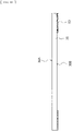
- FIGs. 4A to 4C illustrate a portion of the method of manufacturing the display apparatus 1 in the order of the process steps.
- the display panel 10 is fabricated as illustrated in FIG. 4A .
- the drive substrate 10A provided with the TFT, the drive circuit, and so forth is joined to the opposite substrate 10B including a color filter, with the liquid crystal layer being interposed therebetween.
- the polarizing plate 11A and the polarizing plate 11B are joined to external surfaces of the drive substrate 10A and the opposite substrate 10B, respectively.
- the light guide member 40 is placed on the polarizing plate 11B. In this situation, the polarizing plate 11B and the light guide member 40 may be fixed by means of adhesion, for example.
- the light shielding layer 50 is formed on a front surface 30A of the transparent substrate 30.
- the light shielding layer 50 is provided on the back surface 30B of the transparent substrate 30, by printing a predetermined opaque material dispersed or dissolved in a binder, or by directly vapor-depositing the opaque material, for example.
- a transparent film 51 on which the light shielding layer 50 is printed may be joined to the whole back surface 30B of the transparent substrate 30, for example.
- the non-reflection treatment or the low-reflection treatment may be preferably performed on the front surface 30A of the transparent substrate 30. It is possible for these treatments to be performed by, for example, vapor-depositing or coating a non-reflective material or a low-reflective material, or by joining a non-reflective film or a low-reflective film, for example.
- the display panel 10 including the light guide member 40 and the transparent substrate 30 including the light shielding layer 50 are overlapped, for example, via a resin 21 in a liquid state having photocurability.
- a portion of the light guide member 40 is made to overlap a portion of the light shielding layer 50. That is, a vicinity of the outer edge of the light guide member 40 is made to be included in the overlapping region OR (see FIG. 4D ).
- light L in a wavelength range that cures the resin 21, such as ultraviolet light and visible light is applied from both of the front surface 30A of the transparent substrate 30 and an end surface 21K of the resin 21.
- a lamp with its light emission center of 365 nm or 405 nm or an LED having such an emission wavelength may be preferably used, in terms of productivity.
- illuminance and light amount of the light L may be set depending on the composition and the thickness, for example, of the resin material used as the resin 21. It is desirable that the resin 21 be applied with a film thickness as uniform as possible by a method such as slit coating, roll coating, screen printing, and stencil printing. Curing the resin 21 by applying the light L in this manner allows for forming of the resin layer 20, resulting in joining of the display panel 10 and the transparent substrate 30 together.
- the display panel 10 and the transparent substrate 30 that are joined together are disposed in the exterior member 70 together with the backlight unit 60.
- the display apparatus 1 illustrated in FIG. 1 is completed as described above.
- the incident light passes through the polarizing plate 11A, and then is transmitted through the unillustrated liquid crystal layer while being modulated for each pixel, on the basis of an image voltage applied between the drive substrate 10A and the opposite substrate 10B.
- the light having been transmitted through the liquid crystal layer passes through the opposite substrate 10B including the color filter that is unillustrated, whereby the transmitted light is extracted to the outside of the polarizing plate 11B as color display light.
- the light shielding layer 50 is disposed on the back surface 30B, of the transparent substrate 30, that faces the display panel 10. Therefore, even when a foreign matter D is mixed into the light shielding layer 50, the foreign matter is less likely to be visually recognized upon being viewed by an observer from the front surface 30A of the transparent substrate 30 (see FIG. 4D ). In more detail, the foreign matter D is more likely to be visually recognized by the observer in a case where the foreign matter D is exposed on a front surface 50A (a surface that faces the back surface 30B) of the light shielding layer 50.
- the display apparatus 1 makes it possible to achieve a structure suitable for improvement in production yield.
- the light shielding layer 50 is formed on the front surface 30A of the transparent substrate 30. Therefore, the foreign matter D is more likely to be visually recognized no matter where in the light shielding layer 50 the foreign matter D is present, upon being viewed by the observer from the front surface 30A of the transparent substrate 30.
- the photocurable resin 21 is filled between the transparent substrate 30 and the display panel 10, and is cured by applying light having a predetermined wavelength (light L) to the resin 21.
- light L a predetermined wavelength
- the light shielding layer 50 is provided on the back surface 30B of the transparent substrate 30
- quick curing of the resin 21 may be prevented when the light L is applied only from the front surface 30A of the transparent substrate 30.
- a portion of the light L is prevented from reaching the resin 21 by being shielded by the light shielding layer 50. Therefore, a method of causing the light L to be incident also from the end surface 21K of the resin 21 is employed.
- the display apparatus 1 has a configuration in which the light guide member 40 is provided to occupy at least a portion of the overlapping region OR of the light shielding layer 50 and the display panel 10.
- the light guide member 40 allows the light L having been incident from the end surface 21K to propagate in the XY plane, whereby the light L with sufficient intensity is applied to the resin 21 that occupies the overlapping region OR (resin 21 in a circle 21R illustrated in FIG. 4D ).
- curing of the resin 21 is promoted to prevent its non-curing, thereby allowing for formation of the resin layer 20 having substantially uniform optical properties.
- FIG. 5 illustrates a cross-sectional configuration of a main part of a display apparatus 1A according to a first modification example of the foregoing first embodiment.
- the display apparatus 1A has a configuration similar to that of the display apparatus 1 except that the end surface 40K of the light guide member 40 is exposed without being covered by the resin layer 20. It is to be noted that, although FIG. 5 illustrates an example in which the location of the end surface 40K coincides with the location of an end surface 20K of the resin layer 20, their locations may be different.
- the display apparatus 1A has a configuration in which the end surface 40K of the light guide member 40 is exposed without being covered by the resin layer 20, thus making it possible to cure the resin 21 more efficiently when joining the display panel 10 and the transparent substrate 30 together through formation of the resin layer 20. That is, the display apparatus 1A enables the light L that promotes curing of the resin 21 to propagate inside the light guide member 40 from the end surface 40K toward the display region A without being blocked by the resin layer 20. Therefore, as compared with the display apparatus 1 with the end surface 40K being covered by the resin layer 20, the display apparatus 1A enables more intense light to be applied to the resin 21 that occupies the overlapping region OR while suppressing reduction in intensity of the light L.
- FIG. 6A illustrates a cross-sectional configuration of a main part of a display apparatus 1B according to a second modification example of the foregoing first embodiment.
- the display apparatus 1B has a configuration similar to that of the display apparatus 1 except that the display apparatus 1B includes a light guide member 41 instead of the light guide member 40.
- the light guide member 40 is a plate member having a rectangular planar shape, and covers also the polarizing plate 11B in the display region A.
- the light guide member 41 is provided only in the overlapping region OR. That is, as illustrated in FIG.
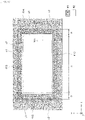
- the display apparatus 1B has a frame-shaped planar shape that extends to overlap the light shielding layer 50. It is to be noted that FIG. 6B illustrates the planar configuration of the display apparatus 1B illustrated in FIG. 5A as viewed from side of the light shielding layer 50. In FIG. 6B , however, the transparent substrate 30 is omitted.
- FIG. 6A is a cross-sectional view in a direction of an arrow taken along a cutting line VIA-VIA illustrated in FIG. 6B . It is to be noted that, as illustrated in FIG. 6C as another modification example (third modification example), a plurality of light guide members 41A to 41D may be discretely disposed instead of the light guide member 41 having a frame shape.
- the display apparatus 1B has a configuration in which the light guide member 41 is disposed in the overlapping region OR, thus allowing the light L with sufficient intensity to be also applied to the resin 21 that occupies the overlapping region OR when forming the resin layer 20 adjacent to the light guide member 41, making it possible to prevent non-curing of the resin 21. Meanwhile, the light guide member 41 is not present in regions other than the overlapping region OR, thus making it possible to reduce the weight as compared with the above-described display apparatuses 1 and 1A.
- FIG. 7 illustrates a cross-sectional configuration of a main part of a display apparatus 2 according to a second embodiment of the technology.
- the light guide member 40 is provided between the display panel 10 and the resin layer 20.
- the display apparatus 2 has a configuration in which the light guide member 40 is provided to be in contact with the rear surface 50B of the light shielding layer 50 provided on the back surface 30B of the transparent substrate 30 (between the transparent substrate 30 and the resin layer 20).
- the transparent substrate 30, the light shielding layer 50, and the light guide member 40 configure a transparent plate unit.
- the light guide member 40 is disposed to face the transparent substrate 30, with the light shielding layer 50 being interposed therebetween.
- a space surrounded by the transparent substrate 30, the light shielding layer 50, and the light guide member 40 may include a transparent material layer or an air layer.
- the display apparatus 2 has a configuration similar to that of the display apparatus 1 except that a location in which the light guide member 40 is disposed is different from that in the display apparatus 1.
- the display apparatus 2 has a configuration in which the light shielding layer 50 is provided on the back surface 30B of the transparent substrate 30, thus allowing for expectation of improvement in production yield, as with the display apparatus 1. Moreover, the display apparatus 2 has a configuration in which the light guide member 40 is provided to be in contact with the rear surface 50B of the light shielding layer 50, thus making it possible to promote curing of the resin 21 when forming the resin layer 20, regardless of the configuration of the display panel 10.
- One reason for this is that propagation of the light L inside the light guide member 40 is less likely to be blocked due to the light guide member 40 being spaced apart from the display panel 10.
- provision of the light guide member 40 at a location spaced apart from the display panel 10 allows for reduction in distortion, for example, caused by mechanical load on the display panel 10, as compared with a case where the light guide member 40 is joined to the display panel 10. This makes it possible to eliminate a cause of degradation in display quality of the display panel 10.
- the end surface 40K of the light guide member 40 may be exposed without being covered by the resin layer 20, as in a display apparatus 2A according to a first modification example illustrated in FIG. 8 , for example.
- the location of the end surface 40K either may coincide with or may differ from the location of the end surface 20K of the resin layer 20.
- the light guide member 41 having a frame shape may be provided only in the overlapping region OR instead of the light guide member 40, as in a display apparatus 2B according to a second modification example illustrated in FIG. 9 , for example.
- the light guide member 41 having the frame shape may be divided into a plurality of pieces to be disposed.
- the disclosure is not limited to the foregoing embodiments, etc., and may be modified in a variety of ways.
- the materials and the thicknesses of the respective layers described in the foregoing embodiments, etc. are not limitative; other materials and thicknesses may also be employed.
- the disclosure is also applicable to a case of using another type of the display panel 10 such as an organic EL (Electroluminescence) panel and a plasma display panel.
- an organic EL (Electroluminescence) panel and a plasma display panel.
- it is possible to avoid degradation of image quality due to non-curing of the resin layer 20.
- the light guide member is a planar or frame-shaped transparent member having a homogeneous optical action
- the disclosure is not limited thereto.
- an optical device that exhibits an optical function such as a pattern retarder, a lenticular lens, a liquid crystal layer barrier, and a parallax barrier may be used as the light guide member.
- the display apparatus including both such a light guide member and a display panel that displays a plurality of viewpoint images is usable as a stereoscopic display apparatus having a stereoscopic display function, as a result of the light guide member exhibiting, for example, a function of optically separating the plurality of viewpoint images displayed on the display panel to allow for stereoscopic vision.
- an optical device that has various optical functions such as a touch panel, a light diffusion sheet having a function of increasing a viewing angle, a prism sheet or lens sheet having a light condensing function, and an anti-reflection sheet may also be used as the light guide member. Furthermore, a combination of two or more of these optical devices that have respective optical functions may also be used.
- the foregoing embodiments, etc. are described by exemplifying a case where the light guide member 40 or 41 is in contact with the polarizing plate 11B or the light shielding layer 50, the disclosure is not limited thereto.
- the light guide member 40 may be embedded in the resin layer 20, and a periphery of the light guide member 40 may be surrounded by the resin layer 20, as in a display apparatus 3 according to another modification example illustrated in FIG. 10 .
Landscapes
- Physics & Mathematics (AREA)
- Nonlinear Science (AREA)
- General Physics & Mathematics (AREA)
- Optics & Photonics (AREA)
- Crystallography & Structural Chemistry (AREA)
- Chemical & Material Sciences (AREA)
- Mathematical Physics (AREA)
- Engineering & Computer Science (AREA)
- Multimedia (AREA)
- Signal Processing (AREA)
- Theoretical Computer Science (AREA)
- Devices For Indicating Variable Information By Combining Individual Elements (AREA)
- Liquid Crystal (AREA)
- Illuminated Signs And Luminous Advertising (AREA)
Description
- The disclosure relates to a display apparatus such as a television, and to a display unit and a transparent plate unit each used in the display unit.
- Recently, for example, a display apparatus such as a liquid crystal or organic EL (Electroluminescence) type is used as a display monitor of a flat screen television, a notebook personal computer, or a car navigation system, for example. It is known, in terms of surface protection and design, that such a display apparatus may include a front panel configured by a transparent substrate of plastic or glass, for example, provided on front side (display side) of the display panel (for example, see
PTLs 1 to 6). - In some cases, the front panel used in this example may be subjected to a light shielding treatment (a light shielding layer may be formed) in a region facing a non-display part (bezel part) in terms of image quality improvement and design. Specifically, the light shielding layer is formed in a frame-shaped region along a periphery of the front panel by, for example, vapor deposition or printing of a light-shielding material or by joining of an opaque sheet material. In some cases, a resin layer is provided between the display unit and the transparent plate (see
PTL 7, 8). In some cases, a touch panel or 3D filter may be bonded to the resin layer (see PTL 9). -
- PTL 1:
Japanese Unexamined Patent Application Publication No. H03-204616 - PTL 2:
Japanese Unexamined Patent Application Publication No. H06-337411 - PTL 3:
Japanese Unexamined Patent Application Publication No. 2005-55641 - PTL 4:
Japanese Unexamined Patent Application Publication No. 2008-281997 - PTL 5:
Japanese Unexamined Patent Application Publication No. 2012-113228 - PTL 6:
Japanese Unexamined Patent Application Publication No. 2014-235185 - PTL 7:
Japanese Patent Publication No. 2008-281997 - PTL 8:
US Patent Application Publication No. 2010-0043965 - PTL 9:
US Patent Application Publication No. 2013-0011597 - Incidentally, when a foreign matter is mixed into a light shielding layer of a front panel as described above, it is often visually recognized by an observer.
- It is thus desirable to provide a display apparatus having a structure suitable for improvement in production yield, and a display unit and a transparent plate unit each used in the display apparatus.
- A display apparatus according to the invention is as recited in
independent claim 1 anddependent claims 2 to 12. Furthermore, a method of manufacturing the display apparatus ofclaims 1 to 12 is as recited in claims 13 to 15. - According to the display apparatus of the respective embodiments of the invention, it is possible to achieve a structure suitable for improvement in production yield.
-
- [
FIG. 1] FIG. 1 is a cross-sectional view of a configuration of a display apparatus according to a first embodiment of the disclosure. - [
FIG. 2] FIG. 2 is a plan view of the configuration of the display apparatus illustrated inFIG. 1 as viewed from a light shielding layer. - [
FIG. 3] FIG. 3 is an enlarged cross-sectional view of a main part of the display apparatus illustrated inFIG. 1 . - [
FIG. 4A] FIG. 4A is a cross-sectional view of one process step of a method of manufacturing the display apparatus illustrated inFIG. 1 . - [
FIG. 4B] FIG. 4B is a cross-sectional view of one process step subsequent toFIG. 4A - [
FIG. 4C] FIG. 4C is a cross-sectional view of one process step subsequent toFIG. 4B . - [
FIG. 4D] FIG. 4D is an enlarged cross-sectional view of the process step illustrated inFIG. 4C . - [
FIG. 5] FIG. 5 is a cross-sectional view of a first modification example of the display apparatus illustrated inFIG. 1 . - [
FIG. 6A] FIG. 6A is a cross-sectional view of a second modification example of the display apparatus illustrated inFIG. 1 . - [
FIG. 6B] FIG. 6B is a plan view of the second modification example of the display apparatus illustrated inFIG. 1 . - [
FIG. 6C] FIG. 6C is a plan view of a third modification example of the display apparatus illustrated inFIG. 1 . - [
FIG. 7] FIG. 7 is a cross-sectional view of a configuration of a display apparatus according to a second embodiment of the disclosure. - [
FIG. 8] FIG. 8 is a cross-sectional view of a first modification example of the display apparatus illustrated inFIG. 7 . - [
FIG. 9] FIG. 9 is a cross-sectional view of a second modification example of the display apparatus illustrated inFIG. 7 . - [
FIG. 10] FIG. 10 is a cross-sectional view of the display apparatus according to another modification example of the disclosure. - [
FIG. 11] FIG. 11 is an enlarged cross-sectional view of a main part of a display apparatus according to a comparative example. - In the following, some embodiments of the disclosure are described in detail with reference to the drawings. The description is given in the following order. It is to be noted that the disclosure is not limited to the following examples and that a known configuration may also be added thereto where appropriate.
- 1. First Embodiment:
An example of a display apparatus including a display unit provided with a light guide member on a display panel. - 2. First Modification Example of First Embodiment:
An example in which an end surface of the light guide member is exposed to the outside. - 3. Second and Third Modification Examples of First Embodiment:
Examples of a display apparatus provided with a frame-shaped light guide member. - 4. Second Embodiment and Modification Example Thereof:
Examples of a display apparatus including a transparent plate unit provided with the light guide member on a transparent substrate. - 5. Other Modification Examples
- A configuration of a
display apparatus 1 according to a first embodiment of the disclosure is described with reference toFIGs. 1 to 3 .FIG. 1 schematically illustrates a cross-sectional configuration of thedisplay apparatus 1. Thedisplay apparatus 1 is, for example, a liquid crystal display apparatus used as a display monitor of a television, a notebook personal computer, or a car navigation system, for example, and includes alight guide member 40, aresin layer 20, alight shielding layer 50, and atransparent substrate 30, in this order, on front surface side (light emission side) of thedisplay panel 10. Abacklight unit 60 is provided on back side (light incident side) of thedisplay panel 10. Thedisplay panel 10 and thebacklight unit 60 are disposed in anexterior member 70. Moreover, thedisplay panel 10 configures a display unit together with thelight guide member 40.FIG. 2 illustrates a planar configuration of thedisplay apparatus 1 illustrated inFIG. 1 as viewed from side of thelight shielding layer 50. InFIG. 2 , however, thetransparent substrate 30 is omitted.FIG. 1 is a cross-sectional view in a direction of an arrow taken along a cutting line I-I illustrated inFIG. 2 .FIG. 3 is an enlarged cross-sectional view of a main part of thedisplay apparatus 1. - The
display panel 10 is a liquid crystal display panel that displays an image on the basis of illumination light from thebacklight unit 60, and is of an active matrix type for displaying the image for each pixel on the basis of an image signal transmitted from a data driver (not illustrated) by means of a drive signal supplied from a gate driver (not illustrated). Thedisplay panel 10 includes pixels (not illustrated) that are arranged in 3,840 columns or more in an X direction and 2,160 rows or more in a Y direction, for example. Each pixel includes a red subpixel that emits red light, a green subpixel that emits green light, and a blue subpixel that emits blue light. Thedisplay panel 10 seals, between adrive substrate 10A and anopposite substrate 10B, an unillustrated liquid crystal layer. Film-likepolarizing plates drive substrate 10A and theopposite substrate 10B, respectively. Thedrive substrate 10A includes a TFT (Thin Film Transistor) that drives each pixel, a drive circuit that supplies image signals and so forth to each pixel, and a wiring substrate for external coupling, which are disposed on a glass substrate, for example. Theopposite substrate 10B includes respective color filters of unillustrated three primary colors (R, G, B) that are formed on a glass substrate for each pixel, for example. The liquid crystal layer to be used includes a nematic liquid crystal in a VA (Vertical Alignment) mode, in a TN (Twisted Nematic) mode, in an IPS (In Plane Switching) mode, for example. It is to be noted that thedrive substrate 10A and theopposite substrate 10B may not necessarily be provided in this order. Moreover, the color filter may not particularly be provided. Alternatively, the color filter may be provided not on theopposite substrate 10B but on thedrive substrate 10A. Furthermore, it is also possible to use a driving element other than the TFT. - As illustrated in
FIG. 2 , in thedisplay panel 10, a periphery of a display region A (a rectangular region surrounded by an outer edge a1) serves as a peripheral region B (a frame-shaped region between the outer edge a1 and an outer edge a2 of the display panel 10). A plurality of pixels are disposed in matrix on the display region A, and the drive circuit for driving of each pixel, the wiring substrate for external coupling, and so forth as described above are disposed in the peripheral region B. Thedrive substrate 10A and theopposite substrate 10B are joined to each other in a portion of the peripheral region B along the outer edge a2 by means of an adhesive (not illustrated), for example. - The
resin layer 20 has a function of suppressing interface reflection between thedisplay panel 10 and thetransparent substrate 30, and is provided to improve resistance to impact. Theresin layer 20 includes, for example, a resin based on silicone, epoxy, or acrylic, etc., that is cured by ultraviolet light or visible light (hereinbelow, photocurable resin), and preferably includes an acrylic-based resin. Preferable examples of the acrylic-based resin include a resin composition that includes an oligomer, an acrylic monomer, a photopolymerization initiator, and a plasticizer. Examples of the oligomer include polyurethane acrylate, polyisoprene-based acrylate, polyester acrylate, and epoxy acrylate. Preferable examples of the acrylic monomer include a monofunctional acrylic monomer such as isobornyl acrylate, benzyl acrylate, and 2-hydroxyethyl methacrylate. It is to be noted that theresin layer 20 desirably covers also the outer edge of thepolarizing plate 11B, as illustrated inFIG. 1 . One reason for this is that exposure of thepolarizing plate 11B is prevented to sufficiently protect thepolarizing plate 11B. - The
transparent substrate 30 is a so-called front panel that is disposed for the purpose of surface protection and design improvement of thedisplay panel 10. Thetransparent substrate 30 has a thickness of, for example, about 0.2 mm to about 5.0 mm, and includes glass or plastic, for example. Examples of the plastic include acrylic and polycarbonate. Particularly for application of a large display, however, it is desirable to use a glass material in terms of dimensional stability. Moreover, either a non-reflection treatment or a low-reflection treatment may be preferably performed on a surface on front surface side (observation side or light emission side) of thetransparent substrate 30. - An external dimension of the
transparent substrate 30 is larger than the external dimension of thedisplay panel 10, and an outer edge b2 of thetransparent substrate 30 overhangs about 5 mm to about 100 mm, for example, outward from the outer edge a2 of thedisplay panel 10. A rectangular region facing the display region A of thetransparent substrate 30 serves as a translucent region R1 that transmits display light therethrough. - The
light shielding layer 50 is disposed in a frame-shaped light shielding region R2, on aback surface 30B of thetransparent substrate 30, that faces the peripheral region B for the purpose of improvement in image quality and design. Theback surface 30B is a surface, of thetransparent substrate 30, that faces thedisplay panel 10. The light shielding region R2 is a region that surrounds the translucent region R1 in an XY plane. Thelight shielding layer 50 has a thickness of, for example, about 0.1 µm to about 100 µm, and includes an opaque material such as carbon black, metal, pigment, and dye. An inner edge b1 of thelight shielding layer 50 is preferably located outer than the outer edge a1 that is a boundary between the display region A and the peripheral region B of thedisplay panel 10. This makes it possible to prevent pixels of thedisplay panel 10 from being shielded by thelight shielding layer 50 when observing thedisplay apparatus 1 from a diagonal direction. - The
light guide member 40 includes anend surface 40K, and includes a plate-like transparent material. Thelight guide member 40 is inserted between, for example, thepolarizing plate 11B of thedisplay panel 10 and theresin layer 20. When thedisplay panel 10 and thetransparent substrate 30 are joined together, thelight guide member 40 guides external light (such as ultraviolet light) from theend surface 40K and functions to effectively apply light to the photocurable resin that configures theresin layer 20. Thelight guide member 40 is disposed to occupy at least a portion of an overlapping region OR of thelight shielding layer 50 and thedisplay panel 10, out of the space interposed between thedisplay panel 10 and thetransparent substrate 30. - Moreover, in the example illustrated in
FIG. 1 , thelight guide member 40 is disposed to uniformly occupy also the translucent region R1 surrounded by the light shielding region R2 of thetransparent substrate 30, where thelight shielding layer 50 is provided. - The
backlight unit 60 illuminates thedisplay panel 10 from its back surface directly or via an optical member such as a light guide plate, using, as a light source, a fluorescent lamp such as a CCFL (Cold Cathode Fluorescent Lamp), a light emitting diode (LED: Light Emitting Diode), or a laser (LASER: light amplification by stimulated emission of radiation), for example. - The
display apparatus 1 may be manufactured in the following manner, for example.FIGs. 4A to 4C illustrate a portion of the method of manufacturing thedisplay apparatus 1 in the order of the process steps. - First, the
display panel 10 is fabricated as illustrated inFIG. 4A . Specifically, thedrive substrate 10A provided with the TFT, the drive circuit, and so forth is joined to theopposite substrate 10B including a color filter, with the liquid crystal layer being interposed therebetween. Thereafter, thepolarizing plate 11A and thepolarizing plate 11B are joined to external surfaces of thedrive substrate 10A and theopposite substrate 10B, respectively. Furthermore, thelight guide member 40 is placed on thepolarizing plate 11B. In this situation, thepolarizing plate 11B and thelight guide member 40 may be fixed by means of adhesion, for example. - Meanwhile, as illustrated in
FIG. 4B , thelight shielding layer 50 is formed on afront surface 30A of thetransparent substrate 30. Specifically, thelight shielding layer 50 is provided on theback surface 30B of thetransparent substrate 30, by printing a predetermined opaque material dispersed or dissolved in a binder, or by directly vapor-depositing the opaque material, for example. Alternately, a transparent film 51 on which thelight shielding layer 50 is printed may be joined to thewhole back surface 30B of thetransparent substrate 30, for example. - It is to be noted that the non-reflection treatment or the low-reflection treatment may be preferably performed on the
front surface 30A of thetransparent substrate 30. It is possible for these treatments to be performed by, for example, vapor-depositing or coating a non-reflective material or a low-reflective material, or by joining a non-reflective film or a low-reflective film, for example. - Subsequently, as illustrated in
FIGs. 4C and4D , thedisplay panel 10 including thelight guide member 40 and thetransparent substrate 30 including thelight shielding layer 50 are overlapped, for example, via aresin 21 in a liquid state having photocurability. In this situation, a portion of thelight guide member 40 is made to overlap a portion of thelight shielding layer 50. That is, a vicinity of the outer edge of thelight guide member 40 is made to be included in the overlapping region OR (seeFIG. 4D ). Thereafter, light L in a wavelength range that cures theresin 21, such as ultraviolet light and visible light, is applied from both of thefront surface 30A of thetransparent substrate 30 and anend surface 21K of theresin 21. Specifically, it suffices to use light having a wavelength to which a photoinitiator in theresin 21 is sensitive. It is to be noted that, for example, a lamp with its light emission center of 365 nm or 405 nm or an LED having such an emission wavelength may be preferably used, in terms of productivity. Moreover, illuminance and light amount of the light L may be set depending on the composition and the thickness, for example, of the resin material used as theresin 21. It is desirable that theresin 21 be applied with a film thickness as uniform as possible by a method such as slit coating, roll coating, screen printing, and stencil printing. Curing theresin 21 by applying the light L in this manner allows for forming of theresin layer 20, resulting in joining of thedisplay panel 10 and thetransparent substrate 30 together. - After thus joining the
transparent substrate 30 to thedisplay panel 10, with theresin layer 20 being interposed therebetween, thedisplay panel 10 and thetransparent substrate 30 that are joined together are disposed in theexterior member 70 together with thebacklight unit 60. Thedisplay apparatus 1 illustrated inFIG. 1 is completed as described above. - In the
display apparatus 1, when light enters thedisplay panel 10 from thebacklight unit 60, the incident light passes through thepolarizing plate 11A, and then is transmitted through the unillustrated liquid crystal layer while being modulated for each pixel, on the basis of an image voltage applied between thedrive substrate 10A and theopposite substrate 10B. The light having been transmitted through the liquid crystal layer passes through theopposite substrate 10B including the color filter that is unillustrated, whereby the transmitted light is extracted to the outside of thepolarizing plate 11B as color display light. - In the
display apparatus 1, thelight shielding layer 50 is disposed on theback surface 30B, of thetransparent substrate 30, that faces thedisplay panel 10. Therefore, even when a foreign matter D is mixed into thelight shielding layer 50, the foreign matter is less likely to be visually recognized upon being viewed by an observer from thefront surface 30A of the transparent substrate 30 (seeFIG. 4D ). In more detail, the foreign matter D is more likely to be visually recognized by the observer in a case where the foreign matter D is exposed on afront surface 50A (a surface that faces theback surface 30B) of thelight shielding layer 50. In other cases such as a case where the foreign matter D is exposed to arear surface 50B and a case where the foreign matter D is embedded in thelight shielding layer 50, however, the foreign matter D is less likely to be visually recognized by the observer. Accordingly, thedisplay apparatus 1 makes it possible to achieve a structure suitable for improvement in production yield. - In contrast, in a
display apparatus 101 illustrated inFIG. 11 as a comparative example, thelight shielding layer 50 is formed on thefront surface 30A of thetransparent substrate 30. Therefore, the foreign matter D is more likely to be visually recognized no matter where in thelight shielding layer 50 the foreign matter D is present, upon being viewed by the observer from thefront surface 30A of thetransparent substrate 30. - Moreover, when joining the
transparent substrate 30 and thedisplay panel 10 together, thephotocurable resin 21 is filled between thetransparent substrate 30 and thedisplay panel 10, and is cured by applying light having a predetermined wavelength (light L) to theresin 21. Here, in a case where thelight shielding layer 50 is provided on theback surface 30B of thetransparent substrate 30, there is a possibility that quick curing of theresin 21 may be prevented when the light L is applied only from thefront surface 30A of thetransparent substrate 30. One reason for this is that a portion of the light L is prevented from reaching theresin 21 by being shielded by thelight shielding layer 50. Therefore, a method of causing the light L to be incident also from theend surface 21K of theresin 21 is employed. In a case where theresin 21 is relatively thin, however, there is a possibility that the light L having been incident from theend surface 21K may not reach theresin 21 near the inner edge b1 of thelight shielding layer 50, or that intensity of the light L may be insufficient even when the light L reaches there. In such a case, curing of theresin 21 may be insufficient near the inner edge b1 of thelight shielding layer 50, which may cause occurrence of display unevenness. - Thus, the
display apparatus 1 according to the present embodiment has a configuration in which thelight guide member 40 is provided to occupy at least a portion of the overlapping region OR of thelight shielding layer 50 and thedisplay panel 10. Thelight guide member 40 allows the light L having been incident from theend surface 21K to propagate in the XY plane, whereby the light L with sufficient intensity is applied to theresin 21 that occupies the overlapping region OR (resin 21 in acircle 21R illustrated inFIG. 4D ). As a result, curing of theresin 21 is promoted to prevent its non-curing, thereby allowing for formation of theresin layer 20 having substantially uniform optical properties. Thus, it becomes possible to eliminate occurrence of the display unevenness. -
FIG. 5 illustrates a cross-sectional configuration of a main part of adisplay apparatus 1A according to a first modification example of the foregoing first embodiment. Thedisplay apparatus 1A has a configuration similar to that of thedisplay apparatus 1 except that theend surface 40K of thelight guide member 40 is exposed without being covered by theresin layer 20. It is to be noted that, althoughFIG. 5 illustrates an example in which the location of theend surface 40K coincides with the location of anend surface 20K of theresin layer 20, their locations may be different. - As described above, the
display apparatus 1A has a configuration in which theend surface 40K of thelight guide member 40 is exposed without being covered by theresin layer 20, thus making it possible to cure theresin 21 more efficiently when joining thedisplay panel 10 and thetransparent substrate 30 together through formation of theresin layer 20. That is, thedisplay apparatus 1A enables the light L that promotes curing of theresin 21 to propagate inside thelight guide member 40 from theend surface 40K toward the display region A without being blocked by theresin layer 20. Therefore, as compared with thedisplay apparatus 1 with theend surface 40K being covered by theresin layer 20, thedisplay apparatus 1A enables more intense light to be applied to theresin 21 that occupies the overlapping region OR while suppressing reduction in intensity of the light L. -
FIG. 6A illustrates a cross-sectional configuration of a main part of adisplay apparatus 1B according to a second modification example of the foregoing first embodiment. Thedisplay apparatus 1B has a configuration similar to that of thedisplay apparatus 1 except that thedisplay apparatus 1B includes alight guide member 41 instead of thelight guide member 40. In thedisplay apparatus 1 according to the foregoing first embodiment, thelight guide member 40 is a plate member having a rectangular planar shape, and covers also thepolarizing plate 11B in the display region A. In contrast, in thedisplay apparatus 1B, thelight guide member 41 is provided only in the overlapping region OR. That is, as illustrated inFIG. 6B , for example, thedisplay apparatus 1B has a frame-shaped planar shape that extends to overlap thelight shielding layer 50. It is to be noted thatFIG. 6B illustrates the planar configuration of thedisplay apparatus 1B illustrated in FIG. 5A as viewed from side of thelight shielding layer 50. InFIG. 6B , however, thetransparent substrate 30 is omitted.FIG. 6A is a cross-sectional view in a direction of an arrow taken along a cutting line VIA-VIA illustrated inFIG. 6B . It is to be noted that, as illustrated inFIG. 6C as another modification example (third modification example), a plurality oflight guide members 41A to 41D may be discretely disposed instead of thelight guide member 41 having a frame shape. - As described above, the
display apparatus 1B has a configuration in which thelight guide member 41 is disposed in the overlapping region OR, thus allowing the light L with sufficient intensity to be also applied to theresin 21 that occupies the overlapping region OR when forming theresin layer 20 adjacent to thelight guide member 41, making it possible to prevent non-curing of theresin 21. Meanwhile, thelight guide member 41 is not present in regions other than the overlapping region OR, thus making it possible to reduce the weight as compared with the above-describeddisplay apparatuses -
FIG. 7 illustrates a cross-sectional configuration of a main part of adisplay apparatus 2 according to a second embodiment of the technology. In thedisplay apparatus 1 according to the foregoing first embodiment and thedisplay apparatuses light guide member 40 is provided between thedisplay panel 10 and theresin layer 20. In contrast, thedisplay apparatus 2 has a configuration in which thelight guide member 40 is provided to be in contact with therear surface 50B of thelight shielding layer 50 provided on theback surface 30B of the transparent substrate 30 (between thetransparent substrate 30 and the resin layer 20). In thedisplay apparatus 2, thetransparent substrate 30, thelight shielding layer 50, and thelight guide member 40 configure a transparent plate unit. Thelight guide member 40 is disposed to face thetransparent substrate 30, with thelight shielding layer 50 being interposed therebetween. A space surrounded by thetransparent substrate 30, thelight shielding layer 50, and thelight guide member 40 may include a transparent material layer or an air layer. Thedisplay apparatus 2 has a configuration similar to that of thedisplay apparatus 1 except that a location in which thelight guide member 40 is disposed is different from that in thedisplay apparatus 1. - The
display apparatus 2 according to the present embodiment has a configuration in which thelight shielding layer 50 is provided on theback surface 30B of thetransparent substrate 30, thus allowing for expectation of improvement in production yield, as with thedisplay apparatus 1. Moreover, thedisplay apparatus 2 has a configuration in which thelight guide member 40 is provided to be in contact with therear surface 50B of thelight shielding layer 50, thus making it possible to promote curing of theresin 21 when forming theresin layer 20, regardless of the configuration of thedisplay panel 10. One reason for this is that propagation of the light L inside thelight guide member 40 is less likely to be blocked due to thelight guide member 40 being spaced apart from thedisplay panel 10. Moreover, provision of thelight guide member 40 at a location spaced apart from thedisplay panel 10 allows for reduction in distortion, for example, caused by mechanical load on thedisplay panel 10, as compared with a case where thelight guide member 40 is joined to thedisplay panel 10. This makes it possible to eliminate a cause of degradation in display quality of thedisplay panel 10. - In the present embodiment as well, the
end surface 40K of thelight guide member 40 may be exposed without being covered by theresin layer 20, as in adisplay apparatus 2A according to a first modification example illustrated inFIG. 8 , for example. In such a case, the location of theend surface 40K either may coincide with or may differ from the location of theend surface 20K of theresin layer 20. - Moreover, the
light guide member 41 having a frame shape may be provided only in the overlapping region OR instead of thelight guide member 40, as in adisplay apparatus 2B according to a second modification example illustrated inFIG. 9 , for example. In such a case, thelight guide member 41 having the frame shape may be divided into a plurality of pieces to be disposed. - Although description has been described above with reference to some embodiments and their modification examples, the disclosure is not limited to the foregoing embodiments, etc., and may be modified in a variety of ways. For example, the materials and the thicknesses of the respective layers described in the foregoing embodiments, etc. are not limitative; other materials and thicknesses may also be employed.
- Moreover, although the foregoing embodiments, etc. are described by exemplifying a case of using the liquid crystal display panel as the
display panel 10, the disclosure is also applicable to a case of using another type of thedisplay panel 10 such as an organic EL (Electroluminescence) panel and a plasma display panel. In a case where such a different type of the display panel is used, it is possible to avoid degradation of image quality due to non-curing of theresin layer 20. - Moreover, although the foregoing embodiments, etc. are described by exemplifying a case where the light guide member is a planar or frame-shaped transparent member having a homogeneous optical action, the disclosure is not limited thereto. For example, an optical device that exhibits an optical function such as a pattern retarder, a lenticular lens, a liquid crystal layer barrier, and a parallax barrier may be used as the light guide member. The display apparatus including both such a light guide member and a display panel that displays a plurality of viewpoint images is usable as a stereoscopic display apparatus having a stereoscopic display function, as a result of the light guide member exhibiting, for example, a function of optically separating the plurality of viewpoint images displayed on the display panel to allow for stereoscopic vision.
- Moreover, an optical device that has various optical functions such as a touch panel, a light diffusion sheet having a function of increasing a viewing angle, a prism sheet or lens sheet having a light condensing function, and an anti-reflection sheet may also be used as the light guide member. Furthermore, a combination of two or more of these optical devices that have respective optical functions may also be used.
- Moreover, although the foregoing embodiments, etc. are described by exemplifying a case where the
light guide member polarizing plate 11B or thelight shielding layer 50, the disclosure is not limited thereto. For example, thelight guide member 40 may be embedded in theresin layer 20, and a periphery of thelight guide member 40 may be surrounded by theresin layer 20, as in adisplay apparatus 3 according to another modification example illustrated inFIG. 10 . - It should be understood by those skilled in the art that various modifications, combinations, sub-combinations and alterations may occur depending on design requirements and other factors insofar as they are within the scope of the appended claims.
Claims (15)
- A display apparatus (1), comprising:a display panel (10) having a display region (A);a transparent plate (30) including an opposite surface (30B) that faces the display panel (10);a light shielding layer (50) provided in a peripheral part of the opposite surface (30B) of the transparent plate (30) so as to surround the display region (A);a resin layer (20) provided between the display panel (10) and the transparent plate (30) so as to cover the display region (A) and to extend into the overlapping region of the display panel (10) and the light shielding layer (50), characterized in that the display apparatus (1) further comprisesa light guide member (40) provided to occupy at least a portion of the overlapping region (OR) of the light shielding layer (50) and the display panel (10) out of a space interposed between the display panel (10) and the transparent plate (30), the light guide member (40) being configured to propagate the light having been used to photocure the resin layer (20).
- The display apparatus (1) according to claim 1, wherein the light guide member (40) is provided between the display panel (10) and the resin layer (20), provided between the transparent plate (30) and the resin layer (20), or embedded in the resin layer (20).
- The display apparatus (1) according to claim 1, wherein the light guide member (40) includes a part that is not covered by the resin layer (20).
- The display apparatus (1) according to claim 1, wherein the light guide member (40) is provided to occupy also a central region surrounded by a light shielding region (R2) occupied by the light shielding layer (50) in the transparent plate (30).
- The display apparatus (1) according to claim 1, wherein the display panel (10) displays a plurality of viewpoint images, and the light guide member (40) has a function of optically separating the plurality of viewpoint images displayed on the display panel (10) to allow for stereoscopic vision.
- The display apparatus (1) according to claim 5, wherein the light guide member (40) comprises a pattern retarder, a lenticular lens, a liquid crystal layer barrier, or a parallax barrier.
- The display apparatus (1) according to claim 1, wherein the light guide member (40) comprises a touch panel, a light diffusion sheet, a prism sheet, a lens sheet, or an anti-reflection sheet.
- The display apparatus (1) according to claim 1, wherein the light guide member (40) is provided only in the overlapping region.
- The display apparatus (1) according to claim 1, wherein the display panel (10) is an organic electroluminescent panel.
- The display apparatus (1) according to claim 1, wherein the transparent plate (30) has a low reflection surface.
- The display apparatus (1) according to claim 1, wherein the transparent plate (30) has a thickness of 0.2 mm to 5.0 mm.
- The display apparatus (1) according to claim 1, wherein the light guide member (40) includes a portion (40K) that is not covered by the resin layer (20) and an inner edge (b1) of the light shielding layer (50) is located outer than the outer edge (a1) that is a boundary between a display region (A) and a peripheral region (B) of the display panel.
- A method of manufacturing the display apparatus (1) according to any one of claims 1 to 12, the method comprising the steps of:providing the display panel (10) having the display region (A);providing the transparent plate (30) including the opposite surface (30B) facing the display panel (10);providing the light shielding layer (50) in the peripheral part of the opposite surface (30B) of the transparent plate (30) so as to surround the display region (A);providing the resin layer (20) between the display panel (10) and the transparent plate (30) so as to cover the display region (A) and to extend into the overlapping region of the display panel (10) and the light shielding layer (50); andproviding the light guide member (40) to occupy at least the portion of the overlapping region (OR) of the light shielding layer (50) and the display panel (10) out of the space interposed between the display panel (10) and the transparent plate (30), the light guide member (40) being configured to propagate the light used to photocure the resin layer (20).
- The method of claim 13, wherein an organic electroluminescent panel is provided as display panel (10).
- The method of claim 13, wherein the light guide member (40) is provided with a part that is not covered by the resin layer (20).
Applications Claiming Priority (2)
| Application Number | Priority Date | Filing Date | Title |
|---|---|---|---|
| JP2015219555 | 2015-11-09 | ||
| PCT/JP2016/077276 WO2017081940A1 (en) | 2015-11-09 | 2016-09-15 | Display device, display unit, and transparent plate unit |
Publications (3)
| Publication Number | Publication Date |
|---|---|
| EP3376491A1 EP3376491A1 (en) | 2018-09-19 |
| EP3376491A4 EP3376491A4 (en) | 2018-11-14 |
| EP3376491B1 true EP3376491B1 (en) | 2022-05-18 |
Family
ID=58694868
Family Applications (1)
| Application Number | Title | Priority Date | Filing Date |
|---|---|---|---|
| EP16863904.5A Active EP3376491B1 (en) | 2015-11-09 | 2016-09-15 | Display device and method of manufacturing the same |
Country Status (5)
| Country | Link |
|---|---|
| US (1) | US10698247B2 (en) |
| EP (1) | EP3376491B1 (en) |
| JP (2) | JPWO2017081940A1 (en) |
| CN (2) | CN108352137A (en) |
| WO (1) | WO2017081940A1 (en) |
Families Citing this family (5)
| Publication number | Priority date | Publication date | Assignee | Title |
|---|---|---|---|---|
| CN107065277A (en) * | 2017-02-24 | 2017-08-18 | 惠科股份有限公司 | Liquid crystal display device having a plurality of pixel electrodes |
| US11300807B2 (en) * | 2017-12-05 | 2022-04-12 | University Of Tsukuba | Image display device, image display method, and image display system |
| US10976589B2 (en) * | 2018-04-17 | 2021-04-13 | Himax Display, Inc. | Display panel having a patterned light shielding layer protected by a protective structure |
| CN209746312U (en) * | 2019-05-05 | 2019-12-06 | 中强光电股份有限公司 | display device |
| WO2021049474A1 (en) * | 2019-09-12 | 2021-03-18 | 日本精機株式会社 | Display device |
Family Cites Families (15)
| Publication number | Priority date | Publication date | Assignee | Title |
|---|---|---|---|---|
| JPH03204616A (en) | 1990-01-08 | 1991-09-06 | Hitachi Ltd | lcd display |
| JP3321718B2 (en) | 1993-04-01 | 2002-09-09 | 鈴木総業株式会社 | Method for manufacturing structure for preventing light scattering in liquid crystal display device |
| JP2005055641A (en) | 2003-08-04 | 2005-03-03 | Yokogawa Electric Corp | Liquid crystal display |
| CN100590498C (en) | 2005-07-11 | 2010-02-17 | 夏普株式会社 | Liquid crystal display device and method for manufacturing the same |
| CN101652803B (en) * | 2007-04-03 | 2015-02-04 | 迪睿合电子材料有限公司 | Method for manufacturing image display device |
| WO2008123611A1 (en) | 2007-04-04 | 2008-10-16 | Sony Chemical & Information Device Corporation | Method for manufacturing image display |
| JP2011007830A (en) | 2009-06-23 | 2011-01-13 | Hitachi Displays Ltd | Display device |
| KR101708525B1 (en) * | 2009-09-25 | 2017-02-20 | 아사히 가라스 가부시키가이샤 | Method for manufacturing display device, and display device |
| JP5088356B2 (en) * | 2009-11-05 | 2012-12-05 | カシオ計算機株式会社 | Manufacturing method of display panel integrated display panel |
| JP2012113228A (en) | 2010-11-26 | 2012-06-14 | Sony Corp | Display device and method for manufacturing the same |
| JP5938858B2 (en) * | 2011-07-27 | 2016-06-22 | 三菱電機株式会社 | Display device |
| JP2014235185A (en) | 2013-05-30 | 2014-12-15 | ソニー株式会社 | Display device |
| JP2014238535A (en) * | 2013-06-10 | 2014-12-18 | 三菱電機株式会社 | Transparent substrate, touch panel, and display device |
| CN105593748B (en) * | 2013-10-01 | 2018-12-28 | 夏普株式会社 | Stereoscopic display device |
| JP2015147916A (en) * | 2014-02-10 | 2015-08-20 | 日本化薬株式会社 | Uv-curable adhesive composition for touch panel, and bonding method and article using the same |
-
2016
- 2016-09-15 JP JP2017550019A patent/JPWO2017081940A1/en active Pending
- 2016-09-15 EP EP16863904.5A patent/EP3376491B1/en active Active
- 2016-09-15 CN CN201680063782.0A patent/CN108352137A/en active Pending
- 2016-09-15 CN CN202410550042.6A patent/CN118502151A/en active Pending
- 2016-09-15 US US15/770,306 patent/US10698247B2/en active Active
- 2016-09-15 WO PCT/JP2016/077276 patent/WO2017081940A1/en not_active Ceased
-
2020
- 2020-10-13 JP JP2020172822A patent/JP7026186B2/en active Active
Also Published As
| Publication number | Publication date |
|---|---|
| US20180335662A1 (en) | 2018-11-22 |
| WO2017081940A1 (en) | 2017-05-18 |
| JP7026186B2 (en) | 2022-02-25 |
| EP3376491A4 (en) | 2018-11-14 |
| CN118502151A (en) | 2024-08-16 |
| JP2021021951A (en) | 2021-02-18 |
| EP3376491A1 (en) | 2018-09-19 |
| CN108352137A (en) | 2018-07-31 |
| JPWO2017081940A1 (en) | 2018-08-30 |
| US10698247B2 (en) | 2020-06-30 |
Similar Documents
| Publication | Publication Date | Title |
|---|---|---|
| JP7026186B2 (en) | Display device, display unit, and transparent plate unit | |
| US8379173B2 (en) | Liquid crystal display having particular front face plate | |
| US9835898B2 (en) | Display unit | |
| US20130242399A1 (en) | Display device and method for manufacturing same | |
| CN100561292C (en) | Display device | |
| KR101445897B1 (en) | Manufacturing method of image display device | |
| CN101218534A (en) | display device | |
| CN103885225A (en) | Display device and cover member | |
| TW201316087A (en) | Liquid crystal display device and liquid crystal lens | |
| KR20170010966A (en) | Display apparatus and manufacturing method of the same | |
| US20200050048A1 (en) | Display device | |
| CN103676227B (en) | Display device and cap assembly | |
| US9013668B2 (en) | Liquid crystal display panel and method for producing the same | |
| US20130250217A1 (en) | Liquid Crystal Display Panel and Manufacturing Method Thereof | |
| CN101263414A (en) | Color filter substrate and display device using same | |
| US20220137447A1 (en) | Display device and method of manufacturing the same, electronic equipment and method of manufacturing the same, and backlight unit | |
| JP5309840B2 (en) | Protective plate integrated type liquid crystal display panel manufacturing method | |
| US20240402531A1 (en) | Liquid crystal display device | |
| JP5781964B2 (en) | DISPLAY DEVICE, ELECTRONIC DEVICE, AND DISPLAY DEVICE MANUFACTURING METHOD | |
| KR20080112623A (en) | Multi-screen display device and manufacturing method thereof | |
| WO2014042092A1 (en) | Liquid crystal panel and display device |
Legal Events
| Date | Code | Title | Description |
|---|---|---|---|
| STAA | Information on the status of an ep patent application or granted ep patent |
Free format text: STATUS: THE INTERNATIONAL PUBLICATION HAS BEEN MADE |
|
| PUAI | Public reference made under article 153(3) epc to a published international application that has entered the european phase |
Free format text: ORIGINAL CODE: 0009012 |
|
| STAA | Information on the status of an ep patent application or granted ep patent |
Free format text: STATUS: REQUEST FOR EXAMINATION WAS MADE |
|
| 17P | Request for examination filed |
Effective date: 20180611 |
|
| AK | Designated contracting states |
Kind code of ref document: A1 Designated state(s): AL AT BE BG CH CY CZ DE DK EE ES FI FR GB GR HR HU IE IS IT LI LT LU LV MC MK MT NL NO PL PT RO RS SE SI SK SM TR |
|
| AX | Request for extension of the european patent |
Extension state: BA ME |
|
| A4 | Supplementary search report drawn up and despatched |
Effective date: 20181011 |
|
| RIC1 | Information provided on ipc code assigned before grant |
Ipc: G02F 1/1333 20060101ALI20181005BHEP Ipc: G02F 1/1335 20060101ALI20181005BHEP Ipc: H04N 13/30 20180101ALI20181005BHEP Ipc: G09F 9/00 20060101AFI20181005BHEP Ipc: G02B 27/22 20180101ALI20181005BHEP |
|
| DAV | Request for validation of the european patent (deleted) | ||
| DAX | Request for extension of the european patent (deleted) | ||
| STAA | Information on the status of an ep patent application or granted ep patent |
Free format text: STATUS: EXAMINATION IS IN PROGRESS |
|
| 17Q | First examination report despatched |
Effective date: 20200127 |
|
| RAP3 | Party data changed (applicant data changed or rights of an application transferred) |
Owner name: SONY GROUP CORPORATION |
|
| RIC1 | Information provided on ipc code assigned before grant |
Ipc: H04N 13/30 20180101ALI20211102BHEP Ipc: G02F 1/1335 20060101ALI20211102BHEP Ipc: G02F 1/1333 20060101ALI20211102BHEP Ipc: G09F 9/00 20060101AFI20211102BHEP |
|
| GRAP | Despatch of communication of intention to grant a patent |
Free format text: ORIGINAL CODE: EPIDOSNIGR1 |
|
| STAA | Information on the status of an ep patent application or granted ep patent |
Free format text: STATUS: GRANT OF PATENT IS INTENDED |
|
| INTG | Intention to grant announced |
Effective date: 20211215 |
|
| GRAS | Grant fee paid |
Free format text: ORIGINAL CODE: EPIDOSNIGR3 |
|
| GRAA | (expected) grant |
Free format text: ORIGINAL CODE: 0009210 |
|
| STAA | Information on the status of an ep patent application or granted ep patent |
Free format text: STATUS: THE PATENT HAS BEEN GRANTED |
|
| AK | Designated contracting states |
Kind code of ref document: B1 Designated state(s): AL AT BE BG CH CY CZ DE DK EE ES FI FR GB GR HR HU IE IS IT LI LT LU LV MC MK MT NL NO PL PT RO RS SE SI SK SM TR |
|
| REG | Reference to a national code |
Ref country code: GB Ref legal event code: FG4D |
|
| REG | Reference to a national code |
Ref country code: CH Ref legal event code: EP |
|
| REG | Reference to a national code |
Ref country code: IE Ref legal event code: FG4D |
|
| REG | Reference to a national code |
Ref country code: DE Ref legal event code: R096 Ref document number: 602016072315 Country of ref document: DE |
|
| REG | Reference to a national code |
Ref country code: AT Ref legal event code: REF Ref document number: 1493606 Country of ref document: AT Kind code of ref document: T Effective date: 20220615 |
|
| REG | Reference to a national code |
Ref country code: LT Ref legal event code: MG9D |
|
| REG | Reference to a national code |
Ref country code: NL Ref legal event code: MP Effective date: 20220518 |
|
| REG | Reference to a national code |
Ref country code: AT Ref legal event code: MK05 Ref document number: 1493606 Country of ref document: AT Kind code of ref document: T Effective date: 20220518 |
|
| PG25 | Lapsed in a contracting state [announced via postgrant information from national office to epo] |
Ref country code: SE Free format text: LAPSE BECAUSE OF FAILURE TO SUBMIT A TRANSLATION OF THE DESCRIPTION OR TO PAY THE FEE WITHIN THE PRESCRIBED TIME-LIMIT Effective date: 20220518 Ref country code: PT Free format text: LAPSE BECAUSE OF FAILURE TO SUBMIT A TRANSLATION OF THE DESCRIPTION OR TO PAY THE FEE WITHIN THE PRESCRIBED TIME-LIMIT Effective date: 20220919 Ref country code: NO Free format text: LAPSE BECAUSE OF FAILURE TO SUBMIT A TRANSLATION OF THE DESCRIPTION OR TO PAY THE FEE WITHIN THE PRESCRIBED TIME-LIMIT Effective date: 20220818 Ref country code: NL Free format text: LAPSE BECAUSE OF FAILURE TO SUBMIT A TRANSLATION OF THE DESCRIPTION OR TO PAY THE FEE WITHIN THE PRESCRIBED TIME-LIMIT Effective date: 20220518 Ref country code: LT Free format text: LAPSE BECAUSE OF FAILURE TO SUBMIT A TRANSLATION OF THE DESCRIPTION OR TO PAY THE FEE WITHIN THE PRESCRIBED TIME-LIMIT Effective date: 20220518 Ref country code: HR Free format text: LAPSE BECAUSE OF FAILURE TO SUBMIT A TRANSLATION OF THE DESCRIPTION OR TO PAY THE FEE WITHIN THE PRESCRIBED TIME-LIMIT Effective date: 20220518 Ref country code: GR Free format text: LAPSE BECAUSE OF FAILURE TO SUBMIT A TRANSLATION OF THE DESCRIPTION OR TO PAY THE FEE WITHIN THE PRESCRIBED TIME-LIMIT Effective date: 20220819 Ref country code: FI Free format text: LAPSE BECAUSE OF FAILURE TO SUBMIT A TRANSLATION OF THE DESCRIPTION OR TO PAY THE FEE WITHIN THE PRESCRIBED TIME-LIMIT Effective date: 20220518 Ref country code: ES Free format text: LAPSE BECAUSE OF FAILURE TO SUBMIT A TRANSLATION OF THE DESCRIPTION OR TO PAY THE FEE WITHIN THE PRESCRIBED TIME-LIMIT Effective date: 20220518 Ref country code: BG Free format text: LAPSE BECAUSE OF FAILURE TO SUBMIT A TRANSLATION OF THE DESCRIPTION OR TO PAY THE FEE WITHIN THE PRESCRIBED TIME-LIMIT Effective date: 20220818 Ref country code: AT Free format text: LAPSE BECAUSE OF FAILURE TO SUBMIT A TRANSLATION OF THE DESCRIPTION OR TO PAY THE FEE WITHIN THE PRESCRIBED TIME-LIMIT Effective date: 20220518 |
|
| PG25 | Lapsed in a contracting state [announced via postgrant information from national office to epo] |
Ref country code: RS Free format text: LAPSE BECAUSE OF FAILURE TO SUBMIT A TRANSLATION OF THE DESCRIPTION OR TO PAY THE FEE WITHIN THE PRESCRIBED TIME-LIMIT Effective date: 20220518 Ref country code: PL Free format text: LAPSE BECAUSE OF FAILURE TO SUBMIT A TRANSLATION OF THE DESCRIPTION OR TO PAY THE FEE WITHIN THE PRESCRIBED TIME-LIMIT Effective date: 20220518 Ref country code: LV Free format text: LAPSE BECAUSE OF FAILURE TO SUBMIT A TRANSLATION OF THE DESCRIPTION OR TO PAY THE FEE WITHIN THE PRESCRIBED TIME-LIMIT Effective date: 20220518 Ref country code: IS Free format text: LAPSE BECAUSE OF FAILURE TO SUBMIT A TRANSLATION OF THE DESCRIPTION OR TO PAY THE FEE WITHIN THE PRESCRIBED TIME-LIMIT Effective date: 20220918 |
|
| PG25 | Lapsed in a contracting state [announced via postgrant information from national office to epo] |
Ref country code: SM Free format text: LAPSE BECAUSE OF FAILURE TO SUBMIT A TRANSLATION OF THE DESCRIPTION OR TO PAY THE FEE WITHIN THE PRESCRIBED TIME-LIMIT Effective date: 20220518 Ref country code: SK Free format text: LAPSE BECAUSE OF FAILURE TO SUBMIT A TRANSLATION OF THE DESCRIPTION OR TO PAY THE FEE WITHIN THE PRESCRIBED TIME-LIMIT Effective date: 20220518 Ref country code: RO Free format text: LAPSE BECAUSE OF FAILURE TO SUBMIT A TRANSLATION OF THE DESCRIPTION OR TO PAY THE FEE WITHIN THE PRESCRIBED TIME-LIMIT Effective date: 20220518 Ref country code: EE Free format text: LAPSE BECAUSE OF FAILURE TO SUBMIT A TRANSLATION OF THE DESCRIPTION OR TO PAY THE FEE WITHIN THE PRESCRIBED TIME-LIMIT Effective date: 20220518 Ref country code: DK Free format text: LAPSE BECAUSE OF FAILURE TO SUBMIT A TRANSLATION OF THE DESCRIPTION OR TO PAY THE FEE WITHIN THE PRESCRIBED TIME-LIMIT Effective date: 20220518 Ref country code: CZ Free format text: LAPSE BECAUSE OF FAILURE TO SUBMIT A TRANSLATION OF THE DESCRIPTION OR TO PAY THE FEE WITHIN THE PRESCRIBED TIME-LIMIT Effective date: 20220518 |
|
| REG | Reference to a national code |
Ref country code: DE Ref legal event code: R097 Ref document number: 602016072315 Country of ref document: DE |
|
| PLBE | No opposition filed within time limit |
Free format text: ORIGINAL CODE: 0009261 |
|
| STAA | Information on the status of an ep patent application or granted ep patent |
Free format text: STATUS: NO OPPOSITION FILED WITHIN TIME LIMIT |
|
| PG25 | Lapsed in a contracting state [announced via postgrant information from national office to epo] |
Ref country code: AL Free format text: LAPSE BECAUSE OF FAILURE TO SUBMIT A TRANSLATION OF THE DESCRIPTION OR TO PAY THE FEE WITHIN THE PRESCRIBED TIME-LIMIT Effective date: 20220518 |
|
| 26N | No opposition filed |
Effective date: 20230221 |
|
| PG25 | Lapsed in a contracting state [announced via postgrant information from national office to epo] |
Ref country code: MC Free format text: LAPSE BECAUSE OF FAILURE TO SUBMIT A TRANSLATION OF THE DESCRIPTION OR TO PAY THE FEE WITHIN THE PRESCRIBED TIME-LIMIT Effective date: 20220518 |
|
| REG | Reference to a national code |
Ref country code: CH Ref legal event code: PL |
|
| GBPC | Gb: european patent ceased through non-payment of renewal fee |
Effective date: 20220915 |
|
| REG | Reference to a national code |
Ref country code: BE Ref legal event code: MM Effective date: 20220930 |
|
| PG25 | Lapsed in a contracting state [announced via postgrant information from national office to epo] |
Ref country code: SI Free format text: LAPSE BECAUSE OF FAILURE TO SUBMIT A TRANSLATION OF THE DESCRIPTION OR TO PAY THE FEE WITHIN THE PRESCRIBED TIME-LIMIT Effective date: 20220518 |
|
| P01 | Opt-out of the competence of the unified patent court (upc) registered |
Effective date: 20230514 |
|
| PG25 | Lapsed in a contracting state [announced via postgrant information from national office to epo] |
Ref country code: LU Free format text: LAPSE BECAUSE OF NON-PAYMENT OF DUE FEES Effective date: 20220915 |
|
| PG25 | Lapsed in a contracting state [announced via postgrant information from national office to epo] |
Ref country code: LI Free format text: LAPSE BECAUSE OF NON-PAYMENT OF DUE FEES Effective date: 20220930 Ref country code: IE Free format text: LAPSE BECAUSE OF NON-PAYMENT OF DUE FEES Effective date: 20220915 Ref country code: CH Free format text: LAPSE BECAUSE OF NON-PAYMENT OF DUE FEES Effective date: 20220930 |
|
| PG25 | Lapsed in a contracting state [announced via postgrant information from national office to epo] |
Ref country code: BE Free format text: LAPSE BECAUSE OF NON-PAYMENT OF DUE FEES Effective date: 20220930 |
|
| PG25 | Lapsed in a contracting state [announced via postgrant information from national office to epo] |
Ref country code: GB Free format text: LAPSE BECAUSE OF NON-PAYMENT OF DUE FEES Effective date: 20220915 |
|
| PG25 | Lapsed in a contracting state [announced via postgrant information from national office to epo] |
Ref country code: IT Free format text: LAPSE BECAUSE OF FAILURE TO SUBMIT A TRANSLATION OF THE DESCRIPTION OR TO PAY THE FEE WITHIN THE PRESCRIBED TIME-LIMIT Effective date: 20220518 |
|
| PG25 | Lapsed in a contracting state [announced via postgrant information from national office to epo] |
Ref country code: HU Free format text: LAPSE BECAUSE OF FAILURE TO SUBMIT A TRANSLATION OF THE DESCRIPTION OR TO PAY THE FEE WITHIN THE PRESCRIBED TIME-LIMIT; INVALID AB INITIO Effective date: 20160915 |
|
| PG25 | Lapsed in a contracting state [announced via postgrant information from national office to epo] |
Ref country code: CY Free format text: LAPSE BECAUSE OF FAILURE TO SUBMIT A TRANSLATION OF THE DESCRIPTION OR TO PAY THE FEE WITHIN THE PRESCRIBED TIME-LIMIT Effective date: 20220511 |
|
| PG25 | Lapsed in a contracting state [announced via postgrant information from national office to epo] |
Ref country code: MK Free format text: LAPSE BECAUSE OF FAILURE TO SUBMIT A TRANSLATION OF THE DESCRIPTION OR TO PAY THE FEE WITHIN THE PRESCRIBED TIME-LIMIT Effective date: 20220511 |
|
| PG25 | Lapsed in a contracting state [announced via postgrant information from national office to epo] |
Ref country code: TR Free format text: LAPSE BECAUSE OF FAILURE TO SUBMIT A TRANSLATION OF THE DESCRIPTION OR TO PAY THE FEE WITHIN THE PRESCRIBED TIME-LIMIT Effective date: 20220511 |
|
| PG25 | Lapsed in a contracting state [announced via postgrant information from national office to epo] |
Ref country code: MT Free format text: LAPSE BECAUSE OF FAILURE TO SUBMIT A TRANSLATION OF THE DESCRIPTION OR TO PAY THE FEE WITHIN THE PRESCRIBED TIME-LIMIT Effective date: 20220511 |
|
| PG25 | Lapsed in a contracting state [announced via postgrant information from national office to epo] |
Ref country code: BG Free format text: LAPSE BECAUSE OF FAILURE TO SUBMIT A TRANSLATION OF THE DESCRIPTION OR TO PAY THE FEE WITHIN THE PRESCRIBED TIME-LIMIT Effective date: 20220518 |
|
| PG25 | Lapsed in a contracting state [announced via postgrant information from national office to epo] |
Ref country code: BG Free format text: LAPSE BECAUSE OF FAILURE TO SUBMIT A TRANSLATION OF THE DESCRIPTION OR TO PAY THE FEE WITHIN THE PRESCRIBED TIME-LIMIT Effective date: 20220518 |
|
| PGFP | Annual fee paid to national office [announced via postgrant information from national office to epo] |
Ref country code: DE Payment date: 20250926 Year of fee payment: 10 |
|
| PGFP | Annual fee paid to national office [announced via postgrant information from national office to epo] |
Ref country code: FR Payment date: 20250925 Year of fee payment: 10 |