EP3376282A1 - Display panel and display device including the same - Google Patents
Display panel and display device including the same Download PDFInfo
- Publication number
- EP3376282A1 EP3376282A1 EP17197194.8A EP17197194A EP3376282A1 EP 3376282 A1 EP3376282 A1 EP 3376282A1 EP 17197194 A EP17197194 A EP 17197194A EP 3376282 A1 EP3376282 A1 EP 3376282A1
- Authority
- EP
- European Patent Office
- Prior art keywords
- layer
- main part
- conductive layer
- protrusion
- protrusions
- Prior art date
- Legal status (The legal status is an assumption and is not a legal conclusion. Google has not performed a legal analysis and makes no representation as to the accuracy of the status listed.)
- Granted
Links
Images





Classifications
-
- H—ELECTRICITY
- H10—SEMICONDUCTOR DEVICES; ELECTRIC SOLID-STATE DEVICES NOT OTHERWISE PROVIDED FOR
- H10D—INORGANIC ELECTRIC SEMICONDUCTOR DEVICES
- H10D86/00—Integrated devices formed in or on insulating or conducting substrates, e.g. formed in silicon-on-insulator [SOI] substrates or on stainless steel or glass substrates
- H10D86/40—Integrated devices formed in or on insulating or conducting substrates, e.g. formed in silicon-on-insulator [SOI] substrates or on stainless steel or glass substrates characterised by multiple TFTs
- H10D86/441—Interconnections, e.g. scanning lines
-
- H—ELECTRICITY
- H10—SEMICONDUCTOR DEVICES; ELECTRIC SOLID-STATE DEVICES NOT OTHERWISE PROVIDED FOR
- H10K—ORGANIC ELECTRIC SOLID-STATE DEVICES
- H10K59/00—Integrated devices, or assemblies of multiple devices, comprising at least one organic light-emitting element covered by group H10K50/00
- H10K59/10—OLED displays
- H10K59/12—Active-matrix OLED [AMOLED] displays
- H10K59/131—Interconnections, e.g. wiring lines or terminals
-
- G—PHYSICS
- G02—OPTICS
- G02F—OPTICAL DEVICES OR ARRANGEMENTS FOR THE CONTROL OF LIGHT BY MODIFICATION OF THE OPTICAL PROPERTIES OF THE MEDIA OF THE ELEMENTS INVOLVED THEREIN; NON-LINEAR OPTICS; FREQUENCY-CHANGING OF LIGHT; OPTICAL LOGIC ELEMENTS; OPTICAL ANALOGUE/DIGITAL CONVERTERS
- G02F1/00—Devices or arrangements for the control of the intensity, colour, phase, polarisation or direction of light arriving from an independent light source, e.g. switching, gating or modulating; Non-linear optics
- G02F1/01—Devices or arrangements for the control of the intensity, colour, phase, polarisation or direction of light arriving from an independent light source, e.g. switching, gating or modulating; Non-linear optics for the control of the intensity, phase, polarisation or colour
- G02F1/13—Devices or arrangements for the control of the intensity, colour, phase, polarisation or direction of light arriving from an independent light source, e.g. switching, gating or modulating; Non-linear optics for the control of the intensity, phase, polarisation or colour based on liquid crystals, e.g. single liquid crystal display cells
- G02F1/133—Constructional arrangements; Operation of liquid crystal cells; Circuit arrangements
- G02F1/1333—Constructional arrangements; Manufacturing methods
- G02F1/1345—Conductors connecting electrodes to cell terminals
- G02F1/13458—Terminal pads
-
- H—ELECTRICITY
- H05—ELECTRIC TECHNIQUES NOT OTHERWISE PROVIDED FOR
- H05K—PRINTED CIRCUITS; CASINGS OR CONSTRUCTIONAL DETAILS OF ELECTRIC APPARATUS; MANUFACTURE OF ASSEMBLAGES OF ELECTRICAL COMPONENTS
- H05K1/00—Printed circuits
- H05K1/02—Details
- H05K1/0277—Bendability or stretchability details
- H05K1/028—Bending or folding regions of flexible printed circuits
-
- H—ELECTRICITY
- H05—ELECTRIC TECHNIQUES NOT OTHERWISE PROVIDED FOR
- H05K—PRINTED CIRCUITS; CASINGS OR CONSTRUCTIONAL DETAILS OF ELECTRIC APPARATUS; MANUFACTURE OF ASSEMBLAGES OF ELECTRICAL COMPONENTS
- H05K1/00—Printed circuits
- H05K1/02—Details
- H05K1/11—Printed elements for providing electric connections to or between printed circuits
- H05K1/111—Pads for surface mounting, e.g. lay-out
- H05K1/112—Pads for surface mounting, e.g. lay-out directly combined with via connections
- H05K1/113—Via provided in pad; Pad over filled via
-
- H—ELECTRICITY
- H10—SEMICONDUCTOR DEVICES; ELECTRIC SOLID-STATE DEVICES NOT OTHERWISE PROVIDED FOR
- H10D—INORGANIC ELECTRIC SEMICONDUCTOR DEVICES
- H10D86/00—Integrated devices formed in or on insulating or conducting substrates, e.g. formed in silicon-on-insulator [SOI] substrates or on stainless steel or glass substrates
- H10D86/40—Integrated devices formed in or on insulating or conducting substrates, e.g. formed in silicon-on-insulator [SOI] substrates or on stainless steel or glass substrates characterised by multiple TFTs
- H10D86/441—Interconnections, e.g. scanning lines
- H10D86/443—Interconnections, e.g. scanning lines adapted for preventing breakage, peeling or short circuiting
-
- H—ELECTRICITY
- H10—SEMICONDUCTOR DEVICES; ELECTRIC SOLID-STATE DEVICES NOT OTHERWISE PROVIDED FOR
- H10D—INORGANIC ELECTRIC SEMICONDUCTOR DEVICES
- H10D86/00—Integrated devices formed in or on insulating or conducting substrates, e.g. formed in silicon-on-insulator [SOI] substrates or on stainless steel or glass substrates
- H10D86/40—Integrated devices formed in or on insulating or conducting substrates, e.g. formed in silicon-on-insulator [SOI] substrates or on stainless steel or glass substrates characterised by multiple TFTs
- H10D86/60—Integrated devices formed in or on insulating or conducting substrates, e.g. formed in silicon-on-insulator [SOI] substrates or on stainless steel or glass substrates characterised by multiple TFTs wherein the TFTs are in active matrices
-
- H—ELECTRICITY
- H10—SEMICONDUCTOR DEVICES; ELECTRIC SOLID-STATE DEVICES NOT OTHERWISE PROVIDED FOR
- H10K—ORGANIC ELECTRIC SOLID-STATE DEVICES
- H10K50/00—Organic light-emitting devices
- H10K50/80—Constructional details
- H10K50/84—Passivation; Containers; Encapsulations
- H10K50/844—Encapsulations
- H10K50/8445—Encapsulations multilayered coatings having a repetitive structure, e.g. having multiple organic-inorganic bilayers
-
- H—ELECTRICITY
- H10—SEMICONDUCTOR DEVICES; ELECTRIC SOLID-STATE DEVICES NOT OTHERWISE PROVIDED FOR
- H10K—ORGANIC ELECTRIC SOLID-STATE DEVICES
- H10K59/00—Integrated devices, or assemblies of multiple devices, comprising at least one organic light-emitting element covered by group H10K50/00
- H10K59/10—OLED displays
- H10K59/12—Active-matrix OLED [AMOLED] displays
-
- H—ELECTRICITY
- H10—SEMICONDUCTOR DEVICES; ELECTRIC SOLID-STATE DEVICES NOT OTHERWISE PROVIDED FOR
- H10K—ORGANIC ELECTRIC SOLID-STATE DEVICES
- H10K59/00—Integrated devices, or assemblies of multiple devices, comprising at least one organic light-emitting element covered by group H10K50/00
- H10K59/10—OLED displays
- H10K59/12—Active-matrix OLED [AMOLED] displays
- H10K59/123—Connection of the pixel electrodes to the thin film transistors [TFT]
-
- H—ELECTRICITY
- H10—SEMICONDUCTOR DEVICES; ELECTRIC SOLID-STATE DEVICES NOT OTHERWISE PROVIDED FOR
- H10K—ORGANIC ELECTRIC SOLID-STATE DEVICES
- H10K59/00—Integrated devices, or assemblies of multiple devices, comprising at least one organic light-emitting element covered by group H10K50/00
- H10K59/80—Constructional details
- H10K59/82—Interconnections, e.g. terminals
-
- H—ELECTRICITY
- H10—SEMICONDUCTOR DEVICES; ELECTRIC SOLID-STATE DEVICES NOT OTHERWISE PROVIDED FOR
- H10K—ORGANIC ELECTRIC SOLID-STATE DEVICES
- H10K77/00—Constructional details of devices covered by this subclass and not covered by groups H10K10/80, H10K30/80, H10K50/80 or H10K59/80
- H10K77/10—Substrates, e.g. flexible substrates
- H10K77/111—Flexible substrates
-
- G—PHYSICS
- G02—OPTICS
- G02F—OPTICAL DEVICES OR ARRANGEMENTS FOR THE CONTROL OF LIGHT BY MODIFICATION OF THE OPTICAL PROPERTIES OF THE MEDIA OF THE ELEMENTS INVOLVED THEREIN; NON-LINEAR OPTICS; FREQUENCY-CHANGING OF LIGHT; OPTICAL LOGIC ELEMENTS; OPTICAL ANALOGUE/DIGITAL CONVERTERS
- G02F2201/00—Constructional arrangements not provided for in groups G02F1/00 - G02F7/00
- G02F2201/12—Constructional arrangements not provided for in groups G02F1/00 - G02F7/00 electrode
- G02F2201/122—Constructional arrangements not provided for in groups G02F1/00 - G02F7/00 electrode having a particular pattern
-
- G—PHYSICS
- G02—OPTICS
- G02F—OPTICAL DEVICES OR ARRANGEMENTS FOR THE CONTROL OF LIGHT BY MODIFICATION OF THE OPTICAL PROPERTIES OF THE MEDIA OF THE ELEMENTS INVOLVED THEREIN; NON-LINEAR OPTICS; FREQUENCY-CHANGING OF LIGHT; OPTICAL LOGIC ELEMENTS; OPTICAL ANALOGUE/DIGITAL CONVERTERS
- G02F2201/00—Constructional arrangements not provided for in groups G02F1/00 - G02F7/00
- G02F2201/12—Constructional arrangements not provided for in groups G02F1/00 - G02F7/00 electrode
- G02F2201/123—Constructional arrangements not provided for in groups G02F1/00 - G02F7/00 electrode pixel
-
- H—ELECTRICITY
- H10—SEMICONDUCTOR DEVICES; ELECTRIC SOLID-STATE DEVICES NOT OTHERWISE PROVIDED FOR
- H10K—ORGANIC ELECTRIC SOLID-STATE DEVICES
- H10K2102/00—Constructional details relating to the organic devices covered by this subclass
- H10K2102/301—Details of OLEDs
- H10K2102/302—Details of OLEDs of OLED structures
-
- H—ELECTRICITY
- H10—SEMICONDUCTOR DEVICES; ELECTRIC SOLID-STATE DEVICES NOT OTHERWISE PROVIDED FOR
- H10K—ORGANIC ELECTRIC SOLID-STATE DEVICES
- H10K59/00—Integrated devices, or assemblies of multiple devices, comprising at least one organic light-emitting element covered by group H10K50/00
- H10K59/80—Constructional details
- H10K59/87—Passivation; Containers; Encapsulations
- H10K59/873—Encapsulations
- H10K59/8731—Encapsulations multilayered coatings having a repetitive structure, e.g. having multiple organic-inorganic bilayers
-
- Y—GENERAL TAGGING OF NEW TECHNOLOGICAL DEVELOPMENTS; GENERAL TAGGING OF CROSS-SECTIONAL TECHNOLOGIES SPANNING OVER SEVERAL SECTIONS OF THE IPC; TECHNICAL SUBJECTS COVERED BY FORMER USPC CROSS-REFERENCE ART COLLECTIONS [XRACs] AND DIGESTS
- Y02—TECHNOLOGIES OR APPLICATIONS FOR MITIGATION OR ADAPTATION AGAINST CLIMATE CHANGE
- Y02E—REDUCTION OF GREENHOUSE GAS [GHG] EMISSIONS, RELATED TO ENERGY GENERATION, TRANSMISSION OR DISTRIBUTION
- Y02E10/00—Energy generation through renewable energy sources
- Y02E10/50—Photovoltaic [PV] energy
- Y02E10/549—Organic PV cells
-
- Y—GENERAL TAGGING OF NEW TECHNOLOGICAL DEVELOPMENTS; GENERAL TAGGING OF CROSS-SECTIONAL TECHNOLOGIES SPANNING OVER SEVERAL SECTIONS OF THE IPC; TECHNICAL SUBJECTS COVERED BY FORMER USPC CROSS-REFERENCE ART COLLECTIONS [XRACs] AND DIGESTS
- Y02—TECHNOLOGIES OR APPLICATIONS FOR MITIGATION OR ADAPTATION AGAINST CLIMATE CHANGE
- Y02P—CLIMATE CHANGE MITIGATION TECHNOLOGIES IN THE PRODUCTION OR PROCESSING OF GOODS
- Y02P70/00—Climate change mitigation technologies in the production process for final industrial or consumer products
- Y02P70/50—Manufacturing or production processes characterised by the final manufactured product
Definitions
- One or more embodiments relate to a display panel and a display device including the display panel, and more particularly, to a display panel in which a short circuit occurrence rate is reduced in a pad unit thereof, and a display device including the display panel.
- a display panel is a display unit which displays an image by receiving information about the image.
- Such a display panel typically includes, at an edge thereof, pads electrically connected to display elements to receive information about an image, etc., and such pads are electrically connected to pads of a printed circuit board, or bumps of electronic elements, etc.
- the pads of the display panel may be desired to be electrically connected to predetermined pads of the printed circuit board or the bumps of the electronic elements without short circuit between the pads of the display panel.
- adjacent pads therein may be electrically connected to each other and a short circuit may occur.
- One or more embodiments include a display panel in which a short circuit occurrence rate is reduced in a pad unit thereof, and a display device including the display panel.
- a display panel includes: a substrate including a display area and a peripheral area outside; and a first conductive layer in the peripheral area, where an entire upper surface of the first conductive layer is exposed to an outside of the display panel, and the first conductive layer includes a main part and a plurality of protrusions protruding from the main part in a direction parallel to an upper surface of the substrate.
- At least a portion of the main part may have a three-layered structure, and at least a portion of a protrusion of the plurality of protrusions may have a two-layered structure.
- the three-layered structure of the at least a portion of the main part may be defined by a lower main layer, an intermediate main layer on the lower main layer, and an upper main layer on the intermediate main layer, and the two-layered structure of the at least a portion of the protrusion may be defined by a lower protrusion layer and an intermediate protrusion layer on the lower protrusion layer.
- the lower main layer and the lower protrusion layer may be integrally formed as a single unitary body, and the intermediate main layer and the intermediate protrusion layer may be integrally formed as a single unitary body.
- an outer side of the intermediate protrusion layer may be closer to a center of the main part than an outer side of the lower protrusion layer is.
- At least a portion of the main part may have a two-layered structure, and at least a portion of a protrusion of the plurality of protrusions may have a single-layered structure.
- the two-layered structure of the at least a portion of the main part may be defined by a lower main layer and an upper main layer on the lower main layer, and the single-layered structure of the at least a portion of the protrusion may be defined by a lower protrusion layer.
- the lower main layer and the lower protrusion layer may be integrally formed as a single unitary body.
- a width of a distal portion of the plurality of protrusions in a direction away from the main part may be greater than a width of a proximal portion of the plurality of protrusions in a direction toward the main part.
- a width of a distal portion of the plurality of protrusions in a direction away from the main part may be less than a width of a proximal portion of the plurality of protrusions in a direction toward the main part.
- At least a portion of the main part may have a multi-layered structure
- at least a portion of a protrusion of the plurality of protrusions may have a multi-layered structure the same as the multi-layered structure of the at least a portion of the main part.
- the display panel may further include a second conductive layer under the first conductive layer and having a shape corresponding to a shape of the main part.
- an orthogonal projection of an edge of the main part onto the substrate may overlap an orthogonal projection of an edge of the second conductive layer in the direction toward the substrate.
- the display panel may further include an insulating layer between the first conductive layer and the second conductive layer, an opening may be defined through the insulating layer, and a central portion of the second conductive layer may directly contact a central portion of the main part via the opening.
- an orthogonal projection of the plurality of protrusions onto the substrate may be located outside an orthogonal projection of an edge of the second conductive layer onto the substrate.
- a width of at least one of the plurality of protrusions may be less than a distance between the first conductive layer and a conductive layer adjacent to the first conductive layer.
- a display device includes: a substrate including a display area and a peripheral area outside the display area; a first conductive layer in the peripheral area, where the first conductive layer includes a main part and a plurality of protrusions protruding from the main part in a direction parallel to an upper surface of the substrate, where an edge of an upper surface of the first conductive layer is not covered by an insulating layer; and a conductive material layer directly contacting the upper surface of the first conductive layer.
- At least a portion of the main part may have a three-layered structure, and at least a portion of a protrusion of the plurality of protrusions may have a two-layered structure.
- the three-layered structure of the at least a portion of the main part may be defined by a lower main layer, an intermediate main layer on the lower main layer, and an upper main layer on the intermediate main layer, and the two-layered structure of the at least a portion of the protrusion may be defined by a lower protrusion layer and an intermediate protrusion layer on the lower protrusion layer.
- the lower main layer and the lower protrusion layer may be integrally formed as a single unitary body, and the intermediate main layer and the intermediate protrusion layer may be integrally formed as a single unitary body.
- an outer side of the intermediate protrusion layer may be closer to a center of the main layer than an outer side of the lower protrusion layer is.
- At least a portion of the main part may have a two-layered structure, and at least a portion of a protrusion of the plurality of protrusions may have a single-layered structure.
- the two-layered structure of the at least a portion of the main part may be defined by a lower main layer and an upper main layer on the lower main layer, and the single-layered structure of at a portion of the protrusion may be defined by a lower protrusion layer.
- the lower main layer and the lower protrusion layer may be integrally formed as a single unitary body.
- a width of a distal portion of the plurality of protrusions in a direction away from the main part may be greater than a width of a proximal portion of the plurality of protrusions in a direction toward the main part.
- a width of a distal portion of the plurality of protrusions in a direction away from the main part may be less than a width of a proximal portion of the plurality of protrusions in a direction toward the main part.
- At least a portion of the main part may have a multi-layered structure
- at least a portion of a protrusion of the plurality of protrusions may have a multi-layered structure the same as the multi-layered structure of the main part.
- the display panel may further include a second conductive layer under the first conductive layer and having a shape corresponding to a shape of the main part.
- an orthogonal projection of an edge of the main part onto the substrate may overlap an orthogonal projection of an edge of the second conductive layer onto the substrate.
- the display panel may further include an insulating layer between the first conductive layer and the second conductive layer, an opening may be defined through the insulating layer, and a central portion of the second conductive layer may directly contact a central portion of the main part via the opening.
- an orthogonal projection of the plurality of protrusions onto the substrate may be located outside an orthogonal projection of an edge of the second conductive layer onto the substrate.
- a width of at least one of the plurality of protrusions may be less than a distance between the first conductive layer and a conductive layer adjacent to the first conductive layer.
- the conductive material layer may be a conductive adhesive layer.
- the conductive adhesive layer may cover an entire upper surface of at least one of the plurality of protrusions.
- the conductive material layer may be a bump of an electronic element or a pad of a printed circuit board.
- the conductive material layer may be a portion of an integrated circuit element.
- a display panel in which a short circuit occurrence rate is reduced in a pad unit thereof, and a display device including the display panel may be implemented.
- relative terms such as “lower” or “bottom” and “upper” or “top,” may be used herein to describe one element's relationship to another elements as illustrated in the Figures. It will be understood that relative terms are intended to encompass different orientations of the device in addition to the orientation depicted in the Figures. For example, if the device in one of the figures is turned over, elements described as being on the “lower” side of other elements would then be oriented on “upper” sides of the other elements. The exemplary term “lower,” can therefore, encompasses both an orientation of “lower” and “upper,” depending on the particular orientation of the figure.
- the x-axis, the y-axis and the z-axis are not limited to three axes of the rectangular coordinate system, and may be interpreted in a broader sense.
- the x-axis, the y-axis, and the z-axis may be perpendicular to one another, or may represent different directions that are not perpendicular to one another.
- Exemplary embodiments are described herein with reference to cross section illustrations that are schematic illustrations of idealized embodiments. As such, variations from the shapes of the illustrations as a result, for example, of manufacturing techniques and/or tolerances, are to be expected. Thus, embodiments described herein should not be construed as limited to the particular shapes of regions as illustrated herein but are to include deviations in shapes that result, for example, from manufacturing. For example, a region illustrated or described as flat may, typically, have rough and/or nonlinear features. Moreover, sharp angles that are illustrated may be rounded. Thus, the regions illustrated in the figures are schematic in nature and their shapes are not intended to illustrate the precise shape of a region and are not intended to limit the scope of the present claims.
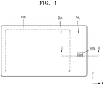
- FIG. 1 is a plan view of a display panel according to an embodiment
- FIG. 2 is a cross-sectional view taken along line II-II of FIG. 1
- FIG. 2 illustrates the display panel which is an organic light-emitting display panel including an organic light-emitting device 300.
- the display panel includes a substrate 100 including a display area DA and a peripheral area PA outside the display area DA, the peripheral area PA being a non-display area.
- a plurality of organic light-emitting devices 300 which are display elements, are arranged in the display area DA on the substrate 100.
- the substrate 100 may include at least one of various materials such as a glass material, a metal material and a plastic material, for example.
- a thin film transistor 210 is arranged in the display area DA of the substrate 100.
- the organic light-emitting device 300 electrically connected to the thin film transistor 210 may be arranged in the display area DA.
- the organic light-emitting device 300 may be electrically connected to the first thin film transistor 210 via a pixel electrode 310 which is electrically connected to the thin film transistor 210.
- a thin film transistor may be arranged in the peripheral area PA of the substrate 100.
- the thin film transistor arranged in the peripheral area PA may be, for example, a part of a circuit for controlling an electrical signal to be applied into the display area DA.
- the thin film transistor 210 includes a semiconductor layer 211, a gate electrode 213, a source electrode 215, and a drain electrode 217.
- the semiconductor layer 211 includes amorphous silicon, polycrystalline silicon, or an organic semiconductor material.
- a buffer layer 110 including a silicon oxide, a silicon nitride, or the like may be arranged on the substrate 100 to planarize a surface of the substrate 100 or to prevent impurities, etc. from penetrating into the semiconductor layer 211.
- the semiconductor layer 211 may be arranged on the buffer layer 110.
- the gate electrode 213 is disposed over the semiconductor layer 211 on the buffer layer 110.
- the source electrode 215 and the drain electrode 217 are electrically connected to each other in response to a signal applied to the gate electrode 213.
- the gate electrode 213 may have a single layer structure, or a multi-layer structure including, for example, at least one of aluminum (Al), platinum (Pt), palladium (Pd), silver (Ag), magnesium (Mg), gold (Au), nickel (Ni), neodymium (Nd), iridium (Ir), chromium (Cr), lithium (Li), calcium (Ca), molybdenum (Mo), titanium (Ti), tungsten (W), and copper (Cu), taking into account an adhesive property between the gate electrode 213 and a layer adjacent thereto, a surface smoothness of a surface of a layer to be stacked thereon, processability, etc.
- a gate insulating layer 120 including silicon oxide and/or a silicon nitride may be
- An interlayer insulating layer 130 may be disposed on the gate electrode 213.
- the interlayer insulating layer 130 may have a single layer structure, or a multi-layer structure including a silicon oxide, a silicon nitride, or the like.
- the source electrode 215 and the drain electrode 217 are disposed on the interlayer insulating layer 130.
- the source electrode 215 and the drain electrode 217 are electrically connected to the semiconductor layer 211 via respective contact holes defined in the interlayer insulating layer 130 and in the gate insulating layer 120.
- the source electrode 215 and the drain electrode 217 may have a single layer structure or a multi-layer structure including, for example, at least one of aluminum (Al), platinum (Pt), palladium (Pd), silver (Ag), magnesium (Mg), gold (Au), nickel (Ni), neodymium (Nd), iridium (Ir), chromium (Cr), lithium (Li), calcium (Ca), molybdenum (Mo), titanium (Ti), tungsten (W), and copper (Cu), taking into account a conductive property, etc.
- a protective film (not shown) may be disposed to cover the thin film transistor 210 to protect the thin film transistor 210 described above.
- the protective film may include, for example, an inorganic material such as a silicon oxide, a silicon nitride, a silicon oxynitride, etc.
- the protective film may have a single layer structure or a multi-layer structure.
- a planarization layer 140 may be disposed over the protective film.
- the planarization layer 140 may planarize an upper portion of the protective film covering the thin film transistor 210.
- the planarization layer 140 may include, for example, an organic material such as an acryl, benzocyclobutene ("BCB"), or hexamethyldisiloxane ("HMDSO").
- the planarization layer 140 may have a single layer, but embodiments are not limited thereto. Alternatively, the planarization layer 140 may have a multi-layer structure.
- the display device may include both the protective film and the planarization layer 140, or may include only one of the protective film and the planarization layer 140.
- the organic light-emitting device 300 is disposed on the planarization layer 140.
- the organic light-emitting device 300 includes the pixel electrode 310, an opposite electrode 330, and an intermediate layer 320 between the pixel electrode 310 and the opposite electrode 330 and including an emission layer.
- the pixel electrode 310 is provided on the planarization layer 140.
- the pixel electrode 310 is electrically connected to the thin film transistor 210 by contacting one of the source electrode 215 and the drain electrode 217 via the opening.
- the pixel electrode 310 may be a transparent (or semi-transparent) electrode, or may be a reflective electrode.
- the pixel electrode 310 may include, for example, indium tin oxide ("ITO"), indium zinc oxide ("IZO"), ZnO, In 2 O 3 , indium gallium oxide (“IGO”), and/or aluminum zinc oxide (“AZO").
- the pixel electrode 310 may include a reflective film including Ag, Mg, Al, Pt, Pd, Au, Ni, Nd, Ir, Cr, or a compound thereof, and a layer including ITO, IZO, ZnO, ln 2 O 3 , IGO, or AZO.
- the pixel electrode 310 may include various materials, and may have any of various structures, e.g., a single layer structure or a multi-layer structure.
- a pixel-defining film 150 may be disposed on the planarization layer 140.
- the pixel-defining film 150 defines a pixel with openings defined therein to correspond to respective sub-pixels, that is, openings exposing at least a central portion of the pixel electrode 310.
- the pixel-defining film 150 effectively prevents an arc, etc. from occurring at an edge of the pixel electrode 310 by increasing a distance between the edge of the pixel electrode 310 and the opposite electrode 330 over the pixel electrode 310.
- the pixel-defining film 150 may include, for example, an organic material such as polyimide ("PI”) or HMDSO.
- the intermediate layer 320 of the organic light-emitting device 300 may include a low molecular weight material, or a high molecular weight material.
- the intermediate layer 320 may have a stacked structure including at least one of a hole injection layer ("HIL"), a hole transport layer (“HTL”), an emission layer (“EML”), an electron transport layer (“ETL”), an electron injection layer (“EIL”), etc., and may include various organic materials, such as copper phthalocyanine (“CuPc”), N,N'-Di(naphthalene-1-yl)-N,N'-diphenyl-benzidine (“NPB”), tris-8-hydroxyquinoline aluminum (“Alq3”), etc.
- Such layers may be formed by vacuum deposition.
- the intermediate layer 320 may have a structure including an HTL and an EML.
- the HTL may include PEDOT
- the EML may include a polymeric material, such as poly-phenylenevinylene (“PPV”)-based polymeric material, a polyfluorene-based polymeric material, etc.
- the intermediate layer 320 may be formed by screen printing, inkjet printing, laser induced thermal imaging ("LITI”), etc.
- the intermediate layer 320 is not limited thereto, and may have any of various other structures.
- the opposite electrode 330 is disposed over the top of the display area DA, and may be arranged to cover the display area DA, as illustrated in FIG. 2 .
- the opposite electrode 330 may be integrally formed as a single unitary (and indivisible) body over the plurality of the organic light-emitting devices 300 and thus correspond to the plurality of organic light-emitting devices 300.
- the opposite electrode 330 may be a transparent (or semi-transparent) electrode, or may be a reflective electrode.
- the opposite electrode 330 may include a layer including a metal including a small work function (i.e., Li, Ca, LiF/Ca, LiF/AI, Al, Ag, Mg, or a compound thereof), and a transparent (semi-transparent) conductive layer including ITO, IZO, ZnO, In 2 O 3 , or the like.
- the opposite electrode 330 may include a layer of a sufficient thickness including Li, Ca, LiF/Ca, LiF/AI, Al, Ag, Mg, or a compound thereof.
- the opposite electrode 330 is not limited to the above structures and materials, and may be embodied in various different forms.
- the display panel includes the organic light-emitting device 300 as a display element, but embodiments are not limited thereto.
- the display element of the display panel includes a liquid crystal layer instead of the organic light-emitting device 300.
- the display panel may include a display element other than a display element including the organic light-emitting device 300 or the liquid crystal.
- a plurality of pads 700 are arranged in the peripheral area PA of the substrate 100 as illustrated in FIG. 1 .
- FIG. 1 illustrates only two pads 700, the embodiments are not limited thereto, and three or more pads 700 may be arranged adjacent to each other.
- each of the pads 700 may include a first conductive layer 710 and a second conductive layer 720.
- the first conductive layer 710 is disposed in a same layer as the source electrode 215 and the drain electrode 217, that is, on the interlayer insulating layer 130.
- the second conductive layer 720 is disposed in a same layer as the gate electrode 213, that is, on the gate insulating layer 120.
- the first conductive layer 710 may include a same material as the source electrode 215 and the drain electrode 217 and may be formed simultaneously with the source electrode 215 and the drain electrode 217 during a same manufacturing process.
- the second conductive layer 720 under the first conductive layer 710 may include a same material as the gate electrode 213 and may be formed simultaneously with the gate electrode 213 during a same manufacturing process.
- an opening corresponding to a central portion of the second conductive layer 720 may be defined through the interlayer insulating layer 130.
- the first conductive layer 710 may directly contact the second conductive layer 720 via the opening.
- Each of a plurality of first conductive layers 710 includes an upper surface 710a entirely exposed to an outside atmosphere.
- a pad division layer 140a between the first conductive layers 710 is disposed only between the first conductive layers 710 and may not cover the upper surface 710a of each of the first conductive layers 710 to expose the upper surface 710a of each first conductive layer 710 when the first conductive layers 710 is disposed on a corresponding second conductive layer 720.
- the pad division layer 140a has a thickness t2 different from a thickness t1 of the planarization layer 140
- the pad division layer 140a may include a same material as the planarization layer 140 and may be formed simultaneously with the planarization layer 140 during a same manufacturing process.
- first conductive layer 710 and/or the second conductive layer 720 may extend in a direction of the display area DA of the substrate 100 and may be electrically connected to the thin film transistor 210, etc. within the display area DA.
- FIG. 3 is a plan view of the first conductive layer 710 of FIGS. 1 and 2
- FIG. 4 is a cross-sectional view taken along line IV-IV of FIG. 3 .
- the first conductive layer 710 includes a main part 711 and a plurality of protrusions 712.
- the protrusions 712 are shaped to protrude from the main part 711 having an approximately rectangular shape in a direction approximately parallel to an upper surface of the substrate 100. Occurrence of a short circuit between adjacent first conductive layers 710 may be effectively prevented during a manufacturing process by allowing the first conductive layer 710 to be shaped in such a manner.
- the source electrode 215 and the drain electrode 217 of the thin film transistor 210, and the first conductive layer 710 may be formed by forming conductive layers having a multi-layer structure and patterning the formed conductive layers.
- conductive layers having a three-layered structure are formed and patterned to form the first conductive layer 710.
- Etching rates may be different in some of the conductive layers having the multi-layered structure.
- an etching rate of the aluminum layer is greater than an etching rate of the two titanium layers. Therefore, when the first conductive layer 710 is formed by forming a stacked structure of the titanium layer, the aluminum layer and the titanium layer, and etching the stacked structure, the aluminum layer is etched further than the titanium layer at the edge of the first conductive layer 710, and thus an edge of the aluminum layer becomes closer to a center of the first conductive layer 710 than an edge of the titanium layers.
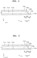
- the main part 711 of the first conductive layer 710 may include a lower main layer 711a, an intermediate main layer 711b on the lower main layer 711a, and an upper main layer 711c on the intermediate main layer 711b as illustrated in FIG. 4 .
- the lower main layer 711a and the upper main layer 711c may include titanium
- the intermediate main layer 711b may include aluminum.
- At least one of the protrusions 712 may have only a two-layered structure in at least a portion 712p thereof and may have a three-layered structure in a residual portion 712r, which is adjacent to the main part 711 as illustrated in FIG. 4 .
- the at least portion 712p may have a lower protrusion layer 712a and an intermediate protrusion layer 712b on the lower protrusion layer 712a
- the residual portion 712r may have the lower protrusion layer 712a, the intermediate protrusion layer 712b on the lower protrusion layer 712a, and an upper protrusion layer 712c on the intermediate protrusion layer 712b.
- the lower protrusion layer 712a and the upper protrusion layer 712c may include titanium
- the intermediate protrusion layer 712b may include aluminum.
- the protrusion 712 has the two-layered structure, not the three-layered structure in at least a portion thereof. This is because a portion of the upper protrusion layer 712c may be lost during a manufacturing process of the display panel.
- elements in the display area DA may be protected from external moisture or impurities, etc., by covering the elements in the display area DA with an encapsulation layer (not shown, refer to reference numeral 400 of FIG. 14 ).
- Elements in the peripheral area PA may be also protected from external moisture or impurities, etc., by covering the elements in the peripheral areas PA with the encapsulation layer (not shown).
- the pad 700 to which an electrical signal, etc., to be transferred to the display area DA to be applied, since an electronic device or a printed circuit board (“PCB”), etc. are electrically connected to the pad 700 afterwards, the pad 700 is not covered by the encapsulation layer, etc.
- a temporary protective film may be attached to the pad 700 to protect the pad 700 temporarily.
- the temporary protective film is detached afterwards when desired.
- the upper protrusion layer 712c may be lost in at least the portion 712p of the protrusion 712, and thus the protrusion 712 may have a two-layered structure, not a three-layered structure in at least the portion 712p.
- an etching rate of the intermediate protrusion layer 712b is higher than an etching rate of the upper protrusion layer 712c or the lower protrusion layer 712a and thus the intermediate protrusion layer 712b may not be left under the upper protrusion layer 712c at an edge of the protrusion 712, and in this case, the upper protrusion layer 712c corresponding to the relevant portion may be lost during an attachment/detachment process of the temporary protective film.
- the lost portion may be a conductive material having a long rod shape.
- the long rod-shaped conductive material may extend over adjacent first conductive layers 710 (in +y direction or -y direction) and thus cause a short circuit at the adjacent first conductive layers 710.
- the first conductive layer 710 includes the main part 711 and the plurality of protrusions 712.
- the first conductive layer 710 has an approximately zigzag shape at edges thereof.
- the lost portion is cut into a plurality of small conductive materials.
- a first side 712x and a second side 712y at an edge of the first conductive layer 710 may have a bent form, not a straight line form as illustrated in FIG.
- the first side 712x and the second side 712y are easily cut off from each other at the bent portion even when the uppermost layer is lost along the edge of the first conductive layer 710. Since the plurality of cut small conductive materials is small in size, such cut small conductive materials may not cause a short circuit at the adjacent first conductive layers 710. Therefore, in such an embodiment of the display panel, a defect rate may be substantially reduced during a manufacturing process.
- a width w of at least one of the protrusions 712 may be made smaller than a distance between the adjacent first conductive layers 710 to prevent a short circuit at the adjacent first conductive layers 710.
- each of the protrusions 712 may be made smaller than a distance between the adjacent first conductive layers 710.
- the distance between the adjacent first conductive layers 710 may be defined as a distance (a minimum distance) between edges of two adjacent first conductive layers 710 facing each other, not a distance between centers of the adjacent two first conductive layers 710. That is, the distance between the adjacent first conductive layers 710 may be defined as a width of a space between the two adjacent first conductive layers 710.
- a length of a small conductive material formed by cutting the protrusion 712 corresponds to the width w of the protrusion 712. Therefore, since a length of the small conductive material is smaller than the distance between the adjacent first conductive layers 710, occurrence of a short circuit between the adjacent first conductive layers 710 may be effectively prevented. In such an embodiment, the same or similar effect may be pursued by making a distance between the protrusions 712 smaller than the distance between the adjacent first conductive layers 710.
- a cross-sectional surface 712b' of the intermediate protrusion layer 712b may be relatively closer to a central portion (-x direction) of the first conductive layer 710 than a cross-sectional surface 712a' of the lower protrusion layer 712a in the protrusion 712.
- the lower main layer 711a and the lower protrusion layer 712a are integrally formed as a single unitary body, and the intermediate main layer 711b and the intermediate protrusion layer 712b are formed as single unitary body.
- At least one of the protrusions 712 may have a multi-layered structure that same as that of the main part 711. In one embodiment, for example, where the main part 711 has a three-layered structure, at least some of the protrusions 712 may have the same three-layered structure.
- conductive layers of a three-layered structure are formed and then patterned to form the first conductive layer 710.
- an etching rate of a layer arranged in the middle portion between the upper and lower portions is higher than an etching rate of layers arranged in the upper and lower portions, and thus a cross-sectional surface of the layer arranged in the middle may be relatively closer to a central portion of the first conductive layer 710 than a cross-sectional surface of the layers arranged in the upper and lower portions in an edge of the first conductive layer 710. Accordingly, FIG.
- FIG. 5 illustrates that a cross-sectional surface 712b' of the intermediate protrusion layer 712b is relatively closer to a central portion (-x direction) of the first conductive layer 710 than a cross-sectional surface 712a' of the lower protrusion layer 712a of the protrusion 712. Therefore, an empty space may be formed under the upper protrusion layer 712c at the portion 712p of the protrusion 712.
- the upper protrusion layer 712c may not be lost in some of the protrusions 712 because the first side 712x and the second side 712y have a bent form, not a straight line form, at the edge of the first conductive layer 710, as described above with reference to FIG. 3 , and thus uppermost layers may be easily cut off from each other at the bent portion even when the uppermost layers are lost along the edge of the first conductive layer 710.
- an uppermost layer may remain along an edge of the first conductive layer 710 in some of the protrusions 712.
- a third side 710z (see FIG. 3 ) of the first conductive layer 710 which may be an edge of the main part 711 between the protrusions 712, may have the same layered structure as that of the portion 712p having only the two-layered structure among the portions of the protrusion 712 of FIG. 4 .
- the first side 712x, the second side 712y and the third side 710z have bent form, not straight line forms at the edges of the first conductive layer 710, even when uppermost layers are lost along the edges of the first conductive layer 710, the uppermost layers may be easily cut off from each other at the portions defined by the bent side lines. Therefore, occurrence of a short circuit at adjacent pads 700 may be effectively prevented.
- the main part 711 may have a two-layered structure including the lower main layer 711a and the upper main layer 711c, and at least one of the protrusions 712 may have only the lower protrusion layer 712a in at least the portion 712p to have only a one-layered structure.
- the protrusion 712 may have the lower protrusion layer 712a and the upper protrusion layer 712c in the residual portion 712r thereof in a direction of the main part 711.
- the lower main layer 711a and the lower protrusion 712a may integrally be formed as a single unitary body.
- FIG. 7 which is a cross-sectional view of a first conductive layer of a display panel at least one protrusion 712 may have the same two-layered structure as that of the main part 711, as in the embodiments described above with reference to FIG. 5 .
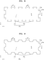
- FIG. 8 is a plan view of a first conductive layer of a display panel according to an alternative embodiment.
- a width w1 of a distal portion of the plurality of protrusions 712 in a direction away from the main part 711 is greater than a width w2 of a proximal portion of the plurality of protrusions 712 in a direction toward the main part 711.
- the first side 712x and the second side 712y in an edge of the first conductive layer 710 have a bent form or collectively define a bent side line, not a straight line form (i.e., not linearly aligned), and further, an angle formed by the first side 712x and the second side 712y may be an acute angle. Consequently, even when an uppermost layer is lost along the edge of the first conductive layer 710, since an angle of the portion defined by bent side lines is a pointed acute angle, the uppermost layer at that portion may be more easily cut off.
- a cross-section taken along line IV-IV of the first conductive layer 710 of FIG. 8 may be substantially the same as that described above with reference to FIG. 4 , and that described above with reference to FIGS. 5 to 7 , and any repetitive detailed description thereof will be omitted.
- FIG. 9 is a plan view of a first conductive layer of a display panel according to another alternative embodiment.
- a width w1 of a distal portion of the plurality of protrusions 712 in a direction away from the main part 711 is less than a width w2 of a proximal portion of the plurality of protrusions 712 in a direction toward the main part 711.
- a portion of the protrusions 712 in which a probability that an uppermost layer thereof will be lost is high is an uppermost layer arranged in a distal portion in a direction away from the main part 711, that is, an uppermost layer of the first side 712x. Since an uppermost layer of the second side 712y is adjacent to an uppermost layer of the main part 711, the uppermost layer of the second side 712y is connected to the uppermost layer of the main part 711 and thus a probability that the uppermost layer of the second side 712y is not lost is high.
- occurrence of a short circuit between adjacent first conductive layers 710 may be effectively prevented by reducing a size of an uppermost layer arranged at the distal portion, and having a high probability that the uppermost layer will be lost even when the portion of the uppermost layer is lost.
- a cross-section taken along line IV-IV of the first conductive layer 710 of FIG. 9 may be substantially the same as that described above with reference to FIG. 4 and that described above with reference to FIGS. 5 to 7 , and any repetitive detailed description thereof will be omitted.
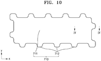
- the protrusions 712 of the first conductive layer 710 may not have a pointed form when viewed from a plan view in a direction approximately perpendicular to the substrate 100.
- the protrusions 712 may have a smooth curve-shaped edge without being pointed, when viewed from a plan view.
- an edge of a portion at which the main part 711 is connected to the protrusion 712 may have a smooth-curved shape, as shown in FIG. 10 .
- an edge of the first conductive layer 710 may have a smooth form without a pointed portion, when viewed a plan view viewed in a direction approximately perpendicular to the substrate 100.
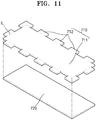
- FIG. 11 is an exploded perspective view of the first conductive layer 710 and the second conductive layer 720 of a display panel according to an embodiment. For convenience of illustration, FIG. 11 illustrates that the first conductive layer 710 has a flat form, rather than having curved portions.
- an edge of the main part 711 of the first conductive layer 710 may be represented by an imaginary line IL.
- an orthogonal projection of an edge of the main part 711 of the first conductive layer 710 onto a substrate (not shown) (arranged in -z direction) may overlap an orthogonal projection of an edge of the second conductive layer 720 onto the substrate, arranged (-z direction) under the first conductive layer 710 and having a shape corresponding to the main part 711.
- an orthogonal projection of the protrusions 712 of the first conductive layer 710 onto the substrate may be arranged outside an orthogonal projection of an edge of the second conductive layer 720 onto the substrate. In such an embodiment, an area of contact between the first conductive layer 710 and the second conductive layer 720 may be sufficient.
- an edge of the second conductive layer 720 may be arranged outside the main part 711 of the first conductive layer 710 and may be arranged in the vicinity of a center of each of the protrusions 712.
- the second conductive layer 720 may have an area greater than that of the main part 711 of the first conductive layer 710, and an orthogonal projection of an edge of the protrusions 712 of the first conductive layer 710 in a direction farthest away from the main part 711 onto the substrate may be arranged outside an orthogonal projection of an edge of the second conductive layer 720 onto the substrate.
- FIG. 12 illustrates that the first conductive layer 710 has a flat form, rather than having curved portions.
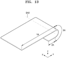
- the display panel may be bent.
- the substrate 100 of the display panel includes a bending area BA extending in a first direction (+y direction).
- the bending area BA is arranged between a first area 1A and a second area 2A in a second direction (+x direction) crossing the first direction.
- the substrate 100 is bent around a bending axis BAX extending in the first direction (+y direction) as illustrated in FIG. 13 .
- the substrate 100 may include at least one of various materials having flexible or bendable characteristics, e.g., polymer resins such as polyethersulphone (“PES”), polyacrylate (“PAR”), polyetherimide (“PEI”), polyethylene napthalate (“PEN”), polyethyleneterephthalate (“PET”), polyphenylene sulfide (“PPS”), polyarylate (“PAR”), PI, polycarbonate (“PC”), or cellulose acetate propionate (“CAP”).
- polymer resins such as polyethersulphone (“PES”), polyacrylate (“PAR”), polyetherimide (“PEI”), polyethylene napthalate (“PEN”), polyethyleneterephthalate (“PET”), polyphenylene sulfide (“PPS”), polyarylate (“PAR”), PI, polycarbonate (“PC”), or cellulose acetate propionate (“CAP”).
- PES polyethersulphone
- PAR polyacrylate
- PEI polyetherimide
- PEN polyethylene napthalate
- the substrate 100 may have a multi-layered structure including two layers, each including a polymer resin, and a barrier layer including an inorganic material (such as a silicon oxide, a silicon nitride, a silicon oxynitride, etc.) between the two layers, but not being limited thereto.
- the substrate 100 may be modified variously.
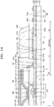
- FIG. 14 is a cross-sectional view of the portion of the display panel of FIG. 13 .
- the first area 1A includes a display area DA.
- the first area 1A may include, in addition to the display area DA, a portion of the non-display area outside the display area DA.
- the second area 2A also includes the non-display area. Configurations of the display area DA, the first conductive layer 710 and/or the second conductive layer 720, etc. are the same as those described above with reference to FIG. 2 , and modifications described above with reference to FIGS. 3 to 12 are applicable to such an embodiment of the display panel.
- the encapsulation layer 400 may cover display elements to protect the display elements such as the organic light-emitting device 300 in the display area DA.
- the pad 700 in the case of the pad 700 to which an electrical signal, etc. to be transferred to the display area DA will be applied, the pad 700 is desired not to be covered by the encapsulation layer 400, etc., to allow an electronic device or a PCB, etc. to be electrically connected to the pad 700 afterwards. Therefore, the upper surface 710a of the first conductive layer 710 is entirely exposed to the outside.
- the encapsulation layer 400 may include a first inorganic encapsulation layer 410, an organic encapsulation layer 420, and a second inorganic encapsulation layer 430 as illustrated in FIG. 14 .
- the first inorganic encapsulation layer 410 may cover the opposite electrode 330 and include a silicon oxide, a silicon nitride, and/or a silicon oxynitride. Alternatively, other layers such as a capping layer may be selectively provided between the first inorganic encapsulation layer 410 and the opposite electrode 330. Since the first inorganic encapsulation layer 410 is provided along a structure thereunder, an upper surface of the first inorganic encapsulation layer 410 is not flat as illustrated in FIG. 14 .
- the organic encapsulation layer 420 covers the first inorganic encapsulation layer 410. In such an embodiment, the organic encapsulation layer 420 may have an approximately even upper surface.
- the organic encapsulation layer 420 may have an approximately even upper surface at a portion corresponding to the display area DA.
- the organic encapsulation layer 420 may include at least one of PET, PEN, PC, PI, polyethylene sulfonate, polyoxymethylene, PAR, and HMDSO.
- the second inorganic encapsulation layer 430 may cover the organic encapsulation layer 420 and include a silicon oxide, a silicon nitride, and/or a silicon oxynitride.
- the second inorganic encapsulation layer 430 may cover the organic encapsulation layer 420 to ensure that the organic encapsulation layer 420 is not exposed to the outside by contacting the first inorganic encapsulation layer 410 at an edge thereof arranged outside the display area DA.
- the encapsulation layer 400 may include the first inorganic encapsulation layer 410, the organic encapsulation layer 420 and the second inorganic encapsulation layer 430.
- the crack may be disconnected between the first inorganic encapsulation layer 410 and the organic encapsulation layer 420 or between the organic encapsulation layer 420 and the second inorganic encapsulation layer 430 through the above multi-layered structure.
- forming of a path through which external moisture or oxygen may infiltrate into the display area DA may be effectively prevented or substantially reduced.
- a polarization plate 520 may be arranged on the encapsulation layer 400 by using an optically clear adhesive ("OCA") 510.
- OCA optically clear adhesive
- the polarization plate 520 may reduce reflection of external light.
- the external light that has passed through the polarization plate 520 is reflected by an upper surface of the opposite electrode 330 and then passes through the polarization plate 520 again, the external light passes through the polarization plate 520 twice and the phase of the external light may be changed. Therefore, the phase of reflected light may be different from the phase of the external light entering the polarization plate 520 and thus destructive interference occurs. Accordingly, the reflection of the external light may be reduced and visibility may be improved due to the destructive interference.
- the OCA 510 and the polarization plate 520 may cover an opening (a discontinuous region) in the planarization layer 140 outside the display area DA as shown in FIG. 14 .
- the polarization plate 520 may be omitted.
- the polarization plate 520 may be omitted and selectively replaced with another element.
- the polarization plate 520 may be omitted, and instead, a black matrix and a color filter may be provided to reduce the reflection of external light.
- the buffer layer 110, the gate insulating layer 120 and the interlayer insulating layer 130, each of which includes an inorganic material, will be collectively referred as inorganic insulating layers.
- an opening corresponding to the bending area BA is defined through the inorganic insulating layers, as illustrated in FIG. 14 .
- openings 110a, 120a and 130a are defined through the buffer layer 110, the gate insulating layer 120 and the interlayer insulating layer 130, respectively, to correspond to the bending area BA, e.g., to overlap the bending area BA when viewed from a plan view.
- an area of each opening may be wider than that of the bending area BA.
- a width OW of an opening is wider than a width BAw of the bending area BA.
- the area of the opening may be defined as an area of an opening having a smallest area among the openings 110a, 120a and 130a of the buffer layer 110, the gate insulating layer 120 and the interlayer insulating layer 130.
- the area of the opening is defined by the area of the opening 110a of the buffer layer 110.
- the opening 120a of the gate insulating layer 120 and the opening 130a of the interlayer insulating layer 130 may be simultaneously formed.
- contact holes is desired to be formed through the gate insulating layer 120 and the interlayer insulating layer 130.
- the opening 120a of the gate insulating layer 120 and the opening 130a of the interlayer insulating layer 130 may be simultaneously formed. Accordingly, an inner surface of the opening 120a of the gate insulating layer 120 and an inner surface of the opening 130a of the interlayer insulating layer 130 may form a continuous plane as illustrated in FIG. 14 .
- the display panel includes an organic material layer 160 filling at least a portion of the inorganic insulating layers. In an embodiment, as shown in FIG. 14 , the organic material layer 160 may completely fill the opening.
- the display panel includes a connection wire layer 215c.
- the connection wire layer 215c may extend from the first area 1A to the second area 2A via the bending area BA and is arranged on the organic material layer 160. In an embodiment, where the organic material layer 160 is absent, the connection wire layer 215c may be arranged on the inorganic insulating layer such as the interlayer insulating layer 130.
- connection wire layer 215c may include a same material as that of the source electrode 215 or the drain electrode 217, and may be formed simultaneously with the source electrode 215 or the drain electrode 217.
- the first conductive layer 710 may include a same material as that of the connection wire layer 215c, and may be formed simultaneously with the connection wire layer 215c.
- the display panel is not bent, but not being limited thereto.
- the substrate 100, etc. are bent in the bending area BA as illustrated in FIG. 13 .
- the display panel is manufactured such that the substrate 100 is approximately flat as illustrated in FIG. 14 during the manufacturing process, and thereafter, the display panel may be shaped as illustrated in FIG. 13 through bending of the substrate 100, etc. in the bending area BA.
- tensile stress may be applied to the connection wire layer 215c while the substrate 100, etc. are bent in the bending area BA, occurrence of a defect in the connection wire layer 215c during the bending process may be effectively prevented or substantially reduced.
- the inorganic insulating layers such as the buffer layer 110, the gate insulating layer 120 and/or the interlayer insulating layer 130 do not have openings and thus have continuous shapes over the first area 1A to the second area 2A, and the connection wire layer 215c is arranged on the inorganic insulating layers, a large amount of tensile stress may be applied to the connection wire layer 215c while the substrate 100, etc. are bent during a manufacturing process.
- a crack, etc. is likely to occur in the inorganic insulating layers in the bending area BA.
- a crack occurs in the inorganic insulating layers, a crack, etc. occur in the connection wire layer 215c on the inorganic insulating layers and thus a probability of occurrence of a defect such as disconnection, etc. of the connection wire layer 215c is very high.
- an opening is defined through the inorganic insulating layer in the bending area BA, and a portion of the connection wire layer 215c corresponding to the bending area BA is arranged on the organic material layer 160 filling at least a portion of the opening of the inorganic insulating layer as described above. Since an opening is defined through the inorganic insulating layer in the bending area BA, a probability of occurrence of a crack, etc. in the inorganic insulating layer is substantially low, and the organic material layer 160 has a characteristic of including an organic material and thus a probability of occurrence of a crack is low. Therefore, occurrence of a crack, etc.
- the organic material layer 160 has a hardness less than that of an inorganic material layer and thus may absorb tensile stress generated due to bending of the substrate 100, etc. and effectively reduce concentration of tensile stress on the connection wire layer 215c.
- FIG. 14 illustrates an embodiment, where an opening is defined through the inorganic insulating layers
- the embodiment is not limited thereto.
- the inorganic insulating layers may have a groove instead of an opening.
- no opening is defined through the buffer layer 110
- the buffer layer 110 extends from the first area 1A to the second area 2A via the bending area BA
- the openings 120a and 130a are defined only through the gate insulating layer 120 and the interlayer insulating layer 130, respectively.
- the buffer layer 110, the gate insulating layer 120 and the interlayer insulating layer 130, each including an inorganic material may be collectively referred to as inorganic insulating layers.
- the inorganic insulating layers may be understood as having a groove corresponding to the bending area BA.
- the organic material layer 160 may fill a portion of the groove.
- the display panel may include additional connection wire layers 213a and 213b in addition to the connection wire layer 215c.
- the additional connection wire layers 213a and 213b may be arranged in the first area 1A or the second area 2A such that the additional connection wire layers 213a and 213b are arranged in a layer different from the layer in which the connection wire layer 215c is arranged, and may be electrically connected to the connection wire layer 215c.
- FIG. 14 illustrates that the additional connection wire layers 213a and 213b include a same material as that of the gate electrode 213 of the thin film transistor 210 and are arranged in the layer in which the gate electrode 213 is arranged.
- the additional connection wire layers 213a and 213b are arranged on the gate insulating layer 120.
- the connection wire layer 215c may contact the additional connection wire layers 213a and 213b via contact holes of the interlayer insulating layer 130.
- the additional connection wire layer 213a and the additional connection wire layer 213b may be arranged in the first area 1A and the second area 2A, respectively.
- the second conductive layer 720 may include a same material as that of the additional connection wire layers 213a and 213b, and may be formed simultaneously with the additional connection wire layers 213a and 213b.
- the second conductive layer 720 and the additional connection wire layers 213a and 213b may be integrally formed as a single unitary body.
- the additional connection wire layer 213a arranged in the first area 1A may be electrically connected to the thin film transistor, etc. within the display area DA, and thus, the connection wire layer 215c may be electrically connected to the thin film transistor, etc., within the display area DA via the additional connection wire layer 213a.
- the additional connection wire layer 213b may be electrically connected to the thin film transistor, etc., within the display area DA via the connection wire layer 215c.
- the additional connection wire layers 213a and 213b may be electrically connected to elements arranged inside the display area DA while the additional connection wire layers 213a and 213b are arranged outside the display area DA.
- the additional connection wire layers 213a and 213b may extend in a direction of the display area DA and at least a portion of the additional connection wire layers 213a and 213b may be arranged inside the display area DA.
- a bending protection layer (“BPL") 600 may be arranged outside the display area DA.
- the BPL 600 may be arranged over the connection wire layer 215c in a region corresponding to at least the bending area BA.
- a stress-neutral plane exists within the stacked body. If the BPL 600 is absent, excessive tensile stress, etc., may be applied to the connection wire layer 215c within the bending area BA while the substrate 100, etc. are bent. This is because a location of the connection wire layer 215c may not correspond to a stress-neutral plane. However, a location of a stress-neutral plane may be adjusted in a stacked body including all of the substrate 100, the connection wire layer 215c, the BPL 600, etc., by providing the BPL 600 and by adjusting a thickness and a modulus of the BPL 600.
- connection wire layer 215c may be minimized or compression stress may be applied to the connection wire layer 215c by allowing a stress-neutral plane to be arranged in the vicinity of or over the connection wire layer 215c via the BPL 600.
- the BPL 600 may include an acryl.
- a probability that the connection wire layer 215c is damaged by the compression stress is extremely low compared to a case where tensile stress is applied to the connection wire layer 215c.
- the BPL 600 since an electronic device or a PCB, etc. is desired to be electrically connected to the pad 700 to transfer an electrical signal, etc. to the display area DA afterwards, the BPL 600 does not cover the first conductive layer 710. Therefore, an upper surface 710a of the first conductive layer 710 is entirely exposed to the outside.
- the embodiments of the invention are not limited thereto. That is, a display device including the display panel as an element thereof is included in the scope of the disclosure.
- FIG. 15 is a cross-sectional view of a display device according to another alternative embodiment.
- the display device includes the display panel corresponding to one of the above-described embodiments or modifications, and a conductive material layer directly contacting an upper surface (+z direction) of the first conductive layer 710 of the display panel.
- the display device includes the substrate 100 including the display area DA and the peripheral area PA outside the display area DA, the first conductive layer 710, and a conductive material layer.
- the first conductive layer 710 is arranged in the peripheral area PA and an edge of an upper surface of the first conductive layer 710 is not covered by an insulating layer such as the pad division layer 140a.
- the first conductive layer 710 includes the main part 711 (see FIGS.
- the conductive material layer directly contacts an upper surface of the first conductive layer 710.
- FIG. 15 illustrates a bump 910 under a body 920 of an electronic device 900 such as an integrated circuit device as a conductive material layer directly contacting an upper surface of the first conductive layer 710.
- the conductive material layer may be a conductive adhesive layer.
- the conductive material layer may be an anisotropic conductive film (“ACF") 800 including a conductive ball 810.
- ACF anisotropic conductive film
- the bump 910 under the body 920 of the electronic device 900 contacts the conductive ball 810 of the ACF 800, and the conductive ball 810 contacts an upper surface of the first conductive layer 710. Therefore, the bump 910 of the electronic device 900 is electrically connected to the first conductive layer 710.
- the conductive material layer may be a conductive adhesive layer as well as the ACF 800.
- the first conductive layer 710 may have a shape extending in a predetermined direction (e.g., a direction parallel to x-axis).
- a central axis CL of the first conductive layer 710 may be parallel to the predetermined direction (x-axis direction) in which the first conductive layer 710 extends.
- a conductive adhesive layer such as the ACF 800 may cover an entire upper surface of the first conductive layer 710 in a direction (y-axis direction) crossing the central axis CL of the first conductive layer 710.
- the conductive adhesive layer or the ACF 800 may completely cover an upper surface of some of the protrusions 712 of the first conductive layer 710.
- a portion of an upper surface of the first conductive layer 710 may not be covered by the conductive adhesive layer. That is, it may be understood that an entire upper surface of at least one of the protrusions 712 of the first conductive layer 710 is covered by the conductive adhesive layer.
- the display device may prevent occurrence of a short circuit between the adjacent first conductive layers 710 during a manufacturing process.
- FIGS. 15 and 16 show embodiments where the display device includes the electronic device 900, embodiments are not limited thereto.
- the display device may include a PCB including pads electrically connected to the first conductive layer 710 and may be modified variously.
- an edge of an upper surface of the first conductive layer 710 of the pad 700 is not covered by the pad division layer 140a, etc. as described above, and the upper surface of the first conductive layer 710 is exposed.
- This is for the purpose of securing a minimum area via which the pad 700 is exposed under conditions in which an area of the peripheral area PA is reduce, and not the display area DA in the display panel. If an area exposing the pad 700 of the display panel is reduced, an area in which the bump, etc. of the electronic device 900 contact the pad 700 of the display panel is reduced, and thus alignment of the bump, etc. of the electronic device 900 and the pad 700 of the display panel may not be effectively performed.
- the number of the pads 700 of the display panel may increase. Therefore, to sufficiently secure an area via which each of the pads 700 is exposed while arranging a greater number of pads 700 in a limited area of the peripheral area PA, an entire upper surface of the first conductive layer 710 of the pad 700 is desired to be exposed as described above.
- an edge of an upper surface of the first conductive layer 710 of the pad 700 may not be covered by the pad division layer 140a by making a thickness t2 of the pad division layer 140a including a same material as that of the planarization layer 140 less than a thickness t1 of the planarization layer 140.
- the pad division layer 140a may not be provided at a portion where the pad 700 is arranged, and in the vicinity of the pad 700, a layer, for example, the interlayer insulating layer 130 arranged under the first conductive layer 710 of the pad 700 may be exposed as an uppermost layer to the outside when needed.
- Embodiment of the display device shown in FIGS. 15 to 17 may include an embodiment of a display panel described above with reference to FIGS. 1 to 14 . That is, as far as the display device includes one of the display panels described with reference to FIGS. 1 to 14 , an embodiment of a display panel and modifications thereof, and the conductive material layer directly contacting an upper surface of the first conductive layer 710, the display device belongs to the display device according to the embodiments.
Landscapes
- Physics & Mathematics (AREA)
- Nonlinear Science (AREA)
- Engineering & Computer Science (AREA)
- Microelectronics & Electronic Packaging (AREA)
- Chemical & Material Sciences (AREA)
- Optics & Photonics (AREA)
- Mathematical Physics (AREA)
- Crystallography & Structural Chemistry (AREA)
- General Physics & Mathematics (AREA)
- Inorganic Chemistry (AREA)
- Devices For Indicating Variable Information By Combining Individual Elements (AREA)
- Electroluminescent Light Sources (AREA)
Abstract
Description
- One or more embodiments relate to a display panel and a display device including the display panel, and more particularly, to a display panel in which a short circuit occurrence rate is reduced in a pad unit thereof, and a display device including the display panel.
- A display panel is a display unit which displays an image by receiving information about the image. Such a display panel typically includes, at an edge thereof, pads electrically connected to display elements to receive information about an image, etc., and such pads are electrically connected to pads of a printed circuit board, or bumps of electronic elements, etc. The pads of the display panel may be desired to be electrically connected to predetermined pads of the printed circuit board or the bumps of the electronic elements without short circuit between the pads of the display panel.
- In a conventional display panel, adjacent pads therein may be electrically connected to each other and a short circuit may occur.
- One or more embodiments include a display panel in which a short circuit occurrence rate is reduced in a pad unit thereof, and a display device including the display panel.
- According to one or more embodiments, a display panel includes: a substrate including a display area and a peripheral area outside; and a first conductive layer in the peripheral area, where an entire upper surface of the first conductive layer is exposed to an outside of the display panel, and the first conductive layer includes a main part and a plurality of protrusions protruding from the main part in a direction parallel to an upper surface of the substrate.
- In an embodiment, at least a portion of the main part may have a three-layered structure, and at least a portion of a protrusion of the plurality of protrusions may have a two-layered structure.
- In an embodiment, the three-layered structure of the at least a portion of the main part may be defined by a lower main layer, an intermediate main layer on the lower main layer, and an upper main layer on the intermediate main layer, and the two-layered structure of the at least a portion of the protrusion may be defined by a lower protrusion layer and an intermediate protrusion layer on the lower protrusion layer.
- In an embodiment, the lower main layer and the lower protrusion layer may be integrally formed as a single unitary body, and the intermediate main layer and the intermediate protrusion layer may be integrally formed as a single unitary body.
- In an embodiment, an outer side of the intermediate protrusion layer may be closer to a center of the main part than an outer side of the lower protrusion layer is.
- In an embodiment, at least a portion of the main part may have a two-layered structure, and at least a portion of a protrusion of the plurality of protrusions may have a single-layered structure.
- In an embodiment, the two-layered structure of the at least a portion of the main part may be defined by a lower main layer and an upper main layer on the lower main layer, and the single-layered structure of the at least a portion of the protrusion may be defined by a lower protrusion layer.
- In an embodiment, the lower main layer and the lower protrusion layer may be integrally formed as a single unitary body.
- In an embodiment, a width of a distal portion of the plurality of protrusions in a direction away from the main part may be greater than a width of a proximal portion of the plurality of protrusions in a direction toward the main part.
- In an embodiment, a width of a distal portion of the plurality of protrusions in a direction away from the main part may be less than a width of a proximal portion of the plurality of protrusions in a direction toward the main part.
- In an embodiment, at least a portion of the main part may have a multi-layered structure, and at least a portion of a protrusion of the plurality of protrusions may have a multi-layered structure the same as the multi-layered structure of the at least a portion of the main part.
- In an embodiment, the display panel may further include a second conductive layer under the first conductive layer and having a shape corresponding to a shape of the main part.
- In an embodiment, an orthogonal projection of an edge of the main part onto the substrate may overlap an orthogonal projection of an edge of the second conductive layer in the direction toward the substrate.
- In an embodiment, the display panel may further include an insulating layer between the first conductive layer and the second conductive layer, an opening may be defined through the insulating layer, and a central portion of the second conductive layer may directly contact a central portion of the main part via the opening.
- In an embodiment, an orthogonal projection of the plurality of protrusions onto the substrate may be located outside an orthogonal projection of an edge of the second conductive layer onto the substrate.
- In an embodiment, a width of at least one of the plurality of protrusions may be less than a distance between the first conductive layer and a conductive layer adjacent to the first conductive layer.
- According to one or more embodiments, a display device includes: a substrate including a display area and a peripheral area outside the display area; a first conductive layer in the peripheral area, where the first conductive layer includes a main part and a plurality of protrusions protruding from the main part in a direction parallel to an upper surface of the substrate, where an edge of an upper surface of the first conductive layer is not covered by an insulating layer; and a conductive material layer directly contacting the upper surface of the first conductive layer.
- In an embodiment, at least a portion of the main part may have a three-layered structure, and at least a portion of a protrusion of the plurality of protrusions may have a two-layered structure.
- In an embodiment, the three-layered structure of the at least a portion of the main part may be defined by a lower main layer, an intermediate main layer on the lower main layer, and an upper main layer on the intermediate main layer, and the two-layered structure of the at least a portion of the protrusion may be defined by a lower protrusion layer and an intermediate protrusion layer on the lower protrusion layer.
- In an embodiment, the lower main layer and the lower protrusion layer may be integrally formed as a single unitary body, and the intermediate main layer and the intermediate protrusion layer may be integrally formed as a single unitary body.
- In an embodiment, an outer side of the intermediate protrusion layer may be closer to a center of the main layer than an outer side of the lower protrusion layer is.
- In an embodiment, at least a portion of the main part may have a two-layered structure, and at least a portion of a protrusion of the plurality of protrusions may have a single-layered structure.
- In an embodiment, the two-layered structure of the at least a portion of the main part may be defined by a lower main layer and an upper main layer on the lower main layer, and the single-layered structure of at a portion of the protrusion may be defined by a lower protrusion layer.
- In an embodiment, the lower main layer and the lower protrusion layer may be integrally formed as a single unitary body.
- In an embodiment, a width of a distal portion of the plurality of protrusions in a direction away from the main part may be greater than a width of a proximal portion of the plurality of protrusions in a direction toward the main part.
- In an embodiment, a width of a distal portion of the plurality of protrusions in a direction away from the main part may be less than a width of a proximal portion of the plurality of protrusions in a direction toward the main part.
- In an embodiment, at least a portion of the main part may have a multi-layered structure, and at least a portion of a protrusion of the plurality of protrusions may have a multi-layered structure the same as the multi-layered structure of the main part.
- In an embodiment, the display panel may further include a second conductive layer under the first conductive layer and having a shape corresponding to a shape of the main part.
- In an embodiment, an orthogonal projection of an edge of the main part onto the substrate may overlap an orthogonal projection of an edge of the second conductive layer onto the substrate.
- In an embodiment, the display panel may further include an insulating layer between the first conductive layer and the second conductive layer, an opening may be defined through the insulating layer, and a central portion of the second conductive layer may directly contact a central portion of the main part via the opening.
- In an embodiment, an orthogonal projection of the plurality of protrusions onto the substrate may be located outside an orthogonal projection of an edge of the second conductive layer onto the substrate.
- In an embodiment, a width of at least one of the plurality of protrusions may be less than a distance between the first conductive layer and a conductive layer adjacent to the first conductive layer.
- In an embodiment, the conductive material layer may be a conductive adhesive layer.
- In an embodiment, the conductive adhesive layer may cover an entire upper surface of at least one of the plurality of protrusions.
- In an embodiment, the conductive material layer may be a bump of an electronic element or a pad of a printed circuit board.
- In an embodiment, the conductive material layer may be a portion of an integrated circuit element.
- According to embodiments of the invention, a display panel in which a short circuit occurrence rate is reduced in a pad unit thereof, and a display device including the display panel may be implemented.
- These and/or other features will become apparent and more readily appreciated from the following description of the embodiments, taken in conjunction with the accompanying drawings, in which:
-
FIG. 1 is a plan view of a display panel according to an embodiment; -
FIG. 2 is a cross-sectional view taken along line II-II ofFIG. 1 ; -
FIG. 3 is a plan view of a first conductive layer ofFIGS. 1 and2 ; -
FIG. 4 is a cross-sectional view taken along line IV-IV ofFIG. 3 ; -
FIG. 5 is a cross-sectional view of a first conductive layer of a display panel according to an alternative embodiment; -
FIG. 6 is a cross-sectional view of a first conductive layer of a display panel according to another alternative embodiment; -
FIG. 7 is a cross-sectional view of a first conductive layer of a display panel according to still another alternative embodiment; -
FIG. 8 is a plan view of a first conductive layer of a display panel according to another alternative embodiment; -
FIG. 9 is a plan view of a first conductive layer of a display panel according to yet another alternative embodiment; -
FIG. 10 is a plan view of a first conductive layer of a display panel according to yet another alternative embodiment; -
FIG. 11 is an exploded perspective view of a first conductive layer and a second conductive layer of a display panel according to an embodiment; -
FIG. 12 is an exploded perspective view of a first conductive layer and a second conductive layer of a display panel according to an alternative embodiment; -
FIG. 13 is a perspective view of a portion of a display panel according to an alternative embodiment; -
FIG. 14 is a cross-sectional view of the portion of the display panel ofFIG. 13 ; -
FIG. 15 is a cross-sectional view of a display device according to another alternative embodiment; -
FIG. 16 is a cross-sectional view of a display device according to another alternative embodiment; and -
FIG. 17 is a plan view of a first conductive layer of a display device according to another alternative embodiment. - The invention now will be described more fully hereinafter with reference to the accompanying drawings, in which various embodiments are shown. This invention may, however, be embodied in many different forms, and should not be construed as limited to the embodiments set forth herein. Rather, these embodiments are provided so that this disclosure will be thorough and complete, and will fully convey the scope of the invention to those skilled in the art. Like reference numerals refer to like elements throughout.
- It will be understood that when an element is referred to as being "on" another element, it can be directly on the other element or intervening elements may be present therebetween. In contrast, when an element is referred to as being "directly on" another element, there are no intervening elements present.
- It will be understood that, although the terms "first," "second," "third" etc. may be used herein to describe various elements, components, regions, layers and/or sections, these elements, components, regions, layers and/or sections should not be limited by these terms. These terms are only used to distinguish one element, component, region, layer or section from another element, component, region, layer or section. Thus, "a first element," "component," "region," "layer" or "section" discussed below could be termed a second element, component, region, layer or section without departing from the teachings herein.
- The terminology used herein is for the purpose of describing particular embodiments only and is not intended to be limiting. As used herein, the singular forms "a," "an," and "the" are intended to include the plural forms, including "at least one," unless the content clearly indicates otherwise. "Or" means "and/or." As used herein, the term "and/or" includes any and all combinations of one or more of the associated listed items. It will be further understood that the terms "comprises" and/or "comprising," or "includes" and/or "including" when used in this specification, specify the presence of stated features, regions, integers, steps, operations, elements, and/or components, but do not preclude the presence or addition of one or more other features, regions, integers, steps, operations, elements, components, and/or groups thereof.
- Furthermore, relative terms, such as "lower" or "bottom" and "upper" or "top," may be used herein to describe one element's relationship to another elements as illustrated in the Figures. It will be understood that relative terms are intended to encompass different orientations of the device in addition to the orientation depicted in the Figures. For example, if the device in one of the figures is turned over, elements described as being on the "lower" side of other elements would then be oriented on "upper" sides of the other elements. The exemplary term "lower," can therefore, encompasses both an orientation of "lower" and "upper," depending on the particular orientation of the figure. Similarly, if the device in one of the figures is turned over, elements described as "below" or "beneath" other elements would then be oriented "above" the other elements. The exemplary terms "below" or "beneath" can, therefore, encompass both an orientation of above and below.
- In the following description, the x-axis, the y-axis and the z-axis are not limited to three axes of the rectangular coordinate system, and may be interpreted in a broader sense. For example, the x-axis, the y-axis, and the z-axis may be perpendicular to one another, or may represent different directions that are not perpendicular to one another.
- Unless otherwise defined, all terms (including technical and scientific terms) used herein have the same meaning as commonly understood by one of ordinary skill in the art to which this disclosure belongs. It will be further understood that terms, such as those defined in commonly used dictionaries, should be interpreted as having a meaning that is consistent with their meaning in the context of the relevant art and the present disclosure, and will not be interpreted in an idealized or overly formal sense unless expressly so defined herein.
- Exemplary embodiments are described herein with reference to cross section illustrations that are schematic illustrations of idealized embodiments. As such, variations from the shapes of the illustrations as a result, for example, of manufacturing techniques and/or tolerances, are to be expected. Thus, embodiments described herein should not be construed as limited to the particular shapes of regions as illustrated herein but are to include deviations in shapes that result, for example, from manufacturing. For example, a region illustrated or described as flat may, typically, have rough and/or nonlinear features. Moreover, sharp angles that are illustrated may be rounded. Thus, the regions illustrated in the figures are schematic in nature and their shapes are not intended to illustrate the precise shape of a region and are not intended to limit the scope of the present claims.
- Hereinafter, exemplary embodiments of the invention will be described in detail with reference to the accompanying drawings.
-
FIG. 1 is a plan view of a display panel according to an embodiment, andFIG. 2 is a cross-sectional view taken along line II-II ofFIG. 1 .FIG. 2 illustrates the display panel which is an organic light-emitting display panel including an organic light-emittingdevice 300. - In an embodiment, the display panel includes a
substrate 100 including a display area DA and a peripheral area PA outside the display area DA, the peripheral area PA being a non-display area. In an embodiment, as shown inFIG. 2 , a plurality of organic light-emittingdevices 300, which are display elements, are arranged in the display area DA on thesubstrate 100. Thesubstrate 100 may include at least one of various materials such as a glass material, a metal material and a plastic material, for example. - In such an embodiment, a
thin film transistor 210 is arranged in the display area DA of thesubstrate 100. In such an embodiment, the organic light-emittingdevice 300 electrically connected to thethin film transistor 210 may be arranged in the display area DA. The organic light-emittingdevice 300 may be electrically connected to the firstthin film transistor 210 via apixel electrode 310 which is electrically connected to thethin film transistor 210. Alternatively, a thin film transistor may be arranged in the peripheral area PA of thesubstrate 100. The thin film transistor arranged in the peripheral area PA may be, for example, a part of a circuit for controlling an electrical signal to be applied into the display area DA. - The
thin film transistor 210 includes asemiconductor layer 211, agate electrode 213, asource electrode 215, and adrain electrode 217. Thesemiconductor layer 211 includes amorphous silicon, polycrystalline silicon, or an organic semiconductor material. In an embodiment, abuffer layer 110 including a silicon oxide, a silicon nitride, or the like may be arranged on thesubstrate 100 to planarize a surface of thesubstrate 100 or to prevent impurities, etc. from penetrating into thesemiconductor layer 211. Thesemiconductor layer 211 may be arranged on thebuffer layer 110. - The
gate electrode 213 is disposed over thesemiconductor layer 211 on thebuffer layer 110. Thesource electrode 215 and thedrain electrode 217 are electrically connected to each other in response to a signal applied to thegate electrode 213. Thegate electrode 213 may have a single layer structure, or a multi-layer structure including, for example, at least one of aluminum (Al), platinum (Pt), palladium (Pd), silver (Ag), magnesium (Mg), gold (Au), nickel (Ni), neodymium (Nd), iridium (Ir), chromium (Cr), lithium (Li), calcium (Ca), molybdenum (Mo), titanium (Ti), tungsten (W), and copper (Cu), taking into account an adhesive property between thegate electrode 213 and a layer adjacent thereto, a surface smoothness of a surface of a layer to be stacked thereon, processability, etc. In such an embodiment, agate insulating layer 120 including silicon oxide and/or a silicon nitride may be arranged between thesemiconductor layer 211 and thegate electrode 213 to secure an insulating property between thesemiconductor layer 211 and thegate electrode 213. - An interlayer insulating
layer 130 may be disposed on thegate electrode 213. The interlayer insulatinglayer 130 may have a single layer structure, or a multi-layer structure including a silicon oxide, a silicon nitride, or the like. - The
source electrode 215 and thedrain electrode 217 are disposed on theinterlayer insulating layer 130. Thesource electrode 215 and thedrain electrode 217 are electrically connected to thesemiconductor layer 211 via respective contact holes defined in theinterlayer insulating layer 130 and in thegate insulating layer 120. Thesource electrode 215 and thedrain electrode 217 may have a single layer structure or a multi-layer structure including, for example, at least one of aluminum (Al), platinum (Pt), palladium (Pd), silver (Ag), magnesium (Mg), gold (Au), nickel (Ni), neodymium (Nd), iridium (Ir), chromium (Cr), lithium (Li), calcium (Ca), molybdenum (Mo), titanium (Ti), tungsten (W), and copper (Cu), taking into account a conductive property, etc. A protective film (not shown) may be disposed to cover thethin film transistor 210 to protect thethin film transistor 210 described above. The protective film may include, for example, an inorganic material such as a silicon oxide, a silicon nitride, a silicon oxynitride, etc. The protective film may have a single layer structure or a multi-layer structure. - A
planarization layer 140 may be disposed over the protective film. In one embodiment, for example, as illustrated inFIG. 2 , when the organic light-emittingdevice 300 is disposed over thethin film transistor 210, theplanarization layer 140 may planarize an upper portion of the protective film covering thethin film transistor 210. Theplanarization layer 140 may include, for example, an organic material such as an acryl, benzocyclobutene ("BCB"), or hexamethyldisiloxane ("HMDSO"). In an embodiment, as shown inFIG. 2 , theplanarization layer 140 may have a single layer, but embodiments are not limited thereto. Alternatively, theplanarization layer 140 may have a multi-layer structure. - In an embodiment, the display device may include both the protective film and the
planarization layer 140, or may include only one of the protective film and theplanarization layer 140. - In the display area DA of the
substrate 100, the organic light-emittingdevice 300 is disposed on theplanarization layer 140. The organic light-emittingdevice 300 includes thepixel electrode 310, anopposite electrode 330, and anintermediate layer 320 between thepixel electrode 310 and theopposite electrode 330 and including an emission layer. - An opening is defined in the
planarization layer 140 to expose at least one of thesource electrode 215 and thedrain electrode 217 of thethin film transistor 210. Thepixel electrode 310 is provided on theplanarization layer 140. Thepixel electrode 310 is electrically connected to thethin film transistor 210 by contacting one of thesource electrode 215 and thedrain electrode 217 via the opening. Thepixel electrode 310 may be a transparent (or semi-transparent) electrode, or may be a reflective electrode. When thepixel electrode 310 is the transparent (or semi-transparent) electrode, thepixel electrode 310 may include, for example, indium tin oxide ("ITO"), indium zinc oxide ("IZO"), ZnO, In2O3, indium gallium oxide ("IGO"), and/or aluminum zinc oxide ("AZO"). In an embodiment, where thepixel electrode 310 is the reflective electrode, thepixel electrode 310 may include a reflective film including Ag, Mg, Al, Pt, Pd, Au, Ni, Nd, Ir, Cr, or a compound thereof, and a layer including ITO, IZO, ZnO, ln2O3, IGO, or AZO. However, embodiments are not limited thereto. In an alternative embodiment, thepixel electrode 310 may include various materials, and may have any of various structures, e.g., a single layer structure or a multi-layer structure. - A pixel-defining
film 150 may be disposed on theplanarization layer 140. The pixel-definingfilm 150 defines a pixel with openings defined therein to correspond to respective sub-pixels, that is, openings exposing at least a central portion of thepixel electrode 310. In an embodiment, as illustrated inFIG. 2 , the pixel-definingfilm 150 effectively prevents an arc, etc. from occurring at an edge of thepixel electrode 310 by increasing a distance between the edge of thepixel electrode 310 and theopposite electrode 330 over thepixel electrode 310. The pixel-definingfilm 150 may include, for example, an organic material such as polyimide ("PI") or HMDSO. - The
intermediate layer 320 of the organic light-emittingdevice 300 may include a low molecular weight material, or a high molecular weight material. In an embodiment, where theintermediate layer 320 includes the low molecular weight material, theintermediate layer 320 may have a stacked structure including at least one of a hole injection layer ("HIL"), a hole transport layer ("HTL"), an emission layer ("EML"), an electron transport layer ("ETL"), an electron injection layer ("EIL"), etc., and may include various organic materials, such as copper phthalocyanine ("CuPc"), N,N'-Di(naphthalene-1-yl)-N,N'-diphenyl-benzidine ("NPB"), tris-8-hydroxyquinoline aluminum ("Alq3"), etc. Such layers may be formed by vacuum deposition. - In an embodiment, where the
intermediate layer 320 includes the high molecular weight material, theintermediate layer 320 may have a structure including an HTL and an EML. In such an embodiment, the HTL may include PEDOT, and the EML may include a polymeric material, such as poly-phenylenevinylene ("PPV")-based polymeric material, a polyfluorene-based polymeric material, etc. Theintermediate layer 320 may be formed by screen printing, inkjet printing, laser induced thermal imaging ("LITI"), etc. - However, the
intermediate layer 320 is not limited thereto, and may have any of various other structures. - In an embodiment, the
opposite electrode 330 is disposed over the top of the display area DA, and may be arranged to cover the display area DA, as illustrated inFIG. 2 . In such an embodiment, theopposite electrode 330 may be integrally formed as a single unitary (and indivisible) body over the plurality of the organic light-emittingdevices 300 and thus correspond to the plurality of organic light-emittingdevices 300. Theopposite electrode 330 may be a transparent (or semi-transparent) electrode, or may be a reflective electrode. In an embodiment, where theopposite electrode 330 is the transparent (or semi-transparent) electrode, theopposite electrode 330 may include a layer including a metal including a small work function (i.e., Li, Ca, LiF/Ca, LiF/AI, Al, Ag, Mg, or a compound thereof), and a transparent (semi-transparent) conductive layer including ITO, IZO, ZnO, In2O3, or the like. In an embodiment, where theopposite electrode 330 is the reflective electrode, theopposite electrode 330 may include a layer of a sufficient thickness including Li, Ca, LiF/Ca, LiF/AI, Al, Ag, Mg, or a compound thereof. However, theopposite electrode 330 is not limited to the above structures and materials, and may be embodied in various different forms. - In an embodiment, as shown in
FIG. 2 , the display panel includes the organic light-emittingdevice 300 as a display element, but embodiments are not limited thereto. In one alternative embodiment, for example, the display element of the display panel includes a liquid crystal layer instead of the organic light-emittingdevice 300. In another alternative embodiment, the display panel may include a display element other than a display element including the organic light-emittingdevice 300 or the liquid crystal. - A plurality of
pads 700 are arranged in the peripheral area PA of thesubstrate 100 as illustrated inFIG. 1 . For convenience of illustration and description,FIG. 1 illustrates only twopads 700, the embodiments are not limited thereto, and three ormore pads 700 may be arranged adjacent to each other. - In an embodiment, each of the
pads 700, as illustrated inFIG. 2 , may include a firstconductive layer 710 and a secondconductive layer 720. The firstconductive layer 710 is disposed in a same layer as thesource electrode 215 and thedrain electrode 217, that is, on theinterlayer insulating layer 130. The secondconductive layer 720 is disposed in a same layer as thegate electrode 213, that is, on thegate insulating layer 120. In an embodiment, the firstconductive layer 710 may include a same material as thesource electrode 215 and thedrain electrode 217 and may be formed simultaneously with thesource electrode 215 and thedrain electrode 217 during a same manufacturing process. In an embodiment, the secondconductive layer 720 under the firstconductive layer 710 may include a same material as thegate electrode 213 and may be formed simultaneously with thegate electrode 213 during a same manufacturing process. In an embodiment, where theinterlayer insulating layer 130 is between the firstconductive layer 710 and the secondconductive layer 720, an opening corresponding to a central portion of the secondconductive layer 720 may be defined through the interlayer insulatinglayer 130. In such an embodiment, the firstconductive layer 710 may directly contact the secondconductive layer 720 via the opening. - Each of a plurality of first
conductive layers 710 includes anupper surface 710a entirely exposed to an outside atmosphere. In such an embodiment, apad division layer 140a between the firstconductive layers 710 is disposed only between the firstconductive layers 710 and may not cover theupper surface 710a of each of the firstconductive layers 710 to expose theupper surface 710a of each firstconductive layer 710 when the firstconductive layers 710 is disposed on a corresponding secondconductive layer 720. Though thepad division layer 140a has a thickness t2 different from a thickness t1 of theplanarization layer 140, thepad division layer 140a may include a same material as theplanarization layer 140 and may be formed simultaneously with theplanarization layer 140 during a same manufacturing process. - In an alternative embodiment, the first
conductive layer 710 and/or the secondconductive layer 720 may extend in a direction of the display area DA of thesubstrate 100 and may be electrically connected to thethin film transistor 210, etc. within the display area DA. -
FIG. 3 is a plan view of the firstconductive layer 710 ofFIGS. 1 and2 , andFIG. 4 is a cross-sectional view taken along line IV-IV ofFIG. 3 . - In an embodiment, as illustrated in
FIG. 3 , the firstconductive layer 710 includes amain part 711 and a plurality ofprotrusions 712. Theprotrusions 712 are shaped to protrude from themain part 711 having an approximately rectangular shape in a direction approximately parallel to an upper surface of thesubstrate 100. Occurrence of a short circuit between adjacent firstconductive layers 710 may be effectively prevented during a manufacturing process by allowing the firstconductive layer 710 to be shaped in such a manner. - The
source electrode 215 and thedrain electrode 217 of thethin film transistor 210, and the firstconductive layer 710 may be formed by forming conductive layers having a multi-layer structure and patterning the formed conductive layers. In one embodiment, for example, where the firstconductive layer 710 has a three-layered structure, conductive layers having a three-layered structure are formed and patterned to form the firstconductive layer 710. During the patterning process, a portion to be removed is removed by etching the conductive layers having the multi-layered structure. Etching rates may be different in some of the conductive layers having the multi-layered structure. In one embodiment, for example, where conductive layers having a three-layered structure has a structure in which an aluminum layer is arranged between two titanium layers, an etching rate of the aluminum layer is greater than an etching rate of the two titanium layers. Therefore, when the firstconductive layer 710 is formed by forming a stacked structure of the titanium layer, the aluminum layer and the titanium layer, and etching the stacked structure, the aluminum layer is etched further than the titanium layer at the edge of the firstconductive layer 710, and thus an edge of the aluminum layer becomes closer to a center of the firstconductive layer 710 than an edge of the titanium layers. - In an embodiment, when the first
conductive layer 710 is formed by forming the conductive layers having the three-layered structure and etching the three-layered structure, themain part 711 of the firstconductive layer 710 may include a lowermain layer 711a, an intermediatemain layer 711b on the lowermain layer 711a, and an uppermain layer 711c on the intermediatemain layer 711b as illustrated inFIG. 4 . In one embodiment, for example, the lowermain layer 711a and the uppermain layer 711c may include titanium, and the intermediatemain layer 711b may include aluminum. - In such an embodiment, at least one of the
protrusions 712 may have only a two-layered structure in at least aportion 712p thereof and may have a three-layered structure in aresidual portion 712r, which is adjacent to themain part 711 as illustrated inFIG. 4 . In such an embodiment, the at leastportion 712p may have alower protrusion layer 712a and anintermediate protrusion layer 712b on thelower protrusion layer 712a, and theresidual portion 712r may have thelower protrusion layer 712a, theintermediate protrusion layer 712b on thelower protrusion layer 712a, and anupper protrusion layer 712c on theintermediate protrusion layer 712b. In one embodiment, for example, thelower protrusion layer 712a and theupper protrusion layer 712c may include titanium, and theintermediate protrusion layer 712b may include aluminum. - In such an embodiment, as illustrated in
FIG. 4 , theprotrusion 712 has the two-layered structure, not the three-layered structure in at least a portion thereof. This is because a portion of theupper protrusion layer 712c may be lost during a manufacturing process of the display panel. - During a process of manufacturing the display panel illustrated in
FIGS. 1 and2 , elements in the display area DA may be protected from external moisture or impurities, etc., by covering the elements in the display area DA with an encapsulation layer (not shown, refer toreference numeral 400 ofFIG. 14 ). Elements in the peripheral area PA may be also protected from external moisture or impurities, etc., by covering the elements in the peripheral areas PA with the encapsulation layer (not shown). However, in the case of thepad 700 to which an electrical signal, etc., to be transferred to the display area DA to be applied, since an electronic device or a printed circuit board ("PCB"), etc. are electrically connected to thepad 700 afterwards, thepad 700 is not covered by the encapsulation layer, etc. In such an embodiment, after thepad 700, etc., are formed, a temporary protective film may be attached to thepad 700 to protect thepad 700 temporarily. - The temporary protective film is detached afterwards when desired. When the temporary protective film is detached, the
upper protrusion layer 712c may be lost in at least theportion 712p of theprotrusion 712, and thus theprotrusion 712 may have a two-layered structure, not a three-layered structure in at least theportion 712p. This is because an etching rate of theintermediate protrusion layer 712b is higher than an etching rate of theupper protrusion layer 712c or thelower protrusion layer 712a and thus theintermediate protrusion layer 712b may not be left under theupper protrusion layer 712c at an edge of theprotrusion 712, and in this case, theupper protrusion layer 712c corresponding to the relevant portion may be lost during an attachment/detachment process of the temporary protective film. - If the first
conductive layer 710 does not have theprotrusions 712 but has only themain part 711 having an approximately rectangular shape, an uppermost layer may be lost along an edge of themain part 711. In this case, for example, in the case where an uppermost layer is lost along a long edge of themain part 711 in +x direction, the lost portion may be a conductive material having a long rod shape. In this case, the long rod-shaped conductive material may extend over adjacent first conductive layers 710 (in +y direction or -y direction) and thus cause a short circuit at the adjacent firstconductive layers 710. - Accordingly, in an embodiment of the display panel according to the invention, the first
conductive layer 710 includes themain part 711 and the plurality ofprotrusions 712. In such an embodiment, as illustrated inFIG. 3 , the firstconductive layer 710 has an approximately zigzag shape at edges thereof. In such an embodiment, even when an uppermost layer is lost along the edge of the firstconductive layer 710, the lost portion is cut into a plurality of small conductive materials. In such an embodiment, because afirst side 712x and asecond side 712y at an edge of the firstconductive layer 710 may have a bent form, not a straight line form as illustrated inFIG. 3 , and thus thefirst side 712x and thesecond side 712y are easily cut off from each other at the bent portion even when the uppermost layer is lost along the edge of the firstconductive layer 710. Since the plurality of cut small conductive materials is small in size, such cut small conductive materials may not cause a short circuit at the adjacent firstconductive layers 710. Therefore, in such an embodiment of the display panel, a defect rate may be substantially reduced during a manufacturing process. - In such an embodiment, a width w of at least one of the
protrusions 712 may be made smaller than a distance between the adjacent firstconductive layers 710 to prevent a short circuit at the adjacent firstconductive layers 710. In such an embodiment, each of theprotrusions 712 may be made smaller than a distance between the adjacent firstconductive layers 710. In such an embodiment, the distance between the adjacent firstconductive layers 710 may be defined as a distance (a minimum distance) between edges of two adjacent firstconductive layers 710 facing each other, not a distance between centers of the adjacent two firstconductive layers 710. That is, the distance between the adjacent firstconductive layers 710 may be defined as a width of a space between the two adjacent firstconductive layers 710. In such an embodiment, even when an uppermost layer is lost along thefirst side 712x which is a portion of theprotrusion 712 at an edge of the firstconductive layer 710, a length of a small conductive material formed by cutting theprotrusion 712 corresponds to the width w of theprotrusion 712. Therefore, since a length of the small conductive material is smaller than the distance between the adjacent firstconductive layers 710, occurrence of a short circuit between the adjacent firstconductive layers 710 may be effectively prevented. In such an embodiment, the same or similar effect may be pursued by making a distance between theprotrusions 712 smaller than the distance between the adjacent firstconductive layers 710. - In an embodiment of the display panel, as illustrated in
FIG. 4 , across-sectional surface 712b' of theintermediate protrusion layer 712b may be relatively closer to a central portion (-x direction) of the firstconductive layer 710 than across-sectional surface 712a' of thelower protrusion layer 712a in theprotrusion 712. In such an embodiment, since themain part 711 and theprotrusion 712 of the firstconductive layer 710 are not separately formed but simultaneously formed by using a same material during a same manufacturing process, the lowermain layer 711a and thelower protrusion layer 712a are integrally formed as a single unitary body, and the intermediatemain layer 711b and theintermediate protrusion layer 712b are formed as single unitary body. - In such an embodiment, as illustrated in
FIG. 5 , which is a cross-sectional view of the first conductive layer of the display panel according to another embodiment, at least one of theprotrusions 712 may have a multi-layered structure that same as that of themain part 711. In one embodiment, for example, where themain part 711 has a three-layered structure, at least some of theprotrusions 712 may have the same three-layered structure. - In an embodiment, as described above, conductive layers of a three-layered structure are formed and then patterned to form the first
conductive layer 710. In such an embodiment, an etching rate of a layer arranged in the middle portion between the upper and lower portions is higher than an etching rate of layers arranged in the upper and lower portions, and thus a cross-sectional surface of the layer arranged in the middle may be relatively closer to a central portion of the firstconductive layer 710 than a cross-sectional surface of the layers arranged in the upper and lower portions in an edge of the firstconductive layer 710. Accordingly,FIG. 5 illustrates that across-sectional surface 712b' of theintermediate protrusion layer 712b is relatively closer to a central portion (-x direction) of the firstconductive layer 710 than across-sectional surface 712a' of thelower protrusion layer 712a of theprotrusion 712. Therefore, an empty space may be formed under theupper protrusion layer 712c at theportion 712p of theprotrusion 712. - However, in an embodiment of the display panel, the
upper protrusion layer 712c may not be lost in some of theprotrusions 712 because thefirst side 712x and thesecond side 712y have a bent form, not a straight line form, at the edge of the firstconductive layer 710, as described above with reference toFIG. 3 , and thus uppermost layers may be easily cut off from each other at the bent portion even when the uppermost layers are lost along the edge of the firstconductive layer 710. In such an embodiment, since the uppermost layers are cut off from each other at the portion defined by bent side lines even when the uppermost layers are lost along the edge of the firstconductive layer 710, an uppermost layer may remain along an edge of the firstconductive layer 710 in some of theprotrusions 712. - A
third side 710z (seeFIG. 3 ) of the firstconductive layer 710, which may be an edge of themain part 711 between theprotrusions 712, may have the same layered structure as that of theportion 712p having only the two-layered structure among the portions of theprotrusion 712 ofFIG. 4 . However, as described above, since thefirst side 712x, thesecond side 712y and thethird side 710z have bent form, not straight line forms at the edges of the firstconductive layer 710, even when uppermost layers are lost along the edges of the firstconductive layer 710, the uppermost layers may be easily cut off from each other at the portions defined by the bent side lines. Therefore, occurrence of a short circuit atadjacent pads 700 may be effectively prevented. - Although embodiments where the first
conductive layer 710 has a three-layered structure has been described above, the embodiments are not limited thereto. In one alternative embodiment, for example, as illustrated inFIG. 6 , which is a cross-sectional view of a first conductive layer of a display panel, themain part 711 may have a two-layered structure including the lowermain layer 711a and the uppermain layer 711c, and at least one of theprotrusions 712 may have only thelower protrusion layer 712a in at least theportion 712p to have only a one-layered structure. In such an embodiment, theprotrusion 712 may have thelower protrusion layer 712a and theupper protrusion layer 712c in theresidual portion 712r thereof in a direction of themain part 711. - Even in this case, by allowing a plan view of the first
conductive layer 710 to have the structure illustrated inFIG. 3 , occurrence of a short circuit atadjacent pads 700 may be effectively prevented by allowing uppermost layers to be easily cut off from each other at the portion defined by the bent side lines even when the uppermost layers are lost along an edge of the firstconductive layer 710. The lowermain layer 711a and thelower protrusion 712a may integrally be formed as a single unitary body. In an alternative embodiment, as illustrated inFIG. 7 , which is a cross-sectional view of a first conductive layer of a display panel at least oneprotrusion 712 may have the same two-layered structure as that of themain part 711, as in the embodiments described above with reference toFIG. 5 . -
FIG. 8 is a plan view of a first conductive layer of a display panel according to an alternative embodiment. In such an embodiment of the display panel, a width w1 of a distal portion of the plurality ofprotrusions 712 in a direction away from themain part 711 is greater than a width w2 of a proximal portion of the plurality ofprotrusions 712 in a direction toward themain part 711. - In such an embodiment of the display, the
first side 712x and thesecond side 712y in an edge of the firstconductive layer 710 have a bent form or collectively define a bent side line, not a straight line form (i.e., not linearly aligned), and further, an angle formed by thefirst side 712x and thesecond side 712y may be an acute angle. Consequently, even when an uppermost layer is lost along the edge of the firstconductive layer 710, since an angle of the portion defined by bent side lines is a pointed acute angle, the uppermost layer at that portion may be more easily cut off. In such an embodiment, a cross-section taken along line IV-IV of the firstconductive layer 710 ofFIG. 8 may be substantially the same as that described above with reference toFIG. 4 , and that described above with reference toFIGS. 5 to 7 , and any repetitive detailed description thereof will be omitted. -
FIG. 9 is a plan view of a first conductive layer of a display panel according to another alternative embodiment. In such an embodiment of the display panel, a width w1 of a distal portion of the plurality ofprotrusions 712 in a direction away from themain part 711 is less than a width w2 of a proximal portion of the plurality ofprotrusions 712 in a direction toward themain part 711. - A portion of the
protrusions 712 in which a probability that an uppermost layer thereof will be lost is high is an uppermost layer arranged in a distal portion in a direction away from themain part 711, that is, an uppermost layer of thefirst side 712x. Since an uppermost layer of thesecond side 712y is adjacent to an uppermost layer of themain part 711, the uppermost layer of thesecond side 712y is connected to the uppermost layer of themain part 711 and thus a probability that the uppermost layer of thesecond side 712y is not lost is high. Therefore, occurrence of a short circuit between adjacent firstconductive layers 710 may be effectively prevented by reducing a size of an uppermost layer arranged at the distal portion, and having a high probability that the uppermost layer will be lost even when the portion of the uppermost layer is lost. In such an embodiment, a cross-section taken along line IV-IV of the firstconductive layer 710 ofFIG. 9 may be substantially the same as that described above with reference toFIG. 4 and that described above with reference toFIGS. 5 to 7 , and any repetitive detailed description thereof will be omitted. - In an embodiment, the
protrusions 712 of the firstconductive layer 710 may not have a pointed form when viewed from a plan view in a direction approximately perpendicular to thesubstrate 100. In one embodiment, for example, as illustrated inFIG. 10 , which is a plan view of a firstconductive layer 710 of a display panel according to another alternative embodiment, theprotrusions 712 may have a smooth curve-shaped edge without being pointed, when viewed from a plan view. In such an embodiment, an edge of a portion at which themain part 711 is connected to theprotrusion 712 may have a smooth-curved shape, as shown inFIG. 10 . In such an embodiment, a cross-section taken along line IV-IV ofFIG. 10 may be the same as that described above with reference toFIG. 4 or may have a form modified therefrom. In such an embodiment, an edge of the firstconductive layer 710 may have a smooth form without a pointed portion, when viewed a plan view viewed in a direction approximately perpendicular to thesubstrate 100. -
FIG. 11 is an exploded perspective view of the firstconductive layer 710 and the secondconductive layer 720 of a display panel according to an embodiment. For convenience of illustration,FIG. 11 illustrates that the firstconductive layer 710 has a flat form, rather than having curved portions. - In an embodiment, as illustrated in
FIG. 11 , an edge of themain part 711 of the firstconductive layer 710 may be represented by an imaginary line IL. In such an embodiment, an orthogonal projection of an edge of themain part 711 of the firstconductive layer 710 onto a substrate (not shown) (arranged in -z direction) may overlap an orthogonal projection of an edge of the secondconductive layer 720 onto the substrate, arranged (-z direction) under the firstconductive layer 710 and having a shape corresponding to themain part 711. In an alternative embodiment, an orthogonal projection of theprotrusions 712 of the firstconductive layer 710 onto the substrate may be arranged outside an orthogonal projection of an edge of the secondconductive layer 720 onto the substrate. In such an embodiment, an area of contact between the firstconductive layer 710 and the secondconductive layer 720 may be sufficient. - In an embodiment, as illustrated in
FIG. 12 , which is an exploded perspective view of the firstconductive layer 710 and the secondconductive layer 720 of the display panel according to an alternative embodiment, an edge of the secondconductive layer 720 may be arranged outside themain part 711 of the firstconductive layer 710 and may be arranged in the vicinity of a center of each of theprotrusions 712. In such an embodiment, the secondconductive layer 720 may have an area greater than that of themain part 711 of the firstconductive layer 710, and an orthogonal projection of an edge of theprotrusions 712 of the firstconductive layer 710 in a direction farthest away from themain part 711 onto the substrate may be arranged outside an orthogonal projection of an edge of the secondconductive layer 720 onto the substrate. For convenience of illustration,FIG. 12 illustrates that the firstconductive layer 710 has a flat form, rather than having curved portions. - Herein, as described above, although the display panel has been illustrated and described as having an approximately flat form, the embodiments are not limited thereto. Alternatively, as illustrated in
FIG. 13 , which is a perspective view of a portion of a display panel according to another alternative embodiment, the display panel may be bent. In one embodiment, for example, thesubstrate 100 of the display panel includes a bending area BA extending in a first direction (+y direction). The bending area BA is arranged between afirst area 1A and asecond area 2A in a second direction (+x direction) crossing the first direction. In such an embodiment, thesubstrate 100 is bent around a bending axis BAX extending in the first direction (+y direction) as illustrated inFIG. 13 . In such an embodiment, thesubstrate 100 may include at least one of various materials having flexible or bendable characteristics, e.g., polymer resins such as polyethersulphone ("PES"), polyacrylate ("PAR"), polyetherimide ("PEI"), polyethylene napthalate ("PEN"), polyethyleneterephthalate ("PET"), polyphenylene sulfide ("PPS"), polyarylate ("PAR"), PI, polycarbonate ("PC"), or cellulose acetate propionate ("CAP"). In such an embodiment, thesubstrate 100 may have a multi-layered structure including two layers, each including a polymer resin, and a barrier layer including an inorganic material (such as a silicon oxide, a silicon nitride, a silicon oxynitride, etc.) between the two layers, but not being limited thereto. In embodiment, thesubstrate 100 may be modified variously. -
FIG. 14 is a cross-sectional view of the portion of the display panel ofFIG. 13 . For convenience of illustration, inFIG. 14 , thesubstrate 100, etc., are illustrated as not being bent in the bending area BA. Thefirst area 1A includes a display area DA. As illustrated inFIG. 2 , thefirst area 1A may include, in addition to the display area DA, a portion of the non-display area outside the display area DA. Thesecond area 2A also includes the non-display area. Configurations of the display area DA, the firstconductive layer 710 and/or the secondconductive layer 720, etc. are the same as those described above with reference toFIG. 2 , and modifications described above with reference toFIGS. 3 to 12 are applicable to such an embodiment of the display panel. - In an embodiment, as described above, the
encapsulation layer 400 may cover display elements to protect the display elements such as the organic light-emittingdevice 300 in the display area DA. However, in the case of thepad 700 to which an electrical signal, etc. to be transferred to the display area DA will be applied, thepad 700 is desired not to be covered by theencapsulation layer 400, etc., to allow an electronic device or a PCB, etc. to be electrically connected to thepad 700 afterwards. Therefore, theupper surface 710a of the firstconductive layer 710 is entirely exposed to the outside. - The
encapsulation layer 400 may include a firstinorganic encapsulation layer 410, anorganic encapsulation layer 420, and a secondinorganic encapsulation layer 430 as illustrated inFIG. 14 . - The first
inorganic encapsulation layer 410 may cover theopposite electrode 330 and include a silicon oxide, a silicon nitride, and/or a silicon oxynitride. Alternatively, other layers such as a capping layer may be selectively provided between the firstinorganic encapsulation layer 410 and theopposite electrode 330. Since the firstinorganic encapsulation layer 410 is provided along a structure thereunder, an upper surface of the firstinorganic encapsulation layer 410 is not flat as illustrated inFIG. 14 . Theorganic encapsulation layer 420 covers the firstinorganic encapsulation layer 410. In such an embodiment, theorganic encapsulation layer 420 may have an approximately even upper surface. Specifically, theorganic encapsulation layer 420 may have an approximately even upper surface at a portion corresponding to the display area DA. Theorganic encapsulation layer 420 may include at least one of PET, PEN, PC, PI, polyethylene sulfonate, polyoxymethylene, PAR, and HMDSO. The secondinorganic encapsulation layer 430 may cover theorganic encapsulation layer 420 and include a silicon oxide, a silicon nitride, and/or a silicon oxynitride. The secondinorganic encapsulation layer 430 may cover theorganic encapsulation layer 420 to ensure that theorganic encapsulation layer 420 is not exposed to the outside by contacting the firstinorganic encapsulation layer 410 at an edge thereof arranged outside the display area DA. - In an embodiment, as described above, the
encapsulation layer 400 may include the firstinorganic encapsulation layer 410, theorganic encapsulation layer 420 and the secondinorganic encapsulation layer 430. In such an embodiment, even when a crack occurs in theencapsulation layer 400, the crack may be disconnected between the firstinorganic encapsulation layer 410 and theorganic encapsulation layer 420 or between theorganic encapsulation layer 420 and the secondinorganic encapsulation layer 430 through the above multi-layered structure. In such an embodiment, forming of a path through which external moisture or oxygen may infiltrate into the display area DA may be effectively prevented or substantially reduced. - A
polarization plate 520 may be arranged on theencapsulation layer 400 by using an optically clear adhesive ("OCA") 510. Thepolarization plate 520 may reduce reflection of external light. In one embodiment, for example, when the external light that has passed through thepolarization plate 520 is reflected by an upper surface of theopposite electrode 330 and then passes through thepolarization plate 520 again, the external light passes through thepolarization plate 520 twice and the phase of the external light may be changed. Therefore, the phase of reflected light may be different from the phase of the external light entering thepolarization plate 520 and thus destructive interference occurs. Accordingly, the reflection of the external light may be reduced and visibility may be improved due to the destructive interference. TheOCA 510 and thepolarization plate 520 may cover an opening (a discontinuous region) in theplanarization layer 140 outside the display area DA as shown inFIG. 14 . In an alternative embodiment, thepolarization plate 520 may be omitted. In such an embodiment, thepolarization plate 520 may be omitted and selectively replaced with another element. In one embodiment, for example, thepolarization plate 520 may be omitted, and instead, a black matrix and a color filter may be provided to reduce the reflection of external light. - The
buffer layer 110, thegate insulating layer 120 and the interlayer insulatinglayer 130, each of which includes an inorganic material, will be collectively referred as inorganic insulating layers. In an embodiment, an opening corresponding to the bending area BA is defined through the inorganic insulating layers, as illustrated inFIG. 14 . In such an embodiment,openings buffer layer 110, thegate insulating layer 120 and the interlayer insulatinglayer 130, respectively, to correspond to the bending area BA, e.g., to overlap the bending area BA when viewed from a plan view. In such an embodiment, an area of each opening may be wider than that of the bending area BA. In an embodiment, as shown inFIG. 14 a width OW of an opening is wider than a width BAw of the bending area BA. In such an embodiment, the area of the opening may be defined as an area of an opening having a smallest area among theopenings buffer layer 110, thegate insulating layer 120 and the interlayer insulatinglayer 130. In an embodiment, as shown inFIG. 14 , the area of the opening is defined by the area of theopening 110a of thebuffer layer 110. - In an embodiment, after the
opening 130a of thebuffer layer 110 is formed, theopening 120a of thegate insulating layer 120 and theopening 130a of the interlayer insulatinglayer 130 may be simultaneously formed. To allow thesource electrode 215 and thedrain electrode 217 to contact thesemiconductor layer 211 when forming thethin film transistor 210, contact holes is desired to be formed through thegate insulating layer 120 and the interlayer insulatinglayer 130. When forming such contact holes, theopening 120a of thegate insulating layer 120 and theopening 130a of the interlayer insulatinglayer 130 may be simultaneously formed. Accordingly, an inner surface of theopening 120a of thegate insulating layer 120 and an inner surface of theopening 130a of the interlayer insulatinglayer 130 may form a continuous plane as illustrated inFIG. 14 . - In an embodiment, the display panel includes an
organic material layer 160 filling at least a portion of the inorganic insulating layers. In an embodiment, as shown inFIG. 14 , theorganic material layer 160 may completely fill the opening. In an embodiment, the display panel includes aconnection wire layer 215c. Theconnection wire layer 215c may extend from thefirst area 1A to thesecond area 2A via the bending area BA and is arranged on theorganic material layer 160. In an embodiment, where theorganic material layer 160 is absent, theconnection wire layer 215c may be arranged on the inorganic insulating layer such as theinterlayer insulating layer 130. Theconnection wire layer 215c may include a same material as that of thesource electrode 215 or thedrain electrode 217, and may be formed simultaneously with thesource electrode 215 or thedrain electrode 217. In an embodiment, the firstconductive layer 710 may include a same material as that of theconnection wire layer 215c, and may be formed simultaneously with theconnection wire layer 215c. - In an embodiment, as described above and as shown in
FIG. 14 , the display panel is not bent, but not being limited thereto. In an alternative embodiment of the display panel, thesubstrate 100, etc. are bent in the bending area BA as illustrated inFIG. 13 . In such an embodiment, the display panel is manufactured such that thesubstrate 100 is approximately flat as illustrated inFIG. 14 during the manufacturing process, and thereafter, the display panel may be shaped as illustrated inFIG. 13 through bending of thesubstrate 100, etc. in the bending area BA. In such an embodiment of the display panel, though tensile stress may be applied to theconnection wire layer 215c while thesubstrate 100, etc. are bent in the bending area BA, occurrence of a defect in theconnection wire layer 215c during the bending process may be effectively prevented or substantially reduced. - If the inorganic insulating layers such as the
buffer layer 110, thegate insulating layer 120 and/or the interlayer insulatinglayer 130 do not have openings and thus have continuous shapes over thefirst area 1A to thesecond area 2A, and theconnection wire layer 215c is arranged on the inorganic insulating layers, a large amount of tensile stress may be applied to theconnection wire layer 215c while thesubstrate 100, etc. are bent during a manufacturing process. Particularly, since hardness of the inorganic insulating layers is typically higher than that of the organic material layer, a crack, etc. is likely to occur in the inorganic insulating layers in the bending area BA. When a crack occurs in the inorganic insulating layers, a crack, etc. occur in theconnection wire layer 215c on the inorganic insulating layers and thus a probability of occurrence of a defect such as disconnection, etc. of theconnection wire layer 215c is very high. - In an embodiment of the display panel according to the invention, an opening is defined through the inorganic insulating layer in the bending area BA, and a portion of the
connection wire layer 215c corresponding to the bending area BA is arranged on theorganic material layer 160 filling at least a portion of the opening of the inorganic insulating layer as described above. Since an opening is defined through the inorganic insulating layer in the bending area BA, a probability of occurrence of a crack, etc. in the inorganic insulating layer is substantially low, and theorganic material layer 160 has a characteristic of including an organic material and thus a probability of occurrence of a crack is low. Therefore, occurrence of a crack, etc. in a portion of theconnection wire layer 215c corresponding to the bending area BA arranged on theorganic material layer 160 may be prevented or a probability of occurrence of a crack may be reduced. Theorganic material layer 160 has a hardness less than that of an inorganic material layer and thus may absorb tensile stress generated due to bending of thesubstrate 100, etc. and effectively reduce concentration of tensile stress on theconnection wire layer 215c. - Although
FIG. 14 illustrates an embodiment, where an opening is defined through the inorganic insulating layers, the embodiment is not limited thereto. In one alternative embodiment, for example, the inorganic insulating layers may have a groove instead of an opening. In one alternative embodiment, for example, no opening is defined through thebuffer layer 110, thebuffer layer 110 extends from thefirst area 1A to thesecond area 2A via the bending area BA, and theopenings gate insulating layer 120 and the interlayer insulatinglayer 130, respectively. In such an embodiment, as described above, thebuffer layer 110, thegate insulating layer 120 and the interlayer insulatinglayer 130, each including an inorganic material, may be collectively referred to as inorganic insulating layers. In such an embodiment, the inorganic insulating layers may be understood as having a groove corresponding to the bending area BA. In such an embodiment, theorganic material layer 160 may fill a portion of the groove. - In an embodiment, the display panel may include additional
connection wire layers connection wire layer 215c. The additionalconnection wire layers first area 1A or thesecond area 2A such that the additionalconnection wire layers connection wire layer 215c is arranged, and may be electrically connected to theconnection wire layer 215c.FIG. 14 illustrates that the additionalconnection wire layers gate electrode 213 of thethin film transistor 210 and are arranged in the layer in which thegate electrode 213 is arranged. In such an embodiment, the additionalconnection wire layers gate insulating layer 120. In an embodiment, as shown inFIG. 14 , theconnection wire layer 215c may contact the additionalconnection wire layers layer 130. In such an embodiment, as shown inFIG. 14 , the additionalconnection wire layer 213a and the additionalconnection wire layer 213b may be arranged in thefirst area 1A and thesecond area 2A, respectively. In an embodiment, the secondconductive layer 720 may include a same material as that of the additionalconnection wire layers connection wire layers conductive layer 720 and the additionalconnection wire layers - The additional
connection wire layer 213a arranged in thefirst area 1A may be electrically connected to the thin film transistor, etc. within the display area DA, and thus, theconnection wire layer 215c may be electrically connected to the thin film transistor, etc., within the display area DA via the additionalconnection wire layer 213a. The additionalconnection wire layer 213b may be electrically connected to the thin film transistor, etc., within the display area DA via theconnection wire layer 215c. In an embodiment, as described above, the additionalconnection wire layers connection wire layers connection wire layers connection wire layers connection wire layers - In an embodiment, a bending protection layer ("BPL") 600 may be arranged outside the display area DA. In such an embodiment, the
BPL 600 may be arranged over theconnection wire layer 215c in a region corresponding to at least the bending area BA. - When a certain stacked body is bent, a stress-neutral plane exists within the stacked body. If the
BPL 600 is absent, excessive tensile stress, etc., may be applied to theconnection wire layer 215c within the bending area BA while thesubstrate 100, etc. are bent. This is because a location of theconnection wire layer 215c may not correspond to a stress-neutral plane. However, a location of a stress-neutral plane may be adjusted in a stacked body including all of thesubstrate 100, theconnection wire layer 215c, theBPL 600, etc., by providing theBPL 600 and by adjusting a thickness and a modulus of theBPL 600. Therefore, tensile stress applied to theconnection wire layer 215c may be minimized or compression stress may be applied to theconnection wire layer 215c by allowing a stress-neutral plane to be arranged in the vicinity of or over theconnection wire layer 215c via theBPL 600. TheBPL 600 may include an acryl. For reference, in the case where compression stress is applied to theconnection wire layer 215c, a probability that theconnection wire layer 215c is damaged by the compression stress is extremely low compared to a case where tensile stress is applied to theconnection wire layer 215c. - In such an embodiment, since an electronic device or a PCB, etc. is desired to be electrically connected to the
pad 700 to transfer an electrical signal, etc. to the display area DA afterwards, theBPL 600 does not cover the firstconductive layer 710. Therefore, anupper surface 710a of the firstconductive layer 710 is entirely exposed to the outside. - Although some embodiments of the display panel have been described above, the embodiments of the invention are not limited thereto. That is, a display device including the display panel as an element thereof is included in the scope of the disclosure.
-
FIG. 15 is a cross-sectional view of a display device according to another alternative embodiment. - In an embodiment, ass illustrated in
FIG. 15 , the display device includes the display panel corresponding to one of the above-described embodiments or modifications, and a conductive material layer directly contacting an upper surface (+z direction) of the firstconductive layer 710 of the display panel. In such an embodiment, the display device includes thesubstrate 100 including the display area DA and the peripheral area PA outside the display area DA, the firstconductive layer 710, and a conductive material layer. The firstconductive layer 710 is arranged in the peripheral area PA and an edge of an upper surface of the firstconductive layer 710 is not covered by an insulating layer such as thepad division layer 140a. In such an embodiment, as described above, the firstconductive layer 710 includes the main part 711 (seeFIGS. 3 to 11 ) and the plurality of protrusions 712 (seeFIGS. 3 to 11 ) protruding from themain part 711 in a direction parallel to an upper surface of thesubstrate 100. In such an embodiment, the conductive material layer directly contacts an upper surface of the firstconductive layer 710. -
FIG. 15 illustrates abump 910 under abody 920 of anelectronic device 900 such as an integrated circuit device as a conductive material layer directly contacting an upper surface of the firstconductive layer 710. However, embodiments are not limited thereto. Alternatively, as illustrated inFIG. 16 , which is a cross-sectional view of a display device according to another alternative embodiment, the conductive material layer may be a conductive adhesive layer. In such an embodiment, the conductive material layer may be an anisotropic conductive film ("ACF") 800 including aconductive ball 810. In such an embodiment, thebump 910 under thebody 920 of theelectronic device 900 contacts theconductive ball 810 of theACF 800, and theconductive ball 810 contacts an upper surface of the firstconductive layer 710. Therefore, thebump 910 of theelectronic device 900 is electrically connected to the firstconductive layer 710. The conductive material layer may be a conductive adhesive layer as well as theACF 800. - In an embodiment, as illustrated in
FIG. 17 , which is a plan view of a first conductive layer of a display device according to another alternative embodiment, the firstconductive layer 710 may have a shape extending in a predetermined direction (e.g., a direction parallel to x-axis). A central axis CL of the firstconductive layer 710 may be parallel to the predetermined direction (x-axis direction) in which the firstconductive layer 710 extends. A conductive adhesive layer such as theACF 800 may cover an entire upper surface of the firstconductive layer 710 in a direction (y-axis direction) crossing the central axis CL of the firstconductive layer 710. In such an embodiment, the conductive adhesive layer or theACF 800 may completely cover an upper surface of some of theprotrusions 712 of the firstconductive layer 710. In such an embodiment, as illustrated inFIG. 17 , a portion of an upper surface of the firstconductive layer 710 may not be covered by the conductive adhesive layer. That is, it may be understood that an entire upper surface of at least one of theprotrusions 712 of the firstconductive layer 710 is covered by the conductive adhesive layer. - In such embodiments, the display device may prevent occurrence of a short circuit between the adjacent first
conductive layers 710 during a manufacturing process. AlthoughFIGS. 15 and 16 show embodiments where the display device includes theelectronic device 900, embodiments are not limited thereto. The display device may include a PCB including pads electrically connected to the firstconductive layer 710 and may be modified variously. - For reference, an edge of an upper surface of the first
conductive layer 710 of thepad 700 is not covered by thepad division layer 140a, etc. as described above, and the upper surface of the firstconductive layer 710 is exposed. This is for the purpose of securing a minimum area via which thepad 700 is exposed under conditions in which an area of the peripheral area PA is reduce, and not the display area DA in the display panel. If an area exposing thepad 700 of the display panel is reduced, an area in which the bump, etc. of theelectronic device 900 contact thepad 700 of the display panel is reduced, and thus alignment of the bump, etc. of theelectronic device 900 and thepad 700 of the display panel may not be effectively performed. Also, to implement a high-resolution display panel, the number of thepads 700 of the display panel may increase. Therefore, to sufficiently secure an area via which each of thepads 700 is exposed while arranging a greater number ofpads 700 in a limited area of the peripheral area PA, an entire upper surface of the firstconductive layer 710 of thepad 700 is desired to be exposed as described above. - For this purpose, in various embodiments and modifications thereof, as shown in
FIGS. 15 and 16 , an edge of an upper surface of the firstconductive layer 710 of thepad 700 may not be covered by thepad division layer 140a by making a thickness t2 of thepad division layer 140a including a same material as that of theplanarization layer 140 less than a thickness t1 of theplanarization layer 140. Thepad division layer 140a may not be provided at a portion where thepad 700 is arranged, and in the vicinity of thepad 700, a layer, for example, theinterlayer insulating layer 130 arranged under the firstconductive layer 710 of thepad 700 may be exposed as an uppermost layer to the outside when needed. - Embodiment of the display device shown in
FIGS. 15 to 17 may include an embodiment of a display panel described above with reference toFIGS. 1 to 14 . That is, as far as the display device includes one of the display panels described with reference toFIGS. 1 to 14 , an embodiment of a display panel and modifications thereof, and the conductive material layer directly contacting an upper surface of the firstconductive layer 710, the display device belongs to the display device according to the embodiments.
Claims (36)
- A display panel comprising:a substrate (100) comprising a display area (DA) and a peripheral area (PA) outside the display area (DA); andcharacterized by the following features:a first conductive layer (710) in the peripheral area (PA), wherein an entire upper surface of the first conductive layer (710) is exposed to an outside,wherein the first conductive layer (710) comprises a main part (711) and a plurality of protrusions (712) protruding from the main part (711) in a direction parallel to an upper surface of the substrate (100).
- The display panel of claim 1, wherein
at least a portion of the main part (711) has a three-layered structure, and
at least a portion of a protrusion (712) of the plurality of protrusions (712) has a two-layered structure. - The display panel of claim 2, wherein
the three-layered structure of the at least a portion of the main part (711) is defined by a lower main layer (711a), an intermediate main layer (711b) on the lower main layer (711a), and an upper main layer (711c) on the intermediate main layer (711b), and
the two-layered structure of the at least a portion of the protrusion (712) is defined by a lower protrusion layer (712a) and an intermediate protrusion layer (712b) on the lower protrusion layer (712a). - The display panel of claim 3, wherein
the lower main layer (711a) and the lower protrusion layer (712a) are integrally formed as a single unitary body, and
the intermediate main layer (711b) and the intermediate protrusion layer (712b) are integrally formed as a single unitary body. - The display panel of at least one of claims 3 or 4, wherein
an outer side of the intermediate protrusion layer (712b) is closer to a center of the main part (711) than an outer side of the lower protrusion layer (712a) is. - The display panel of at least one of claims 1 to 5, wherein
at least a portion of the main part (711) has a two-layered structure, and
at least a portion of a protrusion (712) of the plurality of protrusions (712) has a single-layered structure. - The display panel of at least one of claims 3 to 6, wherein
the two-layered structure of the at least a portion of the main part (711) is defined by a lower main layer (711a) and an upper main layer (711c) on the lower main layer (711a), and
the single-layered structure of the at least at least a portion of the protrusion (712) is defined by a lower protrusion layer (712a). - The display panel of at least one of claims 3 to 7, wherein the lower main layer (711a) and the lower protrusion layer (712a) are integrally formed as a single unitary body.
- The display panel of at least one of claims 1 to 8, wherein a width of a distal portion of the plurality of protrusions (712) in a direction away from the main part (711) is greater than a width of a proximal portion of the plurality of protrusions (712) in a direction toward the main part (711).
- The display panel of at least one of claims 1 to 9, wherein a width (w) of a distal portion of the plurality of protrusions in a direction away from the main part (711) is less than a width of a proximal portion (712) of the plurality of protrusions (712) in a direction toward the main part (711).
- The display panel of at least one of claims 2 to 10, wherein
at least a portion of the main part (711) has a multi-layered structure, and
a protrusion (712) of the plurality of protrusions (712) has a multi-layered structure as the multi-layered structure of the at least apportion of the main part (711). - The display panel of at least one of claims 1 to 11, further comprising:a second conductive layer (720) under the first conductive layer (710),wherein the second conductive layer (720) has a shape corresponding to that of the main part (711).
- The display panel of at least one of claims 1 to 12, wherein an orthogonal projection of an edge of the main part (711) onto the substrate (100) overlaps an orthogonal projection of an edge of the second conductive layer (720) onto the substrate (100).
- The display panel of at least one of claims 1 to 13, further comprising:an insulating layer (130) between the first conductive layer (710) and the second conductive layer (720),wherein an opening (120a, 130a) is defined through the insulating layer (120, 130), andwherein a central portion of the second conductive layer (720) directly contacts a central portion of the main part (711) via the opening (120a, 120b).
- The display panel of claim 12, wherein an orthogonal projection of the plurality of protrusions (712) onto the substrate (100) is located outside an orthogonal projection of an edge of the second conductive layer (720) onto the substrate (100).
- The display panel of at least one of claims 1 to 15, wherein a width (w) of at least one of the plurality of protrusions (712) is less than a distance between the first conductive layer (710) and a conductive layer adjacent to the first conductive layer (710).
- A display device comprising:a substrate (100) comprising a display area (DA) and a peripheral area (PA) outside the display area (DA);a first conductive layer (710) in the peripheral area (PA), wherein the first conductive layer (710) comprises a main part (711) and a plurality of protrusions (712) protruding from the main part (711) in a direction parallel to an upper surface of the substrate (100), wherein an edge of an upper surface of the first conductive layer (710) is not covered by an insulating layer (130); anda conductive material layer directly contacting the upper surface of the first conductive layer (710).
- The display device of claim 17, wherein
at least a portion of the main part (711) has a three-layered structure, and
at least a portion of a protrusion (712) of the plurality of protrusions (712) has a two-layered structure. - The display device of at least one of claims 17 or 18, wherein
the three-layered structure of the at least a portion of the main part (711) is defined by a lower main layer (711a), an intermediate main layer (711b) on the lower main layer (711a), and an upper main layer (711c) on the intermediate main layer (711b), and
the two layered-structure of the at least a portion (712p) of the protrusion (712) is defined by a lower protrusion layer (712a) and an intermediate protrusion layer (712b) on the lower protrusion layer (712a). - The display device of at least one of claims 17 to 19, wherein
the lower main layer (711a) and the lower protrusion layer (712a) are integrally formed as a single unitary body, and
the intermediate main layer (711b) and the intermediate protrusion layer (712b) are integrally formed as a single unitary body. - The display device of at least one of claims 17 to 19, wherein an outer side of the intermediate protrusion layer (712b) is closer to a center of the main part than an outer side of the lower protrusion layer (712a) is.
- The display device of at least one of claims 17 to 21, wherein
at least a portion of the main part has a two-layered structure, and
at least a portion (712p) of a protrusion (712) of the plurality of protrusions (712) has a single-layered structure. - The display device of at least one of claims 17 to 22, wherein
the two-layered structure of the at least a portion (712p) of the main part (711) is defined by a lower main layer (711a) and an upper main layer (711c) on the lower main layer (711a), and
the single-layered structure of the at least a portion (712p) of the protrusion (712) is defined by the lower protrusion layer (712a). - The display device of at least one of claims 17 to 23, wherein the lower main layer (711a) and the lower protrusion layer (712a) are integrally formed as a single unitary body.
- The display device of at least one of claims 17 to 24, wherein a width of a distal portion of the plurality of protrusions (712) in a direction away from the main part (711) is greater than a width of a proximal portion of the plurality of protrusions (712) in a direction toward the main part (711).
- The display device of at least one of claims 17 to 25, wherein a width of a distal portion of the plurality of protrusions (712) in a direction away from the main part (711) is less than a width of a proximal portion of the plurality of protrusions (712) in a direction toward the main part (711).
- The display device of at least one of claims 17 to 26, wherein
at least a portion of the main part (711) has a multi-layered structure, and
at least a portion of a protrusion (712) of the plurality of protrusions (712) has a multi-layered structure the same as the multi-layered structure of the at least a portion of the main part (711). - The display device of at least one of claims 17 to 27, further comprising:a second conductive layer (720) under the first conductive layer (710),wherein the second conductive layer (720) has a shape corresponding to a shape of the main part (711).
- The display device of at least one of claims 17 to 28, wherein an orthogonal projection of an edge of the main part (711) onto the substrate (100) overlaps an orthogonal projection of an edge of the second conductive layer (720) onto the substrate (100).
- The display device of at least one of claims 17 to 29, further comprising:an insulating layer (120, 130) between the first conductive layer (710) and the second conductive layer (720),wherein an opening (120a, 130a) is defined through the insulating layer (120, 130), andwherein a central portion of the second conductive layer (720) directly contacts a central portion of the main part (711) via the opening (120a, 130a).
- The display device of at least one of claims 17 to 30, wherein an orthogonal projection of the plurality of protrusions (712) onto the substrate (100) is located outside an orthogonal projection of an edge of the second conductive layer (720) onto the substrate (100).
- The display device of at least one of claims 17 to 31, wherein a width of at least one of the plurality of protrusions (712) is less than a distance between the first conductive layer (710) and a conductive layer adjacent to the first conductive layer (710).
- The display device of at least one of claims 17 to 32, wherein the conductive material layer is a conductive adhesive layer (800).
- The display device of at least one of claims 17 to 33, wherein the conductive adhesive layer (800) covers an entire upper surface of at least one of the plurality of protrusions (712).
- The display device of at least one of claims 17 to 34, wherein the conductive material layer is a bump (910) of an electronic element (900) or a pad of a printed circuit board.
- The display device of at least one of claims 17 to 35, wherein the conductive material layer is a portion of an integrated circuit element.
Applications Claiming Priority (1)
| Application Number | Priority Date | Filing Date | Title |
|---|---|---|---|
| KR1020170033872A KR102373440B1 (en) | 2017-03-17 | 2017-03-17 | Display panel and display apparatus comprising the same |
Publications (2)
| Publication Number | Publication Date |
|---|---|
| EP3376282A1 true EP3376282A1 (en) | 2018-09-19 |
| EP3376282B1 EP3376282B1 (en) | 2020-05-06 |
Family
ID=60161975
Family Applications (1)
| Application Number | Title | Priority Date | Filing Date |
|---|---|---|---|
| EP17197194.8A Active EP3376282B1 (en) | 2017-03-17 | 2017-10-19 | Display panel and display device including the same |
Country Status (4)
| Country | Link |
|---|---|
| US (3) | US10470306B2 (en) |
| EP (1) | EP3376282B1 (en) |
| KR (1) | KR102373440B1 (en) |
| CN (2) | CN108630710B (en) |
Families Citing this family (5)
| Publication number | Priority date | Publication date | Assignee | Title |
|---|---|---|---|---|
| KR101974086B1 (en) * | 2016-09-30 | 2019-05-02 | 삼성디스플레이 주식회사 | Display module |
| KR102357392B1 (en) * | 2017-04-26 | 2022-02-03 | 삼성디스플레이 주식회사 | Display apparatus |
| JP2023518465A (en) * | 2020-03-17 | 2023-05-01 | コーニング インコーポレイテッド | electronic device |
| WO2022087892A1 (en) * | 2020-10-28 | 2022-05-05 | 京东方科技集团股份有限公司 | Drive backplane and method for manufacturing same, and display module |
| KR102883311B1 (en) * | 2021-06-30 | 2025-11-10 | 삼성디스플레이 주식회사 | Display device and manufacturing method of the same |
Citations (2)
| Publication number | Priority date | Publication date | Assignee | Title |
|---|---|---|---|---|
| US20100065852A1 (en) * | 2008-09-18 | 2010-03-18 | Tpo Displays Corp. | System for displaying images and fabricating method thereof |
| US20100127263A1 (en) * | 2008-11-26 | 2010-05-27 | Chang-Deok Lee | Liquid crystal display device and method of manufacturing the same |
Family Cites Families (78)
| Publication number | Priority date | Publication date | Assignee | Title |
|---|---|---|---|---|
| US4434434A (en) * | 1981-03-30 | 1984-02-28 | International Business Machines Corporation | Solder mound formation on substrates |
| US5268072A (en) * | 1992-08-31 | 1993-12-07 | International Business Machines Corporation | Etching processes for avoiding edge stress in semiconductor chip solder bumps |
| US5924622A (en) * | 1996-07-17 | 1999-07-20 | International Business Machines Corp. | Method and apparatus for soldering ball grid array modules to substrates |
| US5801452A (en) * | 1996-10-25 | 1998-09-01 | Micron Technology, Inc. | Multi chip module including semiconductor wafer or dice, interconnect substrate, and alignment member |
| US6297559B1 (en) * | 1997-07-10 | 2001-10-02 | International Business Machines Corporation | Structure, materials, and applications of ball grid array interconnections |
| US6653216B1 (en) * | 1998-06-08 | 2003-11-25 | Casio Computer Co., Ltd. | Transparent electrode forming apparatus and method of fabricating active matrix substrate |
| JP3700563B2 (en) * | 2000-09-04 | 2005-09-28 | セイコーエプソン株式会社 | Bump forming method and semiconductor device manufacturing method |
| KR100813019B1 (en) * | 2001-10-19 | 2008-03-13 | 삼성전자주식회사 | Display board and liquid crystal display device having same |
| JP2003197663A (en) * | 2001-12-28 | 2003-07-11 | Seiko Epson Corp | Semiconductor device and its manufacturing method, circuit board, and electronic equipment |
| JP4034107B2 (en) * | 2002-04-17 | 2008-01-16 | 株式会社ルネサステクノロジ | Semiconductor device |
| KR20040050245A (en) * | 2002-12-09 | 2004-06-16 | 삼성전자주식회사 | Thin film transistor substrate, method of manufacturing the same, liquid crystal display device having the same and method of manufacturing the same |
| TWI230292B (en) * | 2002-12-09 | 2005-04-01 | Lg Philips Lcd Co Ltd | Array substrate having color filter on thin film transistor structure for LCD device and method of fabricating the same |
| TW587325B (en) * | 2003-03-05 | 2004-05-11 | Advanced Semiconductor Eng | Semiconductor chip package and method for manufacturing the same |
| KR100560401B1 (en) * | 2003-11-04 | 2006-03-14 | 엘지.필립스 엘시디 주식회사 | Horizontal field applied thin film transistor substrate and manufacturing method thereof |
| US6922294B2 (en) * | 2003-05-02 | 2005-07-26 | International Business Machines Corporation | Optical communication assembly |
| KR100975521B1 (en) * | 2003-10-04 | 2010-08-12 | 삼성전자주식회사 | Light emitting device assembly |
| KR101076426B1 (en) * | 2004-06-05 | 2011-10-25 | 엘지디스플레이 주식회사 | Thin Film Transistor Substrate of Transflective Type And Method for Fabricating The Same |
| KR101116816B1 (en) * | 2004-06-05 | 2012-02-28 | 엘지디스플레이 주식회사 | Thin Film Transistor Substrate of Transflective Type And Method for Fabricating The Same |
| US7097462B2 (en) * | 2004-06-29 | 2006-08-29 | Intel Corporation | Patch substrate for external connection |
| US20060081845A1 (en) * | 2004-10-14 | 2006-04-20 | Lg Electronics Inc. | Organic electro-luminescence display device and method of fabricating the same |
| KR101085142B1 (en) * | 2004-12-24 | 2011-11-21 | 엘지디스플레이 주식회사 | Horizontal field thin film transistor substrate and its manufacturing method |
| KR101066492B1 (en) * | 2004-12-24 | 2011-09-21 | 엘지디스플레이 주식회사 | Thin film transistor substrate and its manufacturing method |
| KR101096718B1 (en) * | 2004-12-24 | 2011-12-22 | 엘지디스플레이 주식회사 | Fabricating method of thin film transistor substrate of horizontal electric field |
| KR101167304B1 (en) * | 2004-12-31 | 2012-07-19 | 엘지디스플레이 주식회사 | Thin film transistor substrate of fringe field switch type and fabricating method thereof |
| KR20060078549A (en) | 2004-12-31 | 2006-07-05 | 엘지.필립스 엘시디 주식회사 | LCD and its manufacturing method |
| KR20060079706A (en) * | 2005-01-03 | 2006-07-06 | 삼성전자주식회사 | Display device wiring, thin film transistor array panel including the wiring and manufacturing method thereof |
| WO2006105162A2 (en) * | 2005-03-29 | 2006-10-05 | Symbol Technologies, Inc. | Smart radio frequency identification (rfid) items |
| US20070059481A1 (en) * | 2005-09-15 | 2007-03-15 | Lin Chien J | Floor pads |
| US20070075122A1 (en) * | 2005-09-30 | 2007-04-05 | Singleton Laurence E | Method for fabricating a chip module and a device module fabricated therefrom |
| KR101232549B1 (en) | 2005-12-29 | 2013-02-12 | 엘지디스플레이 주식회사 | Organic electro-luminescence display device and method for fabricating of the same |
| TWI297953B (en) * | 2006-02-22 | 2008-06-11 | Au Optronics Corp | Method for manufacturing a bottom substrate of a liquid crystal display device |
| KR20080008704A (en) * | 2006-07-21 | 2008-01-24 | 삼성전자주식회사 | Display substrate, manufacturing method thereof and display device having same |
| TWI317164B (en) * | 2006-07-28 | 2009-11-11 | Taiwan Tft Lcd Ass | Contact structure having a compliant bump and a testing area and manufacturing method for the same |
| WO2008108413A1 (en) * | 2007-03-05 | 2008-09-12 | Kyocera Corporation | Microstructure apparatus and method for production of microstructure apparatus |
| KR101308534B1 (en) * | 2007-07-18 | 2013-09-23 | 삼성디스플레이 주식회사 | Display substrate and method for manufacturing the same |
| TWI377656B (en) * | 2007-09-19 | 2012-11-21 | Method for manufacturing packaging substrate | |
| US9082806B2 (en) * | 2008-12-12 | 2015-07-14 | Stats Chippac, Ltd. | Semiconductor device and method of forming a vertical interconnect structure for 3-D FO-WLCSP |
| US9064936B2 (en) * | 2008-12-12 | 2015-06-23 | Stats Chippac, Ltd. | Semiconductor device and method of forming a vertical interconnect structure for 3-D FO-WLCSP |
| KR101593538B1 (en) | 2009-04-09 | 2016-02-29 | 삼성디스플레이 주식회사 | Method of making tft substrate and tft substrate thereof |
| KR101574600B1 (en) * | 2009-07-24 | 2015-12-07 | 삼성디스플레이 주식회사 | Display apparatus |
| KR101591476B1 (en) * | 2009-10-19 | 2016-02-19 | 삼성디스플레이 주식회사 | Display substrate method for manufacturing the sane and display device having the display substrate |
| US9029721B2 (en) * | 2010-08-30 | 2015-05-12 | Microsoft Technology Licensing, Llc | Controller with transformable surface topology |
| KR101780250B1 (en) | 2010-09-24 | 2017-09-22 | 삼성디스플레이 주식회사 | Organinc light emitting display device and manufacturing method for the same |
| KR101881462B1 (en) | 2011-02-10 | 2018-07-26 | 삼성디스플레이 주식회사 | Organic light emitting display device |
| KR20130007053A (en) * | 2011-06-28 | 2013-01-18 | 삼성디스플레이 주식회사 | Organinc light emitting display device and manufacturing method for the same |
| US9184064B1 (en) * | 2011-11-01 | 2015-11-10 | Triton Microtechnologies | System and method for metallization and reinforcement of glass substrates |
| KR101390991B1 (en) * | 2012-06-21 | 2014-05-02 | 주식회사 아이. 피. 에스시스템 | Method for Manufacturing Touch Screen Panel |
| CN102769040B (en) * | 2012-07-25 | 2015-03-04 | 京东方科技集团股份有限公司 | Thin-film transistor, array substrate, array substrate manufacturing method and display device |
| US9257335B2 (en) * | 2012-09-05 | 2016-02-09 | Research Triangle Institute | Electronic devices utilizing contact pads with protrusions and methods for fabrication |
| US8928134B2 (en) * | 2012-12-28 | 2015-01-06 | Taiwan Semiconductor Manufacturing Company, Ltd. | Package on package bonding structure and method for forming the same |
| KR102040812B1 (en) * | 2013-02-12 | 2019-11-06 | 삼성디스플레이 주식회사 | Liquid crystal display |
| US8969735B2 (en) | 2013-03-13 | 2015-03-03 | Palo Alto Research Center Incorporated | Flexible metal interconnect structure |
| CN103219284B (en) * | 2013-03-19 | 2015-04-08 | 北京京东方光电科技有限公司 | Thin film transistor (TFT) array substrate, manufacturing method and display device of TFT array substrate |
| JP2014192176A (en) * | 2013-03-26 | 2014-10-06 | Ngk Spark Plug Co Ltd | Wiring board |
| TWM469845U (en) * | 2013-07-19 | 2014-01-11 | Min-Chia Chang | Structure of mat body |
| US9355927B2 (en) * | 2013-11-25 | 2016-05-31 | Taiwan Semiconductor Manufacturing Company Ltd. | Semiconductor packaging and manufacturing method thereof |
| KR102261761B1 (en) | 2013-12-12 | 2021-06-07 | 삼성디스플레이 주식회사 | Display device |
| US10020275B2 (en) * | 2013-12-26 | 2018-07-10 | Taiwan Semiconductor Manufacturing Company Ltd. | Semiconductive packaging device and manufacturing method thereof |
| KR102118676B1 (en) * | 2014-02-05 | 2020-06-04 | 삼성디스플레이 주식회사 | Organic light-emitting display apparatus |
| DE112015001124T5 (en) * | 2014-03-06 | 2016-11-17 | Semiconductor Energy Laboratory Co., Ltd. | Light-emitting device |
| KR102188031B1 (en) * | 2014-03-17 | 2020-12-08 | 삼성디스플레이 주식회사 | Organic light-emitting display device |
| US9553156B2 (en) * | 2014-07-16 | 2017-01-24 | Lg Display Co., Ltd. | Organic light emitting display device and method of manufacturing the same |
| KR102261128B1 (en) * | 2014-08-06 | 2021-06-07 | 삼성디스플레이 주식회사 | Touch screen panel and fabrication method of touch screen panel |
| KR102341436B1 (en) * | 2014-08-06 | 2021-12-23 | 삼성디스플레이 주식회사 | Fabrication method of touch screen panel and touch screen panel |
| KR20160027875A (en) * | 2014-08-28 | 2016-03-10 | 서울바이오시스 주식회사 | Light emitting device |
| US20160093583A1 (en) * | 2014-09-25 | 2016-03-31 | Micron Technology, Inc. | Bond pad with micro-protrusions for direct metallic bonding |
| KR102377531B1 (en) | 2015-01-23 | 2022-03-22 | 삼성디스플레이 주식회사 | Organic light emitting display device and manufacturing method thereof |
| KR102362188B1 (en) * | 2015-01-28 | 2022-02-11 | 삼성디스플레이 주식회사 | Organic Light Emitting Device and Method of manufacturing the same |
| KR102420461B1 (en) * | 2015-02-06 | 2022-07-14 | 삼성디스플레이 주식회사 | Display apparatus and method of manufacturing the same |
| KR102403001B1 (en) | 2015-07-13 | 2022-05-30 | 삼성디스플레이 주식회사 | Organic light-emitting display apparatus and manufacturing the same |
| KR102381285B1 (en) * | 2015-08-06 | 2022-03-31 | 삼성디스플레이 주식회사 | Flexible display device and manufacturing method thereof |
| KR102385233B1 (en) | 2015-08-06 | 2022-04-12 | 삼성디스플레이 주식회사 | Display apparatus and method for manufacturing the same |
| CN106486511B (en) * | 2015-08-25 | 2020-04-28 | 上海和辉光电有限公司 | Display device and method for preparing organic light-emitting diode display panel |
| KR102349281B1 (en) * | 2015-10-28 | 2022-01-11 | 삼성디스플레이 주식회사 | Display apparatus |
| KR101973427B1 (en) * | 2015-11-18 | 2019-04-29 | 삼성전기주식회사 | Electronic component package and electronic device comprising the same |
| JP6430422B2 (en) * | 2016-02-29 | 2018-11-28 | 株式会社東芝 | Semiconductor device |
| KR102514411B1 (en) * | 2016-03-31 | 2023-03-28 | 삼성디스플레이 주식회사 | Display apparatus and method of manufacturing the same |
| KR102654925B1 (en) * | 2016-06-21 | 2024-04-05 | 삼성디스플레이 주식회사 | Display apparatus and manufacturing method of the same |
-
2017
- 2017-03-17 KR KR1020170033872A patent/KR102373440B1/en active Active
- 2017-10-19 EP EP17197194.8A patent/EP3376282B1/en active Active
- 2017-11-30 US US15/827,212 patent/US10470306B2/en active Active
-
2018
- 2018-01-11 CN CN201810026344.8A patent/CN108630710B/en active Active
- 2018-01-11 CN CN202311016493.3A patent/CN116845071A/en active Pending
-
2019
- 2019-09-26 US US16/583,680 patent/US10917965B2/en active Active
-
2021
- 2021-01-05 US US17/141,532 patent/US11665821B2/en active Active
Patent Citations (2)
| Publication number | Priority date | Publication date | Assignee | Title |
|---|---|---|---|---|
| US20100065852A1 (en) * | 2008-09-18 | 2010-03-18 | Tpo Displays Corp. | System for displaying images and fabricating method thereof |
| US20100127263A1 (en) * | 2008-11-26 | 2010-05-27 | Chang-Deok Lee | Liquid crystal display device and method of manufacturing the same |
Also Published As
| Publication number | Publication date |
|---|---|
| CN116845071A (en) | 2023-10-03 |
| EP3376282B1 (en) | 2020-05-06 |
| CN108630710B (en) | 2023-09-01 |
| US10470306B2 (en) | 2019-11-05 |
| KR20180107371A (en) | 2018-10-02 |
| KR102373440B1 (en) | 2022-03-14 |
| US10917965B2 (en) | 2021-02-09 |
| CN108630710A (en) | 2018-10-09 |
| US20200029432A1 (en) | 2020-01-23 |
| US20180270950A1 (en) | 2018-09-20 |
| US20210161010A1 (en) | 2021-05-27 |
| US11665821B2 (en) | 2023-05-30 |
Similar Documents
| Publication | Publication Date | Title |
|---|---|---|
| KR102722045B1 (en) | Display device | |
| US11665821B2 (en) | Display panel and display device including the same | |
| EP3792736B1 (en) | Display apparatus and method of manufacturing the same | |
| EP3288084B1 (en) | Display apparatus having reduced defects | |
| KR102514411B1 (en) | Display apparatus and method of manufacturing the same | |
| EP3301720B1 (en) | Display apparatus and method of manufacturing the same | |
| KR102696805B1 (en) | Display apparatus | |
| US10068957B2 (en) | Display apparatus | |
| EP3223324B1 (en) | Display apparatus with bending area capable of minimizing manufacturing defects | |
| US10256165B2 (en) | Bendable display apparatus | |
| KR102568782B1 (en) | Display apparatus | |
| KR20170116303A (en) | Display apparatus | |
| KR102602192B1 (en) | Display apparatus | |
| US11836323B2 (en) | Display device including inorganic insulating layer in bending area | |
| CN219741157U (en) | Display device | |
| KR20170115213A (en) | Display apparatus | |
| US20230180513A1 (en) | Display apparatus |
Legal Events
| Date | Code | Title | Description |
|---|---|---|---|
| PUAI | Public reference made under article 153(3) epc to a published international application that has entered the european phase |
Free format text: ORIGINAL CODE: 0009012 |
|
| STAA | Information on the status of an ep patent application or granted ep patent |
Free format text: STATUS: THE APPLICATION HAS BEEN PUBLISHED |
|
| STAA | Information on the status of an ep patent application or granted ep patent |
Free format text: STATUS: REQUEST FOR EXAMINATION WAS MADE |
|
| AK | Designated contracting states |
Kind code of ref document: A1 Designated state(s): AL AT BE BG CH CY CZ DE DK EE ES FI FR GB GR HR HU IE IS IT LI LT LU LV MC MK MT NL NO PL PT RO RS SE SI SK SM TR |
|
| AX | Request for extension of the european patent |
Extension state: BA ME |
|
| 17P | Request for examination filed |
Effective date: 20180822 |
|
| RBV | Designated contracting states (corrected) |
Designated state(s): AL AT BE BG CH CY CZ DE DK EE ES FI FR GB GR HR HU IE IS IT LI LT LU LV MC MK MT NL NO PL PT RO RS SE SI SK SM TR |
|
| GRAP | Despatch of communication of intention to grant a patent |
Free format text: ORIGINAL CODE: EPIDOSNIGR1 |
|
| STAA | Information on the status of an ep patent application or granted ep patent |
Free format text: STATUS: GRANT OF PATENT IS INTENDED |
|
| INTG | Intention to grant announced |
Effective date: 20191206 |
|
| GRAS | Grant fee paid |
Free format text: ORIGINAL CODE: EPIDOSNIGR3 |
|
| GRAA | (expected) grant |
Free format text: ORIGINAL CODE: 0009210 |
|
| STAA | Information on the status of an ep patent application or granted ep patent |
Free format text: STATUS: THE PATENT HAS BEEN GRANTED |
|
| AK | Designated contracting states |
Kind code of ref document: B1 Designated state(s): AL AT BE BG CH CY CZ DE DK EE ES FI FR GB GR HR HU IE IS IT LI LT LU LV MC MK MT NL NO PL PT RO RS SE SI SK SM TR |
|
| REG | Reference to a national code |
Ref country code: GB Ref legal event code: FG4D |
|
| REG | Reference to a national code |
Ref country code: CH Ref legal event code: EP Ref country code: AT Ref legal event code: REF Ref document number: 1267727 Country of ref document: AT Kind code of ref document: T Effective date: 20200515 |
|
| REG | Reference to a national code |
Ref country code: IE Ref legal event code: FG4D |
|
| REG | Reference to a national code |
Ref country code: DE Ref legal event code: R096 Ref document number: 602017016107 Country of ref document: DE |
|
| REG | Reference to a national code |
Ref country code: LT Ref legal event code: MG4D |
|
| REG | Reference to a national code |
Ref country code: NL Ref legal event code: MP Effective date: 20200506 |
|
| PG25 | Lapsed in a contracting state [announced via postgrant information from national office to epo] |
Ref country code: LT Free format text: LAPSE BECAUSE OF FAILURE TO SUBMIT A TRANSLATION OF THE DESCRIPTION OR TO PAY THE FEE WITHIN THE PRESCRIBED TIME-LIMIT Effective date: 20200506 Ref country code: FI Free format text: LAPSE BECAUSE OF FAILURE TO SUBMIT A TRANSLATION OF THE DESCRIPTION OR TO PAY THE FEE WITHIN THE PRESCRIBED TIME-LIMIT Effective date: 20200506 Ref country code: PT Free format text: LAPSE BECAUSE OF FAILURE TO SUBMIT A TRANSLATION OF THE DESCRIPTION OR TO PAY THE FEE WITHIN THE PRESCRIBED TIME-LIMIT Effective date: 20200907 Ref country code: GR Free format text: LAPSE BECAUSE OF FAILURE TO SUBMIT A TRANSLATION OF THE DESCRIPTION OR TO PAY THE FEE WITHIN THE PRESCRIBED TIME-LIMIT Effective date: 20200807 Ref country code: NO Free format text: LAPSE BECAUSE OF FAILURE TO SUBMIT A TRANSLATION OF THE DESCRIPTION OR TO PAY THE FEE WITHIN THE PRESCRIBED TIME-LIMIT Effective date: 20200806 Ref country code: IS Free format text: LAPSE BECAUSE OF FAILURE TO SUBMIT A TRANSLATION OF THE DESCRIPTION OR TO PAY THE FEE WITHIN THE PRESCRIBED TIME-LIMIT Effective date: 20200906 Ref country code: SE Free format text: LAPSE BECAUSE OF FAILURE TO SUBMIT A TRANSLATION OF THE DESCRIPTION OR TO PAY THE FEE WITHIN THE PRESCRIBED TIME-LIMIT Effective date: 20200506 |
|
| PG25 | Lapsed in a contracting state [announced via postgrant information from national office to epo] |
Ref country code: BG Free format text: LAPSE BECAUSE OF FAILURE TO SUBMIT A TRANSLATION OF THE DESCRIPTION OR TO PAY THE FEE WITHIN THE PRESCRIBED TIME-LIMIT Effective date: 20200806 Ref country code: HR Free format text: LAPSE BECAUSE OF FAILURE TO SUBMIT A TRANSLATION OF THE DESCRIPTION OR TO PAY THE FEE WITHIN THE PRESCRIBED TIME-LIMIT Effective date: 20200506 Ref country code: RS Free format text: LAPSE BECAUSE OF FAILURE TO SUBMIT A TRANSLATION OF THE DESCRIPTION OR TO PAY THE FEE WITHIN THE PRESCRIBED TIME-LIMIT Effective date: 20200506 Ref country code: LV Free format text: LAPSE BECAUSE OF FAILURE TO SUBMIT A TRANSLATION OF THE DESCRIPTION OR TO PAY THE FEE WITHIN THE PRESCRIBED TIME-LIMIT Effective date: 20200506 |
|
| REG | Reference to a national code |
Ref country code: AT Ref legal event code: MK05 Ref document number: 1267727 Country of ref document: AT Kind code of ref document: T Effective date: 20200506 |
|
| PG25 | Lapsed in a contracting state [announced via postgrant information from national office to epo] |
Ref country code: NL Free format text: LAPSE BECAUSE OF FAILURE TO SUBMIT A TRANSLATION OF THE DESCRIPTION OR TO PAY THE FEE WITHIN THE PRESCRIBED TIME-LIMIT Effective date: 20200506 Ref country code: AL Free format text: LAPSE BECAUSE OF FAILURE TO SUBMIT A TRANSLATION OF THE DESCRIPTION OR TO PAY THE FEE WITHIN THE PRESCRIBED TIME-LIMIT Effective date: 20200506 |
|
| PG25 | Lapsed in a contracting state [announced via postgrant information from national office to epo] |
Ref country code: IT Free format text: LAPSE BECAUSE OF FAILURE TO SUBMIT A TRANSLATION OF THE DESCRIPTION OR TO PAY THE FEE WITHIN THE PRESCRIBED TIME-LIMIT Effective date: 20200506 Ref country code: RO Free format text: LAPSE BECAUSE OF FAILURE TO SUBMIT A TRANSLATION OF THE DESCRIPTION OR TO PAY THE FEE WITHIN THE PRESCRIBED TIME-LIMIT Effective date: 20200506 Ref country code: SM Free format text: LAPSE BECAUSE OF FAILURE TO SUBMIT A TRANSLATION OF THE DESCRIPTION OR TO PAY THE FEE WITHIN THE PRESCRIBED TIME-LIMIT Effective date: 20200506 Ref country code: ES Free format text: LAPSE BECAUSE OF FAILURE TO SUBMIT A TRANSLATION OF THE DESCRIPTION OR TO PAY THE FEE WITHIN THE PRESCRIBED TIME-LIMIT Effective date: 20200506 Ref country code: CZ Free format text: LAPSE BECAUSE OF FAILURE TO SUBMIT A TRANSLATION OF THE DESCRIPTION OR TO PAY THE FEE WITHIN THE PRESCRIBED TIME-LIMIT Effective date: 20200506 Ref country code: DK Free format text: LAPSE BECAUSE OF FAILURE TO SUBMIT A TRANSLATION OF THE DESCRIPTION OR TO PAY THE FEE WITHIN THE PRESCRIBED TIME-LIMIT Effective date: 20200506 Ref country code: EE Free format text: LAPSE BECAUSE OF FAILURE TO SUBMIT A TRANSLATION OF THE DESCRIPTION OR TO PAY THE FEE WITHIN THE PRESCRIBED TIME-LIMIT Effective date: 20200506 Ref country code: AT Free format text: LAPSE BECAUSE OF FAILURE TO SUBMIT A TRANSLATION OF THE DESCRIPTION OR TO PAY THE FEE WITHIN THE PRESCRIBED TIME-LIMIT Effective date: 20200506 |
|
| REG | Reference to a national code |
Ref country code: DE Ref legal event code: R097 Ref document number: 602017016107 Country of ref document: DE |
|
| PG25 | Lapsed in a contracting state [announced via postgrant information from national office to epo] |
Ref country code: SK Free format text: LAPSE BECAUSE OF FAILURE TO SUBMIT A TRANSLATION OF THE DESCRIPTION OR TO PAY THE FEE WITHIN THE PRESCRIBED TIME-LIMIT Effective date: 20200506 Ref country code: PL Free format text: LAPSE BECAUSE OF FAILURE TO SUBMIT A TRANSLATION OF THE DESCRIPTION OR TO PAY THE FEE WITHIN THE PRESCRIBED TIME-LIMIT Effective date: 20200506 |
|
| PLBE | No opposition filed within time limit |
Free format text: ORIGINAL CODE: 0009261 |
|
| STAA | Information on the status of an ep patent application or granted ep patent |
Free format text: STATUS: NO OPPOSITION FILED WITHIN TIME LIMIT |
|
| 26N | No opposition filed |
Effective date: 20210209 |
|
| PG25 | Lapsed in a contracting state [announced via postgrant information from national office to epo] |
Ref country code: SI Free format text: LAPSE BECAUSE OF FAILURE TO SUBMIT A TRANSLATION OF THE DESCRIPTION OR TO PAY THE FEE WITHIN THE PRESCRIBED TIME-LIMIT Effective date: 20200506 |
|
| REG | Reference to a national code |
Ref country code: CH Ref legal event code: PL |
|
| PG25 | Lapsed in a contracting state [announced via postgrant information from national office to epo] |
Ref country code: MC Free format text: LAPSE BECAUSE OF FAILURE TO SUBMIT A TRANSLATION OF THE DESCRIPTION OR TO PAY THE FEE WITHIN THE PRESCRIBED TIME-LIMIT Effective date: 20200506 Ref country code: LU Free format text: LAPSE BECAUSE OF NON-PAYMENT OF DUE FEES Effective date: 20201019 |
|
| REG | Reference to a national code |
Ref country code: BE Ref legal event code: MM Effective date: 20201031 |
|
| PG25 | Lapsed in a contracting state [announced via postgrant information from national office to epo] |
Ref country code: CH Free format text: LAPSE BECAUSE OF NON-PAYMENT OF DUE FEES Effective date: 20201031 Ref country code: BE Free format text: LAPSE BECAUSE OF NON-PAYMENT OF DUE FEES Effective date: 20201031 Ref country code: LI Free format text: LAPSE BECAUSE OF NON-PAYMENT OF DUE FEES Effective date: 20201031 |
|
| PG25 | Lapsed in a contracting state [announced via postgrant information from national office to epo] |
Ref country code: IE Free format text: LAPSE BECAUSE OF NON-PAYMENT OF DUE FEES Effective date: 20201019 |
|
| PG25 | Lapsed in a contracting state [announced via postgrant information from national office to epo] |
Ref country code: TR Free format text: LAPSE BECAUSE OF FAILURE TO SUBMIT A TRANSLATION OF THE DESCRIPTION OR TO PAY THE FEE WITHIN THE PRESCRIBED TIME-LIMIT Effective date: 20200506 Ref country code: MT Free format text: LAPSE BECAUSE OF FAILURE TO SUBMIT A TRANSLATION OF THE DESCRIPTION OR TO PAY THE FEE WITHIN THE PRESCRIBED TIME-LIMIT Effective date: 20200506 Ref country code: CY Free format text: LAPSE BECAUSE OF FAILURE TO SUBMIT A TRANSLATION OF THE DESCRIPTION OR TO PAY THE FEE WITHIN THE PRESCRIBED TIME-LIMIT Effective date: 20200506 |
|
| PG25 | Lapsed in a contracting state [announced via postgrant information from national office to epo] |
Ref country code: MK Free format text: LAPSE BECAUSE OF FAILURE TO SUBMIT A TRANSLATION OF THE DESCRIPTION OR TO PAY THE FEE WITHIN THE PRESCRIBED TIME-LIMIT Effective date: 20200506 |
|
| P01 | Opt-out of the competence of the unified patent court (upc) registered |
Effective date: 20230516 |
|
| PGFP | Annual fee paid to national office [announced via postgrant information from national office to epo] |
Ref country code: GB Payment date: 20250922 Year of fee payment: 9 |
|
| PGFP | Annual fee paid to national office [announced via postgrant information from national office to epo] |
Ref country code: FR Payment date: 20250925 Year of fee payment: 9 |
|
| PGFP | Annual fee paid to national office [announced via postgrant information from national office to epo] |
Ref country code: DE Payment date: 20250922 Year of fee payment: 9 |