EP3375753A1 - Mikrovorrichtung mit mehreren beweglichen elementen, die im inneren von mehreren eingebetteten hohlräumen angeordnet sind - Google Patents
Mikrovorrichtung mit mehreren beweglichen elementen, die im inneren von mehreren eingebetteten hohlräumen angeordnet sind Download PDFInfo
- Publication number
- EP3375753A1 EP3375753A1 EP18161932.1A EP18161932A EP3375753A1 EP 3375753 A1 EP3375753 A1 EP 3375753A1 EP 18161932 A EP18161932 A EP 18161932A EP 3375753 A1 EP3375753 A1 EP 3375753A1
- Authority
- EP
- European Patent Office
- Prior art keywords
- movable
- layer
- cavity
- fixed
- micro
- Prior art date
- Legal status (The legal status is an assumption and is not a legal conclusion. Google has not performed a legal analysis and makes no representation as to the accuracy of the status listed.)
- Granted
Links
- 239000000758 substrate Substances 0.000 claims abstract description 62
- 239000000463 material Substances 0.000 claims description 77
- 238000007789 sealing Methods 0.000 claims description 51
- 239000011324 bead Substances 0.000 claims description 47
- 239000000725 suspension Substances 0.000 claims description 17
- 238000005530 etching Methods 0.000 claims description 14
- 238000006073 displacement reaction Methods 0.000 claims description 11
- 238000000034 method Methods 0.000 claims description 9
- 238000004519 manufacturing process Methods 0.000 claims description 8
- 238000005304 joining Methods 0.000 claims description 2
- 239000010410 layer Substances 0.000 description 85
- ORQBXQOJMQIAOY-UHFFFAOYSA-N nobelium Chemical compound [No] ORQBXQOJMQIAOY-UHFFFAOYSA-N 0.000 description 25
- 239000004065 semiconductor Substances 0.000 description 14
- 210000001520 comb Anatomy 0.000 description 13
- 239000002344 surface layer Substances 0.000 description 13
- 229910052710 silicon Inorganic materials 0.000 description 10
- XUIMIQQOPSSXEZ-UHFFFAOYSA-N Silicon Chemical compound [Si] XUIMIQQOPSSXEZ-UHFFFAOYSA-N 0.000 description 9
- 239000010703 silicon Substances 0.000 description 9
- 238000001514 detection method Methods 0.000 description 8
- 239000007769 metal material Substances 0.000 description 6
- 229910015365 Au—Si Inorganic materials 0.000 description 3
- 230000005496 eutectics Effects 0.000 description 3
- 229910052737 gold Inorganic materials 0.000 description 3
- 239000012212 insulator Substances 0.000 description 3
- 229910015363 Au—Sn Inorganic materials 0.000 description 2
- 229910052782 aluminium Inorganic materials 0.000 description 2
- 238000000231 atomic layer deposition Methods 0.000 description 2
- 230000005284 excitation Effects 0.000 description 2
- 229910052732 germanium Inorganic materials 0.000 description 2
- 238000009413 insulation Methods 0.000 description 2
- 238000002955 isolation Methods 0.000 description 2
- 238000004806 packaging method and process Methods 0.000 description 2
- 238000005240 physical vapour deposition Methods 0.000 description 2
- 238000000623 plasma-assisted chemical vapour deposition Methods 0.000 description 2
- 229910018459 Al—Ge Inorganic materials 0.000 description 1
- 229910004298 SiO 2 Inorganic materials 0.000 description 1
- 229910007637 SnAg Inorganic materials 0.000 description 1
- 241001080024 Telles Species 0.000 description 1
- 238000010521 absorption reaction Methods 0.000 description 1
- 238000000137 annealing Methods 0.000 description 1
- 210000000941 bile Anatomy 0.000 description 1
- 230000015572 biosynthetic process Effects 0.000 description 1
- 238000005229 chemical vapour deposition Methods 0.000 description 1
- 238000004320 controlled atmosphere Methods 0.000 description 1
- 238000007796 conventional method Methods 0.000 description 1
- 238000005520 cutting process Methods 0.000 description 1
- 230000000694 effects Effects 0.000 description 1
- 238000000407 epitaxy Methods 0.000 description 1
- 239000006023 eutectic alloy Substances 0.000 description 1
- 238000001914 filtration Methods 0.000 description 1
- GNPVGFCGXDBREM-UHFFFAOYSA-N germanium atom Chemical compound [Ge] GNPVGFCGXDBREM-UHFFFAOYSA-N 0.000 description 1
- 238000004518 low pressure chemical vapour deposition Methods 0.000 description 1
- 239000002184 metal Substances 0.000 description 1
- 229910052751 metal Inorganic materials 0.000 description 1
- 239000011859 microparticle Substances 0.000 description 1
- 238000012536 packaging technology Methods 0.000 description 1
- 229920000642 polymer Polymers 0.000 description 1
- 230000000717 retained effect Effects 0.000 description 1
- 239000002356 single layer Substances 0.000 description 1
- 239000007787 solid Substances 0.000 description 1
- 238000001179 sorption measurement Methods 0.000 description 1
- 238000007725 thermal activation Methods 0.000 description 1
- 229910052718 tin Inorganic materials 0.000 description 1
Images


Classifications
-
- B—PERFORMING OPERATIONS; TRANSPORTING
- B81—MICROSTRUCTURAL TECHNOLOGY
- B81B—MICROSTRUCTURAL DEVICES OR SYSTEMS, e.g. MICROMECHANICAL DEVICES
- B81B7/00—Microstructural systems; Auxiliary parts of microstructural devices or systems
- B81B7/0032—Packages or encapsulation
- B81B7/0035—Packages or encapsulation for maintaining a controlled atmosphere inside of the chamber containing the MEMS
- B81B7/0038—Packages or encapsulation for maintaining a controlled atmosphere inside of the chamber containing the MEMS using materials for controlling the level of pressure, contaminants or moisture inside of the package, e.g. getters
-
- B—PERFORMING OPERATIONS; TRANSPORTING
- B81—MICROSTRUCTURAL TECHNOLOGY
- B81B—MICROSTRUCTURAL DEVICES OR SYSTEMS, e.g. MICROMECHANICAL DEVICES
- B81B7/00—Microstructural systems; Auxiliary parts of microstructural devices or systems
- B81B7/02—Microstructural systems; Auxiliary parts of microstructural devices or systems containing distinct electrical or optical devices of particular relevance for their function, e.g. microelectro-mechanical systems [MEMS]
-
- B—PERFORMING OPERATIONS; TRANSPORTING
- B81—MICROSTRUCTURAL TECHNOLOGY
- B81C—PROCESSES OR APPARATUS SPECIALLY ADAPTED FOR THE MANUFACTURE OR TREATMENT OF MICROSTRUCTURAL DEVICES OR SYSTEMS
- B81C1/00—Manufacture or treatment of devices or systems in or on a substrate
- B81C1/00015—Manufacture or treatment of devices or systems in or on a substrate for manufacturing microsystems
- B81C1/00261—Processes for packaging MEMS devices
- B81C1/00277—Processes for packaging MEMS devices for maintaining a controlled atmosphere inside of the cavity containing the MEMS
- B81C1/00285—Processes for packaging MEMS devices for maintaining a controlled atmosphere inside of the cavity containing the MEMS using materials for controlling the level of pressure, contaminants or moisture inside of the package, e.g. getters
-
- B—PERFORMING OPERATIONS; TRANSPORTING
- B81—MICROSTRUCTURAL TECHNOLOGY
- B81B—MICROSTRUCTURAL DEVICES OR SYSTEMS, e.g. MICROMECHANICAL DEVICES
- B81B2201/00—Specific applications of microelectromechanical systems
- B81B2201/02—Sensors
- B81B2201/0228—Inertial sensors
- B81B2201/025—Inertial sensors not provided for in B81B2201/0235 - B81B2201/0242
-
- B—PERFORMING OPERATIONS; TRANSPORTING
- B81—MICROSTRUCTURAL TECHNOLOGY
- B81B—MICROSTRUCTURAL DEVICES OR SYSTEMS, e.g. MICROMECHANICAL DEVICES
- B81B2203/00—Basic microelectromechanical structures
- B81B2203/01—Suspended structures, i.e. structures allowing a movement
- B81B2203/0136—Comb structures
-
- B—PERFORMING OPERATIONS; TRANSPORTING
- B81—MICROSTRUCTURAL TECHNOLOGY
- B81B—MICROSTRUCTURAL DEVICES OR SYSTEMS, e.g. MICROMECHANICAL DEVICES
- B81B2203/00—Basic microelectromechanical structures
- B81B2203/03—Static structures
- B81B2203/0315—Cavities
-
- B—PERFORMING OPERATIONS; TRANSPORTING
- B81—MICROSTRUCTURAL TECHNOLOGY
- B81C—PROCESSES OR APPARATUS SPECIALLY ADAPTED FOR THE MANUFACTURE OR TREATMENT OF MICROSTRUCTURAL DEVICES OR SYSTEMS
- B81C2201/00—Manufacture or treatment of microstructural devices or systems
- B81C2201/01—Manufacture or treatment of microstructural devices or systems in or on a substrate
- B81C2201/0101—Shaping material; Structuring the bulk substrate or layers on the substrate; Film patterning
- B81C2201/0102—Surface micromachining
- B81C2201/0105—Sacrificial layer
-
- B—PERFORMING OPERATIONS; TRANSPORTING
- B81—MICROSTRUCTURAL TECHNOLOGY
- B81C—PROCESSES OR APPARATUS SPECIALLY ADAPTED FOR THE MANUFACTURE OR TREATMENT OF MICROSTRUCTURAL DEVICES OR SYSTEMS
- B81C2203/00—Forming microstructural systems
- B81C2203/01—Packaging MEMS
- B81C2203/0172—Seals
- B81C2203/019—Seals characterised by the material or arrangement of seals between parts
Definitions
- micro-devices in particular that of micro-devices of the electromechanical microsystems (MEMS) and / or electromechanical nanosystems (NEMS) type and / or optoelectromechanical microsystems (MOEMS) and / or optoelectromechanical nanosystems ( NOEMS), comprising moving parts able to move under the effect of an external action (mechanical, electrical, magnetic) with respect to a fixed part of the device.
- MEMS electromechanical microsystems
- NEMS electromechanical nanosystems
- MOEMS optoelectromechanical microsystems
- NOEMS optoelectromechanical nanosystems
- the term "micro-device” is used to designate in particular a device of the MEMS and / or NEMS and / or MOEMS and / or NOEMS type.
- Micro-devices are generally produced by the implementation of conventional techniques of collective etching of a plate of semiconductor material (for example silicon). They are small and inexpensive to manufacture.
- the application domains can be very varied, ranging from general public products to very specific application areas.
- micro-devices are put in a box.
- packaging or packaging technology which is the most widely used in the field of micro-devices, is WLP ("Wafer Level Packaging"), in which microparticles devices made on the same substrate are collectively packaged before cutting the substrate separating the micro-devices from each other.
- a first substrate on which the micro-devices are made is brought into contact and then sealed with a second substrate forming hoods of the cavities in which the micro-devices are located. This sealing makes it possible to encapsulate the micro-devices collectively under a controlled atmosphere and to seal the cavities thus obtained.
- This joining of the two substrates to one another can be done by molecular sealing, sealing anodic, or else by eutectic sealing or thermocompression using a sealing bead between the substrates.
- a sealing bead includes, for example, one of the following eutectics: Al-Ge, Au-Si, Au-Sn, etc.
- micro-devices On the same substrate, several types of micro-devices, corresponding in particular to sensors, may be present: accelerometers, gyroscopes, magnetometers, etc.
- accelerometers In the automotive field, the accelerometers require an operating pressure of the order of 100 mbar, while the gyrometers require much lower operating pressures (about 1 ⁇ bar).
- Getter materials can be used to obtain these different operating pressures, as described in the document US 2010/0025845 A1 .
- some inertial sensors are composed of several suspension stages, movable with respect to each other, and operating at different pressures.
- a simple mobile connection between the mobile mass and the fixed frame is not sufficient.
- a double suspension stage must be used.
- the fixed frame is connected to an intermediate movable element to which the mobile mass is connected.
- the moving mass requires an optimum operating pressure P1
- the intermediate suspension stage formed by the intermediate mobile element requires an operating pressure P2 different from P1.
- An object of the present invention is to provide a micro-device, for example of MEMS and / or NEMS type, having several stages of suspension, allowing a good isolation of the sensitive part of the micro-device vis-à-vis external vibrations and which makes it possible to obtain different atmospheres within the different cavities of the micro-device.
- a micro-device comprising a plurality of cavities nested in each other and whose walls are partly formed by the different fixed and movable elements forming the different suspension stages of the micro-device. This gives a well-adapted structure for filtering external vibrations, and which allows for different atmospheres within the different cavities.
- the micro-device can correspond in particular to a sensor for example inertial, such as an accelerometer, a gyroscope, a magnetometer, a pressure sensor, a microphone, etc.
- a sensor for example inertial such as an accelerometer, a gyroscope, a magnetometer, a pressure sensor, a microphone, etc.
- the micro-device is compatible with any type of detection or excitation mode of the second mobile element: capacitive, piezoelectric, piezoresistive, etc.
- the second cavity may be closed, for example hermetically, vis-à-vis the first cavity. More generally, the first and / or second cavity may be sealed or not depending on the intended applications. For example, when cavities only require isolation from vibration, they need not be sealed. The first and second cavities are distinct from each other.
- the fixed element can form a fixed frame integral with the substrate and the first movable element can form a mobile frame suspended from the fixed frame.
- the fixed frame and the movable frame may each have a substantially polygonal shape or be in the shape of a substantially circular ring.
- the first movable element may be able to move in translation and / or in rotation with respect to the fixed element, and / or the second mobile element may be able to move in translation and / or in rotation with respect to the first element mobile and to the fixed element.
- the first holding elements may comprise first suspension holding arms whose ends are connected to the fixed element and the first movable element, and / or the second holding elements may comprise second suspension holding arms whose ends are connected to the first movable element and the second movable element.
- the first and second cavities may have their center aligned one above the other along an axis substantially perpendicular to the substrate, and in particular substantially perpendicular to the main faces (faces of larger dimensions) of the substrate. In this case, the first and second cavities are concentric with respect to each other. Other configurations are possible, however.
- the micro-device may further comprise at least a first opening formed through at least one of the walls of the first cavity such that the pressure within the first cavity is substantially equal to an external pressure. at the micro-device, and / or at least a second opening formed through at least one of the walls of the second cavity such that the pressure within the second cavity is substantially equal to the pressure outside the micro-device (that the first cavity is hermetically sealed or not).
- the micro-device may further comprise a first cover secured to the fixed element and closing the first cavity and / or a second cover secured, for example hermetically, to the first movable and closing element, for example hermetically, the second cavity vis- with respect to the first cavity, the second cover being movable relative to the first cover and to the fixed element.
- the micro-device may further comprise a first sealing bead solidarisant, for example hermetically, the first bonnet to the fixed element, and / or a second sealing bead solidarisant, for example hermetically, the second bonnet to first movable member, the second sealing bead being movable relative to the first bead, the first bonnet and the fixed member.
- a first sealing bead solidarisant for example hermetically, the first bonnet to the fixed element
- a second sealing bead solidarisant for example hermetically, the second bonnet to first movable member, the second sealing bead being movable relative to the first bead, the first bonnet and the fixed member.
- the micro-device may further comprise elements for detecting and / or measuring a displacement of the first movable element with respect to the fixed element, and / or elements for detecting and / or measuring a displacement of the second movable element relative to the first movable element, and / or elements able to move the first movable element relative to the fixed element, and / or elements able to move the second movable element relative to the first movable element.
- a triple suspension stage is thus formed which improves the insulation of the second mobile element with respect to external vibrations.
- the second cavity may be closed, for example hermetically, vis-à-vis the atmosphere of the first cavity.
- the first material layer and / or the second material layer may be monolithic (i.e., formed of a single layer of material), and may comprise a semiconductor, or may be multilayered (this is ie formed of a stack of layers).
- the sacrificial layer may advantageously be a dielectric layer.
- the transfer of the second material layer on the fixed element and the first movable element may comprise the implementation of a direct bonding between the second layer of material and the fixed element and between the second layer of material and the first movable member, or a seal between the second layer of material and the fixed member by a first sealing bead and a seal between the second layer of material and the first movable member by a second sealing bead.
- the sealing beads may correspond to sealing beads comprising one or more polymeric materials, or sealing beads comprising one or more metallic materials, for example eutectics.
- a micro-device 100 according to a first embodiment is described below in connection with the Figures 1A and 1B schematically showing the micro-device 100.
- the micro-device 100 comprises a fixed element 102 corresponding, in this first embodiment, to a fixed frame surrounding various moving parts of the micro-device 100.
- the micro-device 100 also comprises a first movable element 104 corresponding, in this first embodiment, to a mobile frame.
- the first movable member 104 is disposed within the space surrounded by the frame formed by the fixed member 102.
- the first movable member 104 is suspended from the fixed member 102 by first holding means 106 corresponding for example to the first suspension holding arms may correspond to micro-beams.
- first holding means 106 are such that the first movable element 104 can move in one or more degrees of freedom with respect to the fixed element 102.
- the movable frame formed by the first movable element 104 can move in translation relative to the fixed frame formed by the fixed element 102, parallel to the axis X and parallel to the axis Y.
- the displacement of the first movable element 104 with respect to the fixed element 102 is possible: translation parallel to the Z axis, and / or a rotation along at least one of the X, Y or Z axes.
- the micro-device 100 also comprises a second movable element 108 corresponding, in this first embodiment, to a mobile mass.
- the second movable element 108 is disposed within the space surrounded by the movable frame formed by the first movable element 104.
- the second movable element 108 is suspended from the first movable element 104 by second corresponding holding means 110, for example to second suspension holding arms that can correspond to micro-beams.
- second holding means 110 are such that the second movable element 108 can move in one or more degrees of freedom with respect to the first movable element 104, and therefore also with respect to the fixed element 102.
- the moving mass formed by the second movable element 108 can move in translation, with respect to the first movable element 104, parallel to the axis X and parallel to the axis Y.
- other types of displacement of the second movable element 108 relative to the first movable element 104 are possible: translation parallel to the Z axis, and / or rotation along at least one of the X, Y or Z axes.
- micro-beams When the first and second holding means 106, 110 are formed by micro-beams, these micro-beams can be made in the form of springs. These micro-beams here have micrometric and / or nanometric dimensions (for example between a few nanometers and several tens of micrometers.
- the micro-device 100 corresponds to an inertial sensor able to detect the displacements of the mobile mass, formed by the second movable element 108, in the plane (X, Y) relative to the fixed element 102.
- first interdigitated combs 112 are present at the inner faces of the frame formed by the fixed element 102 and at the level of the outer faces of the frame formed by the first movable element 104. These first interdigitated combs 112 detect movement in translation in the plane (X, Y) of the first movable element 104 relative to the fixed element 102.
- Seconds interdigitated combs 114 are also present at the inner faces of the frame formed by the first movable element 104 and at the outer faces of the second movable element 108. These second interdigitated combs 114 detect movement in translation in the plane (X, Y) of the second movable element 108 relative to the first movable element 104.
- the interdigitated combs 112, 114 provide a capacitive detection of the movement of the moving elements 104 and 108.
- the micro-device 100 it is possible for the micro-device 100 to comprise other means for detecting the movements of the first movable member 104 and / or the second movable member 108, replacing or in addition to interdigitated combs 112, 114.
- These detection means are for example capacitive and / or piezoelectric and / or piezoresistive, etc.
- the micro-device 100 may comprise means for exciting the first mobile element 104 and / or the second mobile element 108, able to put in motion the first mobile element 104 and / or the second mobile element.
- the excitation means correspond, for example, to elements of the capacitive, piezoelectric, piezoresistive, and so on type.
- the second movable member 108 whose movement is intended to be detected is connected to the fixed member 102 by means of two successive suspension means 106, 110 and independent from each other.
- the micro-device 100 is subjected to external vibrations, these vibrations set in motion the fixed element 102 but not the moving elements 104 and 108. No movement is therefore detected by the second interdigitated combs 114.
- the micro-device 100 can therefore emit an output signal representative of the movement of the second movable element 108 independently of the movement of the fixed element 102.
- the elements of the micro-device 100 are made on a substrate to which the fixed element 102 is secured.
- the first mobile element 104 is encapsulated within a first cavity 116 which can be hermetically closed with respect to the environment outside the micro-device 100 and delimited by the substrate, the inner faces of the fixed element 102 (which form at least a part of the side walls of this first cavity 116) and a first cover (not visible on the Figures 1A and 1B ) secured to the fixed element 102 by means of a first sealing bead 118.
- the second movable element 108 is encapsulated within a second cavity 120 which is here hermetically closed with respect to the atmosphere prevailing within the first cavity 116, or more generally isolated vis-à-vis the first cavity 116, and delimited by the substrate, the inner faces of the first movable member 104 (which form at least a portion of the walls side of this second cavity 120) and a second cover (not visible on the Figures 1A and 1B ) secured to the first movable member 104 via a second sealing bead 122.
- the second bead 122 and the second bonnet are, like the first movable member 104, movable relative to the fixed member 102.
- the first sealing bead 118 and the first bonnet are fixed with respect to the substrate on which the micro-device 100 is made.
- the first movable element 104 can be encapsulated in an atmosphere different from that in which the second element is encapsulated.
- mobile 108 that is to say in the presence of gas and / or a different pressure.
- the pressure inside the first cavity 116 to correspond to the atmospheric pressure (with in this case a first cavity 116 which is not hermetically sealed with respect to the external environment) and that the interior of the second cavity 120 is at a pressure P1 different from the atmospheric pressure.
- closure of the various cavities of the micro-device 100 can be achieved by implementing a single step of closing the first and second covers on the scale of the substrate.
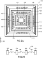
- micro-device 100 according to a second embodiment is shown schematically on the Figures 2A and 2B .
- the micro-device 100 represented on the Figures 2A and 2B comprise the fixed element 102 to which the first mobile element 104 is suspended by the first holding means 106.
- This micro-device 100 also comprises the second mobile element 108 forming the mobile mass of the micro-device 100 whose displacements are intended to be detected.
- the micro-device 100 comprises a third movable element 124 interposed between the first and second movable elements 104, 108.
- the second movable element 108 is disposed inside the space surrounded by the frame formed by the third movable element 124, and is suspended from the third mobile element 124 by the second holding means 110.
- the second movable element 108 can therefore move in one or more degrees of freedom with respect to the third movable element 124.
- the third movable element 124 is disposed within the space surrounded by the frame formed by the first movable element 104.
- the third movable element 124 is suspended from the first movable element 104 by third corresponding holding means 126. for example to micro-beams.
- These third holding means 126 are such that the third movable element 124 can move in one or more degrees of freedom with respect to the first movable element 104, and thus also with respect to the fixed element 102.
- the third movable element 124 can move in translation parallel to the axis X and parallel to the axis Y.
- other types of displacement of the third element mobile 124 relative to the first movable element 104 are possible: translation parallel to the axis X, rotation along at least one of the axes X, Y or Z, etc.
- the micro-device 100 comprises, in addition to the first interdigitated combs 112 present at the level inner faces of the frame formed by the fixed member 102 and at the outer faces of the frame formed by the first movable member 104, and second interdigital combs 114 present at the inner faces of the frame formed by the third movable member 124 and at the outer faces of the second movable element 108, third interdigital combs 128 present at the inner faces of the frame formed by the first movable element 104 and at the outer faces of the frame formed by the third movable element 124.
- These third combs interdigitals 114 ensure the detection of the movement in translation in the plane (X, Y) of the third element mo bile 124 relative to the first movable member 104.
- the micro-device 100 may comprise other means for detecting the displacements of the first mobile element 104 and / or the second mobile element 108 and / or the third mobile element 124, replacing or in addition to the combs interdigitals 112, 114 and 128.
- detection means are for example capacitive and / or piezoelectric and / or piezoresistive, etc.
- the second movable element 108 whose movement is intended to be detected is connected to the fixed element 102 by three successive suspension means 106, 126, 110 and independent from each other.
- this configuration further improves the insulation of the second mobile element 108 with respect to the vibrations, or more generally to the external mechanical disturbances experienced by the micro-device 100.
- the first movable element 104 is encapsulated within the first cavity 116 which can be hermetically sealed with respect to the external environment of the micro-device 100 and delimited by the substrate, the faces of the fixed element 102 (which form at least part of the side walls of this first cavity 116) and the first cover (not visible on the Figures 2A and 2B ) secured to the fixed element 102 by means of the first sealing bead 118.
- the third movable element 124 is encapsulated within the second cavity 120 which is here hermetically sealed with respect to the atmosphere prevailing within of the first cavity 116, or isolated vis-à-vis the first cavity 116, and defined by the substrate, the inner faces of the first movable member 104 (which form at least a portion of the side walls of the second cavity 120) and the second hood (not visible on Figures 2A and 2B ) secured to the first movable element 104 via the second sealing bead 122.
- the second sealing bead 122 and the second bonnet are, like the first movable element 104, movable relative to the fixed element 102.
- the second movable element 108 is encapsulated within a third cavity 130 which is for example hermetically closed, or more generally isolated, with respect to the atmospheres prevailing within the first and second recesses 116 and 120, and delimited by the substrate, the inner faces of the third movable member 124 (which form at least a portion of the side walls of this third cavity 130) and a third cover (not visible on the Figures 2A and 2B ) secured to the third movable member 124 via a third sealing bead 132.
- the third sealing bead 132 and the third bonnet are, like the third movable member 124, movable relative to the first movable member 104 as well as relative to the fixed element 102.
- the first movable element 104 can be encapsulated in an atmosphere different from that in which the second movable element 108 is encapsulated and that in which which is encapsulated the third movable element 124, that is to say in the presence of gas and / or different pressure.
- the micro-device 100 it is possible for the micro-device 100 to have more than two intermediate movable elements interposed, via separate suspension means, between the fixed element and the mobile element forming the mobile mass of the microstrip. device 100.
- the elements 102, 104 and 124 have sections, in the plane of the substrate on which the micro-device 100 is made, forming substantially square frames.
- the micro-device 100 shown on the figure 3 has elements 102 and 104 of shape, in the plane (X, Y) substantially parallel to the substrate, annular.
- the second movable element 108 has a shape, in the plane (X, Y), of disk.
- the cavities 116 and 120 thus have cylindrical shapes.
- the micro-device 100 represented on the figure 4 comprises elements 102 and 104 forming, in the plane (X, Y), rectangular frames.
- the second movable element 108 also has, in the plane (X, Y), a rectangular shape.
- the figure 5 represents another micro-device 100 in which, unlike the previous examples in which the second movable element 108 has a shape substantially corresponding to that of the cavity in which it is encapsulated, the second element 108 here has a shape different from that of the cavity 120 in which it is encapsulated.
- the second movable element 108 has a shape, in the plane (X, Y), having a hollow 134.
- the structure is symmetrical with respect to an axis parallel to the Y axis (in contrast to the structures previous embodiments which are symmetrical with respect to their center).
- the different cavities nested within each other within the micro-device 100 are concentric, that is to say have their center arranged one above the other.
- the centers of these cavities are offset relative to each other.
- the second cavity 120 is not centered with respect to the first cavity 116 because one side of the first movable member 104 is much larger than the other sides.
- the cavities 116 and 120 are not concentric because the cavity 116 does not have the same shape in the (X, Y) plane as the cavity 120.
- the different cavities of the same micro-device 100 can be closed simultaneously during a single closure step implemented collectively at the substrate scale.
- the different cavities of a same micro-device 100 can be closed simultaneously by the implementation of the same collective closure step at the substrate scale, the materials used to form the various sealing beads different cavities of the same micro-device 100 may be different from one sealing bead to another.
- the sealing beads it is possible to make a first portion of the cord on the face of the element on which a cover is intended to be secured, and a second portion of the cord on the face of the cover to be secured to one of the elements of the micro-device.
- first bonding material on the cover
- second bonding material on the fixed or movable member of the micro-device 100
- these first and second bonding materials may be similar or not .
- the sealing bead materials are advantageously metallic materials such as eutectic alloys.
- a sealing bead can be made from portions of Au-Si joined together to form the sealing bead. It is also possible that one portion of the cord has Au-Si and the other portion of the cord has Au-Sn.
- the covers are secured to the various fixed and movable elements of the micro-device 100 by means of sealing beads 118, 122 and 132.
- These sealing beads may comprise metallic materials when the covers are secured to the fixed and movable elements of the micro-device 100. It is also possible that these sealing beads comprise one or more non-metallic materials, for example one or more polymeric materials.
- a method of producing a micro-device 100 according to a particular embodiment is now described in connection with the Figures 8A to 8F .
- the micro-device 100 obtained by the implementation of this method corresponds to the micro-device 100 previously described in connection with the Figures 1A and 1B .
- the micro-device 100 is for example made from a first semiconductor-on-insulator substrate, for example SOI (silicon on insulator).
- This substrate visible on the figure 8A , comprises a support layer 136, a buried dielectric layer 138, or BOX ("Buried Oxide"), comprising, for example, semiconductor oxide such as SiO 2 , and a semiconductor surface layer 140 comprising, example of silicon.
- the total thickness of the layers 138 and 140 is for example between about 100 nm and 100 microns. Trenches 165 are made through the support layer 136.
- the layer 140 corresponds to a layer of material suitable for producing the various fixed and moving elements of the micro-device 100.
- the layer 138 corresponds to a layer of sacrificial material.
- the micro-device 100 may be made from a solid substrate 136, or bulk, comprising, for example, a semiconductor such as silicon, on which are deposited successively a sacrificial layer 138, for example a dielectric layer such as a semiconductor oxide layer, and a material layer 140 in which the mobile structures of the micro-device 100 will be made, for example corresponding to a semiconductor layer such as doped silicon or not, germanium doped or not, etc.
- the sacrificial layer 138 and the layer of material 140 may be formed using various techniques such as LPCVD (chemical vapor deposition) deposits, PECVD (plasma enhanced chemical vapor deposition), ALD ( atomic layer deposition), PVD (physical vapor deposition), or epitaxy, etc.
- LPCVD chemical vapor deposition
- PECVD plasma enhanced chemical vapor deposition
- ALD atomic layer deposition
- PVD physical vapor deposition
- epitaxy etc.
- a dielectric layer 142 is then formed on the surface layer 140.
- a layer of a first material of the sealing bead is then deposited on the dielectric layer 142.
- This first material is for example a metallic material, such as Au, Al or SnAg, or a semiconductor material such as Ge.
- This layer of the first material of the sealing bead is etched to form first portions of the various sealing beads that the micro-device 100 is intended to contain. On the example of the Figure 8B the layer is etched and the remaining portions of this layer retained on the dielectric layer 142 correspond to a first portion 118.1 of the first sealing bead 118 and a first portion 122.1 of the second bead 122.
- an etching is then carried out through the layers 142 and 140 in order to form, within the semiconductor layer 140, the various fixed and mobile elements of the micro-device 100 (the element 102 and the moving elements 104 and 108 on the example of the Figure 8C ) and the holding means by which the movable elements are intended to be suspended (micro-beams 106 and 110 on the example of the Figure 8C ), and also the detection and / or actuation elements of the micro-device 100 (interdigitated first and second interdigitated combs 112 and 114 in the example of FIG. Figure 8C ).
- the trenches etched through the layers 142 and 140 which delimit the different elements of the micro-device 100 also form the spaces which will then be used to release the various elements of the micro-device 100. If necessary, the etching implemented at this stage of the The method may also be used to provide additional release holes 144 through layers 142 and 140 if the trenches defining the different members of micro-device 100 are not sufficient for the subsequent release of these elements.
- release holes 144 are formed through the second movable member 108 so that the material of the layer 138 under the second movable member 108 can be properly etched.
- Etching of a part of the layer 138 is then carried out through the trenches and the possible release holes 144 made during the previous etching step, in order to release the mobile elements 108 and 104 of the micro-device 100 ( see figure 8D ). Portions of layer 138 are kept under the movable element 104. The mobility of the movable element 104 relative to the fixed part 102 is provided by the trenches 165.
- a second substrate 146 is then transferred to the previously formed structure to form the covers of the cavities in which the mobile elements 104 and 108 of the micro-device 100 are encapsulated.
- said second substrate 146 corresponds to a semiconductor-on-insulator substrate such as an SOI substrate comprising a support layer 148, a buried dielectric layer 150 and a semiconductor surface layer 152 comprising, for example, silicon.
- the second substrate 146 is here secured to the various fixed and movable elements of the micro-device 100 via the implementation of a metal seal.
- second portions 118.2 and 122.2 of the sealing beads 118, 122 are formed beforehand on the surface layer 152, then these second portions 118.2 and 122.2 of the sealing beads 118, 122 are brought into contact with the first portions 118.1 and 122.1 of the sealing beads 118, 122, and annealing completes the formation of the sealing beads 118 and 122.
- the sealing beads 118, 122 are for example formed by first portions 118.1 and 122.1 comprising Au and the second portions 118.2 and 118.2. 122.2 comprising Si or Au or Sn, or first portions 118.1 and 122.1 comprising Al and second portions 118.2 and 122.2 comprising Ge.
- the second substrate 146 could be secured to the assembly previously made via the implementation of a direct sealing, or direct bonding, for example silicon against silicon, or dielectric against dielectric, or dielectric against silicon, etc.
- cords of one or more non-metallic materials for example polymers, could be formed between the second substrate 146 and the structure previously made comprising the different elements of the micro-device 100.
- release holes 154 pass through the support layer 148 and form accesses to the buried dielectric layer 150. These release holes 154 are temporarily plugged via a dielectric layer 156 covering the face of the support layer 148 opposite to that against which the buried dielectric layer 150 is located.
- the surface layer 152 is structured so as to form different parts intended to form part of the various hoods of the cavities in which the various mobile parts of the micro-device 100 are encapsulated. So, on the example of the figure 8E a first portion 158 of the surface layer 152, which is fixed with respect to the fixed member 102, forms, with the support layer 148, the first cover of the first cavity 116. A second portion 160 of the surface layer 152 is movable relative to the first portion 158 by means 161 for holding in suspension, for example micro-beam type arms, this second portion 160 relative to the first portion 158. This second portion 160 of the surface layer 152 forms the second hood of the second cavity 120.
- At least one opening 155 (represented in dashed line on the figure 8E ) is carried out through the support layer 136 in order to communicate the interior of the second cavity 120 with the external atmosphere in which the micro-device 100 is located.
- the pressure within the second cavity 120 corresponds to at the pressure outside the micro-device 100.
- the micro-device 100 is completed by etching the dielectric layer 156 and the portions of the buried dielectric layer 150 accessible via the release holes 154, thereby releasing the second portion 160 of the surface layer 152 from the diaper support 148 and thus making the second hood mobile with respect to the first hood ( figure 8F ). Due to the unblocked release holes 154, the pressure within the first cavity 116 corresponds to the pressure outside the micro-device 100.
- the buried dielectric layer 150 is selectively removed from the support layer 148 and the semiconductor surface layer 152 to provide mobility for the second portion 160 of the the surface layer 152, which is intended to form the second cover of the second cavity 120, with respect to the first portion 158 of this layer 152 intended to form part of the side walls of the first cavity 116.
- a portion or layer of getter material 164 may be disposed against the second portion 160 of the surface layer 152 so that after the transfer of the second substrate 146, the portion of getter material 164 is encapsulated in the second cavity 120.
- the temperature at which sealing of the second substrate 146 is performed, as well as the nature of the getter material used for the portion 164 may advantageously be chosen such that the getter material of the portion 164 is activated thermally during this sealing, that is to say such that the thermal activation temperature of the getter material is less than or equal to that of the temperature at which the sealing is implemented.
- the second substrate 146 is then transferred and sealed to the structure previously made, completing the production of the micro-device 100.
- the micro-device 100 obtained is represented on the figure 9 .
- the pressure difference prevailing in the first and second cavities 116, 120 is not due to the fact that the pressure in the first cavity 116 is equal to the atmospheric pressure obtained by means of holes through the layer 148, but thanks to the absorption and / or gas adsorption carried out by the portion of getter material 164 in the second cavity 120.
Landscapes
- Engineering & Computer Science (AREA)
- Microelectronics & Electronic Packaging (AREA)
- Computer Hardware Design (AREA)
- Manufacturing & Machinery (AREA)
- Micromachines (AREA)
- Gyroscopes (AREA)
Applications Claiming Priority (1)
| Application Number | Priority Date | Filing Date | Title |
|---|---|---|---|
| FR1752157A FR3063991B1 (fr) | 2017-03-16 | 2017-03-16 | Micro-dispositif a plusieurs elements mobiles disposes au sein de plusieurs cavites imbriquees |
Publications (2)
| Publication Number | Publication Date |
|---|---|
| EP3375753A1 true EP3375753A1 (de) | 2018-09-19 |
| EP3375753B1 EP3375753B1 (de) | 2020-12-09 |
Family
ID=59381378
Family Applications (1)
| Application Number | Title | Priority Date | Filing Date |
|---|---|---|---|
| EP18161932.1A Active EP3375753B1 (de) | 2017-03-16 | 2018-03-15 | Mikrovorrichtung mit mehreren beweglichen elementen, die im inneren von mehreren eingebetteten hohlräumen angeordnet sind |
Country Status (3)
| Country | Link |
|---|---|
| US (1) | US10472227B2 (de) |
| EP (1) | EP3375753B1 (de) |
| FR (1) | FR3063991B1 (de) |
Families Citing this family (1)
| Publication number | Priority date | Publication date | Assignee | Title |
|---|---|---|---|---|
| FR3063992B1 (fr) | 2017-03-16 | 2021-07-16 | Commissariat Energie Atomique | Micro-dispositif comprenant au moins un element mobile |
Citations (2)
| Publication number | Priority date | Publication date | Assignee | Title |
|---|---|---|---|---|
| US20060284514A1 (en) * | 2005-06-15 | 2006-12-21 | Samsung Electronics Co., Ltd. | Actuator having vertical comb electrode structure |
| US20120230079A1 (en) * | 2011-03-08 | 2012-09-13 | Kabushiki Kaisha Toshiba | Actuator and storage device |
Family Cites Families (10)
| Publication number | Priority date | Publication date | Assignee | Title |
|---|---|---|---|---|
| JP3003429B2 (ja) * | 1992-10-08 | 2000-01-31 | 富士電機株式会社 | ねじり振動子および光偏向子 |
| JP2005088188A (ja) * | 2003-08-12 | 2005-04-07 | Fujitsu Ltd | マイクロ揺動素子およびマイクロ揺動素子駆動方法 |
| US7247246B2 (en) * | 2003-10-20 | 2007-07-24 | Atmel Corporation | Vertical integration of a MEMS structure with electronics in a hermetically sealed cavity |
| DE102004027501A1 (de) | 2004-06-04 | 2005-12-22 | Robert Bosch Gmbh | Mikromechanisches Bauelement mit mehreren Kavernen und Herstellungsverfahren |
| US7442570B2 (en) | 2005-03-18 | 2008-10-28 | Invensence Inc. | Method of fabrication of a AL/GE bonding in a wafer packaging environment and a product produced therefrom |
| DE102006016260A1 (de) | 2006-04-06 | 2007-10-18 | Fraunhofer-Gesellschaft zur Förderung der angewandten Forschung e.V. | Mikromechanische Gehäusung mit mindestens zwei Kavitäten mit unterschiedlichem Innendruck und/oder unterschiedlicher Gaszusammensetzung sowie Verfahren zu deren Herstellung |
| JP5541306B2 (ja) * | 2011-05-27 | 2014-07-09 | 株式会社デンソー | 力学量センサ装置およびその製造方法 |
| US20130127879A1 (en) * | 2011-11-18 | 2013-05-23 | Qualcomm Mems Technologies, Inc. | Glass-encapsulated pressure sensor |
| JP2017147363A (ja) * | 2016-02-18 | 2017-08-24 | 株式会社東芝 | Mems装置 |
| ITUA20163571A1 (it) * | 2016-05-18 | 2017-11-18 | St Microelectronics Srl | Trasduttore acustico mems con elettrodi interdigitati e relativo procedimento di fabbricazione |
-
2017
- 2017-03-16 FR FR1752157A patent/FR3063991B1/fr not_active Expired - Fee Related
-
2018
- 2018-03-12 US US15/918,008 patent/US10472227B2/en active Active
- 2018-03-15 EP EP18161932.1A patent/EP3375753B1/de active Active
Patent Citations (2)
| Publication number | Priority date | Publication date | Assignee | Title |
|---|---|---|---|---|
| US20060284514A1 (en) * | 2005-06-15 | 2006-12-21 | Samsung Electronics Co., Ltd. | Actuator having vertical comb electrode structure |
| US20120230079A1 (en) * | 2011-03-08 | 2012-09-13 | Kabushiki Kaisha Toshiba | Actuator and storage device |
Also Published As
| Publication number | Publication date |
|---|---|
| EP3375753B1 (de) | 2020-12-09 |
| US10472227B2 (en) | 2019-11-12 |
| FR3063991B1 (fr) | 2019-05-03 |
| US20180265348A1 (en) | 2018-09-20 |
| FR3063991A1 (fr) | 2018-09-21 |
Similar Documents
| Publication | Publication Date | Title |
|---|---|---|
| EP2546189B1 (de) | Verfahren zur Herstellung einer Struktur mit einer vergrabenen Elektrode durch direkte Übertragung | |
| Stark et al. | A low-temperature thin-film electroplated metal vacuum package | |
| EP2921836A1 (de) | Sensor zum Messen des mikroelektromechanischen und/oder nanoelektromechanischen Differentialdrucks | |
| FR2898683A1 (fr) | Accelerometre triaxial a membrane | |
| EP2450949B1 (de) | Einkapselungssstruktur einer Mikrovorrichtung, die ein Getter-Material umfasst | |
| CA2866388C (fr) | Procede de fabrication d'un capteur de pression et capteur correspondant | |
| EP2215006A2 (de) | Vorrichtung mit integrierter schaltung und n/mems sowie herstellungsverfahren | |
| EP2546188B1 (de) | Verfahren zur Herstellung einer Struktur mit einer aufgehängten Membran und einer vergrabenen Elektrode | |
| EP2520900B1 (de) | Gyroskop mit reduzierter parasitärer Kapazität | |
| EP3538479B1 (de) | Vorrichtung zur übertragung einer bewegung und einer kraft zwischen zwei voneinander isolierten zonen | |
| EP3257808B1 (de) | Mikroelektromechanische und/oder nanoelektromechanische vorrichtung mit bewegung ausserhalb der ebene, die mit kapazitiven mitteln zur änderung der oberfläche ausgestattet ist | |
| EP3020684B1 (de) | Einkapselungsstruktur mit hohlraum der an einen aus einem durchlässigen material gebildeten gasinjektionskanal gekoppelt ist | |
| Rahman et al. | Device-level vacuum packaging for RF MEMS | |
| EP3375753B1 (de) | Mikrovorrichtung mit mehreren beweglichen elementen, die im inneren von mehreren eingebetteten hohlräumen angeordnet sind | |
| FR3057261A1 (fr) | Capteur micromecanique et son procede de fabrication | |
| EP3042509B1 (de) | Digitale akustische vorrichtung mit erhöhter tonleistung | |
| EP3217181B1 (de) | Gedämpfter linearer beschleunigungsmesser | |
| EP3159302A1 (de) | Einkapselungsverfahren eines mikroelektronischen bauteils | |
| FR3028257A1 (fr) | Procede de fabrication d'un dispositif electromecanique et dispositif correspondant | |
| Candler et al. | Encapsulation by film deposition | |
| FR3075772A1 (fr) | Mise en œuvre d'une structure de decouplage pour l'assemblage d'un composant avec un boitier | |
| EP3596003A1 (de) | Mikrovorrichtung mit mindestens zwei beweglichen elementen | |
| FR3074358A1 (fr) | Procede de realisation d'une cavite etanche a couche mince | |
| EP1572575B1 (de) | Verkapselte mikrostruktur und deren herstellungsverfahren | |
| Liu et al. | UMEMS: A Robust Technology Platform For Quality Automotive Inertial Sensor Manufacturing |
Legal Events
| Date | Code | Title | Description |
|---|---|---|---|
| PUAI | Public reference made under article 153(3) epc to a published international application that has entered the european phase |
Free format text: ORIGINAL CODE: 0009012 |
|
| STAA | Information on the status of an ep patent application or granted ep patent |
Free format text: STATUS: REQUEST FOR EXAMINATION WAS MADE |
|
| 17P | Request for examination filed |
Effective date: 20180315 |
|
| AK | Designated contracting states |
Kind code of ref document: A1 Designated state(s): AL AT BE BG CH CY CZ DE DK EE ES FI FR GB GR HR HU IE IS IT LI LT LU LV MC MK MT NL NO PL PT RO RS SE SI SK SM TR |
|
| AX | Request for extension of the european patent |
Extension state: BA ME |
|
| STAA | Information on the status of an ep patent application or granted ep patent |
Free format text: STATUS: EXAMINATION IS IN PROGRESS |
|
| 17Q | First examination report despatched |
Effective date: 20190502 |
|
| RAP1 | Party data changed (applicant data changed or rights of an application transferred) |
Owner name: COMMISSARIAT A L'ENERGIE ATOMIQUE ET AUX ENERGIES Owner name: SAFRAN |
|
| GRAP | Despatch of communication of intention to grant a patent |
Free format text: ORIGINAL CODE: EPIDOSNIGR1 |
|
| STAA | Information on the status of an ep patent application or granted ep patent |
Free format text: STATUS: GRANT OF PATENT IS INTENDED |
|
| INTG | Intention to grant announced |
Effective date: 20200703 |
|
| GRAS | Grant fee paid |
Free format text: ORIGINAL CODE: EPIDOSNIGR3 |
|
| GRAA | (expected) grant |
Free format text: ORIGINAL CODE: 0009210 |
|
| STAA | Information on the status of an ep patent application or granted ep patent |
Free format text: STATUS: THE PATENT HAS BEEN GRANTED |
|
| AK | Designated contracting states |
Kind code of ref document: B1 Designated state(s): AL AT BE BG CH CY CZ DE DK EE ES FI FR GB GR HR HU IE IS IT LI LT LU LV MC MK MT NL NO PL PT RO RS SE SI SK SM TR |
|
| REG | Reference to a national code |
Ref country code: GB Ref legal event code: FG4D Free format text: NOT ENGLISH |
|
| REG | Reference to a national code |
Ref country code: AT Ref legal event code: REF Ref document number: 1343251 Country of ref document: AT Kind code of ref document: T Effective date: 20201215 Ref country code: CH Ref legal event code: EP |
|
| REG | Reference to a national code |
Ref country code: DE Ref legal event code: R096 Ref document number: 602018010513 Country of ref document: DE |
|
| REG | Reference to a national code |
Ref country code: IE Ref legal event code: FG4D Free format text: LANGUAGE OF EP DOCUMENT: FRENCH |
|
| PG25 | Lapsed in a contracting state [announced via postgrant information from national office to epo] |
Ref country code: FI Free format text: LAPSE BECAUSE OF FAILURE TO SUBMIT A TRANSLATION OF THE DESCRIPTION OR TO PAY THE FEE WITHIN THE PRESCRIBED TIME-LIMIT Effective date: 20201209 Ref country code: RS Free format text: LAPSE BECAUSE OF FAILURE TO SUBMIT A TRANSLATION OF THE DESCRIPTION OR TO PAY THE FEE WITHIN THE PRESCRIBED TIME-LIMIT Effective date: 20201209 Ref country code: GR Free format text: LAPSE BECAUSE OF FAILURE TO SUBMIT A TRANSLATION OF THE DESCRIPTION OR TO PAY THE FEE WITHIN THE PRESCRIBED TIME-LIMIT Effective date: 20210310 Ref country code: NO Free format text: LAPSE BECAUSE OF FAILURE TO SUBMIT A TRANSLATION OF THE DESCRIPTION OR TO PAY THE FEE WITHIN THE PRESCRIBED TIME-LIMIT Effective date: 20210309 |
|
| REG | Reference to a national code |
Ref country code: AT Ref legal event code: MK05 Ref document number: 1343251 Country of ref document: AT Kind code of ref document: T Effective date: 20201209 |
|
| PG25 | Lapsed in a contracting state [announced via postgrant information from national office to epo] |
Ref country code: SE Free format text: LAPSE BECAUSE OF FAILURE TO SUBMIT A TRANSLATION OF THE DESCRIPTION OR TO PAY THE FEE WITHIN THE PRESCRIBED TIME-LIMIT Effective date: 20201209 Ref country code: LV Free format text: LAPSE BECAUSE OF FAILURE TO SUBMIT A TRANSLATION OF THE DESCRIPTION OR TO PAY THE FEE WITHIN THE PRESCRIBED TIME-LIMIT Effective date: 20201209 Ref country code: BG Free format text: LAPSE BECAUSE OF FAILURE TO SUBMIT A TRANSLATION OF THE DESCRIPTION OR TO PAY THE FEE WITHIN THE PRESCRIBED TIME-LIMIT Effective date: 20210309 |
|
| PGFP | Annual fee paid to national office [announced via postgrant information from national office to epo] |
Ref country code: DE Payment date: 20210310 Year of fee payment: 4 |
|
| REG | Reference to a national code |
Ref country code: NL Ref legal event code: MP Effective date: 20201209 |
|
| PG25 | Lapsed in a contracting state [announced via postgrant information from national office to epo] |
Ref country code: NL Free format text: LAPSE BECAUSE OF FAILURE TO SUBMIT A TRANSLATION OF THE DESCRIPTION OR TO PAY THE FEE WITHIN THE PRESCRIBED TIME-LIMIT Effective date: 20201209 Ref country code: HR Free format text: LAPSE BECAUSE OF FAILURE TO SUBMIT A TRANSLATION OF THE DESCRIPTION OR TO PAY THE FEE WITHIN THE PRESCRIBED TIME-LIMIT Effective date: 20201209 |
|
| REG | Reference to a national code |
Ref country code: LT Ref legal event code: MG9D |
|
| PG25 | Lapsed in a contracting state [announced via postgrant information from national office to epo] |
Ref country code: LT Free format text: LAPSE BECAUSE OF FAILURE TO SUBMIT A TRANSLATION OF THE DESCRIPTION OR TO PAY THE FEE WITHIN THE PRESCRIBED TIME-LIMIT Effective date: 20201209 Ref country code: EE Free format text: LAPSE BECAUSE OF FAILURE TO SUBMIT A TRANSLATION OF THE DESCRIPTION OR TO PAY THE FEE WITHIN THE PRESCRIBED TIME-LIMIT Effective date: 20201209 Ref country code: CZ Free format text: LAPSE BECAUSE OF FAILURE TO SUBMIT A TRANSLATION OF THE DESCRIPTION OR TO PAY THE FEE WITHIN THE PRESCRIBED TIME-LIMIT Effective date: 20201209 Ref country code: SM Free format text: LAPSE BECAUSE OF FAILURE TO SUBMIT A TRANSLATION OF THE DESCRIPTION OR TO PAY THE FEE WITHIN THE PRESCRIBED TIME-LIMIT Effective date: 20201209 Ref country code: RO Free format text: LAPSE BECAUSE OF FAILURE TO SUBMIT A TRANSLATION OF THE DESCRIPTION OR TO PAY THE FEE WITHIN THE PRESCRIBED TIME-LIMIT Effective date: 20201209 Ref country code: PT Free format text: LAPSE BECAUSE OF FAILURE TO SUBMIT A TRANSLATION OF THE DESCRIPTION OR TO PAY THE FEE WITHIN THE PRESCRIBED TIME-LIMIT Effective date: 20210409 Ref country code: SK Free format text: LAPSE BECAUSE OF FAILURE TO SUBMIT A TRANSLATION OF THE DESCRIPTION OR TO PAY THE FEE WITHIN THE PRESCRIBED TIME-LIMIT Effective date: 20201209 |
|
| PG25 | Lapsed in a contracting state [announced via postgrant information from national office to epo] |
Ref country code: AT Free format text: LAPSE BECAUSE OF FAILURE TO SUBMIT A TRANSLATION OF THE DESCRIPTION OR TO PAY THE FEE WITHIN THE PRESCRIBED TIME-LIMIT Effective date: 20201209 Ref country code: PL Free format text: LAPSE BECAUSE OF FAILURE TO SUBMIT A TRANSLATION OF THE DESCRIPTION OR TO PAY THE FEE WITHIN THE PRESCRIBED TIME-LIMIT Effective date: 20201209 |
|
| REG | Reference to a national code |
Ref country code: DE Ref legal event code: R097 Ref document number: 602018010513 Country of ref document: DE |
|
| PG25 | Lapsed in a contracting state [announced via postgrant information from national office to epo] |
Ref country code: IS Free format text: LAPSE BECAUSE OF FAILURE TO SUBMIT A TRANSLATION OF THE DESCRIPTION OR TO PAY THE FEE WITHIN THE PRESCRIBED TIME-LIMIT Effective date: 20210409 |
|
| PLBE | No opposition filed within time limit |
Free format text: ORIGINAL CODE: 0009261 |
|
| STAA | Information on the status of an ep patent application or granted ep patent |
Free format text: STATUS: NO OPPOSITION FILED WITHIN TIME LIMIT |
|
| PG25 | Lapsed in a contracting state [announced via postgrant information from national office to epo] |
Ref country code: AL Free format text: LAPSE BECAUSE OF FAILURE TO SUBMIT A TRANSLATION OF THE DESCRIPTION OR TO PAY THE FEE WITHIN THE PRESCRIBED TIME-LIMIT Effective date: 20201209 Ref country code: MC Free format text: LAPSE BECAUSE OF FAILURE TO SUBMIT A TRANSLATION OF THE DESCRIPTION OR TO PAY THE FEE WITHIN THE PRESCRIBED TIME-LIMIT Effective date: 20201209 Ref country code: IT Free format text: LAPSE BECAUSE OF FAILURE TO SUBMIT A TRANSLATION OF THE DESCRIPTION OR TO PAY THE FEE WITHIN THE PRESCRIBED TIME-LIMIT Effective date: 20201209 |
|
| REG | Reference to a national code |
Ref country code: CH Ref legal event code: PL |
|
| 26N | No opposition filed |
Effective date: 20210910 |
|
| PG25 | Lapsed in a contracting state [announced via postgrant information from national office to epo] |
Ref country code: DK Free format text: LAPSE BECAUSE OF FAILURE TO SUBMIT A TRANSLATION OF THE DESCRIPTION OR TO PAY THE FEE WITHIN THE PRESCRIBED TIME-LIMIT Effective date: 20201209 Ref country code: SI Free format text: LAPSE BECAUSE OF FAILURE TO SUBMIT A TRANSLATION OF THE DESCRIPTION OR TO PAY THE FEE WITHIN THE PRESCRIBED TIME-LIMIT Effective date: 20201209 |
|
| REG | Reference to a national code |
Ref country code: BE Ref legal event code: MM Effective date: 20210331 |
|
| PG25 | Lapsed in a contracting state [announced via postgrant information from national office to epo] |
Ref country code: CH Free format text: LAPSE BECAUSE OF NON-PAYMENT OF DUE FEES Effective date: 20210331 Ref country code: IE Free format text: LAPSE BECAUSE OF NON-PAYMENT OF DUE FEES Effective date: 20210315 Ref country code: LI Free format text: LAPSE BECAUSE OF NON-PAYMENT OF DUE FEES Effective date: 20210331 Ref country code: LU Free format text: LAPSE BECAUSE OF NON-PAYMENT OF DUE FEES Effective date: 20210315 Ref country code: ES Free format text: LAPSE BECAUSE OF FAILURE TO SUBMIT A TRANSLATION OF THE DESCRIPTION OR TO PAY THE FEE WITHIN THE PRESCRIBED TIME-LIMIT Effective date: 20201209 |
|
| PG25 | Lapsed in a contracting state [announced via postgrant information from national office to epo] |
Ref country code: IS Free format text: LAPSE BECAUSE OF FAILURE TO SUBMIT A TRANSLATION OF THE DESCRIPTION OR TO PAY THE FEE WITHIN THE PRESCRIBED TIME-LIMIT Effective date: 20210409 |
|
| PG25 | Lapsed in a contracting state [announced via postgrant information from national office to epo] |
Ref country code: BE Free format text: LAPSE BECAUSE OF NON-PAYMENT OF DUE FEES Effective date: 20210331 |
|
| REG | Reference to a national code |
Ref country code: DE Ref legal event code: R119 Ref document number: 602018010513 Country of ref document: DE |
|
| GBPC | Gb: european patent ceased through non-payment of renewal fee |
Effective date: 20220315 |
|
| PG25 | Lapsed in a contracting state [announced via postgrant information from national office to epo] |
Ref country code: GB Free format text: LAPSE BECAUSE OF NON-PAYMENT OF DUE FEES Effective date: 20220315 Ref country code: FR Free format text: LAPSE BECAUSE OF NON-PAYMENT OF DUE FEES Effective date: 20220331 Ref country code: DE Free format text: LAPSE BECAUSE OF NON-PAYMENT OF DUE FEES Effective date: 20221001 |
|
| REG | Reference to a national code |
Ref country code: GB Ref legal event code: S28 Free format text: APPLICATION FILED |
|
| PG25 | Lapsed in a contracting state [announced via postgrant information from national office to epo] |
Ref country code: FR Free format text: LAPSE BECAUSE OF NON-PAYMENT OF DUE FEES Effective date: 20220331 |
|
| PGFP | Annual fee paid to national office [announced via postgrant information from national office to epo] |
Ref country code: FR Payment date: 20230320 Year of fee payment: 6 |
|
| PGRI | Patent reinstated in contracting state [announced from national office to epo] |
Ref country code: FR Effective date: 20230309 |
|
| REG | Reference to a national code |
Ref country code: GB Ref legal event code: 732E Free format text: REGISTERED BETWEEN 20230504 AND 20230510 |
|
| PG25 | Lapsed in a contracting state [announced via postgrant information from national office to epo] |
Ref country code: CY Free format text: LAPSE BECAUSE OF FAILURE TO SUBMIT A TRANSLATION OF THE DESCRIPTION OR TO PAY THE FEE WITHIN THE PRESCRIBED TIME-LIMIT Effective date: 20201209 |
|
| REG | Reference to a national code |
Ref country code: GB Ref legal event code: S28 Free format text: RESTORATION ALLOWED Effective date: 20230621 |
|
| PG25 | Lapsed in a contracting state [announced via postgrant information from national office to epo] |
Ref country code: HU Free format text: LAPSE BECAUSE OF FAILURE TO SUBMIT A TRANSLATION OF THE DESCRIPTION OR TO PAY THE FEE WITHIN THE PRESCRIBED TIME-LIMIT; INVALID AB INITIO Effective date: 20180315 |
|
| PG25 | Lapsed in a contracting state [announced via postgrant information from national office to epo] |
Ref country code: MK Free format text: LAPSE BECAUSE OF FAILURE TO SUBMIT A TRANSLATION OF THE DESCRIPTION OR TO PAY THE FEE WITHIN THE PRESCRIBED TIME-LIMIT Effective date: 20201209 |
|
| PGFP | Annual fee paid to national office [announced via postgrant information from national office to epo] |
Ref country code: GB Payment date: 20240220 Year of fee payment: 7 |