EP3374757B1 - Sels-nanofinger-seitenwand-beschichtungsschicht - Google Patents
Sels-nanofinger-seitenwand-beschichtungsschicht Download PDFInfo
- Publication number
- EP3374757B1 EP3374757B1 EP16899646.0A EP16899646A EP3374757B1 EP 3374757 B1 EP3374757 B1 EP 3374757B1 EP 16899646 A EP16899646 A EP 16899646A EP 3374757 B1 EP3374757 B1 EP 3374757B1
- Authority
- EP
- European Patent Office
- Prior art keywords
- coating layer
- polymer
- sensor
- pillars
- substrate
- Prior art date
- Legal status (The legal status is an assumption and is not a legal conclusion. Google has not performed a legal analysis and makes no representation as to the accuracy of the status listed.)
- Active
Links
- 239000011247 coating layer Substances 0.000 title claims description 102
- 239000000758 substrate Substances 0.000 claims description 55
- 229910052751 metal Inorganic materials 0.000 claims description 51
- 239000002184 metal Substances 0.000 claims description 51
- 239000000463 material Substances 0.000 claims description 45
- 229920000642 polymer Polymers 0.000 claims description 39
- 238000000034 method Methods 0.000 claims description 37
- VYPSYNLAJGMNEJ-UHFFFAOYSA-N Silicium dioxide Chemical compound O=[Si]=O VYPSYNLAJGMNEJ-UHFFFAOYSA-N 0.000 claims description 14
- 239000011248 coating agent Substances 0.000 claims description 11
- 238000000576 coating method Methods 0.000 claims description 11
- 239000002861 polymer material Substances 0.000 claims description 8
- 238000000623 plasma-assisted chemical vapour deposition Methods 0.000 claims description 7
- -1 polytetrafluoroethylene Polymers 0.000 claims description 7
- 239000000377 silicon dioxide Substances 0.000 claims description 6
- 238000004020 luminiscence type Methods 0.000 claims description 5
- 229910052681 coesite Inorganic materials 0.000 claims description 4
- 229910052906 cristobalite Inorganic materials 0.000 claims description 4
- 229910052682 stishovite Inorganic materials 0.000 claims description 4
- 229910052905 tridymite Inorganic materials 0.000 claims description 4
- PCHJSUWPFVWCPO-UHFFFAOYSA-N gold Chemical compound [Au] PCHJSUWPFVWCPO-UHFFFAOYSA-N 0.000 claims description 3
- 229910052737 gold Inorganic materials 0.000 claims description 3
- 239000010931 gold Substances 0.000 claims description 3
- 229920001343 polytetrafluoroethylene Polymers 0.000 claims description 3
- 239000004810 polytetrafluoroethylene Substances 0.000 claims description 3
- 229910052709 silver Inorganic materials 0.000 claims description 3
- 239000004332 silver Substances 0.000 claims description 3
- 229910045601 alloy Inorganic materials 0.000 claims description 2
- 239000000956 alloy Substances 0.000 claims description 2
- 229910052802 copper Inorganic materials 0.000 claims description 2
- 239000010949 copper Substances 0.000 claims description 2
- 229920002120 photoresistant polymer Polymers 0.000 claims description 2
- 229910052697 platinum Inorganic materials 0.000 claims description 2
- PPBRXRYQALVLMV-UHFFFAOYSA-N Styrene Chemical compound C=CC1=CC=CC=C1 PPBRXRYQALVLMV-UHFFFAOYSA-N 0.000 claims 2
- OEPOKWHJYJXUGD-UHFFFAOYSA-N 2-(3-phenylmethoxyphenyl)-1,3-thiazole-4-carbaldehyde Chemical compound O=CC1=CSC(C=2C=C(OCC=3C=CC=CC=3)C=CC=2)=N1 OEPOKWHJYJXUGD-UHFFFAOYSA-N 0.000 claims 1
- NLHHRLWOUZZQLW-UHFFFAOYSA-N Acrylonitrile Chemical compound C=CC#N NLHHRLWOUZZQLW-UHFFFAOYSA-N 0.000 claims 1
- CERQOIWHTDAKMF-UHFFFAOYSA-M Methacrylate Chemical compound CC(=C)C([O-])=O CERQOIWHTDAKMF-UHFFFAOYSA-M 0.000 claims 1
- XTXRWKRVRITETP-UHFFFAOYSA-N Vinyl acetate Chemical compound CC(=O)OC=C XTXRWKRVRITETP-UHFFFAOYSA-N 0.000 claims 1
- 229910052738 indium Inorganic materials 0.000 claims 1
- 229910052703 rhodium Inorganic materials 0.000 claims 1
- BFKJFAAPBSQJPD-UHFFFAOYSA-N tetrafluoroethene Chemical group FC(F)=C(F)F BFKJFAAPBSQJPD-UHFFFAOYSA-N 0.000 claims 1
- 239000010410 layer Substances 0.000 description 23
- 239000012491 analyte Substances 0.000 description 16
- 239000011229 interlayer Substances 0.000 description 9
- 230000008569 process Effects 0.000 description 8
- XUIMIQQOPSSXEZ-UHFFFAOYSA-N Silicon Chemical compound [Si] XUIMIQQOPSSXEZ-UHFFFAOYSA-N 0.000 description 5
- GWEVSGVZZGPLCZ-UHFFFAOYSA-N Titan oxide Chemical compound O=[Ti]=O GWEVSGVZZGPLCZ-UHFFFAOYSA-N 0.000 description 5
- 238000000231 atomic layer deposition Methods 0.000 description 5
- 239000003989 dielectric material Substances 0.000 description 5
- 239000006193 liquid solution Substances 0.000 description 5
- 229910052710 silicon Inorganic materials 0.000 description 5
- 239000010703 silicon Substances 0.000 description 5
- 229910052581 Si3N4 Inorganic materials 0.000 description 4
- XLOMVQKBTHCTTD-UHFFFAOYSA-N Zinc monoxide Chemical compound [Zn]=O XLOMVQKBTHCTTD-UHFFFAOYSA-N 0.000 description 4
- 239000012790 adhesive layer Substances 0.000 description 4
- 238000005452 bending Methods 0.000 description 4
- 238000010586 diagram Methods 0.000 description 4
- 238000005240 physical vapour deposition Methods 0.000 description 4
- 235000012239 silicon dioxide Nutrition 0.000 description 4
- HQVNEWCFYHHQES-UHFFFAOYSA-N silicon nitride Chemical compound N12[Si]34N5[Si]62N3[Si]51N64 HQVNEWCFYHHQES-UHFFFAOYSA-N 0.000 description 4
- 239000000126 substance Substances 0.000 description 4
- 230000015572 biosynthetic process Effects 0.000 description 3
- 239000011521 glass Substances 0.000 description 3
- 230000003993 interaction Effects 0.000 description 3
- 239000002086 nanomaterial Substances 0.000 description 3
- TWNQGVIAIRXVLR-UHFFFAOYSA-N oxo(oxoalumanyloxy)alumane Chemical compound O=[Al]O[Al]=O TWNQGVIAIRXVLR-UHFFFAOYSA-N 0.000 description 3
- 230000004044 response Effects 0.000 description 3
- 230000000717 retained effect Effects 0.000 description 3
- 239000002904 solvent Substances 0.000 description 3
- OKTJSMMVPCPJKN-UHFFFAOYSA-N Carbon Chemical compound [C] OKTJSMMVPCPJKN-UHFFFAOYSA-N 0.000 description 2
- LFQSCWFLJHTTHZ-UHFFFAOYSA-N Ethanol Chemical compound CCO LFQSCWFLJHTTHZ-UHFFFAOYSA-N 0.000 description 2
- BOTDANWDWHJENH-UHFFFAOYSA-N Tetraethyl orthosilicate Chemical compound CCO[Si](OCC)(OCC)OCC BOTDANWDWHJENH-UHFFFAOYSA-N 0.000 description 2
- 229910052799 carbon Inorganic materials 0.000 description 2
- 238000005229 chemical vapour deposition Methods 0.000 description 2
- 150000001875 compounds Chemical class 0.000 description 2
- 239000000356 contaminant Substances 0.000 description 2
- 238000011109 contamination Methods 0.000 description 2
- 230000007423 decrease Effects 0.000 description 2
- 238000000151 deposition Methods 0.000 description 2
- 239000010432 diamond Substances 0.000 description 2
- 229910003460 diamond Inorganic materials 0.000 description 2
- 230000005670 electromagnetic radiation Effects 0.000 description 2
- 238000005516 engineering process Methods 0.000 description 2
- 230000008020 evaporation Effects 0.000 description 2
- 238000001704 evaporation Methods 0.000 description 2
- 229910010272 inorganic material Inorganic materials 0.000 description 2
- 239000011147 inorganic material Substances 0.000 description 2
- 239000007788 liquid Substances 0.000 description 2
- 238000004519 manufacturing process Methods 0.000 description 2
- 239000007769 metal material Substances 0.000 description 2
- 238000000465 moulding Methods 0.000 description 2
- 238000002161 passivation Methods 0.000 description 2
- 239000004033 plastic Substances 0.000 description 2
- 229920003023 plastic Polymers 0.000 description 2
- BASFCYQUMIYNBI-UHFFFAOYSA-N platinum Chemical compound [Pt] BASFCYQUMIYNBI-UHFFFAOYSA-N 0.000 description 2
- 229920000139 polyethylene terephthalate Polymers 0.000 description 2
- 239000005020 polyethylene terephthalate Substances 0.000 description 2
- 229920001296 polysiloxane Polymers 0.000 description 2
- 239000010453 quartz Substances 0.000 description 2
- 229910052594 sapphire Inorganic materials 0.000 description 2
- 239000010980 sapphire Substances 0.000 description 2
- 239000002356 single layer Substances 0.000 description 2
- 238000004611 spectroscopical analysis Methods 0.000 description 2
- VZGDMQKNWNREIO-UHFFFAOYSA-N tetrachloromethane Chemical compound ClC(Cl)(Cl)Cl VZGDMQKNWNREIO-UHFFFAOYSA-N 0.000 description 2
- 239000004408 titanium dioxide Substances 0.000 description 2
- 239000011787 zinc oxide Substances 0.000 description 2
- 238000010146 3D printing Methods 0.000 description 1
- NIXOWILDQLNWCW-UHFFFAOYSA-M Acrylate Chemical compound [O-]C(=O)C=C NIXOWILDQLNWCW-UHFFFAOYSA-M 0.000 description 1
- ZAMOUSCENKQFHK-UHFFFAOYSA-N Chlorine atom Chemical compound [Cl] ZAMOUSCENKQFHK-UHFFFAOYSA-N 0.000 description 1
- RYGMFSIKBFXOCR-UHFFFAOYSA-N Copper Chemical compound [Cu] RYGMFSIKBFXOCR-UHFFFAOYSA-N 0.000 description 1
- PXGOKWXKJXAPGV-UHFFFAOYSA-N Fluorine Chemical compound FF PXGOKWXKJXAPGV-UHFFFAOYSA-N 0.000 description 1
- 238000001069 Raman spectroscopy Methods 0.000 description 1
- BQCADISMDOOEFD-UHFFFAOYSA-N Silver Chemical compound [Ag] BQCADISMDOOEFD-UHFFFAOYSA-N 0.000 description 1
- 239000000654 additive Substances 0.000 description 1
- 230000000996 additive effect Effects 0.000 description 1
- 229910052782 aluminium Inorganic materials 0.000 description 1
- XAGFODPZIPBFFR-UHFFFAOYSA-N aluminium Chemical compound [Al] XAGFODPZIPBFFR-UHFFFAOYSA-N 0.000 description 1
- 238000004458 analytical method Methods 0.000 description 1
- 238000013459 approach Methods 0.000 description 1
- 239000000919 ceramic Substances 0.000 description 1
- 238000006243 chemical reaction Methods 0.000 description 1
- 229910052801 chlorine Inorganic materials 0.000 description 1
- 239000000460 chlorine Substances 0.000 description 1
- 230000003749 cleanliness Effects 0.000 description 1
- 230000008878 coupling Effects 0.000 description 1
- 238000010168 coupling process Methods 0.000 description 1
- 238000005859 coupling reaction Methods 0.000 description 1
- 230000008021 deposition Effects 0.000 description 1
- 238000003745 diagnosis Methods 0.000 description 1
- 239000004205 dimethyl polysiloxane Substances 0.000 description 1
- 235000013870 dimethyl polysiloxane Nutrition 0.000 description 1
- 230000005684 electric field Effects 0.000 description 1
- 238000005530 etching Methods 0.000 description 1
- 229910052731 fluorine Inorganic materials 0.000 description 1
- 239000011737 fluorine Substances 0.000 description 1
- 239000007789 gas Substances 0.000 description 1
- 229910000449 hafnium oxide Inorganic materials 0.000 description 1
- WIHZLLGSGQNAGK-UHFFFAOYSA-N hafnium(4+);oxygen(2-) Chemical compound [O-2].[O-2].[Hf+4] WIHZLLGSGQNAGK-UHFFFAOYSA-N 0.000 description 1
- 229910021432 inorganic complex Inorganic materials 0.000 description 1
- 150000002500 ions Chemical class 0.000 description 1
- 230000001788 irregular Effects 0.000 description 1
- 238000002386 leaching Methods 0.000 description 1
- 229910044991 metal oxide Inorganic materials 0.000 description 1
- 150000004706 metal oxides Chemical class 0.000 description 1
- 150000002739 metals Chemical class 0.000 description 1
- 238000007479 molecular analysis Methods 0.000 description 1
- QGLKJKCYBOYXKC-UHFFFAOYSA-N nonaoxidotritungsten Chemical compound O=[W]1(=O)O[W](=O)(=O)O[W](=O)(=O)O1 QGLKJKCYBOYXKC-UHFFFAOYSA-N 0.000 description 1
- CXQXSVUQTKDNFP-UHFFFAOYSA-N octamethyltrisiloxane Chemical compound C[Si](C)(C)O[Si](C)(C)O[Si](C)(C)C CXQXSVUQTKDNFP-UHFFFAOYSA-N 0.000 description 1
- 239000011368 organic material Substances 0.000 description 1
- 230000003647 oxidation Effects 0.000 description 1
- 238000007254 oxidation reaction Methods 0.000 description 1
- BPUBBGLMJRNUCC-UHFFFAOYSA-N oxygen(2-);tantalum(5+) Chemical compound [O-2].[O-2].[O-2].[O-2].[O-2].[Ta+5].[Ta+5] BPUBBGLMJRNUCC-UHFFFAOYSA-N 0.000 description 1
- RVTZCBVAJQQJTK-UHFFFAOYSA-N oxygen(2-);zirconium(4+) Chemical compound [O-2].[O-2].[Zr+4] RVTZCBVAJQQJTK-UHFFFAOYSA-N 0.000 description 1
- 239000002245 particle Substances 0.000 description 1
- 238000004987 plasma desorption mass spectroscopy Methods 0.000 description 1
- 229920000435 poly(dimethylsiloxane) Polymers 0.000 description 1
- 229920000052 poly(p-xylylene) Polymers 0.000 description 1
- 230000002028 premature Effects 0.000 description 1
- 230000005855 radiation Effects 0.000 description 1
- 230000009467 reduction Effects 0.000 description 1
- 125000006850 spacer group Chemical group 0.000 description 1
- 238000004416 surface enhanced Raman spectroscopy Methods 0.000 description 1
- 229910001936 tantalum oxide Inorganic materials 0.000 description 1
- OGIDPMRJRNCKJF-UHFFFAOYSA-N titanium oxide Inorganic materials [Ti]=O OGIDPMRJRNCKJF-UHFFFAOYSA-N 0.000 description 1
- 229910001930 tungsten oxide Inorganic materials 0.000 description 1
- XLYOFNOQVPJJNP-UHFFFAOYSA-N water Substances O XLYOFNOQVPJJNP-UHFFFAOYSA-N 0.000 description 1
- 229910001928 zirconium oxide Inorganic materials 0.000 description 1
Images


Classifications
-
- G—PHYSICS
- G01—MEASURING; TESTING
- G01N—INVESTIGATING OR ANALYSING MATERIALS BY DETERMINING THEIR CHEMICAL OR PHYSICAL PROPERTIES
- G01N21/00—Investigating or analysing materials by the use of optical means, i.e. using sub-millimetre waves, infrared, visible or ultraviolet light
- G01N21/62—Systems in which the material investigated is excited whereby it emits light or causes a change in wavelength of the incident light
- G01N21/63—Systems in which the material investigated is excited whereby it emits light or causes a change in wavelength of the incident light optically excited
- G01N21/64—Fluorescence; Phosphorescence
- G01N21/645—Specially adapted constructive features of fluorimeters
- G01N21/648—Specially adapted constructive features of fluorimeters using evanescent coupling or surface plasmon coupling for the excitation of fluorescence
-
- G—PHYSICS
- G01—MEASURING; TESTING
- G01N—INVESTIGATING OR ANALYSING MATERIALS BY DETERMINING THEIR CHEMICAL OR PHYSICAL PROPERTIES
- G01N21/00—Investigating or analysing materials by the use of optical means, i.e. using sub-millimetre waves, infrared, visible or ultraviolet light
- G01N21/62—Systems in which the material investigated is excited whereby it emits light or causes a change in wavelength of the incident light
- G01N21/63—Systems in which the material investigated is excited whereby it emits light or causes a change in wavelength of the incident light optically excited
- G01N21/65—Raman scattering
- G01N21/658—Raman scattering enhancement Raman, e.g. surface plasmons
-
- B—PERFORMING OPERATIONS; TRANSPORTING
- B82—NANOTECHNOLOGY
- B82Y—SPECIFIC USES OR APPLICATIONS OF NANOSTRUCTURES; MEASUREMENT OR ANALYSIS OF NANOSTRUCTURES; MANUFACTURE OR TREATMENT OF NANOSTRUCTURES
- B82Y15/00—Nanotechnology for interacting, sensing or actuating, e.g. quantum dots as markers in protein assays or molecular motors
-
- B—PERFORMING OPERATIONS; TRANSPORTING
- B82—NANOTECHNOLOGY
- B82Y—SPECIFIC USES OR APPLICATIONS OF NANOSTRUCTURES; MEASUREMENT OR ANALYSIS OF NANOSTRUCTURES; MANUFACTURE OR TREATMENT OF NANOSTRUCTURES
- B82Y40/00—Manufacture or treatment of nanostructures
-
- B—PERFORMING OPERATIONS; TRANSPORTING
- B05—SPRAYING OR ATOMISING IN GENERAL; APPLYING FLUENT MATERIALS TO SURFACES, IN GENERAL
- B05D—PROCESSES FOR APPLYING FLUENT MATERIALS TO SURFACES, IN GENERAL
- B05D5/00—Processes for applying liquids or other fluent materials to surfaces to obtain special surface effects, finishes or structures
- B05D5/08—Processes for applying liquids or other fluent materials to surfaces to obtain special surface effects, finishes or structures to obtain an anti-friction or anti-adhesive surface
- B05D5/083—Processes for applying liquids or other fluent materials to surfaces to obtain special surface effects, finishes or structures to obtain an anti-friction or anti-adhesive surface involving the use of fluoropolymers
-
- B—PERFORMING OPERATIONS; TRANSPORTING
- B81—MICROSTRUCTURAL TECHNOLOGY
- B81B—MICROSTRUCTURAL DEVICES OR SYSTEMS, e.g. MICROMECHANICAL DEVICES
- B81B2203/00—Basic microelectromechanical structures
- B81B2203/03—Static structures
- B81B2203/0361—Tips, pillars
-
- B—PERFORMING OPERATIONS; TRANSPORTING
- B82—NANOTECHNOLOGY
- B82Y—SPECIFIC USES OR APPLICATIONS OF NANOSTRUCTURES; MEASUREMENT OR ANALYSIS OF NANOSTRUCTURES; MANUFACTURE OR TREATMENT OF NANOSTRUCTURES
- B82Y30/00—Nanotechnology for materials or surface science, e.g. nanocomposites
-
- C—CHEMISTRY; METALLURGY
- C23—COATING METALLIC MATERIAL; COATING MATERIAL WITH METALLIC MATERIAL; CHEMICAL SURFACE TREATMENT; DIFFUSION TREATMENT OF METALLIC MATERIAL; COATING BY VACUUM EVAPORATION, BY SPUTTERING, BY ION IMPLANTATION OR BY CHEMICAL VAPOUR DEPOSITION, IN GENERAL; INHIBITING CORROSION OF METALLIC MATERIAL OR INCRUSTATION IN GENERAL
- C23C—COATING METALLIC MATERIAL; COATING MATERIAL WITH METALLIC MATERIAL; SURFACE TREATMENT OF METALLIC MATERIAL BY DIFFUSION INTO THE SURFACE, BY CHEMICAL CONVERSION OR SUBSTITUTION; COATING BY VACUUM EVAPORATION, BY SPUTTERING, BY ION IMPLANTATION OR BY CHEMICAL VAPOUR DEPOSITION, IN GENERAL
- C23C16/00—Chemical coating by decomposition of gaseous compounds, without leaving reaction products of surface material in the coating, i.e. chemical vapour deposition [CVD] processes
- C23C16/44—Chemical coating by decomposition of gaseous compounds, without leaving reaction products of surface material in the coating, i.e. chemical vapour deposition [CVD] processes characterised by the method of coating
- C23C16/455—Chemical coating by decomposition of gaseous compounds, without leaving reaction products of surface material in the coating, i.e. chemical vapour deposition [CVD] processes characterised by the method of coating characterised by the method used for introducing gases into reaction chamber or for modifying gas flows in reaction chamber
-
- C—CHEMISTRY; METALLURGY
- C23—COATING METALLIC MATERIAL; COATING MATERIAL WITH METALLIC MATERIAL; CHEMICAL SURFACE TREATMENT; DIFFUSION TREATMENT OF METALLIC MATERIAL; COATING BY VACUUM EVAPORATION, BY SPUTTERING, BY ION IMPLANTATION OR BY CHEMICAL VAPOUR DEPOSITION, IN GENERAL; INHIBITING CORROSION OF METALLIC MATERIAL OR INCRUSTATION IN GENERAL
- C23C—COATING METALLIC MATERIAL; COATING MATERIAL WITH METALLIC MATERIAL; SURFACE TREATMENT OF METALLIC MATERIAL BY DIFFUSION INTO THE SURFACE, BY CHEMICAL CONVERSION OR SUBSTITUTION; COATING BY VACUUM EVAPORATION, BY SPUTTERING, BY ION IMPLANTATION OR BY CHEMICAL VAPOUR DEPOSITION, IN GENERAL
- C23C16/00—Chemical coating by decomposition of gaseous compounds, without leaving reaction products of surface material in the coating, i.e. chemical vapour deposition [CVD] processes
- C23C16/44—Chemical coating by decomposition of gaseous compounds, without leaving reaction products of surface material in the coating, i.e. chemical vapour deposition [CVD] processes characterised by the method of coating
- C23C16/50—Chemical coating by decomposition of gaseous compounds, without leaving reaction products of surface material in the coating, i.e. chemical vapour deposition [CVD] processes characterised by the method of coating using electric discharges
Definitions
- SEL Surface enhanced luminescence
- SELS focuses electromagnetic radiation or light onto an analyte or solution containing an analyte, wherein the interaction between the light and the analyte is detected for analysis.
- US 2014/0024131 provides for a hybrid nanostructure for molecular analysis.
- the structure includes a plurality of nanofingers wherein each nanofinger is coated with a metal coating, is attached at one ened to a substrate, and is freely bendable along its length such that the second ends of each nanofinger are capable of movement toward each other to form a cavity.
- a chemical sensing device includes a substrate, an elongated nanostructure having an attachment end and a free end opposite the attachment end, the attachment end affixed to the substrate and the free end including a metal.
- a metal oxide coating is applied to the elongated nanostructure.
- the present invention relates to a surface enhanced luminescence (SELS) sensor comprising:
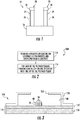
- FIG. 1 is a sectional view of an example surface enhanced luminescence (SELS) sensor 20 that may be used for sensing the interaction between light and an analyte deposited upon sensor 20.
- sensor 20 facilitates testing or diagnosis using surface enhanced Raman spectroscopy (SERS).
- SERS surface enhanced Raman spectroscopy
- sensor 20 comprises nano fingers form from polymer pillars, wherein the coating layer covers the sidewalls of the polymer pillars and wherein each of the pillars has a metal cap that is supported by and in contact with a top of each of the pillars. The coating layer reduces contamination of the metal and of the analyte being tested from the underlying material of the polymer pillars.
- the coating layer does not encapsulate a top of the polymer pillars, securement of the metal cap to the top of the polymer pillar is facilitated.
- the coating layer is further used to tune or control the rigidity of the polymer pillar.
- Sensor 20 comprises substrate 24, and nano fingers 28.
- Substrate 24 comprises a base or foundation for supporting nano fingers 28.
- substrate 24 comprises a layer of silicon, quartz, glass or polymeric films such as polyethylene terephthalate (PET).
- PET polyethylene terephthalate
- substrate 24 may additionally comprise an interlayer of a dielectric material between the silicon substrate and nano fingers 28.
- Such an interlayer dielectric may be formed from a material such as SiO 2 TEOS, a passivation layer of SiC, silicon nitride etc. In other implementations, other interlayer dielectric materials may be utilized.
- substrate 24 may be formed from other materials such as quartz, ceramics, polymers and other materials.
- Nano fingers 28 comprise elongated comprise flexible columnar supports such as needles, fingers, particles or wires.
- such nano fingers 28 are formed from materials and/or are dimensioned so as to bend or flex towards and away from one another in response to applied electric fields.
- such nano fingers 28 have an aspect ratio of and at least 10:1 (a height of at least 10 times the thickness or diameter).
- such nano fingers 28 have a thickness or diameter between 50 nm and 100 nm, while, at the same time, having a height of at least 500 nm and, in one implementation, at least 700 nm.
- the nano fingers 28 are movable and are self-actuating, wherein such columnar structures bend or flex towards one another in response to micro-capillary forces so as to self-organize, wherein such bending facilitates close spacing between the structures for greater scattered radiation intensity.
- each of nano fingers 28 comprises pillar 34, coating layer 36 and metal 40.
- Pillar 34 comprises an elongate column formed from a polymer material.
- the polymer material facilitates the use of molding, imprinting or other fabrication techniques to form pillars 34.
- the polymer material further facilitates bending and flexing of pillars 34 and subsequently closing during use of sensor 20.
- polymer materials from which each pillar 34 may be formed include, but are not limited to, photo resist, PDMS, or a flexible material selected from the group, which includes both dielectric and non-dielectric materials, consisting of a highly cross-linked uv-curable or thermal-curable polymer, a highly cross-linked uv-curable or thermal-curable plastic, a polysiloxane compound, silicon, silicon dioxide, spin-on glass, a solgel material, silicon nitride, diamond, diamond-like carbon, aluminum oxide, sapphire, zinc oxide, and titanium dioxide.
- Coating layer 36 comprises a thin layer or film of at least one passivation material that conforms to and coats the exterior side wall surfaces of pillar 34.
- coating layer 36 has a uniform thickness across a majority of a height of pillar 34.
- coating layer 34 has a substantially uniform thickness the entire height of pillar 34, wherein the thickness varies by less than 10% along the entire height.
- coating layer 36 has a thickness of at least 1 nm. In one implementation, coating layer 36 has a thickness of at least 1 nm and no greater than 20 nm.
- coating layer 36 comprises a material that is less likely to emit contaminants or contaminate metal cap 40 during the fabrication or use of sensor 20 as compared to the material or materials of pillar 34.
- coating layer 36 comprises an organic material such as polytetrafluoroethylene, parylene or other conformal coating.
- coating layer 36 comprises at least one inorganic material. Examples of materials from which coating layer 36 may be formed include, but are not limited to, SlO 2 , silicon nitride, titanium oxide, tantalum oxide, hafnium oxide, tungsten oxide, aluminum oxide, zirconium oxide etc..
- the materials chosen for coating layer 36 comprise materials that may be depositable by atomic layer deposition (ALD), physical vapor deposition (PVD), chemical vapor deposition (CVD) such as plasma enhanced chemical vapor deposition (PECVD).
- ALD atomic layer deposition
- PVD physical vapor deposition
- CVD chemical vapor deposition
- PECVD plasma enhanced chemical vapor deposition
- coating layer 36 may comprise other materials deposited or formed upon the exterior side wall surfaces of pillar 34 in other fashions.
- coating layer 36 is applied directly to and in contact with the side wall surfaces of pillar 34. In one implementation, coating layer 36 is applied and adheres directly to pillar 34. In yet another implementation, coating layer 36 may be secured to the side wall surfaces of pillar 34 by an intermediate adhesive layer.
- the material or materials chosen for coating layer 36, the chosen thickness for coating layer 36, the material or materials chosen for pillar 34 and the thickness for pillar 34 may be selected so as to tune or control the bendability or flexibility (rigidity) of each nano finger 28.
- the thickness of pillar 34 may be reduced to a point of having too great a degree of flexibility or bendability, wherein the thickness and/or materials chosen for coating layer 36 serve to increase the rigidity of the final nano finger 28 such that the flexibility falls within an acceptable range.
- the height of pillar 34 may be increased to a point of having to greater degree of flexibility or bend ability, wherein the thickness and/or materials chosen for coating layer 36 serve to increase the rigidity of the final nano finger 28 such that the flexibility falls within an acceptable range.
- Metal cap 40 comprises a metallic structure formed on top of pillar 34 in direct contact with pillar 34. Because metal cap 40 is in direct contact with the top of pillar 34, metal cap 40 may have greater adherence to pillar 34, regardless of the material chosen for coating layer 36. Metal cap 40 has a bottom surface that does not overlap or cover coating layer 36. Metal cap 40 has a top surface that is not covered by cover layer 36, so as to be exposed to the liquid to be tested. Although metal cap 40 is illustrated as being substantially rectangular, it should be appreciated that metal cap 40 may have a variety of different sizes and shapes. For example, in some implementations, metal cap 40 may be more spherical in shape.
- Metal cap 40 comprises a metal material that enhances the intensity of electromagnetic radiation emitted as a result of the reaction of the analyte and the light impinging the analyte upon nano fingers 28.
- metal cap 40 comprises silver, gold, copper, platinum, aluminum, or combinations of these metals in the form of alloys or multilayer systems.
- metal cap 40 may comprise other metallic materials that provide such intensity enhancement. According to the invention, metal cap 40 is not covered or coated by coating layer 36.
- coating layer 36 enhances the performance and shelf life of the nano fingers 28 by preventing contaminants from leaching out of the polymer of the pillars 34 and reducing the cleanliness of the metal cap 40. Direct chemisoption onto the clean metal of cap 40 provides robust coupling to enhance the plasmonic resonance of the device. Coating layer 36 may also improve the stiffness properties of nano fingers 28 such that nano fingers 28 may be more uniformly collapse. In some implementations, coating layer 36 is tuned for different solvents. For example, ethanol and water are the two example solvents that may be used during testing; however, with different finger stiffnesses and chemical protection of the polymer, the number of suitable solvents for the analyte during testing may be expanded.
- FIG. 2 is a flow diagram illustrating one example method 100 for forming a SELS sensor, such as SELS sensor 20 illustrated in Figure 1 .
- SELS sensor 20 comprises a surface enhance Raman spectroscopy (SERS) sensor.
- SERS surface enhance Raman spectroscopy
- coating layer 36 is formed on the side walls of pillar 34 which extends from substrate 24.
- the coating layer 36 is formed on the side walls of pillar 34 using plasma enhanced chemical vapor deposition.
- the coating layer formed on the side walls of pillar 34 using atomic layer deposition.
- the coating layer 36 may be formed using other techniques.
- coating layer 36 is formed directly upon the outer side wall surfaces of pillar 34.
- an intermediate adhesive layer is first applied to the outer side wall surfaces of pillar 34, wherein coating layer 36 comprises a layer over the adhesive layer and held to pillar 34 by the adhesive layer.
- metal cap 40 is formed on and in contact with the top of each polymer pillar 34.
- the forming of coating layer 36 on pillars 34 is controlled to limit an extent of coverage of coating 36 so as to not completely cover the top of pillar 34.
- portions of coating 36 extending over the top of pillar 34 are subsequently removed to expose the top of pillar 34 for direct contact with metal cap 40.
- metal cap 40 is deposited directly onto the top surface of each pillar 34 using a plasma coating deposition technique such as physical vapor deposition (PVD).
- PVD physical vapor deposition
- metal cap 40 comprises a metal such as gold or silver.
- metal cap 40 may be formed or deposited on top of pillar 34 in other fashions with the same or other materials.
- FIG. 3 is a sectional view illustrating another example SELS Sensor 120.
- Sensor 120 comprises substrate 124, housing 126 and nano fingers 28 described above.
- Substrate 124 is similar to substrate 24 described above except that substrate 124 is specifically illustrated as comprising base substrate layer 150 and substrate interlayer 152.
- Base substrate layer 150 comprises a foundation for apparatus 120, supporting interlayer 152.
- base substrate layer 150 comprises a layer of silicon.
- base substrate layer 150 may comprise other materials.
- Interlayer 152 comprises a dielectric layer extending on top of layer 150 and supporting nano fingers 28. In the example illustrated, interlayer 152 is further sandwiched between housing 126 and layer 150. In other implementations, layer 152 is contained within housing 126, wherein housing 126 is directly in contact with layer 150. In one implementation, interlayer 152 comprises a layer formed from a material such as SiO 2 TEOS. In other implementations, other interlayer dielectric materials may be utilized.
- Housing 126 comprises an enclosure or other structure extending about nano fingers 28 on substrate 124 and forming a chamber 160 for receiving and containing a liquid solution containing an analyte to be examined or tested. Housing 126 protects nano fingers 28 from exposure to the environment and reduces or prevents oxidation of surfaces of nano fingers 28 prior to use. Housing 126 may additionally reduce or prevent unintentional or premature exposure of nano fingers 28 to extraneous substances or an analyte that nano fingers 28 are intended to detect. Although housing 126 and substrate 124 are illustrated as forming a rectangular shaped interior chamber 160, in other implementations, chamber 160 may have other shapes.
- housing 126 is illustrated as having a top opening 162 through which the liquid is applied to chamber 160, in other implementations, opening 162 may alternatively extend through a side of housing 126. In some implementations, housing 126 may additionally support an integrated lens located for focusing light or laser light onto the tips of metal caps 40 of nano fingers 28.
- Nano fingers 28 are described above.
- Figures 4A and 4B illustrate portions of the example sensor 120 prior to closing of nano fingers 28.
- Figures 5A and 5B illustrate the bending or flexing of nano fingers 28, the closing of nano fingers 28 to capture analyte molecules of interest to be sensed.
- nano fingers 28 are substantially vertical, having the illustrated spacing between the individual nano fingers 28.
- liquid solution 180 containing analyte molecules 181 (schematically shown) are deposited on and about nano fingers 28. The liquid solution 180 may cover and coat nano fingers 28.
- the liquid solution 180 applied in figures 4A and 4B is evaporated, leaving the remaining analyte molecules 181.
- the evaporation may result in nano fingers 28 flexing or bending towards one another so as to capture or entrap the analyte molecules 181 therebetween.
- capillary forces resulting from the evaporation of liquid solution 180 may cause nano fingers 28 to flex or bend towards one another or close.
- the retained analyte molecules 181 and the closed nano fingers 28 with metal caps 40 intensify signals or light emitted from sensor 120 in response to interactions between the light or laser impinging nano fingers 28 and analyte molecules 181.
- FIG. 6 is a sectional view of another example SELS sensor 220.
- Sensor 220 is similar to sensor 20 except that sensor 220 comprises coating layer 236 in place of coating layer 36. Those remaining components of sensor 220 which correspond to components of sensor 20 are numbered similarly.
- Coating layer 236 is similar coating layer 36 except that coating layer 236 has a non-uniform or irregular thickness in a direction parallel to our along along the vertical height of pillars 34. In the example illustrated, coating layer 236 has a thickness that decreases from adjacent the top of pillars 34 towards substrate 24. As a result, lower portions of each nano finger 28 are less rigid as compared to the lower portions of nano fingers 28 of sensor 20. The lower rigidity at the base or lower portion of each of nano fingers 28 provided by coating layer 236 may enhance the ability of nano fingers 28 to flex or bend when closing as shown in Figures 5A and 5B .
- coating layer 236 has a uniform thickness about the vertical centerline of impeller 34, but wherein the thickness gradually and linearly decreases as coating 236 approaches substrate 24.
- a upper portions (such as above the vertical midpoint of pillars 34) of coating layer 236 have a thickness of greater than 10 nm, and in one implementation, greater than 15 nm while lower portions (such as below the vertical midpoint of pillars 34) of coating layer 236 have a thickness of less than 10 nm, and in one implementation, less than 5 nm.
- coating layer 236 extends from metal cap 40 only down to the top of substrate 24 to completely encompass all side surfaces of pillars 34 for contamination reduction.
- coating layer 236 and have other thickness profiles.
- coating layer 236 may extend along selected portions of the side surfaces of pillars 34.
- coating layer 236 may terminate prior to reaching substrate 24.
- coating layer 236 may alternatively undergo thickness variations are changes in a stepped or stepwise manner vertically along pillars 34.
- sensor 220 may additionally comprise coating layer 237 formed upon the upper surface of substrate 24, between nano fingers 28 and about nano fingers 28.
- coating layer 237 is the same material or materials as coating layer 36.
- coating layer 236 is formed upon substrate 24 independent of the formation of coating layer 26 on the side wall surfaces of pillars 34.
- coating layer 237 concurrently formed upon substrate 24 with the deposition of coating layer 236 on the side wall surfaces of pillars 34.
- coating layers 236 and 237 may be both formed at the same time by plasma enhanced chemical vapor deposition or atomic layer deposition.
- FIG. 7 is a sectional view illustrating another example SELS sensor, sensor 320.
- Sensor 320 is similar to sensor 20 described above except that sensor 320 comprises coating layer 336 in place of coating layer 36.
- Coating layer 336 is similar coating layer 36 except that coating layer 336 is specifically illustrated as continuously extending along side wall surfaces of a first pillar 34, across the upper surface of substrate 24 and a long side wall surfaces of a second consecutive pillars 34. In the example illustrated, coating layer 336 continuously extends from adjacent metal cap 40 of one nano finger 28 to adjacent a metal cap 40 of another nano finger 28.
- portion of the coating layer 336 extending parallel to or adjacent to the upper surface of substrate 24 may have a greater thickness as compared to the thickness of coating layer 336 extending along the side wall surfaces of pillars 34.
- the remaining components of sensor 320 which correspond to points of sensor 20 are numbered similarly.
- Figure 8 is a flow diagram of an example method 400 that may be utilized to form an SELS sensor, such as SELS sensor 320.
- the various stages of sensor 320 formed pursuant to method 400 are illustrated in Figures 9-11 and Figure 7 .
- method 400 is described with respect to forming sensor 320, method 400 may likewise be utilized to form other described sensors, such as sensors 120 are 220.
- method 400 may be utilized to form a sensor wherein the coating layer has a non-uniform thickness along the vertical height of the respective pillars as described above respect to sensor 220.
- polymer pillars 34 extending from the substrate 24 are coated with a coating layer 336 (shown in Figure 10 ).
- the coating 336 continuously extends across and over each of the pillars 34, across the tops 342, and along side wall surfaces 344 of each pillar 34.
- the coating layer 336 further continuously extends between such pillars 34 across the top surface 348 of substrate 24.
- the material that form pillars 34 may extend along the top surface 348 of substrate 24, wherein coating layer 336 coats the upper surface of this layer on substrate 24 remaining from the formation of pillars 34.
- the continuous integral layer, a single unitary homogenous layer or a multitude of stacked homogenous layers, is uninterrupted as it extends along the side wall surfaces 344 of multiple pillars 34, across the tops 342 of multiple pillars 34 and across and between the floors of such pillars, the top or upper surface 348 of substrate 24.
- coating layer 336 is formed through plasma enhanced chemical vapor deposition.
- coating layer 336 is formed as multiple molecular layers deposited by atomic layer deposition.
- the single layer or multiple stacked layers have a thickness of at least 1 nm. In one implementation, the single layer or multiple stacked layers have a thickness of at least 1 nm and less than or equal to 20 nm.
- portions of coating layer 336 that overlie the top 342 of each pillar 342 are removed so as to expose the top or upper surface 342 of each pillar 34 with the coating layer 336 on the side wall surfaces of pillars 34 being left in place or maintained.
- those portions of coating layer 336 that overlie the top 342 of each pillar 342 are removed by a blanket etch back process, wherein the top coat on top 342 is etched away but wherein the portion of coating layer 336 along side wall surfaces 344 are retained.
- the blanket extract process may comprise a CMOS spacer formation similar involving blanket etch back through reactive ion etch or plasma etch process by a fluorine or chlorine-containing gases (e.g., CF 4 , CCl 4 etc.).
- a fluorine or chlorine-containing gases e.g., CF 4 , CCl 4 etc.
- those portions of coating 336 over top surfaces 342 of pillars 34 may be selectively removed while leaving force of coating layer 336 along side wall surfaces 344 using other material removal techniques.
- metal cap 40 is formed on each of pillars 34 such a metal cap 40 is in direct contact with the top 342 of its associated pillar 34.
- Metal cap 40 is described above. Because metal cap 40 is formed directly on and in contact with exposed top surface 342 of its associated pillar 34, metal cap 40 may be more securely and reliably retained or joined to the respective pillar 34. Because those portions of coating layer 336 that overlie top surface 342 are removed, the variety and number of materials that may be utilized for coating layer 336 is enlarged as coating 336 does not extend between pillar 34 and each metal cap 40 and cannot interfere with or has a reduced impact with the securement of each metal cap 40 to the respective pillar 34.
- Figures 12-14 illustrate one example method for forming and providing substrate 24 and pillars 34 as provided in Figure 9 as part of method 400.
- Figures 12-14 illustrate the forming of substrate 24 and pillars 34 by an imprinting process.
- a polymer mass 434 is deposited upon or otherwise joined to substrate 24.
- the polymer mass 434 comprises an ultraviolet resist material.
- the polymer mass 434 comprises a polymer resist material such as a UV curable acrylate.
- the polymer mass may comprise a material or multiple materials selected from a group of materials consisting of a flexible material selected from the group, which includes both dielectric and non-dielectric materials, consisting of a highly cross-linked uv-curable or thermal-curable polymer, a highly cross-linked uv-curable or thermal-curable plastic, a polysiloxane compound, silicon, silicon dioxide, spin-on glass, a solgel material, silicon nitride, diamond, diamond-like carbon, aluminum oxide, sapphire, zinc oxide, and titanium dioxide.
- the polymer mass 434 is imprinted by a master 437.
- master 437 comprises a plurality of projections 439 which are spaced or which provide openings 441 corresponding in size, shape and location of the to be formed pillars 34 (described above).
- master 437 is imprinted into polymer mass 434 allowing the material of mass 434 to flow about and surround each of projections 439. While the material of mass 434 surrounds projections 439, the polymer mass 434 is allowed to solidify or harden.
- the polymer mass 434 is cured with an ultraviolet light. Thereafter, the master 437 is removed, leaving the substrate 24 and pillars 34 shown in Figure 9 , ready for the remaining steps of method 400 to be carried out.
- Figures 12-14 illustrate one example method for providing substrate 24 and pillars 34 shown in Figure 9 .
- pillars 34 may be formed upon substrate 24 in other fashions.
- pillars 34 may be formed by other etching processes, other molding processes, other material removal processes, or by material additive processes such as three-dimensional printing.
Landscapes
- Health & Medical Sciences (AREA)
- Chemical & Material Sciences (AREA)
- Engineering & Computer Science (AREA)
- General Physics & Mathematics (AREA)
- Physics & Mathematics (AREA)
- General Health & Medical Sciences (AREA)
- Life Sciences & Earth Sciences (AREA)
- Nanotechnology (AREA)
- Analytical Chemistry (AREA)
- Nuclear Medicine, Radiotherapy & Molecular Imaging (AREA)
- Biochemistry (AREA)
- Immunology (AREA)
- Pathology (AREA)
- Crystallography & Structural Chemistry (AREA)
- Molecular Biology (AREA)
- Condensed Matter Physics & Semiconductors (AREA)
- Manufacturing & Machinery (AREA)
- Investigating, Analyzing Materials By Fluorescence Or Luminescence (AREA)
Claims (14)
- Sensor (20) für oberflächenverstärkte Lumineszenz (Surface Enhanced Luminescence Sensor - SELS), der Folgendes umfasst:ein Substrat (24);Nanofinger (28), die von dem Substrat hervorstehen, wobei jeder der Nanofinger Folgendes umfasst:eine Polymersäule (34), die eine Seitenwand und eine Oberseite aufweist;eine Beschichtungslage (36), die die Seitenwand bedeckt; undeine Metallkappe (40), die durch die Oberseite der Säule (34) getragen wird und mit ihr in Berührung steht, undwobei die Beschichtungslage (36) nicht durch die Metallkappe (40) bedeckt ist und wobei die Metallkappe (40) eine freigelegte obere Oberfläche aufweist, die nicht durch die Beschichtungslage (36) bedeckt ist.
- Sensor nach Anspruch 1, wobei das Metall Gold oder Silber, Cu, In, Pt, Rh und Kombinationen davon als Legierungen oder Mehrlagensysteme umfasst.
- Sensor nach Anspruch 1, wobei die Beschichtungslage eine Dicke von wenigstens 1 nm und höchstens 20 nm aufweist.
- Sensor nach Anspruch 1, wobei die Beschichtungslage Polytetrafluorethylen umfasst.
- Sensor nach Anspruch 1, wobei die Beschichtungslage wenigstens ein Material umfasst, das aus einer Gruppe von Materialien ausgewählt ist, die aus SiO2 und SiN besteht.
- Sensor nach Anspruch 1, wobei die Beschichtungslage eine erste Dicke nahe der Oberseite und eine zweite Dicke, die geringer als die erste Dicke ist, nahe des Substrats aufweist.
- Sensor nach Anspruch 1, wobei das Polymermaterial ein Polymer umfasst, das aus einer Gruppe von Polymeren ausgewählt ist, die aus Methacrylat, Propylen, Ethylen, Vinylidendifluorid, Vinylidenchlorid, Styrol, Acrylnitril, Tetrafluorethylen und Vinylacetat besteht.
- Verfahren zum Ausbilden eines Sensors für oberflächenverstärkte Lumineszenz (SELS) (20), wobei das Verfahren Folgendes umfasst:Bereitstellen eines Substrats (24);Ausbilden von Nanofingern (28), die von dem Substrat (24) hervorstehen, wobei jeder der Nanofinger (28) eine Polymersäule (34) umfasst, die eine Seitenwand und eine Oberseite aufweist;Ausbilden einer Beschichtungslage (36), die die Seitenwand jeder der Polymersäulen (34) bedeckt; undAusbilden einer Metallkappe (40), die durch die Oberseite jeder der Polymersäulen (34) getragen wird und mit ihr derart in Berührung steht, dass die Beschichtungslage (36) nicht durch die Metallkappe (40) bedeckt ist und derart, dass die Metallkappe (40) eine freigelegte obere Oberfläche aufweist, die nicht durch die Beschichtungslage (36) bedeckt ist.
- Verfahren nach Anspruch 8, wobei das Ausbilden der Beschichtungslage Folgendes umfasst:Beschichten der Seitenwände und der Oberseite der Polymersäulen mit der Beschichtungslage; undEntfernen von Abschnitten der Beschichtungslage, die über der Oberseite jeder Polymersäule aufliegen.
- Verfahren nach Anspruch 9, wobei die Polymersäulen mit der Beschichtungslage unter Verwendung einer plasmaunterstützten chemischen Gasphasenabscheidung (Plasma Enhanced Chemical Vapor Deposition - PECVD) beschichtet werden.
- Verfahren nach Anspruch 8, das ferner das Ausbilden der Polymersäulen durch Bedrucken einer Polymermasse mit einem die Säulen definierenden Master umfasst.
- Verfahren nach Anspruch 11, wobei die Polymermasse einen Ultraviolett-Fotolack umfasst und wobei das Verfahren ferner Folgendes umfasst:Härten des Ultraviolett-Fotolacks während der Ultraviolett-Fotolack durch den Master bedruckt wird; undEntziehen des Masters.
- Verfahren nach Anspruch 11, wobei dem Schritt des Ausbildens einer Metallkappe (40) auf und in Berührung mit der Oberseite der Polymersäulen (34) ein Schritt des Entfernens von Abschnitten der Beschichtungslage (36) vorausgeht, die über der Oberseite jeder Polymersäule (34) aufliegen.
- Verfahren nach Anspruch 13, wobei die Beschichtungslage wenigstens ein Material umfasst, das aus einer Gruppe von Materialien ausgewählt ist, die aus SiO2, SiN und Polytetrafluorethylen besteht.
Applications Claiming Priority (1)
| Application Number | Priority Date | Filing Date | Title |
|---|---|---|---|
| PCT/US2016/028683 WO2017184155A1 (en) | 2016-04-21 | 2016-04-21 | Sels nano finger sidewall coating layer |
Publications (3)
| Publication Number | Publication Date |
|---|---|
| EP3374757A1 EP3374757A1 (de) | 2018-09-19 |
| EP3374757A4 EP3374757A4 (de) | 2019-07-03 |
| EP3374757B1 true EP3374757B1 (de) | 2021-09-01 |
Family
ID=60116244
Family Applications (1)
| Application Number | Title | Priority Date | Filing Date |
|---|---|---|---|
| EP16899646.0A Active EP3374757B1 (de) | 2016-04-21 | 2016-04-21 | Sels-nanofinger-seitenwand-beschichtungsschicht |
Country Status (4)
| Country | Link |
|---|---|
| US (1) | US11320379B2 (de) |
| EP (1) | EP3374757B1 (de) |
| CN (1) | CN108603837B (de) |
| WO (1) | WO2017184155A1 (de) |
Families Citing this family (2)
| Publication number | Priority date | Publication date | Assignee | Title |
|---|---|---|---|---|
| EP4216294A1 (de) * | 2022-01-25 | 2023-07-26 | Nederlandse Organisatie voor toegepast-natuurwetenschappelijk Onderzoek TNO | Verfahren zum formen einer piezoelektrischen säulenvorrichtung |
| CN117405651B (zh) * | 2023-12-15 | 2024-03-22 | 武汉理工大学 | 镀铑金属毛细管及其制备方法、气体拉曼光谱检测系统 |
Family Cites Families (15)
| Publication number | Priority date | Publication date | Assignee | Title |
|---|---|---|---|---|
| US7460224B2 (en) | 2005-12-19 | 2008-12-02 | Opto Trace Technologies, Inc. | Arrays of nano structures for surface-enhanced Raman scattering |
| US7236242B2 (en) * | 2005-01-27 | 2007-06-26 | Hewlett-Packard Development Company, L.P. | Nano-enhanced Raman spectroscopy-active nanostructures including elongated components and methods of making the same |
| US7292334B1 (en) | 2005-03-25 | 2007-11-06 | Hewlett-Packard Development Company, L.P. | Binary arrays of nanoparticles for nano-enhanced Raman scattering molecular sensors |
| US20100193768A1 (en) * | 2005-06-20 | 2010-08-05 | Illuminex Corporation | Semiconducting nanowire arrays for photovoltaic applications |
| US7832416B2 (en) * | 2006-10-10 | 2010-11-16 | Hewlett-Packard Development Company, L.P. | Imprint lithography apparatus and methods |
| US7612883B2 (en) * | 2007-05-17 | 2009-11-03 | General Electric Company | Dynamic plasmonics-enabled signal enhancement, a device comprising the same, and a method using the same |
| EP2491372B1 (de) | 2009-10-23 | 2021-07-21 | Danmarks Tekniske Universitet | Oberflächenverstärkte ramanstreuungssubstrate für raman-spektroskopie |
| CN102947681B (zh) | 2010-04-20 | 2016-05-18 | 惠普发展公司,有限责任合伙企业 | 用于表面增强发光的自动布置、发光增强器件 |
| WO2012087352A2 (en) * | 2010-12-20 | 2012-06-28 | The Regents Of The University Of California | Superhydrophobic and superoleophobic nanosurfaces |
| WO2012128762A1 (en) * | 2011-03-23 | 2012-09-27 | Hewlett-Packard Development Company, L.P. | Hybrid nanostructures for molecular analysis |
| US9001322B2 (en) | 2011-08-30 | 2015-04-07 | Cornell University | Surface enhanced raman scattering (SERS) apparatus, methods and applications |
| US8520202B2 (en) * | 2011-09-15 | 2013-08-27 | Hewlett-Packard Development Company, L.P. | Asymmetrical-nanofinger device for surface-enhanced luminescense |
| EP2948757B1 (de) | 2013-01-25 | 2017-04-26 | Hewlett-Packard Development Company, L.P. | Chemische sensorvorrichtung |
| WO2015026297A1 (en) | 2013-08-20 | 2015-02-26 | Agency For Science, Technology And Research | Spectroscopic device, method of detecting surface-enhanced raman scattering (sers) signal, and method for multiplex detection of a plurality of volatile organic compounds using surface-enhanced raman scattering (sers) |
| WO2015141885A1 (ko) | 2014-03-21 | 2015-09-24 | 금오공과대학교 산학협력단 | MB-GNR/SiO2 나노복합체, 이의 제조방법 및 이를 포함하는 암치료제 |
-
2016
- 2016-04-21 CN CN201680079718.1A patent/CN108603837B/zh active Active
- 2016-04-21 EP EP16899646.0A patent/EP3374757B1/de active Active
- 2016-04-21 US US16/074,331 patent/US11320379B2/en active Active
- 2016-04-21 WO PCT/US2016/028683 patent/WO2017184155A1/en active Application Filing
Also Published As
| Publication number | Publication date |
|---|---|
| EP3374757A4 (de) | 2019-07-03 |
| WO2017184155A1 (en) | 2017-10-26 |
| CN108603837B (zh) | 2021-07-06 |
| US20210190687A1 (en) | 2021-06-24 |
| CN108603837A (zh) | 2018-09-28 |
| US11320379B2 (en) | 2022-05-03 |
| EP3374757A1 (de) | 2018-09-19 |
Similar Documents
| Publication | Publication Date | Title |
|---|---|---|
| US10354866B2 (en) | Equipment and method to automatically transfer a graphene monolayer to a substrate | |
| US8518829B2 (en) | Self-sealed fluidic channels for nanopore array | |
| US9638625B2 (en) | Apparatus for filtering species | |
| US20140218727A1 (en) | Apparatus for use in a sensing application having a destructible cover | |
| Gupta et al. | Hydrogen plasma treatment of silicon dioxide for improved silane deposition | |
| JP6691234B2 (ja) | 基板アセンブリ及び関連方法 | |
| IL152271A (en) | Structures of micro needles and manufacturing methods | |
| JP2017520878A (ja) | Cmosに基づくマイクロホットプレート上の半導体デバイス及び製作方法 | |
| EP3374757B1 (de) | Sels-nanofinger-seitenwand-beschichtungsschicht | |
| CN104515737A (zh) | 在微流体结构中产生化学物图案的方法 | |
| TW201339090A (zh) | 微機電系統奈米結構之製造方法 | |
| JP6277188B2 (ja) | マイクロキャリアの製造方法 | |
| EP2485039A1 (de) | Mikrokanal-Chip und Mikroanalysesystem | |
| US10890486B2 (en) | Plasmonic nanostructure including sacrificial passivation coating | |
| KR20200004442A (ko) | 유체 어셈블리 기판 및 그 제조방법 | |
| EP3446105B1 (de) | Nanofingererwärmung durch oberflächenverstärkte raman-streuung | |
| US10871449B2 (en) | SERS sensor apparatus with passivation film | |
| US10458918B2 (en) | Substance detection device | |
| US11255792B2 (en) | SERS sensor | |
| US11199499B2 (en) | Surface enhanced luminescence analyte interrogation stage with sacrificial coating | |
| US11460401B2 (en) | Method of fabricating an array of plasmonic structures, a biosensor and a method of fabricating a biosensor | |
| US20210181104A1 (en) | Surface enhanced liminescence analyte interrogation stage shipping and storage package | |
| EP3625526B1 (de) | Spektroskop mit designgruppen | |
| US20210199581A1 (en) | Photocatalytic layer on plasmonically active surface | |
| Kumar | Micromachining of Single Cell Array for Oxygen Consumption Rate Analysis |
Legal Events
| Date | Code | Title | Description |
|---|---|---|---|
| STAA | Information on the status of an ep patent application or granted ep patent |
Free format text: STATUS: THE INTERNATIONAL PUBLICATION HAS BEEN MADE |
|
| PUAI | Public reference made under article 153(3) epc to a published international application that has entered the european phase |
Free format text: ORIGINAL CODE: 0009012 |
|
| STAA | Information on the status of an ep patent application or granted ep patent |
Free format text: STATUS: REQUEST FOR EXAMINATION WAS MADE |
|
| 17P | Request for examination filed |
Effective date: 20180615 |
|
| AK | Designated contracting states |
Kind code of ref document: A1 Designated state(s): AL AT BE BG CH CY CZ DE DK EE ES FI FR GB GR HR HU IE IS IT LI LT LU LV MC MK MT NL NO PL PT RO RS SE SI SK SM TR |
|
| AX | Request for extension of the european patent |
Extension state: BA ME |
|
| RAP1 | Party data changed (applicant data changed or rights of an application transferred) |
Owner name: HEWLETT-PACKARD DEVELOPMENT COMPANY, L.P. |
|
| A4 | Supplementary search report drawn up and despatched |
Effective date: 20190531 |
|
| RIC1 | Information provided on ipc code assigned before grant |
Ipc: G01N 21/64 20060101AFI20190524BHEP Ipc: G01N 21/65 20060101ALI20190524BHEP Ipc: G01N 33/553 20060101ALI20190524BHEP |
|
| DAV | Request for validation of the european patent (deleted) | ||
| DAX | Request for extension of the european patent (deleted) | ||
| GRAP | Despatch of communication of intention to grant a patent |
Free format text: ORIGINAL CODE: EPIDOSNIGR1 |
|
| STAA | Information on the status of an ep patent application or granted ep patent |
Free format text: STATUS: GRANT OF PATENT IS INTENDED |
|
| INTG | Intention to grant announced |
Effective date: 20210624 |
|
| GRAS | Grant fee paid |
Free format text: ORIGINAL CODE: EPIDOSNIGR3 |
|
| GRAA | (expected) grant |
Free format text: ORIGINAL CODE: 0009210 |
|
| STAA | Information on the status of an ep patent application or granted ep patent |
Free format text: STATUS: THE PATENT HAS BEEN GRANTED |
|
| AK | Designated contracting states |
Kind code of ref document: B1 Designated state(s): AL AT BE BG CH CY CZ DE DK EE ES FI FR GB GR HR HU IE IS IT LI LT LU LV MC MK MT NL NO PL PT RO RS SE SI SK SM TR |
|
| REG | Reference to a national code |
Ref country code: GB Ref legal event code: FG4D |
|
| REG | Reference to a national code |
Ref country code: CH Ref legal event code: EP Ref country code: AT Ref legal event code: REF Ref document number: 1426725 Country of ref document: AT Kind code of ref document: T Effective date: 20210915 |
|
| REG | Reference to a national code |
Ref country code: DE Ref legal event code: R096 Ref document number: 602016063298 Country of ref document: DE |
|
| REG | Reference to a national code |
Ref country code: IE Ref legal event code: FG4D |
|
| REG | Reference to a national code |
Ref country code: LT Ref legal event code: MG9D |
|
| REG | Reference to a national code |
Ref country code: NL Ref legal event code: MP Effective date: 20210901 |
|
| PG25 | Lapsed in a contracting state [announced via postgrant information from national office to epo] |
Ref country code: FI Free format text: LAPSE BECAUSE OF FAILURE TO SUBMIT A TRANSLATION OF THE DESCRIPTION OR TO PAY THE FEE WITHIN THE PRESCRIBED TIME-LIMIT Effective date: 20210901 Ref country code: ES Free format text: LAPSE BECAUSE OF FAILURE TO SUBMIT A TRANSLATION OF THE DESCRIPTION OR TO PAY THE FEE WITHIN THE PRESCRIBED TIME-LIMIT Effective date: 20210901 Ref country code: HR Free format text: LAPSE BECAUSE OF FAILURE TO SUBMIT A TRANSLATION OF THE DESCRIPTION OR TO PAY THE FEE WITHIN THE PRESCRIBED TIME-LIMIT Effective date: 20210901 Ref country code: NO Free format text: LAPSE BECAUSE OF FAILURE TO SUBMIT A TRANSLATION OF THE DESCRIPTION OR TO PAY THE FEE WITHIN THE PRESCRIBED TIME-LIMIT Effective date: 20211201 Ref country code: BG Free format text: LAPSE BECAUSE OF FAILURE TO SUBMIT A TRANSLATION OF THE DESCRIPTION OR TO PAY THE FEE WITHIN THE PRESCRIBED TIME-LIMIT Effective date: 20211201 Ref country code: LT Free format text: LAPSE BECAUSE OF FAILURE TO SUBMIT A TRANSLATION OF THE DESCRIPTION OR TO PAY THE FEE WITHIN THE PRESCRIBED TIME-LIMIT Effective date: 20210901 Ref country code: RS Free format text: LAPSE BECAUSE OF FAILURE TO SUBMIT A TRANSLATION OF THE DESCRIPTION OR TO PAY THE FEE WITHIN THE PRESCRIBED TIME-LIMIT Effective date: 20210901 Ref country code: SE Free format text: LAPSE BECAUSE OF FAILURE TO SUBMIT A TRANSLATION OF THE DESCRIPTION OR TO PAY THE FEE WITHIN THE PRESCRIBED TIME-LIMIT Effective date: 20210901 |
|
| REG | Reference to a national code |
Ref country code: AT Ref legal event code: MK05 Ref document number: 1426725 Country of ref document: AT Kind code of ref document: T Effective date: 20210901 |
|
| PG25 | Lapsed in a contracting state [announced via postgrant information from national office to epo] |
Ref country code: PL Free format text: LAPSE BECAUSE OF FAILURE TO SUBMIT A TRANSLATION OF THE DESCRIPTION OR TO PAY THE FEE WITHIN THE PRESCRIBED TIME-LIMIT Effective date: 20210901 Ref country code: LV Free format text: LAPSE BECAUSE OF FAILURE TO SUBMIT A TRANSLATION OF THE DESCRIPTION OR TO PAY THE FEE WITHIN THE PRESCRIBED TIME-LIMIT Effective date: 20210901 Ref country code: GR Free format text: LAPSE BECAUSE OF FAILURE TO SUBMIT A TRANSLATION OF THE DESCRIPTION OR TO PAY THE FEE WITHIN THE PRESCRIBED TIME-LIMIT Effective date: 20211202 |
|
| PG25 | Lapsed in a contracting state [announced via postgrant information from national office to epo] |
Ref country code: AT Free format text: LAPSE BECAUSE OF FAILURE TO SUBMIT A TRANSLATION OF THE DESCRIPTION OR TO PAY THE FEE WITHIN THE PRESCRIBED TIME-LIMIT Effective date: 20210901 |
|
| PG25 | Lapsed in a contracting state [announced via postgrant information from national office to epo] |
Ref country code: IS Free format text: LAPSE BECAUSE OF FAILURE TO SUBMIT A TRANSLATION OF THE DESCRIPTION OR TO PAY THE FEE WITHIN THE PRESCRIBED TIME-LIMIT Effective date: 20220101 Ref country code: SM Free format text: LAPSE BECAUSE OF FAILURE TO SUBMIT A TRANSLATION OF THE DESCRIPTION OR TO PAY THE FEE WITHIN THE PRESCRIBED TIME-LIMIT Effective date: 20210901 Ref country code: SK Free format text: LAPSE BECAUSE OF FAILURE TO SUBMIT A TRANSLATION OF THE DESCRIPTION OR TO PAY THE FEE WITHIN THE PRESCRIBED TIME-LIMIT Effective date: 20210901 Ref country code: RO Free format text: LAPSE BECAUSE OF FAILURE TO SUBMIT A TRANSLATION OF THE DESCRIPTION OR TO PAY THE FEE WITHIN THE PRESCRIBED TIME-LIMIT Effective date: 20210901 Ref country code: PT Free format text: LAPSE BECAUSE OF FAILURE TO SUBMIT A TRANSLATION OF THE DESCRIPTION OR TO PAY THE FEE WITHIN THE PRESCRIBED TIME-LIMIT Effective date: 20220103 Ref country code: NL Free format text: LAPSE BECAUSE OF FAILURE TO SUBMIT A TRANSLATION OF THE DESCRIPTION OR TO PAY THE FEE WITHIN THE PRESCRIBED TIME-LIMIT Effective date: 20210901 Ref country code: EE Free format text: LAPSE BECAUSE OF FAILURE TO SUBMIT A TRANSLATION OF THE DESCRIPTION OR TO PAY THE FEE WITHIN THE PRESCRIBED TIME-LIMIT Effective date: 20210901 Ref country code: CZ Free format text: LAPSE BECAUSE OF FAILURE TO SUBMIT A TRANSLATION OF THE DESCRIPTION OR TO PAY THE FEE WITHIN THE PRESCRIBED TIME-LIMIT Effective date: 20210901 Ref country code: AL Free format text: LAPSE BECAUSE OF FAILURE TO SUBMIT A TRANSLATION OF THE DESCRIPTION OR TO PAY THE FEE WITHIN THE PRESCRIBED TIME-LIMIT Effective date: 20210901 |
|
| REG | Reference to a national code |
Ref country code: DE Ref legal event code: R097 Ref document number: 602016063298 Country of ref document: DE |
|
| PLBE | No opposition filed within time limit |
Free format text: ORIGINAL CODE: 0009261 |
|
| STAA | Information on the status of an ep patent application or granted ep patent |
Free format text: STATUS: NO OPPOSITION FILED WITHIN TIME LIMIT |
|
| PG25 | Lapsed in a contracting state [announced via postgrant information from national office to epo] |
Ref country code: IT Free format text: LAPSE BECAUSE OF FAILURE TO SUBMIT A TRANSLATION OF THE DESCRIPTION OR TO PAY THE FEE WITHIN THE PRESCRIBED TIME-LIMIT Effective date: 20210901 Ref country code: DK Free format text: LAPSE BECAUSE OF FAILURE TO SUBMIT A TRANSLATION OF THE DESCRIPTION OR TO PAY THE FEE WITHIN THE PRESCRIBED TIME-LIMIT Effective date: 20210901 |
|
| 26N | No opposition filed |
Effective date: 20220602 |
|
| PG25 | Lapsed in a contracting state [announced via postgrant information from national office to epo] |
Ref country code: SI Free format text: LAPSE BECAUSE OF FAILURE TO SUBMIT A TRANSLATION OF THE DESCRIPTION OR TO PAY THE FEE WITHIN THE PRESCRIBED TIME-LIMIT Effective date: 20210901 |
|
| REG | Reference to a national code |
Ref country code: CH Ref legal event code: PL |
|
| REG | Reference to a national code |
Ref country code: BE Ref legal event code: MM Effective date: 20220430 |
|
| PG25 | Lapsed in a contracting state [announced via postgrant information from national office to epo] |
Ref country code: MC Free format text: LAPSE BECAUSE OF FAILURE TO SUBMIT A TRANSLATION OF THE DESCRIPTION OR TO PAY THE FEE WITHIN THE PRESCRIBED TIME-LIMIT Effective date: 20210901 Ref country code: LU Free format text: LAPSE BECAUSE OF NON-PAYMENT OF DUE FEES Effective date: 20220421 Ref country code: LI Free format text: LAPSE BECAUSE OF NON-PAYMENT OF DUE FEES Effective date: 20220430 Ref country code: CH Free format text: LAPSE BECAUSE OF NON-PAYMENT OF DUE FEES Effective date: 20220430 |
|
| PG25 | Lapsed in a contracting state [announced via postgrant information from national office to epo] |
Ref country code: BE Free format text: LAPSE BECAUSE OF NON-PAYMENT OF DUE FEES Effective date: 20220430 |
|
| PG25 | Lapsed in a contracting state [announced via postgrant information from national office to epo] |
Ref country code: IE Free format text: LAPSE BECAUSE OF NON-PAYMENT OF DUE FEES Effective date: 20220421 |
|
| PGFP | Annual fee paid to national office [announced via postgrant information from national office to epo] |
Ref country code: FR Payment date: 20230321 Year of fee payment: 8 |
|
| PGFP | Annual fee paid to national office [announced via postgrant information from national office to epo] |
Ref country code: GB Payment date: 20230321 Year of fee payment: 8 |
|
| PGFP | Annual fee paid to national office [announced via postgrant information from national office to epo] |
Ref country code: DE Payment date: 20230321 Year of fee payment: 8 |
|
| PG25 | Lapsed in a contracting state [announced via postgrant information from national office to epo] |
Ref country code: HU Free format text: LAPSE BECAUSE OF FAILURE TO SUBMIT A TRANSLATION OF THE DESCRIPTION OR TO PAY THE FEE WITHIN THE PRESCRIBED TIME-LIMIT; INVALID AB INITIO Effective date: 20160421 |
|
| PG25 | Lapsed in a contracting state [announced via postgrant information from national office to epo] |
Ref country code: MK Free format text: LAPSE BECAUSE OF FAILURE TO SUBMIT A TRANSLATION OF THE DESCRIPTION OR TO PAY THE FEE WITHIN THE PRESCRIBED TIME-LIMIT Effective date: 20210901 Ref country code: CY Free format text: LAPSE BECAUSE OF FAILURE TO SUBMIT A TRANSLATION OF THE DESCRIPTION OR TO PAY THE FEE WITHIN THE PRESCRIBED TIME-LIMIT Effective date: 20210901 |
|
| PGFP | Annual fee paid to national office [announced via postgrant information from national office to epo] |
Ref country code: GB Payment date: 20240321 Year of fee payment: 9 |