EP3373710A1 - Optoelektronikmodul - Google Patents
Optoelektronikmodul Download PDFInfo
- Publication number
- EP3373710A1 EP3373710A1 EP18151177.5A EP18151177A EP3373710A1 EP 3373710 A1 EP3373710 A1 EP 3373710A1 EP 18151177 A EP18151177 A EP 18151177A EP 3373710 A1 EP3373710 A1 EP 3373710A1
- Authority
- EP
- European Patent Office
- Prior art keywords
- film
- printed circuit
- optoelectronic module
- housing
- circuit board
- Prior art date
- Legal status (The legal status is an assumption and is not a legal conclusion. Google has not performed a legal analysis and makes no representation as to the accuracy of the status listed.)
- Granted
Links
Images





Classifications
-
- H—ELECTRICITY
- H05—ELECTRIC TECHNIQUES NOT OTHERWISE PROVIDED FOR
- H05K—PRINTED CIRCUITS; CASINGS OR CONSTRUCTIONAL DETAILS OF ELECTRIC APPARATUS; MANUFACTURE OF ASSEMBLAGES OF ELECTRICAL COMPONENTS
- H05K1/00—Printed circuits
- H05K1/02—Details
- H05K1/0274—Optical details, e.g. printed circuits comprising integral optical means
-
- G—PHYSICS
- G01—MEASURING; TESTING
- G01S—RADIO DIRECTION-FINDING; RADIO NAVIGATION; DETERMINING DISTANCE OR VELOCITY BY USE OF RADIO WAVES; LOCATING OR PRESENCE-DETECTING BY USE OF THE REFLECTION OR RERADIATION OF RADIO WAVES; ANALOGOUS ARRANGEMENTS USING OTHER WAVES
- G01S7/00—Details of systems according to groups G01S13/00, G01S15/00, G01S17/00
- G01S7/48—Details of systems according to groups G01S13/00, G01S15/00, G01S17/00 of systems according to group G01S17/00
- G01S7/481—Constructional features, e.g. arrangements of optical elements
- G01S7/4811—Constructional features, e.g. arrangements of optical elements common to transmitter and receiver
- G01S7/4813—Housing arrangements
-
- H—ELECTRICITY
- H05—ELECTRIC TECHNIQUES NOT OTHERWISE PROVIDED FOR
- H05K—PRINTED CIRCUITS; CASINGS OR CONSTRUCTIONAL DETAILS OF ELECTRIC APPARATUS; MANUFACTURE OF ASSEMBLAGES OF ELECTRICAL COMPONENTS
- H05K3/00—Apparatus or processes for manufacturing printed circuits
- H05K3/0097—Processing two or more printed circuits simultaneously, e.g. made from a common substrate, or temporarily stacked circuit boards
-
- H—ELECTRICITY
- H05—ELECTRIC TECHNIQUES NOT OTHERWISE PROVIDED FOR
- H05K—PRINTED CIRCUITS; CASINGS OR CONSTRUCTIONAL DETAILS OF ELECTRIC APPARATUS; MANUFACTURE OF ASSEMBLAGES OF ELECTRICAL COMPONENTS
- H05K3/00—Apparatus or processes for manufacturing printed circuits
- H05K3/22—Secondary treatment of printed circuits
- H05K3/28—Applying non-metallic protective coatings
- H05K3/284—Applying non-metallic protective coatings for encapsulating mounted components
-
- H—ELECTRICITY
- H05—ELECTRIC TECHNIQUES NOT OTHERWISE PROVIDED FOR
- H05K—PRINTED CIRCUITS; CASINGS OR CONSTRUCTIONAL DETAILS OF ELECTRIC APPARATUS; MANUFACTURE OF ASSEMBLAGES OF ELECTRICAL COMPONENTS
- H05K5/00—Casings, cabinets or drawers for electric apparatus
- H05K5/06—Hermetically-sealed casings
- H05K5/066—Hermetically-sealed casings sealed by fusion of the joining parts without bringing material; sealed by brazing
-
- H—ELECTRICITY
- H05—ELECTRIC TECHNIQUES NOT OTHERWISE PROVIDED FOR
- H05K—PRINTED CIRCUITS; CASINGS OR CONSTRUCTIONAL DETAILS OF ELECTRIC APPARATUS; MANUFACTURE OF ASSEMBLAGES OF ELECTRICAL COMPONENTS
- H05K2201/00—Indexing scheme relating to printed circuits covered by H05K1/00
- H05K2201/01—Dielectrics
- H05K2201/0104—Properties and characteristics in general
- H05K2201/0108—Transparent
-
- H—ELECTRICITY
- H05—ELECTRIC TECHNIQUES NOT OTHERWISE PROVIDED FOR
- H05K—PRINTED CIRCUITS; CASINGS OR CONSTRUCTIONAL DETAILS OF ELECTRIC APPARATUS; MANUFACTURE OF ASSEMBLAGES OF ELECTRICAL COMPONENTS
- H05K2201/00—Indexing scheme relating to printed circuits covered by H05K1/00
- H05K2201/01—Dielectrics
- H05K2201/0104—Properties and characteristics in general
- H05K2201/0125—Shrinkable, e.g. heat-shrinkable polymer
-
- H—ELECTRICITY
- H05—ELECTRIC TECHNIQUES NOT OTHERWISE PROVIDED FOR
- H05K—PRINTED CIRCUITS; CASINGS OR CONSTRUCTIONAL DETAILS OF ELECTRIC APPARATUS; MANUFACTURE OF ASSEMBLAGES OF ELECTRICAL COMPONENTS
- H05K2201/00—Indexing scheme relating to printed circuits covered by H05K1/00
- H05K2201/10—Details of components or other objects attached to or integrated in a printed circuit board
- H05K2201/10007—Types of components
- H05K2201/10053—Switch
-
- H—ELECTRICITY
- H05—ELECTRIC TECHNIQUES NOT OTHERWISE PROVIDED FOR
- H05K—PRINTED CIRCUITS; CASINGS OR CONSTRUCTIONAL DETAILS OF ELECTRIC APPARATUS; MANUFACTURE OF ASSEMBLAGES OF ELECTRICAL COMPONENTS
- H05K2201/00—Indexing scheme relating to printed circuits covered by H05K1/00
- H05K2201/10—Details of components or other objects attached to or integrated in a printed circuit board
- H05K2201/10007—Types of components
- H05K2201/10106—Light emitting diode [LED]
-
- H—ELECTRICITY
- H05—ELECTRIC TECHNIQUES NOT OTHERWISE PROVIDED FOR
- H05K—PRINTED CIRCUITS; CASINGS OR CONSTRUCTIONAL DETAILS OF ELECTRIC APPARATUS; MANUFACTURE OF ASSEMBLAGES OF ELECTRICAL COMPONENTS
- H05K2201/00—Indexing scheme relating to printed circuits covered by H05K1/00
- H05K2201/10—Details of components or other objects attached to or integrated in a printed circuit board
- H05K2201/10007—Types of components
- H05K2201/10121—Optical component, e.g. opto-electronic component
-
- H—ELECTRICITY
- H05—ELECTRIC TECHNIQUES NOT OTHERWISE PROVIDED FOR
- H05K—PRINTED CIRCUITS; CASINGS OR CONSTRUCTIONAL DETAILS OF ELECTRIC APPARATUS; MANUFACTURE OF ASSEMBLAGES OF ELECTRICAL COMPONENTS
- H05K2201/00—Indexing scheme relating to printed circuits covered by H05K1/00
- H05K2201/10—Details of components or other objects attached to or integrated in a printed circuit board
- H05K2201/10007—Types of components
- H05K2201/10151—Sensor
-
- H—ELECTRICITY
- H05—ELECTRIC TECHNIQUES NOT OTHERWISE PROVIDED FOR
- H05K—PRINTED CIRCUITS; CASINGS OR CONSTRUCTIONAL DETAILS OF ELECTRIC APPARATUS; MANUFACTURE OF ASSEMBLAGES OF ELECTRICAL COMPONENTS
- H05K2201/00—Indexing scheme relating to printed circuits covered by H05K1/00
- H05K2201/10—Details of components or other objects attached to or integrated in a printed circuit board
- H05K2201/10227—Other objects, e.g. metallic pieces
- H05K2201/10356—Cables
-
- H—ELECTRICITY
- H05—ELECTRIC TECHNIQUES NOT OTHERWISE PROVIDED FOR
- H05K—PRINTED CIRCUITS; CASINGS OR CONSTRUCTIONAL DETAILS OF ELECTRIC APPARATUS; MANUFACTURE OF ASSEMBLAGES OF ELECTRICAL COMPONENTS
- H05K2203/00—Indexing scheme relating to apparatus or processes for manufacturing printed circuits covered by H05K3/00
- H05K2203/13—Moulding and encapsulation; Deposition techniques; Protective layers
- H05K2203/1305—Moulding and encapsulation
- H05K2203/1311—Foil encapsulation, e.g. of mounted components
Definitions
- the invention relates to an optoelectronic module, which has a housing which completely comprises a populated printed circuit board, wherein transmitting elements and receiving elements, transmitting and receiving lenses and / or electronic components for signal processing and / or contacting for an electrical line are arranged on the printed circuit board, and methods for producing an optoelectronic module according to the preambles of claims 14 and 15, respectively.
- the invention has for its object to provide an electronic module, which has a flat housing that contributes only minimally to the total thickness of the electronic module, but still protects the Optoelectronic module reliably against environmental influences such as water vapor, chemicals or EMC.
- an optoelectronic module which has a housing which completely encloses a populated printed circuit board, transmitter elements and receiving elements, transmitting and receiving lenses and electronic components for signal processing and a contacting for an electrical line being arranged on the printed circuit board, characterized in that at least a part of the housing is formed by a tear-resistant, stable film, which connects closely to the assembled printed circuit board.
- the object is achieved in that at least a part of the housing is formed by a tear-resistant, stable film, which connects closely to the assembled printed circuit board.
- a tear-resistant, stable film which connects closely to the assembled printed circuit board.
- Such films can be designed as thin as desired, which is why they only make a small contribution to the overall thickness of the optoelectronic module. But since they reliably seal the internal electronics of the optoelectronic module, comprehensive protection against environmental influences such as water vapor, chemical, EMC influences and the like is given.
- the use of foils for the flat housing allows the production of so-called miniature flat sensors.
- the optoelectronic module forms a sensor or can be called a sensor synonymously.
- the sensor is an optoelectronic sensor.
- the sensor is a light barrier, a light sensor, a distance sensor or a similar sensor.
- the sensor has a switching output for outputting a switching signal.
- the switching output is connected via the electrical line, for example, with a controller.
- the foil forms an optical window of the sensor.
- the film is also part of the optical transmit and receive path.
- the film consists of plastic, Teflon (polytetrafluoroethylene) or metal, preferably noble metal.
- Teflon polytetrafluoroethylene
- metal preferably noble metal.
- the entire housing is formed from two foils, which are adapted by means of thermoforming the geometry or topology of the assembled printed circuit board.
- the two films are sealed together via an adhesive or welded joint.
- the entire housing is formed by a folded film, wherein the assembled circuit board is surrounded by the folded film, which is adapted by means of thermoforming the geometry or topology of the assembled printed circuit board.
- the edges of the folded films after inclusion of the assembled printed circuit board are tightly connected via adhesive or welded joints.
- the housing is formed from a front cover made of injected plastic, which is sealed cohesively with a film applied on the back of the front cover.
- a front cover can be used simultaneously for receiving optical elements, such as lenses, wherein the circuit board merely has an electronic core.
- the housing consists of two foils, between which a spacer frame is arranged, on which the two foils are attached covering the spacer frame.
- the advantage of the spacer frame lies in the flat front and rear surface of the sensor.
- the housing comprises a stiffening element.
- the housing consists of a metal foil, wherein an insulating insert element is arranged between the metal foil and the assembled printed circuit board.
- metal foils are particularly appropriate whenever the mechanical robustness of the optoelectronic module, e.g. in terms of torsional stiffness, to be increased.
- the housing consists of a rear-side, opposite the printed circuit board insulated metal foil, with which a front of a plastic cover is connected.
- the optoelectronic module mixed housing consisting of both films and plastic, can be used.
- the rear metal foil is folded up to receive the plastic cover. This has the advantage that the robustness of the optoelectronic module is increased.
- the housing which consists of at least one plastic film, has a casing of a metal foil.
- the electrical line is seamlessly surrounded by the housing.
- sealing points are eliminated, so that simultaneously with the housing, the electrical line is reliably sealed against environmental influences.
- the housing is formed by a film tube, advantageously a shrink tube.
- a heat shrink tubing the production of individual modules is very simple, since the assembled carrier plate only has to be inserted into the tube, which shrinks by heat input and encloses the assembled printed circuit board.
- a development of the invention relates to a method for producing an optoelectronic module, in which optoelectronic components and electronic components for signal processing and / or a contact can be arranged electrically connected to a support element.
- a method which is suitable for mass production a plurality of carrier elements formed as printed circuit boards are applied distributed on a film distributed to each other and the carrier elements covered by the same or a second film, wherein all film edges of the folded film or the first and the second film simultaneously cohesively be interconnected and the Optoelectronic modules are then separated.
- a further development of the invention relates to a method for producing an optoelectronic module, in which a plurality of printed circuit boards spaced from each other are arranged on a rear foil, then an assembly of the printed circuit boards with optoelectronic components takes place, which follows a lens assembly and then each assembled printed circuit board is provided with a connecting line, wherein the printed circuit boards provided with the connecting line are covered with a cover film, which is connected in a material-locking manner after being placed on a rear foil and the optoelectronic modules are separated from this composite.
- Such an approach also enables mass production to produce a high volume of these miniaturized optoelectronic modules.
- a first embodiment of an optoelectronic module according to the invention which comprises a printed circuit board 1, on which a transmitting element and a receiving element are arranged, in front of which lenses 4 are arranged. Furthermore, components for signal processing, display elements 3, as well as connection contacts 6 for connecting an electrical line 7 are located on the printed circuit board 1.
- This populated printed circuit board 1 is covered on both sides by a rear foil 8 and a front foil 9 ( Fig. 1a ), wherein the films 8 and 9 project beyond the printed circuit board 1 and the edges 10 of the films 8, 9 are joined together tightly via adhesive or welded joints.
- the films 8, 9 are optionally adapted via a thermo converter to the geometry or topology of the assembled printed circuit board, as in Fig. 1c is shown.
- Fig. 2 is used instead of two sheets only a folded sheet 11, wherein on one side of the folded sheet 11, the assembled circuit board 1 is placed, while the second half of the folded sheet 11 is folded over the assembled circuit board 1.
- the film ends of the folded film 11 are adapted to the structure of the optoelectronic module.
- the edges of the folded film 11 and the two films 8, 9 are connected to each other by means of adhesive and welded joints.
- the small thickness of the films 8, 9, 11 allows a minimal housing structure, wherein the optical components, such as lenses, directly through the films 9, 11 can be held down.
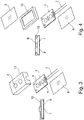
- Fig. 3 a further embodiment of the optoelectronic module according to the invention is shown, in which the assembled printed circuit board 1 is placed on a rear plastic film 8.
- the cover on the side facing the electronic components is made by a sprayed, existing plastic front cover 12, which may optionally Optogeometrien, such as lenses 4 may include.
- the printed circuit board 1 is placed on the rear plastic film 8.
- the circuit board 1 is surrounded by a spacer frame 13, which also rests on the rear sheet 8, wherein the spacer frame 13 is covered by the front sheet 9.
- the spacer frame 13 is covered by a film 8, 9 from both sides ( Fig. 4 ).
- a stiffening by suitable materials such as a steel sheet
- suitable materials such as a steel sheet
- Fig. 5 shows a further embodiment with an inner reinforcement, wherein a thin steel sheet 14 is placed under the assembled printed circuit board 1 before the welding of the films 8, 9.
- the insulation of the steel sheet 14 remains to the circuit board 1 and EMC influences are prevented.
- an external reinforcement is possible, wherein the reinforcing element in the form of the steel sheet 15 is externally attached to one of the foils 8, 9, preferably the rear foil 8.
- the steel sheet 15 can be glued to the outer rear sheet 8 or locked in a form-fitting manner (US Pat. Fig. 6 ).
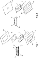
- Fig. 7 is an independent housing of two stainless steel foils 16, 17 is formed. After inserting the circuit board 1, the stainless steel sheets 16, 17 sealed circumferentially by gluing or welding.
- the front sheet 16 may have a front screen 18 which is integrated by adhesive in the front sheet 16.
- the front sheet 16 is formed as a windshield film.
- the circuit board 1 is separated by gluing or an insulating insert 19 in the form of a thin plastic plate against the backside film 17.
- FIG. 8 another embodiment of the use of stainless steel and plastic films is shown in a mixed composite.
- the backsheet 17 is formed by a metal foil, while the front foil 9 is a plastic film.
- the sealing compound is made by bonding the metal and the plastic film 17, 9.
- the assembled printed circuit board 1 is completely separated from the rear metal foil 17 by an insulating plate 20 made of plastic or an adhesive.
- a fragile, serving as a cover plastic film 9 is replaced by a molded plastic front element 21, which in particular contributes to the fact that under mechanical loads, the optoelectronic module is not damaged.
- This injection-molded front element 21 is also sealingly connected to the rear-side foil 17 consisting of metal.
- the front element can also already contain the lenses 4, in order to meet the requirements for a flat construction as possible.
- a raised edge 22 made of the metal foil 17 is carried out on the rear metal foil 17. Subsequently, the assembled printed circuit board 1 is inserted into this shell, wherein the line 7 is performed through an opening 23 of the upstand 22 to the environment. The injection-molded plastic front element 21 is then inserted into the folded-up rear metal foil 17 ( Fig. 10 ).
- Fig. 11 is shown a further embodiment of the optoelectronic module according to the invention, in which the after Fig. 2 equipped with two plastic films 8 or 9 surrounded assembled printed circuit board 1 with two metal foils 24, 25 is sheathed. There are no sealing requirements for the film composite formed by the two metal foils 24, 25. It is only a mechanical fixation to the plastic housing, such as by gluing or positive locking, necessary.
- Fig. 12 is shown as an optional alternative to the foil coating a sheath by a so-called shrink tubing possible.
- the assembled printed circuit board 1 together with line 7 is inserted into the film tube 26.
- the stretched film tube 26 contracts and surrounds the assembled printed circuit board 1.
- the cover of assembled printed circuit board 1 and line 7 takes place through this sheath transitionless.
- the optoelectronic module is welded or glued on one side by thermal influences after the wrapping of the printed circuit board 1.
- the optoelectronic module is, as already stated, connected by means of an electrical line 7 with the environment.
- Round cables, ribbon cables or printed or laminated conductor structures which are applied directly to the film 8 or 9, can be used as connection technology.
- a seal between the film housing and line 7 is required.
- the sealing of the interface 27, cable jacket to the film by a direct tight welding of the line vein material with the film (in plastic) or by an adhesive in metal foils ( Fig. 13 ).
- An elliptical connection of the interface 27 is in Fig. 14 shown.
- the welding or gluing can be done directly on the appropriate line materials or by a suitable intermediate body, which provides an optimal connection to the line and / or the film.
- An unimaged intermediate part could, for example, be supplemented as a ring-shaped element, for example, inside around for cable and outside elliptically for film.
- the electrical line 7 can also as in Fig. 15 shown, covered with the assembled printed circuit board 1 through the back sheet 8 and the front sheet 9, so that the housing formed by the backsheets 8 and the front sheet 9 seamlessly passes on the line 7, which can be dispensed with an additional seal.
- an operating element 28, for example in the form of a button, as an intermediate element in the electrical line 7 are integrated, which then also seamlessly in the film composite, which the electrical circuit board 1 and the electrical Line 7 surrounds, is introduced with ( Fig. 16 ).
- An assembly of a self-contained with a film housing optoelectronic module can be done in various ways.
- the film used to cover the electrical circuit board 1 projects beyond the printed circuit board 1, as in Fig. 17 shown.
- openings or holes 30 can be introduced, in which not shown bolts or screws are introduced and with which the self-contained Optoelectronics module can be attached to the appropriate location.
- a further embodiment is shown, in which the self-contained optoelectronic module is arranged on a flexibly designed mounting plate 31, which also projects beyond the optoelectronic module and has corresponding openings 30 for attachment to the point of use.
- the mounting plate 31 may be glued to the film housing or connected in a form-fitting manner.
- the mounting plate can also be arranged in the film composite, wherein the mounting plate is formed as a magnetic plate 32, so that can be dispensed with mechanical fasteners for mounting the independently formed Optoelektronikmoduls.
- the optoelectronic module is glue with the films on the intended surfaces 33 or inserted into designated pockets 34 in the application.
- Sticking as it is in Fig. 20 is represented by a separate adhesive 35 or by a self-adhesive film attached to the optoelectronic module.
- the optoelectronic module is inserted into the application in such a way that it terminates the application with its surface.
- the optoelectronic module is sunk in the application and covered by a cover 36, so that a flat surface is formed.
- the use of the films also makes it possible to produce elastic structures on the optoelectronic module which are matched to the desired application with positive or non-positive or frictional engagement.
- spring elements 37 which are produced by thermoforming of the films directly on the housing, which harmonize with a dovetail profile 38 for application, whereby the optoelectronic module 39 is fixed after insertion of the spring element 37 in the dovetail profile 38 at the point of use.
- the structure of the optoelectronic module 39 can be integrated into the housing construction process.
- a plurality of printed circuit boards 1 are applied spaced apart on a carrier foil 42, for example a metal foil, in step I (step II).
- the printed circuit boards 1 are then equipped with optoelectronic components 2.
- the components are fitted with lenses 4 on each printed circuit board 1.
- a connecting line 7 is attached to each printed circuit board 1.
- all printed circuit boards 1 are covered with a single cover film 43, which consists for example of plastic (step VI).
- An adhesion or welding of the cover foil 43 with the rear foil 42 takes place in step VII.
- the optoelectronic modules 39 are separated from the composite.
- the preferred film materials are thermoplastic materials. Regarding chemical resistance Teflon films are optimal, which also can be merged with each other. In addition to the properties described, the requirement of optical transparency for the cover film is of particular importance for the films. In addition, the films should have diffusion-tight properties. However, the films can also be colored to support spectral filtering tasks.
Landscapes
- Engineering & Computer Science (AREA)
- Microelectronics & Electronic Packaging (AREA)
- Manufacturing & Machinery (AREA)
- Computer Networks & Wireless Communication (AREA)
- Physics & Mathematics (AREA)
- General Physics & Mathematics (AREA)
- Radar, Positioning & Navigation (AREA)
- Remote Sensing (AREA)
- Led Device Packages (AREA)
- Light Receiving Elements (AREA)
Abstract
Description
- Die Erfindung betrifft ein Optoelektronikmodul, welches ein Gehäuse aufweist, das eine bestückte Leiterplatte vollständig umfasst, wobei auf der Leiterplatte Sendeelemente und Empfangselemente, Sende- und Empfangslinsen und/oder elektronische Bauteile zur Signalverarbeitung und/oder eine Kontaktierung für eine elektrische Leitung angeordnet sind sowie Verfahren zur Herstellung eines Optoelektronikmoduls nach den Oberbegriffen der Ansprüche 14 bzw. 15.
- Die zunehmende Miniaturisierung von optoelektronischen Sensoren schreitet weiter voran, wobei elektronische und optoelektronische Bauelemente zunehmend verkleinert werden. Für bestimmte Applikationen ist neben der Längs- und Querausdehnung auch eine Höhe des Endmoduls entscheidend. Diese Elektronikmodule weisen dabei Kunststoffgehäuse auf, die vorwiegend über klassische Herstellverfahren, wie Spritzgussteile, welche z. B. mit Deckeln oder Frontscheiben durch Verkleben, Verspannen mit Dichtungen oder Ultraschallverschweißungen verbunden hergestellt werden. Alternativ werden funktionsfähige Optoelektronikmodule durch Spritzprozesse zu einer Umhausung umspritzt. Bei Kunststoffgehäusen stellt die Herstellung von flächigen Gehäusen mit gleichzeitig sehr dünnen Wandstärken eine hohe Herausforderung an den Spritzgussprozess. Die Mindestwandstärken sind bei einem solchen Spritzgussprozess herstellungsbedingt limitiert. Die Umspritztechnik erfordert ebenfalls Mindestwandstärken, die zu Material und Geometrie des Elektronikmoduls passen müssen.
- Der Erfindung liegt die Aufgabe zugrunde, ein Elektronikmodul anzugeben, welches ein flächiges Gehäuse aufweist, das nur minimal zur Gesamtdicke des Elektronikmoduls beiträgt, aber trotzdem das Optoelektronikmodul zuverlässig vor Umwelteinflüssen wie Wasserdampf, Chemikalien bzw. EMV schützt.
- Die Aufgabe wird gemäß Anspurch 1 gelöst durch ein Optoelektronikmodul, welches ein Gehäuse aufweist, das eine bestückte Leiterplatte vollständig umfasst, wobei auf der Leiterplatte Sendeelemente und Empfangselemente, Sende- und Empfangslinsen und elektronische Bauteile zur Signalverarbeitung und eine Kontaktierung für eine elektrische Leitung angeordnet sind, dadurch gekennzeichnet, dass mindestens ein Teil des Gehäuses von einer reißfesten, stabilen Folie gebildet ist, welche dicht an die bestückte Leiterplatte anschließt.
- Erfindungsgemäß ist die Aufgabe dadurch gelöst, dass mindestens ein Teil des Gehäuses von einer reißfesten, stabilen Folie gebildet ist, welche dicht an der bestückten Leiterplatte anschließt. Solche Folien können beliebig dünn ausgestaltet werden, weshalb sie nur einen geringen Beitrag zur Gesamtdicke des Optoelektronikmoduls leisten. Da sie aber die innenliegende Elektronik des Optoelektronikmoduls zuverlässig abdichten, ist ein umfassender Schutz gegen Umwelteinflüsse wie Wasserdampf-, Chemie-, EMV-Einflüsse und ähnliches gegeben. Die Verwendung von Folien für das flächige Gehäuse erlaubt die Herstellung von sogenannten Miniatur-Flatsensoren.
- Das Optoelektronikmodul bildet einen Sensor bzw. kann synonym als Sensor bezeichnet werden. Der Sensor ist ein optoelektronischer Sensor. Beispielsweise handelt es sich bei dem Sensor um eine Lichtschranke, einen Lichttaster, einen Distanzsensor oder einen ähnlichen Sensor. Der Sensor weist einen Schaltausgang zur Ausgabe eines Schaltsignales auf. Der Schaltausgang wird über die elektrische Leitung beispielsweise mit einer Steuerung verbunden. Die Folie bildet ein optisches Fenster des Sensors. Damit ist die Folie auch Teil des optischen Sende- und Empfangspfades.
- Vorteilhafterweise besteht die Folie aus Kunststoff, Teflon (Polytetrafluorethylen) oder Metall, vorzugsweise Edelmetall. Somit können je nach Verwendungszweck des Optoelektronikmoduls die entsprechenden Folienarten ausgewählt werden, um die beschriebenen Aufgaben am Einsatzort zuverlässig zu erfüllen. Die geringe Dicke der Folien ermöglicht in jedem Fall einen minimalen Gehäuseaufbau.
- In einer Ausgestaltung ist das gesamte Gehäuse aus zwei Folien gebildet, die mittels Thermoumformen der Geometrie bzw. Topologie der bestückten Leiterplatte angepasst sind. Die beiden Folien werden über eine Klebe- oder Schweißverbindung dicht miteinander verbunden.
- In einer Alternative ist das gesamte Gehäuse von einer gefalteten Folie gebildet, wobei die bestückte Leiterplatte von der gefalteten Folie umgeben ist, die mittels Thermoumformen der Geometrie bzw. Topologie der bestückten Leiterplatte angepasst ist. Auch hier werden die Ränder der gefalteten Folien nach dem Einschluss der bestückten Leiterplatte dicht über Klebe- oder Schweißverbindungen miteinander verbunden.
- In einer Variante ist das Gehäuse aus einer Frontabdeckung aus gespritztem Kunststoff gebildet, welches mit einer rückseitig auf die Frontabdeckung aufgebrachten Folie stoffschlüssig abgedichtet ist. Eine solche Frontabdeckung kann gleichzeitig zur Aufnahme optischer Elemente, wie beispielsweise Linsen benutzt werden, wobei die Leiterplatte bloß noch einen Elektronikkern aufweist.
- Alternativ besteht das Gehäuse aus zwei Folien, zwischen welchen ein Abstandsrahmen angeordnet ist, an welchem die beiden Folien den Abstandsrahmen abdeckend befestigt sind. Der Vorteil des Abstandsrahmens liegt in der ebenen Front und Rückfläche des Sensors.
- Um eine gegebenenfalls zu schwache Folienstruktur zu verstärken, umfasst das Gehäuse ein Versteifungselement.
- In einer Ausführungsform besteht das Gehäuse aus einer Metallfolie, wobei zwischen der Metallfolie und der bestückten Leiterplatte ein Isoliereinlegeelement angeordnet ist. Die Verwendung von Metallfolien ist insbesondere immer dann angebracht, wenn die mechanische Robustheit des Optoelektronikmoduls, z.B. hinsichtlich von Verwindungssteifigkeit, erhöht werden soll.
- In einer Variante besteht das Gehäuse aus einer rückseitigen, gegenüber der Leiterplatte isolierten Metallfolie, mit welcher eine aus einer Kunststoffabdeckung bestehende Frontseite verbunden ist. Somit lassen sich auch je nach gewünschtem Einsatzfall und Anwendung des Optoelektronikmoduls gemischte Gehäuse, die sowohl aus Folien als auch aus Kunststoff bestehen, einsetzen.
- In einer Ausführungsform ist die rückwärtige Metallfolie zur Aufnahme der Kunststoffabdeckung aufgekantet. Dies hat den Vorteil, dass die Robustheit des Optoelektronikmoduls gesteigert wird.
- Um Dichtungsanforderungen an einen Metallfolienverbund zu reduzieren, weist das aus mindestens einer Kunststofffolie bestehende Gehäuse eine Ummantelung aus einer Metallfolie auf.
- Vorteilhafterweise ist die elektrische Leitung übergangslos von dem Gehäuse umgeben. Dadurch werden Dichtstellen eliminiert, so dass auch gleichzeitig mit dem Gehäuse die elektrische Leitung zuverlässig gegen Umwelteinflüsse abgedichtet ist.
- In einer Variante ist das Gehäuse durch einen Folienschlauch, vorteilhafterweise einen Schrumpfschlauch, gebildet. Bei einem solchen Schrumpfschlauch ist die Herstellung der Einzelmodule sehr einfach, da die bestückte Trägerplatte nur in den Schlauch eingeschoben werden muss, welcher durch Hitzeeinbringung schrumpft und die bestückte Leiterplatte umschließt.
- Eine Weiterbildung der Erfindung betrifft ein Verfahren zur Herstellung eines Optoelektronikmoduls, bei welchem optoelektronische Bauelemente und elektronische Bauteile zur Signalverarbeitung und/oder eine Kontaktierung elektrisch verbunden auf einem Trägerelement angeordnet werden. Bei einem Verfahren, welches für die Massenproduktion geeignet ist, werden mehrere als Leiterplatten ausgebildete Trägerelemente auf einer Folie zueinander beabstandet verteilt aufgebracht und die Trägerelemente von derselben oder einer zweiten Folie abgedeckt, wobei alle Folienränder der gefalteten Folie oder der ersten und der zweiten Folie gleichzeitig stoffschlüssig miteinander verbunden werden und die Optoelektronikmodule anschließend vereinzelt werden.
- Eine weitere Weiterbildung der Erfindung betrifft ein Verfahren zur Herstellung eines Optoelektronikmoduls, bei welchem mehrere Leiterplatten beabstandet zueinander auf einer Rückfolie angeordnet werden, anschließend eine Bestückung der Leiterplatten mit optoelektronischen Bauelementen erfolgt, der eine Linsenbestückung nachfolgt und danach jede bestückte Leiterplatte mit einer Anschlussleitung versehen wird, wobei die mit der Anschlussleitung versehenen Leiterplatten mit einer Deckfolie abgedeckt werden, welche nach dem Auflegen mit einer Rückfolie stoffschlüssig verbunden wird und aus diesem Verbund die Optoelektronikmodule vereinzelt werden. Auch eine solche Vorgehensweise ermöglicht eine Massenproduktion, um eine hohe Stückzahl dieser miniaturisierten Optoelektronikmodule herzustellen.
- Die Erfindung lässt zahlreiche Ausführungsformen zu. Mehrere davon sollen anhand der in der Zeichnung dargestellten Figuren näher erläutert werden.
- Es zeigen:
- Fig. 1
- ein erstes Ausführungsbeispiel des erfindungsgemäßen Optoelektronikmoduls,
- Fig. 2
- ein weiteres Ausführungsbeispiel des erfindungsgemäßen Optoelektronikmoduls,
- Fig. 3
- ein weiteres Ausführungsbeispiel des erfindungsgemäßen Optoelektronikmoduls,
- Fig. 4
- ein weiteres Ausführungsbeispiel des erfindungsgemäßen Optoelektronikmoduls,
- Fig. 5
- ein weiteres Ausführungsbeispiel des erfindungsgemäßen Optoelektronikmoduls,
- Fig. 6
- ein weiteres Ausführungsbeispiel des erfindungsgemäßen Optoelektronikmoduls,
- Fig. 7
- ein weiteres Ausführungsbeispiel des erfindungsgemäßen Optoelektronikmoduls,
- Fig. 8
- ein weiteres Ausführungsbeispiel des erfindungsgemäßen Optoelektronikmoduls,
- Fig. 9
- ein weiteres Ausführungsbeispiel des erfindungsgemäßen Optoelektronikmoduls,
- Fig. 10
- ein weiteres Ausführungsbeispiel des erfindungsgemäßen Optoelektronikmoduls,
- Fig. 11
- ein weiteres Ausführungsbeispiel des erfindungsgemäßen Optoelektronikmoduls,
- Fig. 12
- ein weiteres Ausführungsbeispiel des erfindungsgemäßen Optoelektronikmoduls,
- Fig. 13
- ein weiteres Ausführungsbeispiel des erfindungsgemäßen Optoelektronikmoduls,
- Fig. 14
- ein weiteres Ausführungsbeispiel des erfindungsgemäßen Optoelektronikmoduls,
- Fig. 15
- ein weiteres Ausführungsbeispiel des erfindungsgemäßen Optoelektronikmoduls,
- Fig. 16
- ein weiteres Ausführungsbeispiel des erfindungsgemäßen Optoelektronikmoduls,
- Fig. 17
- ein weiteres Ausführungsbeispiel des erfindungsgemäßen Optoelektronikmoduls,
- Fig. 18
- ein weiteres Ausführungsbeispiel des erfindungsgemäßen Optoelektronikmoduls,
- Fig. 19
- ein weiteres Ausführungsbeispiel des erfindungsgemäßen Optoelektronikmoduls,
- Fig. 20
- ein weiteres Ausführungsbeispiel des erfindungsgemäßen Optoelektronikmoduls,
- Fig. 21
- ein weiteres Ausführungsbeispiel des erfindungsgemäßen Optoelektronikmoduls,
- Fig. 22
- ein weiteres Ausführungsbeispiel des erfindungsgemäßen Optoelektronikmoduls,
- Fig. 23
- ein Ausführungsbeispiel der Herstellung eines erfindungsgemäßen Optoelektronikmoduls,
- Fig. 24
- ein Ausführungsbeispiel für die Ausprägung eines Lichtgitters und eines Lichtarrays.
- In
Fig. 1 ist ein erstes Ausführungsbeispiel eines erfindungsgemäßen Optoelektronikmoduls dargestellt, welches eine Leiterplatte 1 umfasst, auf welcher ein Sendeelement und ein Empfangselement angeordnet sind, vor denen Linsen 4 angeordnet sind. Weiterhin befinden sich auf der Leiterplatte 1 Bauteile zur Signalverarbeitung, Anzeigeelemente 3, wie auch Anschlusskontakte 6 zum Anschluss einer elektrischen Leitung 7. Diese bestückte Leiterplatte 1 ist beidseitig von einer Rückfolie 8 und einer Frontfolie 9 abgedeckt (Fig. 1a ), wobei die Folien 8 und 9 die Leiterplatte 1 überragen und die Ränder 10 der Folien 8, 9 dicht über Klebe- oder Schweißverbindungen miteinander verbunden werden. Die Folien 8, 9 werden optional über einen Thermoumformer an die Geometrie bzw. Topologie der bestückten Leiterplatte angepasst, wie es inFig. 1c dargestellt ist. - In
Fig. 2 wird anstelle von zwei Folien nur eine gefaltete Folie 11 verwendet, wobei auf die eine Seite der gefalteten Folie 11 die bestückte Leiterplatte 1 aufgelegt wird, während die zweite Hälfte der gefalteten Folie 11 über die bestückte Leiterplatte 1 geklappt wird. Auch hier werden im Fall der Verwendung von Kunststofffolien mittels Thermoumformen die Folienenden der gefalteten Folie 11 an die Struktur des Optoelektronikmoduls angepasst. - Die Ränder der gefalteten Folie 11 bzw. der beiden Folien 8, 9 werden mittels Klebe- und Schweißverbindungen miteinander verbunden. Die geringe Dicke der Folien 8, 9, 11 ermöglicht einen minimalen Gehäuseaufbau, wobei die optischen Bauteile, wie beispielsweise Linsen, direkt durch die Folien 9, 11 niedergehalten werden können.
- In
Fig. 3 ist ein weiteres Ausführungsbeispiel des erfindungsgemäßen Optoelektronikmoduls dargestellt, bei welchem die bestückte Leiterplatte 1 auf eine rückseitige Kunststofffolie 8 aufgesetzt wird. Die Abdeckung auf der den elektronischen Bauteilen zugewandten Seite erfolgt durch eine gespritzte, aus Kunststoff bestehender Frontabdeckung 12, welche gegebenenfalls Optogeometrien, wie beispielsweise Linsen 4, beinhalten kann. - In einem weiteren Ausführungsbeispiel des Optoelektronikmoduls ist die bestückte Leiterplatte 1 auf die rückwärtige Kunststofffolie 8 aufgelegt. Die Leiterplatte 1 wird von einem Abstandsrahmen 13 umgeben, welcher ebenfalls auf der rückwärtigen Folie 8 aufsitzt, wobei der Abstandsrahmen 13 von der Frontfolie 9 abgedeckt wird. Der Abstandsrahmen 13 wird dabei von beiden Seiten jeweils mit einer Folie 8, 9 abgedeckt (
Fig. 4 ). - Um gegebenenfalls zu schwache Folienstrukturen zu verstärken, wird eine Versteifung durch geeignete Materialien, wie beispielsweise einem Stahlblech, eingeführt.
Fig. 5 zeigt ein weiteres Ausführungsbeispiel mit einer inneren Verstärkung, wobei ein dünnes Stahlblech 14 vor dem Verschweißen der Folien 8, 9 unter die bestückte Leiterplatte 1 gelegt wird. Allerdings muss hierbei beachtet werden, dass die Isolation des Stahlbleches 14 zur Leiterplatte 1 vorhanden bleibt und EMV-Einflüsse unterbunden werden. - In einer Alternative ist eine äußere Verstärkung möglich, wobei das Verstärkungselement in Form des Stahlbleches 15 außen an eine der Folien 8, 9, vorzugsweise die rückwärtige Folie 8, angebracht wird. Dabei kann das Stahlblech 15 an die äußere rückwärtige Folie 8 geklebt oder formschlüssig arretiert werden (
Fig. 6 ). - Um die mechanische Robustheit sowie das visuelle Erscheinungsbild wertiger zu gestalten, ist neben Kunststoff auch ein Einsatz von Metall- oder Edelstahlfolien denkbar. Gemäß
Fig. 7 ist ein eigenständiges Gehäuse aus zwei Edelstahlfolien 16, 17 gebildet. Nach Einlegen der Leiterplatte 1 werden die Edelstahlfolien 16, 17 umlaufend durch Verkleben oder Verschweißung abgedichtet. Die Frontfolie 16 kann dabei eine Frontscheibe 18 aufweisen, die durch Klebstoff in die Frontfolie 16 integriert ist. Alternativ ist die Frontfolie 16 als Frontscheibenfolie ausgebildet. Um hohe Isoliereigenschaften in dem Metallgehäuse, welches durch die Edelstahlfolien 16, 17 gebildet wird, zu gewährleisten, ist die Leiterplatte 1 durch Klebung oder ein Isoliereinlegeteil 19 in Form eines dünnen Kunststoffplättchens gegen die rückseitige Folie 17 getrennt. - In
Fig. 8 ist ein weiteres Ausführungsbeispiel für die Verwendung von Edelstahl- und Kunststofffolien in einem gemischten Verbund dargestellt. Die rückseitige Folie 17 wird dabei durch eine Metallfolie gebildet, während die Frontfolie 9 eine Kunststofffolie darstellt. Der Dichtverbund erfolgt durch Verklebung der Metall- und der Kunststofffolie 17, 9. Auch in diesem Fall ist die bestückte Leiterplatte 1 durch eine Isolierplatte 20 aus Kunststoff oder einen Klebstoff vollständig von der rückseitigen Metallfolie 17 getrennt. - Gemäß
Fig. 9 wird eine fragile, als Abdeckung dienende Kunststofffolie 9 durch ein gespritztes Frontelement 21 aus Kunststoff ersetzt, was insbesondere dazu beiträgt, dass bei mechanischen Belastungen das Optoelektronikmodul nicht beschädigt wird. Auch dieses gespritzte Frontelement 21 wird mit der aus Metall bestehenden rückseitigen Folie 17 abdichtend verbunden. Das Frontelement kann auch die Linsen 4 bereits enthalten, um den Anforderungen an einen möglichst flachen Aufbau gerecht zu werden. - Um die Robustheit des Optoelektronikmoduls zu erhöhen, wird an der rückseitigen Metallfolie 17 eine Aufkantung 22 aus der Metallfolie 17 ausgeführt. Anschließend wird die bestückte Leiterplatte 1 in diese Schale eingelegt, wobei die Leitung 7 durch eine Öffnung 23 der Aufkantung 22 an die Umgebung ausgeführt wird. Das gespritzte Frontelement 21 aus Kunststoff wird dann in die aufgekantete rückseitige Metallfolie 17 eingesetzt (
Fig. 10 ). - In
Fig. 11 ist ein weiteres Ausführungsbeispiel des erfindungsgemäßen Optoelektronikmoduls gezeigt, bei welchem die nachFig. 2 mit zwei Kunststofffolien 8 oder 9 umgebene bestückte Leiterplatte 1 mit zwei Metallfolien 24, 25 ummantelt wird. Hierbei bestehen keine Dichtanforderungen an den durch die beiden Metallfolien 24, 25 gebildeten Folienverbund. Es ist lediglich eine mechanische Fixierung zum Kunststoffgehäuse, wie beispielsweise durch Verkleben oder Formschluss, notwendig. - In einem weiteren Ausführungsbeispiel, wie es in
Fig. 12 dargestellt ist, ist als optionale Alternative zur Folienummantelung eine Ummantelung durch einen sogenannten Schrumpfschlauch möglich. Hierbei wird die bestückte Leiterplatte 1 samt Leitung 7 in den Folienschlauch 26 eingeschoben. Durch die Einbringung von Hitze zieht sich der gestreckte Folienschlauch 26 zusammen und umschließt die bestückte Leiterplatte 1. Die Abdeckung von bestückter Leiterplatte 1 und Leitung 7 erfolgt dabei durch diese Ummantelung übergangslos. An einer, zur Leitung 7 entgegengesetzt liegenden Seite wird nach der Umhüllung der bestückten Leiterplatte 1 das Optoelektronikmodul einseitig durch thermische Einflüsse verschweißt oder verklebt. - Das Optoelektronikmodul wird, wie bereits schon ausgeführt, mittels einer elektrischen Leitung 7 mit der Umgebung verbunden. Als Anschlusstechnik können dabei Rundleitungen, Flachbandleitungen oder gedruckte oder auflaminierte Leitungsstrukturen, die direkt auf der Folie 8 oder 9 aufgebracht sind, verwendet werden. Bei der direkten Ausführung der Anschlussleitung 7 aus dem durch die Folien 8, 9 gebildeten Gehäuse ist eine Abdichtung zwischen Foliengehäuse und Leitung 7 erforderlich. Je nach Werkstoffkombination erfolgt die Abdichtung der Schnittstelle 27, Leitungsmantel zur Folie, durch ein direktes dichtes Verschweißen des Leitungsaderwerkstoffes mit der Folie (bei Kunststoff) oder durch einen Klebstoff bei Metallfolien (
Fig. 13 ). Eine elliptische Anbindung der Schnittstelle 27 ist inFig. 14 dargestellt. Hierbei kann die Schweißung oder Klebung direkt auf die passenden Leitungsmaterialien oder durch einen passenden Zwischenkörper, welche eine optimale Anbindung an die Leitung und/oder die Folie bereitstellt erfolgen. Ein nicht abgebildetes Zwischenteil könnte beispielsweise als ringförmiges Element, beispielsweise innen rund für Leitung und außen elliptisch für Folie noch ergänzt werden. - Die elektrische Leitung 7 kann aber auch wie in
Fig. 15 gezeigt, zusammen mit der bestückten Leiterplatte 1 durch die rückseitige Folie 8 und die Frontfolie 9 abgedeckt werden, so dass das durch die rückseitige Folien 8 und der Frontfolie 9 gebildete Gehäuse übergangslos auf die Leitung 7 übergeht, weshalb auf eine zusätzliche Abdichtung verzichtet werden kann. - Ergänzend zur beschriebenen Integration der Leitung 7 als fester Bestandteil des Gehäuses kann auch ein Bedienelement 28, beispielsweise in Form eines Tasters, als Zwischenelement in die elektrische Leitung 7 integriert werden, welches dann ebenfalls übergangslos in dem Folienverbund, welcher die elektrische Leiterplatte 1 und die elektrische Leitung 7 umgibt, mit eingebracht wird (
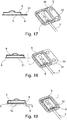
Fig. 16 ). - Eine Montage eines mit einem Foliengehäuse umschlossenen eigenständigen Optoelektronikmoduls kann auf verschiedene Weise erfolgen. Dabei überragt die zur Abdeckung der elektrischen Leiterplatte 1 verwendete Folie die Leiterplatte 1, wie in
Fig. 17 dargestellt. In diesen überragenden Teil 29 der Folie 8 können Öffnungen oder Löcher 30 eingebracht werden, in welche nicht weiter dargestellte Bolzen oder Schrauben eingeführt werden und mit denen das eigenständige Optoelektronikmodul an dem entsprechenden Ort befestigt werden kann. - In
Fig. 18 ist ein weiteres Ausführungsbeispiel dargestellt, bei welchem das eigenständige Optoelektronikmodul auf einer flexibel ausgeführten Montageplatte 31 angeordnet ist, welche ebenfalls das Optoelektronikmodul überragt und entsprechende Öffnungen 30 zur Befestigung am Verwendungsort aufweist. Die Montageplatte 31 kann mit dem Foliengehäuse verklebt oder formschlüssig verbunden sein. Wie ausFig. 19 hervorgeht, kann die Montageplatte aber auch im Folienverbund angeordnet sein, wobei die Montageplatte als Magnetplatte 32 ausgebildet ist, so dass auf mechanische Befestigungselemente zur Anbringung des eigenständig ausgebildeten Optoelektronikmoduls verzichtet werden kann. - Wie aus den
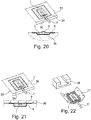
Fig. 20 und 21 hervorgeht, besteht die Möglichkeit, das Optoelektronikmodul mit den Folien auf vorgesehene Flächen 33 aufzukleben oder in dafür vorgesehene Taschen 34 in der Applikation einzusetzen. Das Aufkleben, wie es inFig. 20 dargestellt ist, erfolgt durch einen separaten Klebstoff 35 oder durch eine an dem Optoelektronikmodul befestigte selbstklebende Folie. Das Optoelektronikmodul wird so in die Applikation eingesetzt, dass es mit seiner Oberfläche die Applikation abschließt. In einer weiteren Ausführung, wie sie inFig. 21 dargestellt ist, wird das Optoelektronikmodul in der Applikation versenkt und mittels einer Abdeckfolie 36 abgedeckt, so dass eine ebene Oberfläche entsteht. - Durch die Verwendung der Folien lassen sich auch elastische Strukturen an dem Optoelektronikmodul herstellen, welche form- oder kraft- oder reibschlüssig auf die gewünschte Anwendung abgestimmt werden. So lassen sich beispielsweise, wie in
Fig. 22 gezeigt, Federelemente 37, welche durch thermisches Umformen der Folien direkt am Gehäuse erzeugt werden, herstellen, die mit einem Schwalbenschwanzprofil 38 zur Applikation harmonieren, wodurch das Optoelektronikmodul 39 nach Einführung des Federelementes 37 in das Schwalbenschwanzprofil 38 am Verwendungsort befestigt ist. - Bei der Verwendung von Kunststoff-, Teflon- oder Metallfolien ist ein Batch-Herstellungsprozess vorstellbar, bei welcher eine Vielzahl von Optoelektronikmodulen 39 auf einer Folie angeordnet wird. Anschließend wird eine zweite Folie auf die Optoelektronikmodule 39 aufgelegt. Die Verbindung der Folien in Form von Kleben oder Schweißen wird parallel durchgeführt. Nachfolgend werden die so verkapselten Optoelektronikmodule 39 via Stanz- oder Schneidevorgängen vereinzelt.
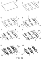
- Alternativ zu einem bereits fertigen Optoelektronikmodul 39 kann der Aufbau des Optoelektronikmoduls 39 in den Gehäuseaufbauprozess integriert werden. Dies ist in
Fig. 23 dargestellt. Hierbei werden auf eine Trägerfolie 42, beispielsweise eine Metallfolie, im Schritt I mehrere bestückte Leiterplatten 1 beabstandet aufgebracht (Schritt II). Im Schritt III erfolgt dann eine Bestückung der Leiterplatten 1 mit optoelektronischen Bauteilen 2. Im Schritt IV erfolgt die Bestückung mit Linsen 4 auf jeder Leiterplatte 1. Anschließend wird im Schritt V an jede Leiterplatte 1 eine Anschlussleitung 7 angefügt. Nach dem Anfügen der Anschlussleitung 7 an die jeweilige Leiterplatte 1 werden alle Leiterplatten 1 mit einer einzigen Deckfolie 43, die beispielsweise aus Kunststoff besteht, abgedeckt (Schritt VI). Eine Verklebung bzw. Verschweißung der Deckfolie 43 mit der Rückfolie 42 erfolgt im Schritt VII. Anschließend werden im Schritt VIII die Optoelektronikmodule 39 aus dem Verbund vereinzelt. - Als Folienmaterialien werden vorwiegend thermoplastische Materialien bevorzugt. Hinsichtlich chemischer Beständigkeit sind Teflon-Folien optimal, welche ebenfalls miteinander verschmelzt werden können. An die Folien ist neben den beschriebenen Eigenschaften die Anforderung der optischen Transparenz für die Deckfolie von besonderer Bedeutung. Außerdem sollen die Folien diffusionsdichte Eigenschaften haben. Die Folien können aber auch farbig ausgebildet werden, um Aufgaben der Spektralfilterung zu unterstützen.
- Neben der Nutzung des Verfahrens zur Ummantelung einzelner Optoelektronikmodule wäre auch der Einsatz für aneinanderhängende Sensoren denkbar, die Funktionen ähnlich eines Lichtgitters 40 bereitstellen können. Weiterführend ist auch eine mehrdimensionale Ausführung als Array-Sensor 41 denkbar, wie er in
Fig. 24 dargestellt ist. - Die beschriebenen Lösungen haben die Vorteile der Bereitstellung maximal flacher, wirtschaftlich herstellbarer und im Falle von Teflon-Folien sogar chemisch hochbeständiger Sensorgehäuse. Die Batch-Verarbeitung mehrerer Sensoren senkt dabei die Fertigungskosten.
-
- 1
- Leiterplatte
- 2
- elektronische Bauteile
- 3
- Anzeigeelement
- 4
- Linse
- 6
- Anschlusskontakt
- 7
- Leitung
- 8
- Rückseitige Folie
- 9
- Frontfolie
- 10
- Rand der Folie
- 11
- gefaltete Folie
- 12
- gespritzte Frontabdeckung
- 13
- Abstandrahmen
- 14
- Stahlblech
- 15
- Stahlblech
- 16
- Edelstahlfolie
- 17
- Edelstahlfolie
- 18
- Frontscheibe
- 19
- Isoliereinlegeteil
- 20
- Isolierplatte
- 21
- gespritztes Frontelement
- 22
- Aufkantung
- 23
- Öffnung
- 24
- Metallfolie
- 25
- Metallfolie
- 26
- Folienschlauch
- 27
- Schnittstelle: Leitungsmantel - Folie
- 28
- Bedienelement
- 29
- überragendes Teil der Folie
- 30
- Loch
- 31
- Montageplatte
- 32
- Magnetplatte
- 33
- Applikationsfläche
- 34
- Ausnehmung
- 35
- Klebstoff
- 36
- Abdeckfolie
- 37
- Federelement
- 38
- Schwalbenschwanzprofil
- 39
- Optoelektronikmodul
- 40
- Lichtgitter
- 41
- Array-Sensor
- 42
- Trägerfolie
- 43
- Deckfolie
Claims (15)
- Optoelektronikmodul, welches ein Gehäuse (8, 9; 11; 16, 17; 24, 25) aufweist, das eine bestückte Leiterplatte (1) vollständig umfasst, wobei auf der Leiterplatte (1) Sendeelemente und Empfangselemente, Sende- und Empfangslinsen (4) und elektronische Bauteile (2) zur Signalverarbeitung und eine Kontaktierung (6) für eine elektrische Leitung (7) angeordnet sind, dadurch gekennzeichnet, dass mindestens ein Teil des Gehäuses von einer reißfesten, stabilen Folie (8, 9; 11; 16, 17; 24, 25) gebildet ist, welche dicht an die bestückte Leiterplatte (1) anschließt.
- Optoelektronikmodul nach Anspruch 1, dadurch gekennzeichnet, dass die Folie (8, 9; 24, 25) aus Kunststoff oder Teflon oder Metall, vorzugsweise Edelmetall, besteht.
- Optoelektronikmodul nach Anspruch 1 oder 2, dadurch gekennzeichnet, dass das Gehäuse aus zwei Folien (8, 9) gebildet ist, die mittels Thermoumformen der Geometrie bzw. Topologie der bestückten Leiterplatte (1) angepasst ist.
- Optoelektronikmodul nach Anspruch 1 oder 2, dadurch gekennzeichnet, dass das gesamte Gehäuse aus einer gefalteten Folie (11) besteht, wobei die bestückte Leiterplatte (1) von der gefalteten Folie (11) umgeben ist, die mittels Thermoumformen der Geometrie bzw. Topologie der bestückten Leiterplatte angepasst ist.
- Optoelektronikmodul nach Anspruch 1 oder 2, dadurch gekennzeichnet, dass das Gehäuse aus einer Frontabdeckung (12) aus angespritztem Kunststoff gebildet ist, welches mit einer rückseitig auf der Frontabdeckung (12) aufgebrachten Folie (8) stoffschlüssig abgedichtet ist.
- Optoelektronikmodul nach mindestens einem der vorhergehenden Ansprüche 1 bis 4, dadurch gekennzeichnet, dass das Gehäuse aus zwei Folien (8, 9) besteht, zwischen welchen ein Abstandsrahmen (13) angeordnet ist, an welchem die beiden Folien (8, 9), diesen Abstandsrahmen (13) abdeckend, befestigt sind.
- Optoelektronikmodul nach mindestens einem der vorhergehenden Ansprüche, dadurch gekennzeichnet, dass das Gehäuse (8, 9) ein Versteifungselement (14, 15) umfasst.
- Optoelektronikmodul nach Anspruch 1 oder 2, dadurch gekennzeichnet, dass das Gehäuse (16, 17) aus einer Metallfolie (17) besteht, wobei zwischen der Metallfolie (17) und der bestückten Leiterplatte (1) ein Isoliereinlegeelement (19, 20) angeordnet ist.
- Optoelektronikmodul nach Anspruch 1, 2 oder 8, dadurch gekennzeichnet, dass das Gehäuse aus einer rückseitigen, gegenüber der bestückten Leiterplatte (1) isolierten Metallfolie (17) besteht, mit welcher eine aus einer Kunststoffabdeckung bestehende Frontseite (21) verbunden ist.
- Optoelektronikmodul nach Anspruch 1, 2, 8 oder 9, dadurch gekennzeichnet, dass die rückwärtige Metallfolie (17) zur Aufnahme der Kunststoffabdeckung (21) aufgekantet ist.
- Optoelektronikmodul nach mindestens einem der vorhergehenden Ansprüche, dadurch gekennzeichnet, dass das aus mindestens einer Kunststofffolie bestehende Gehäuse eine Ummantelung (24, 25) aus einer Metallfolie (24, 25) aufweist.
- Optoelektronikmodul nach mindestens einem der vorhergehenden Ansprüche, dadurch gekennzeichnet, dass die elektrische Leitung (7) übergangslos von dem Gehäuse (8, 9; 11; 16, 17; 24, 25) umgeben ist.
- Optoelektronikmodul nach Anspruch 1, dadurch gekennzeichnet, dass das Gehäuse durch einen Folienschlauch (26), vorteilhafterweise einen Schrumpfschlauch, gebildet ist.
- Verfahren zur Herstellung eines Optoelektronikmoduls, bei welchem optoelektronische Bauelemente und elektronische Bauteile (6) zur Signalverarbeitung und/oder eine Kontaktierung elektrisch verbunden auf einem Trägerelement (1) angeordnet werden, dadurch gekennzeichnet, dass mehrere als Leiterplatten (1) ausgebildete Trägerelemente zueinander beabstandet auf einer Folie (40) verteilt aufgebracht werden und die Trägerelemente von derselben (40) oder einer zweiten Folie (41) abgedeckt werden, wobei alle Folienränder (10) der gefalteten Folie (40) oder der ersten und der zweiten Folie (40, 41) gleichzeitig stoffschlüssig miteinander verbunden werden und die Optoelektronikmodule (39) nach der Verbindung vereinzelt werden.
- Verfahren zur Herstellung eines Optoelektronikmoduls, dadurch gekennzeichnet, dass mehrere Leiterplatten (1) beabstandet zueinander auf einer Rückfolie (42) angeordnet werden, anschließend eine Bestückung der Leiterplatten (1) mit optoelektronischen Bauelementen erfolgt, der eine Bestückung mit Linsen (4) nachfolgt und danach jede bestückte Leiterplatte (1) mit einer Anschlussleitung (7) versehen wird, wobei die mit den Anschlussleitungen (7) versehenen Leiterplatten (1) mit einer Deckfolie (43) abgedeckt werden, welche nach dem Auflegen mit der Rückfolie (42) stoffschlüssig verbunden wird und aus diesem Verbund die Optoelektronikmodule (39) vereinzelt werden.
Applications Claiming Priority (1)
| Application Number | Priority Date | Filing Date | Title |
|---|---|---|---|
| DE102017104893.6A DE102017104893B4 (de) | 2017-03-08 | 2017-03-08 | Optoelektronikmodul und Verfahren zur Herstellung eines Optoelektronikmoduls |
Publications (2)
| Publication Number | Publication Date |
|---|---|
| EP3373710A1 true EP3373710A1 (de) | 2018-09-12 |
| EP3373710B1 EP3373710B1 (de) | 2020-06-10 |
Family
ID=60972040
Family Applications (1)
| Application Number | Title | Priority Date | Filing Date |
|---|---|---|---|
| EP18151177.5A Active EP3373710B1 (de) | 2017-03-08 | 2018-01-11 | Verfahren zur herstellung eines optoelektronikmoduls |
Country Status (2)
| Country | Link |
|---|---|
| EP (1) | EP3373710B1 (de) |
| DE (1) | DE102017104893B4 (de) |
Families Citing this family (1)
| Publication number | Priority date | Publication date | Assignee | Title |
|---|---|---|---|---|
| DE102018212380A1 (de) * | 2018-07-25 | 2020-01-30 | Brose Fahrzeugteile Gmbh & Co. Kommanditgesellschaft, Bamberg | Elektronik eines Kraftfahrzeugs |
Citations (9)
| Publication number | Priority date | Publication date | Assignee | Title |
|---|---|---|---|---|
| EP0659041A1 (de) * | 1993-12-16 | 1995-06-21 | Schlegel Corporation | Abschirmung von elektromagnetischen Interferenzen mit einem flexiblen leitenden Umschlag |
| US20020036898A1 (en) * | 2000-03-29 | 2002-03-28 | Hidenori Miyakawa | Article with electronic circuit formed and method of manufacturing the same |
| WO2005060100A1 (en) * | 2003-12-16 | 2005-06-30 | Pancomp Electronics Oy | Control and user interface for electronic device |
| US20050241988A1 (en) * | 2004-04-02 | 2005-11-03 | Toshiba Matsushita Display Technology Co., Ltd. | Manufacturing method for electronic or electric products such as flat-panel display devices and band-shaped package therefor |
| DE102005008885A1 (de) * | 2005-02-26 | 2006-09-07 | Sick Ag | Optoelektronisches Verbundelement |
| GB2470350A (en) * | 2009-05-12 | 2010-11-24 | Vml Technologies Bv | Waterproof Electrical Item |
| EP2265102A1 (de) * | 2009-06-19 | 2010-12-22 | Baumer Innotec AG | Sensoraufbau ohne Gehäuse |
| DE202013004379U1 (de) * | 2013-05-13 | 2013-05-31 | Schölly Fiberoptic GmbH | Endoskop |
| US20160234944A1 (en) * | 2015-02-06 | 2016-08-11 | Masimo Corporation | Fold flex circuit for lnop |
Family Cites Families (1)
| Publication number | Priority date | Publication date | Assignee | Title |
|---|---|---|---|---|
| CN1463570A (zh) | 2001-05-25 | 2003-12-24 | 皇家菲利浦电子有限公司 | 具有在其上设置了印刷电路的印刷电路板和与所述印刷电路电连接的电部件的系统 |
-
2017
- 2017-03-08 DE DE102017104893.6A patent/DE102017104893B4/de active Active
-
2018
- 2018-01-11 EP EP18151177.5A patent/EP3373710B1/de active Active
Patent Citations (9)
| Publication number | Priority date | Publication date | Assignee | Title |
|---|---|---|---|---|
| EP0659041A1 (de) * | 1993-12-16 | 1995-06-21 | Schlegel Corporation | Abschirmung von elektromagnetischen Interferenzen mit einem flexiblen leitenden Umschlag |
| US20020036898A1 (en) * | 2000-03-29 | 2002-03-28 | Hidenori Miyakawa | Article with electronic circuit formed and method of manufacturing the same |
| WO2005060100A1 (en) * | 2003-12-16 | 2005-06-30 | Pancomp Electronics Oy | Control and user interface for electronic device |
| US20050241988A1 (en) * | 2004-04-02 | 2005-11-03 | Toshiba Matsushita Display Technology Co., Ltd. | Manufacturing method for electronic or electric products such as flat-panel display devices and band-shaped package therefor |
| DE102005008885A1 (de) * | 2005-02-26 | 2006-09-07 | Sick Ag | Optoelektronisches Verbundelement |
| GB2470350A (en) * | 2009-05-12 | 2010-11-24 | Vml Technologies Bv | Waterproof Electrical Item |
| EP2265102A1 (de) * | 2009-06-19 | 2010-12-22 | Baumer Innotec AG | Sensoraufbau ohne Gehäuse |
| DE202013004379U1 (de) * | 2013-05-13 | 2013-05-31 | Schölly Fiberoptic GmbH | Endoskop |
| US20160234944A1 (en) * | 2015-02-06 | 2016-08-11 | Masimo Corporation | Fold flex circuit for lnop |
Also Published As
| Publication number | Publication date |
|---|---|
| DE102017104893B4 (de) | 2022-01-13 |
| EP3373710B1 (de) | 2020-06-10 |
| DE102017104893A1 (de) | 2018-09-13 |
Similar Documents
| Publication | Publication Date | Title |
|---|---|---|
| DE102007059818B3 (de) | Fensterscheibe mit einem elektrischen Flachanschlusselement | |
| EP2520142B2 (de) | Sensor mit gehäuse und verfahren zu dessen herstellung | |
| AT410728B (de) | Verfahren zum einbetten zumindest einer flexiblen leiterbahnfolie in kunststoff, leiterbahneneinheitsowie einbettungseinheit hiefür | |
| DE102017130065B4 (de) | Sensorvorrichtung | |
| DE102009013111A1 (de) | Elektronische Vorrichtung | |
| DE102011085172A1 (de) | Getriebesteuermodul mit Lötbrücken oder Kaltkontakten zwischen eingesetztem Schaltungsträger und umgebendem Schaltungsträger | |
| DE102008051545A1 (de) | Elektronisches Gerät mit Mehrkontaktstecker und Verfahren zur Herstellung desselben | |
| DE102020206040A1 (de) | Antriebsvorrichtung | |
| EP1357774A1 (de) | Verfahren zum Herstellen einer kunststoffumspritzen Leiterstruktur sowie elektrische Schaltungseinheit mit einer kunststoffumspritzten Leiterstruktur | |
| EP2265102B1 (de) | Sensoraufbau ohne Gehäuse | |
| WO2011067019A1 (de) | Flexible leiterplatte sowie elektrische vorrichtung | |
| DE102008023108A1 (de) | Kantenverbinder für ein Solarmodul, Steckverbinder zur Verbindung mit dem Kantenverbinder sowie Solarmodul mit einem derartigen Kantenverbinder | |
| DE4225267C2 (de) | Abdichtungsvorrichtung für ein elektronisches Schaltgerät | |
| DE102014212296A1 (de) | Sensormodul und Verfahren zum Herstellen eines Sensormoduls | |
| EP2092218B1 (de) | Getriebesteuerung und verfahren zur montage einer getriebesteuerung | |
| DE202017101319U1 (de) | Optoelektronikmodul | |
| EP3120676B1 (de) | Elektronisches steuermodul und verfahren zu seiner herstellung | |
| EP3373710B1 (de) | Verfahren zur herstellung eines optoelektronikmoduls | |
| DE102015208486A1 (de) | Elektronische Komponente und Verfahren zu deren Herstellung | |
| DE102008058287B4 (de) | Elektronisches Modul mit einem Dichtelement und Verfahren zum Herstellen des Moduls | |
| EP2870838A2 (de) | Kraftfahrzeug-komponententräger und verfahren zu seiner herstellung | |
| EP1486388B1 (de) | Optoelektronische Sensoreinrichtung | |
| EP0744789A1 (de) | Elektrische Verbindung von einander örtlich getrennten Bauteilen | |
| EP3256820B1 (de) | Getriebesteuermodul | |
| DE102006049592A1 (de) | Steuergerät für ein Kraftfahrzeug |
Legal Events
| Date | Code | Title | Description |
|---|---|---|---|
| PUAI | Public reference made under article 153(3) epc to a published international application that has entered the european phase |
Free format text: ORIGINAL CODE: 0009012 |
|
| STAA | Information on the status of an ep patent application or granted ep patent |
Free format text: STATUS: THE APPLICATION HAS BEEN PUBLISHED |
|
| AK | Designated contracting states |
Kind code of ref document: A1 Designated state(s): AL AT BE BG CH CY CZ DE DK EE ES FI FR GB GR HR HU IE IS IT LI LT LU LV MC MK MT NL NO PL PT RO RS SE SI SK SM TR |
|
| AX | Request for extension of the european patent |
Extension state: BA ME |
|
| STAA | Information on the status of an ep patent application or granted ep patent |
Free format text: STATUS: REQUEST FOR EXAMINATION WAS MADE |
|
| 17P | Request for examination filed |
Effective date: 20190227 |
|
| RBV | Designated contracting states (corrected) |
Designated state(s): AL AT BE BG CH CY CZ DE DK EE ES FI FR GB GR HR HU IE IS IT LI LT LU LV MC MK MT NL NO PL PT RO RS SE SI SK SM TR |
|
| STAA | Information on the status of an ep patent application or granted ep patent |
Free format text: STATUS: EXAMINATION IS IN PROGRESS |
|
| 17Q | First examination report despatched |
Effective date: 20190617 |
|
| RAP1 | Party data changed (applicant data changed or rights of an application transferred) |
Owner name: SICK AG |
|
| GRAP | Despatch of communication of intention to grant a patent |
Free format text: ORIGINAL CODE: EPIDOSNIGR1 |
|
| STAA | Information on the status of an ep patent application or granted ep patent |
Free format text: STATUS: GRANT OF PATENT IS INTENDED |
|
| INTG | Intention to grant announced |
Effective date: 20200227 |
|
| GRAS | Grant fee paid |
Free format text: ORIGINAL CODE: EPIDOSNIGR3 |
|
| GRAA | (expected) grant |
Free format text: ORIGINAL CODE: 0009210 |
|
| STAA | Information on the status of an ep patent application or granted ep patent |
Free format text: STATUS: THE PATENT HAS BEEN GRANTED |
|
| AK | Designated contracting states |
Kind code of ref document: B1 Designated state(s): AL AT BE BG CH CY CZ DE DK EE ES FI FR GB GR HR HU IE IS IT LI LT LU LV MC MK MT NL NO PL PT RO RS SE SI SK SM TR |
|
| REG | Reference to a national code |
Ref country code: GB Ref legal event code: FG4D Free format text: NOT ENGLISH |
|
| REG | Reference to a national code |
Ref country code: AT Ref legal event code: REF Ref document number: 1280220 Country of ref document: AT Kind code of ref document: T Effective date: 20200615 Ref country code: CH Ref legal event code: EP |
|
| REG | Reference to a national code |
Ref country code: DE Ref legal event code: R096 Ref document number: 502018001609 Country of ref document: DE |
|
| REG | Reference to a national code |
Ref country code: IE Ref legal event code: FG4D Free format text: LANGUAGE OF EP DOCUMENT: GERMAN |
|
| REG | Reference to a national code |
Ref country code: NL Ref legal event code: FP |
|
| REG | Reference to a national code |
Ref country code: LT Ref legal event code: MG4D |
|
| PG25 | Lapsed in a contracting state [announced via postgrant information from national office to epo] |
Ref country code: FI Free format text: LAPSE BECAUSE OF FAILURE TO SUBMIT A TRANSLATION OF THE DESCRIPTION OR TO PAY THE FEE WITHIN THE PRESCRIBED TIME-LIMIT Effective date: 20200610 Ref country code: NO Free format text: LAPSE BECAUSE OF FAILURE TO SUBMIT A TRANSLATION OF THE DESCRIPTION OR TO PAY THE FEE WITHIN THE PRESCRIBED TIME-LIMIT Effective date: 20200910 Ref country code: GR Free format text: LAPSE BECAUSE OF FAILURE TO SUBMIT A TRANSLATION OF THE DESCRIPTION OR TO PAY THE FEE WITHIN THE PRESCRIBED TIME-LIMIT Effective date: 20200911 Ref country code: LT Free format text: LAPSE BECAUSE OF FAILURE TO SUBMIT A TRANSLATION OF THE DESCRIPTION OR TO PAY THE FEE WITHIN THE PRESCRIBED TIME-LIMIT Effective date: 20200610 Ref country code: SE Free format text: LAPSE BECAUSE OF FAILURE TO SUBMIT A TRANSLATION OF THE DESCRIPTION OR TO PAY THE FEE WITHIN THE PRESCRIBED TIME-LIMIT Effective date: 20200610 |
|
| PG25 | Lapsed in a contracting state [announced via postgrant information from national office to epo] |
Ref country code: RS Free format text: LAPSE BECAUSE OF FAILURE TO SUBMIT A TRANSLATION OF THE DESCRIPTION OR TO PAY THE FEE WITHIN THE PRESCRIBED TIME-LIMIT Effective date: 20200610 Ref country code: BG Free format text: LAPSE BECAUSE OF FAILURE TO SUBMIT A TRANSLATION OF THE DESCRIPTION OR TO PAY THE FEE WITHIN THE PRESCRIBED TIME-LIMIT Effective date: 20200910 Ref country code: HR Free format text: LAPSE BECAUSE OF FAILURE TO SUBMIT A TRANSLATION OF THE DESCRIPTION OR TO PAY THE FEE WITHIN THE PRESCRIBED TIME-LIMIT Effective date: 20200610 Ref country code: LV Free format text: LAPSE BECAUSE OF FAILURE TO SUBMIT A TRANSLATION OF THE DESCRIPTION OR TO PAY THE FEE WITHIN THE PRESCRIBED TIME-LIMIT Effective date: 20200610 |
|
| PG25 | Lapsed in a contracting state [announced via postgrant information from national office to epo] |
Ref country code: AL Free format text: LAPSE BECAUSE OF FAILURE TO SUBMIT A TRANSLATION OF THE DESCRIPTION OR TO PAY THE FEE WITHIN THE PRESCRIBED TIME-LIMIT Effective date: 20200610 |
|
| PG25 | Lapsed in a contracting state [announced via postgrant information from national office to epo] |
Ref country code: PT Free format text: LAPSE BECAUSE OF FAILURE TO SUBMIT A TRANSLATION OF THE DESCRIPTION OR TO PAY THE FEE WITHIN THE PRESCRIBED TIME-LIMIT Effective date: 20201012 Ref country code: RO Free format text: LAPSE BECAUSE OF FAILURE TO SUBMIT A TRANSLATION OF THE DESCRIPTION OR TO PAY THE FEE WITHIN THE PRESCRIBED TIME-LIMIT Effective date: 20200610 Ref country code: CZ Free format text: LAPSE BECAUSE OF FAILURE TO SUBMIT A TRANSLATION OF THE DESCRIPTION OR TO PAY THE FEE WITHIN THE PRESCRIBED TIME-LIMIT Effective date: 20200610 Ref country code: SM Free format text: LAPSE BECAUSE OF FAILURE TO SUBMIT A TRANSLATION OF THE DESCRIPTION OR TO PAY THE FEE WITHIN THE PRESCRIBED TIME-LIMIT Effective date: 20200610 Ref country code: EE Free format text: LAPSE BECAUSE OF FAILURE TO SUBMIT A TRANSLATION OF THE DESCRIPTION OR TO PAY THE FEE WITHIN THE PRESCRIBED TIME-LIMIT Effective date: 20200610 Ref country code: ES Free format text: LAPSE BECAUSE OF FAILURE TO SUBMIT A TRANSLATION OF THE DESCRIPTION OR TO PAY THE FEE WITHIN THE PRESCRIBED TIME-LIMIT Effective date: 20200610 |
|
| PG25 | Lapsed in a contracting state [announced via postgrant information from national office to epo] |
Ref country code: IS Free format text: LAPSE BECAUSE OF FAILURE TO SUBMIT A TRANSLATION OF THE DESCRIPTION OR TO PAY THE FEE WITHIN THE PRESCRIBED TIME-LIMIT Effective date: 20201010 Ref country code: PL Free format text: LAPSE BECAUSE OF FAILURE TO SUBMIT A TRANSLATION OF THE DESCRIPTION OR TO PAY THE FEE WITHIN THE PRESCRIBED TIME-LIMIT Effective date: 20200610 Ref country code: SK Free format text: LAPSE BECAUSE OF FAILURE TO SUBMIT A TRANSLATION OF THE DESCRIPTION OR TO PAY THE FEE WITHIN THE PRESCRIBED TIME-LIMIT Effective date: 20200610 |
|
| REG | Reference to a national code |
Ref country code: DE Ref legal event code: R097 Ref document number: 502018001609 Country of ref document: DE |
|
| PLBE | No opposition filed within time limit |
Free format text: ORIGINAL CODE: 0009261 |
|
| STAA | Information on the status of an ep patent application or granted ep patent |
Free format text: STATUS: NO OPPOSITION FILED WITHIN TIME LIMIT |
|
| PG25 | Lapsed in a contracting state [announced via postgrant information from national office to epo] |
Ref country code: DK Free format text: LAPSE BECAUSE OF FAILURE TO SUBMIT A TRANSLATION OF THE DESCRIPTION OR TO PAY THE FEE WITHIN THE PRESCRIBED TIME-LIMIT Effective date: 20200610 |
|
| 26N | No opposition filed |
Effective date: 20210311 |
|
| PG25 | Lapsed in a contracting state [announced via postgrant information from national office to epo] |
Ref country code: SI Free format text: LAPSE BECAUSE OF FAILURE TO SUBMIT A TRANSLATION OF THE DESCRIPTION OR TO PAY THE FEE WITHIN THE PRESCRIBED TIME-LIMIT Effective date: 20200610 |
|
| PG25 | Lapsed in a contracting state [announced via postgrant information from national office to epo] |
Ref country code: MC Free format text: LAPSE BECAUSE OF FAILURE TO SUBMIT A TRANSLATION OF THE DESCRIPTION OR TO PAY THE FEE WITHIN THE PRESCRIBED TIME-LIMIT Effective date: 20200610 |
|
| REG | Reference to a national code |
Ref country code: CH Ref legal event code: PL |
|
| PG25 | Lapsed in a contracting state [announced via postgrant information from national office to epo] |
Ref country code: LU Free format text: LAPSE BECAUSE OF NON-PAYMENT OF DUE FEES Effective date: 20210111 |
|
| REG | Reference to a national code |
Ref country code: BE Ref legal event code: MM Effective date: 20210131 |
|
| PG25 | Lapsed in a contracting state [announced via postgrant information from national office to epo] |
Ref country code: CH Free format text: LAPSE BECAUSE OF NON-PAYMENT OF DUE FEES Effective date: 20210131 Ref country code: LI Free format text: LAPSE BECAUSE OF NON-PAYMENT OF DUE FEES Effective date: 20210131 |
|
| PG25 | Lapsed in a contracting state [announced via postgrant information from national office to epo] |
Ref country code: IE Free format text: LAPSE BECAUSE OF NON-PAYMENT OF DUE FEES Effective date: 20210111 |
|
| PG25 | Lapsed in a contracting state [announced via postgrant information from national office to epo] |
Ref country code: BE Free format text: LAPSE BECAUSE OF NON-PAYMENT OF DUE FEES Effective date: 20210131 |
|
| GBPC | Gb: european patent ceased through non-payment of renewal fee |
Effective date: 20220111 |
|
| PG25 | Lapsed in a contracting state [announced via postgrant information from national office to epo] |
Ref country code: GB Free format text: LAPSE BECAUSE OF NON-PAYMENT OF DUE FEES Effective date: 20220111 |
|
| PG25 | Lapsed in a contracting state [announced via postgrant information from national office to epo] |
Ref country code: CY Free format text: LAPSE BECAUSE OF FAILURE TO SUBMIT A TRANSLATION OF THE DESCRIPTION OR TO PAY THE FEE WITHIN THE PRESCRIBED TIME-LIMIT Effective date: 20200610 |
|
| PG25 | Lapsed in a contracting state [announced via postgrant information from national office to epo] |
Ref country code: HU Free format text: LAPSE BECAUSE OF FAILURE TO SUBMIT A TRANSLATION OF THE DESCRIPTION OR TO PAY THE FEE WITHIN THE PRESCRIBED TIME-LIMIT; INVALID AB INITIO Effective date: 20180111 |
|
| PG25 | Lapsed in a contracting state [announced via postgrant information from national office to epo] |
Ref country code: MK Free format text: LAPSE BECAUSE OF FAILURE TO SUBMIT A TRANSLATION OF THE DESCRIPTION OR TO PAY THE FEE WITHIN THE PRESCRIBED TIME-LIMIT Effective date: 20200610 |
|
| PG25 | Lapsed in a contracting state [announced via postgrant information from national office to epo] |
Ref country code: MT Free format text: LAPSE BECAUSE OF FAILURE TO SUBMIT A TRANSLATION OF THE DESCRIPTION OR TO PAY THE FEE WITHIN THE PRESCRIBED TIME-LIMIT Effective date: 20200610 |
|
| PGFP | Annual fee paid to national office [announced via postgrant information from national office to epo] |
Ref country code: AT Payment date: 20250120 Year of fee payment: 8 |
|
| PG25 | Lapsed in a contracting state [announced via postgrant information from national office to epo] |
Ref country code: TR Free format text: LAPSE BECAUSE OF FAILURE TO SUBMIT A TRANSLATION OF THE DESCRIPTION OR TO PAY THE FEE WITHIN THE PRESCRIBED TIME-LIMIT Effective date: 20200610 |
|
| PGFP | Annual fee paid to national office [announced via postgrant information from national office to epo] |
Ref country code: NL Payment date: 20260121 Year of fee payment: 9 |
|
| PGFP | Annual fee paid to national office [announced via postgrant information from national office to epo] |
Ref country code: DE Payment date: 20260120 Year of fee payment: 9 |
|
| PGFP | Annual fee paid to national office [announced via postgrant information from national office to epo] |
Ref country code: IT Payment date: 20260130 Year of fee payment: 9 |
|
| PGFP | Annual fee paid to national office [announced via postgrant information from national office to epo] |
Ref country code: FR Payment date: 20260128 Year of fee payment: 9 |