EP3373069A1 - Pellicle for photomask, reticle including the same, and exposure apparatus for lithography - Google Patents
Pellicle for photomask, reticle including the same, and exposure apparatus for lithography Download PDFInfo
- Publication number
- EP3373069A1 EP3373069A1 EP17203361.5A EP17203361A EP3373069A1 EP 3373069 A1 EP3373069 A1 EP 3373069A1 EP 17203361 A EP17203361 A EP 17203361A EP 3373069 A1 EP3373069 A1 EP 3373069A1
- Authority
- EP
- European Patent Office
- Prior art keywords
- pellicle
- graphene
- reticle
- carbon
- photomask
- Prior art date
- Legal status (The legal status is an assumption and is not a legal conclusion. Google has not performed a legal analysis and makes no representation as to the accuracy of the status listed.)
- Granted
Links
Images








Classifications
-
- G—PHYSICS
- G03—PHOTOGRAPHY; CINEMATOGRAPHY; ANALOGOUS TECHNIQUES USING WAVES OTHER THAN OPTICAL WAVES; ELECTROGRAPHY; HOLOGRAPHY
- G03F—PHOTOMECHANICAL PRODUCTION OF TEXTURED OR PATTERNED SURFACES, e.g. FOR PRINTING, FOR PROCESSING OF SEMICONDUCTOR DEVICES; MATERIALS THEREFOR; ORIGINALS THEREFOR; APPARATUS SPECIALLY ADAPTED THEREFOR
- G03F7/00—Photomechanical, e.g. photolithographic, production of textured or patterned surfaces, e.g. printing surfaces; Materials therefor, e.g. comprising photoresists; Apparatus specially adapted therefor
- G03F7/70—Microphotolithographic exposure; Apparatus therefor
- G03F7/708—Construction of apparatus, e.g. environment aspects, hygiene aspects or materials
- G03F7/70983—Optical system protection, e.g. pellicles or removable covers for protection of mask
-
- G—PHYSICS
- G03—PHOTOGRAPHY; CINEMATOGRAPHY; ANALOGOUS TECHNIQUES USING WAVES OTHER THAN OPTICAL WAVES; ELECTROGRAPHY; HOLOGRAPHY
- G03F—PHOTOMECHANICAL PRODUCTION OF TEXTURED OR PATTERNED SURFACES, e.g. FOR PRINTING, FOR PROCESSING OF SEMICONDUCTOR DEVICES; MATERIALS THEREFOR; ORIGINALS THEREFOR; APPARATUS SPECIALLY ADAPTED THEREFOR
- G03F1/00—Originals for photomechanical production of textured or patterned surfaces, e.g., masks, photo-masks, reticles; Mask blanks or pellicles therefor; Containers specially adapted therefor; Preparation thereof
- G03F1/62—Pellicles, e.g. pellicle assemblies, e.g. having membrane on support frame; Preparation thereof
-
- G—PHYSICS
- G03—PHOTOGRAPHY; CINEMATOGRAPHY; ANALOGOUS TECHNIQUES USING WAVES OTHER THAN OPTICAL WAVES; ELECTROGRAPHY; HOLOGRAPHY
- G03F—PHOTOMECHANICAL PRODUCTION OF TEXTURED OR PATTERNED SURFACES, e.g. FOR PRINTING, FOR PROCESSING OF SEMICONDUCTOR DEVICES; MATERIALS THEREFOR; ORIGINALS THEREFOR; APPARATUS SPECIALLY ADAPTED THEREFOR
- G03F1/00—Originals for photomechanical production of textured or patterned surfaces, e.g., masks, photo-masks, reticles; Mask blanks or pellicles therefor; Containers specially adapted therefor; Preparation thereof
- G03F1/22—Masks or mask blanks for imaging by radiation of 100nm or shorter wavelength, e.g. X-ray masks, extreme ultraviolet [EUV] masks; Preparation thereof
-
- G—PHYSICS
- G03—PHOTOGRAPHY; CINEMATOGRAPHY; ANALOGOUS TECHNIQUES USING WAVES OTHER THAN OPTICAL WAVES; ELECTROGRAPHY; HOLOGRAPHY
- G03F—PHOTOMECHANICAL PRODUCTION OF TEXTURED OR PATTERNED SURFACES, e.g. FOR PRINTING, FOR PROCESSING OF SEMICONDUCTOR DEVICES; MATERIALS THEREFOR; ORIGINALS THEREFOR; APPARATUS SPECIALLY ADAPTED THEREFOR
- G03F1/00—Originals for photomechanical production of textured or patterned surfaces, e.g., masks, photo-masks, reticles; Mask blanks or pellicles therefor; Containers specially adapted therefor; Preparation thereof
- G03F1/22—Masks or mask blanks for imaging by radiation of 100nm or shorter wavelength, e.g. X-ray masks, extreme ultraviolet [EUV] masks; Preparation thereof
- G03F1/24—Reflection masks; Preparation thereof
-
- G—PHYSICS
- G03—PHOTOGRAPHY; CINEMATOGRAPHY; ANALOGOUS TECHNIQUES USING WAVES OTHER THAN OPTICAL WAVES; ELECTROGRAPHY; HOLOGRAPHY
- G03F—PHOTOMECHANICAL PRODUCTION OF TEXTURED OR PATTERNED SURFACES, e.g. FOR PRINTING, FOR PROCESSING OF SEMICONDUCTOR DEVICES; MATERIALS THEREFOR; ORIGINALS THEREFOR; APPARATUS SPECIALLY ADAPTED THEREFOR
- G03F1/00—Originals for photomechanical production of textured or patterned surfaces, e.g., masks, photo-masks, reticles; Mask blanks or pellicles therefor; Containers specially adapted therefor; Preparation thereof
- G03F1/62—Pellicles, e.g. pellicle assemblies, e.g. having membrane on support frame; Preparation thereof
- G03F1/64—Pellicles, e.g. pellicle assemblies, e.g. having membrane on support frame; Preparation thereof characterised by the frames, e.g. structure or material, including bonding means therefor
-
- G—PHYSICS
- G03—PHOTOGRAPHY; CINEMATOGRAPHY; ANALOGOUS TECHNIQUES USING WAVES OTHER THAN OPTICAL WAVES; ELECTROGRAPHY; HOLOGRAPHY
- G03F—PHOTOMECHANICAL PRODUCTION OF TEXTURED OR PATTERNED SURFACES, e.g. FOR PRINTING, FOR PROCESSING OF SEMICONDUCTOR DEVICES; MATERIALS THEREFOR; ORIGINALS THEREFOR; APPARATUS SPECIALLY ADAPTED THEREFOR
- G03F7/00—Photomechanical, e.g. photolithographic, production of textured or patterned surfaces, e.g. printing surfaces; Materials therefor, e.g. comprising photoresists; Apparatus specially adapted therefor
- G03F7/0035—Multiple processes, e.g. applying a further resist layer on an already in a previously step, processed pattern or textured surface
-
- G—PHYSICS
- G03—PHOTOGRAPHY; CINEMATOGRAPHY; ANALOGOUS TECHNIQUES USING WAVES OTHER THAN OPTICAL WAVES; ELECTROGRAPHY; HOLOGRAPHY
- G03F—PHOTOMECHANICAL PRODUCTION OF TEXTURED OR PATTERNED SURFACES, e.g. FOR PRINTING, FOR PROCESSING OF SEMICONDUCTOR DEVICES; MATERIALS THEREFOR; ORIGINALS THEREFOR; APPARATUS SPECIALLY ADAPTED THEREFOR
- G03F7/00—Photomechanical, e.g. photolithographic, production of textured or patterned surfaces, e.g. printing surfaces; Materials therefor, e.g. comprising photoresists; Apparatus specially adapted therefor
- G03F7/70—Microphotolithographic exposure; Apparatus therefor
- G03F7/70216—Mask projection systems
- G03F7/70283—Mask effects on the imaging process
-
- G—PHYSICS
- G03—PHOTOGRAPHY; CINEMATOGRAPHY; ANALOGOUS TECHNIQUES USING WAVES OTHER THAN OPTICAL WAVES; ELECTROGRAPHY; HOLOGRAPHY
- G03F—PHOTOMECHANICAL PRODUCTION OF TEXTURED OR PATTERNED SURFACES, e.g. FOR PRINTING, FOR PROCESSING OF SEMICONDUCTOR DEVICES; MATERIALS THEREFOR; ORIGINALS THEREFOR; APPARATUS SPECIALLY ADAPTED THEREFOR
- G03F7/00—Photomechanical, e.g. photolithographic, production of textured or patterned surfaces, e.g. printing surfaces; Materials therefor, e.g. comprising photoresists; Apparatus specially adapted therefor
- G03F7/70—Microphotolithographic exposure; Apparatus therefor
- G03F7/708—Construction of apparatus, e.g. environment aspects, hygiene aspects or materials
- G03F7/7095—Materials, e.g. materials for housing, stage or other support having particular properties, e.g. weight, strength, conductivity, thermal expansion coefficient
-
- G—PHYSICS
- G03—PHOTOGRAPHY; CINEMATOGRAPHY; ANALOGOUS TECHNIQUES USING WAVES OTHER THAN OPTICAL WAVES; ELECTROGRAPHY; HOLOGRAPHY
- G03F—PHOTOMECHANICAL PRODUCTION OF TEXTURED OR PATTERNED SURFACES, e.g. FOR PRINTING, FOR PROCESSING OF SEMICONDUCTOR DEVICES; MATERIALS THEREFOR; ORIGINALS THEREFOR; APPARATUS SPECIALLY ADAPTED THEREFOR
- G03F7/00—Photomechanical, e.g. photolithographic, production of textured or patterned surfaces, e.g. printing surfaces; Materials therefor, e.g. comprising photoresists; Apparatus specially adapted therefor
- G03F7/70—Microphotolithographic exposure; Apparatus therefor
- G03F7/708—Construction of apparatus, e.g. environment aspects, hygiene aspects or materials
- G03F7/7095—Materials, e.g. materials for housing, stage or other support having particular properties, e.g. weight, strength, conductivity, thermal expansion coefficient
- G03F7/70958—Optical materials or coatings, e.g. with particular transmittance, reflectance or anti-reflection properties
Definitions
- the present disclosure relates to a pellicle for a photomask, a reticle including the same, and an exposure apparatus for lithography.
- a pellicle for a photomask may be provided in the form of a film on a photomask so as to protect the photomask from external contaminants (for example, dust, resist, or the like) during optical lithography.
- Such a pellicle may have high transmittance with respect to light used in a lithography process.
- Such a pellicle may have certain characteristics such as heat dissipation characteristics, strength, uniformity, durability, stability, and the like. As features in semiconductor devices and electronic circuits have become smaller, a wavelength of light used in a lithography process may become shorter. Different pellicle materials are being developed.
- a pellicle for a photomask having high light transmittance and excellent characteristics in various aspects.
- a pellicle for a photomask having excellent durability and stability.
- a pellicle for a photomask having excellent characteristics in terms of thermal conductivity, uniformity, strength, and the like.
- a pellicle for a photomask having high transmittance and excellent resistance and durability with respect to short-wavelength light such as extreme ultraviolet (EUV) light.
- EUV extreme ultraviolet
- a reticle including the pellicle.
- a lithography apparatus to which the reticle including the pellicle is applied.
- a pellicle for protecting a photomask includes a pellicle membrane including a carbon-based material having defects and a passivation member covering the defects of the carbon-based material and including an inorganic material.
- the carbon-based material may include at least one of graphene, nanocrystalline graphene, reduced graphene oxide (rGO), carbon nanotube (CNT), fullerene, or amorphous carbon.
- the defects of the carbon-based material may include at least one of a grain boundary, a vacancy, an sp3 carbon (C) atom, an oxygen (O) atom, or a nitrogen (N) atom.
- the carbon-based material may include at least one of graphene, CNT, and fullerene, which may be formed by a growth or synthesis method, and the defects of the carbon-based material may include at least one of a grain boundary or a vacancy.
- the carbon-based material may include nanocrystalline graphene.
- a D/G intensity ratio in a Raman spectrum of the nanocrystalline graphene may be about 0.5 or more, and a 2D/G intensity ratio in the Raman spectrum of the nanocrystalline graphene may be about 0.05 or more.
- an amount of oxygen (O) in the nanocrystalline graphene may be in a range of about 1 at% to about 20 at%.
- an amount of hydrogen (H) in the nanocrystalline graphene may be in a range of about 1 at% to about 20 at%.
- an amount of nitrogen (N) in the nanocrystalline graphene may be in a range of about 1 at% to about 20 at%.
- the passivation member may include a plurality of dot elements.
- the plurality of dot elements may selectively cover the defects of the carbon-based material.
- the passivation member may have a thin film structure.
- the passivation member may be on at least one of an upper surface of the pellicle membrane or a lower surface of the pellicle membrane.
- the inorganic material of the passivation member may include at least one of a metal, an oxide, a nitride, a semiconductor, or a metal chalcogenide-based material.
- the metal may include at least one of Mo, Ti, or Ru.
- the oxide may include MoO x .
- the nitride may include at least one of TiN or SiN x .
- the semiconductor may include at least one of Ge or ZrSi 2 .
- the metal chalcogenide-based material may include a transition metal chalcogenide.
- the passivation member may have a thickness within about 20% of a thickness of the pellicle membrane.
- the passivation member may have a thickness within about 10% of a thickness of the pellicle membrane.
- the passivation member may have a thickness of about 20 nm or less.
- the passivation member may have a thickness of about 10 nm or less.
- the pellicle membrane may have a thickness of about 100 nm or less.
- each of the pellicle membrane and the passivation member may have a transmittance of about 80% or more with respect to EUV light.
- the pellicle membrane may be spaced apart from the photomask by about 1 mm to about 10 mm.
- the pellicle may further include a pellicle frame on an edge portion of the pellicle membrane.
- the pellicle may further include a bonding layer between the pellicle membrane and the pellicle frame.
- a reticle includes: a photomask; and the above-described pellicle configured to protect the photomask.
- the pellicle may be connected to the photomask.
- the reticle may be a transmissive reticle.
- the reticle may be a reflective reticle.
- the reticle may be a reticle for EUV lithography.
- an exposure apparatus for lithography includes a light source configured to generate light, and the above-discussed reticle disposed in a traveling path of the light generated by the light source.
- the exposure apparatus may further include a first optical member between the reticle and the light source and/or a second optical member between the reticle and a substrate.
- the exposure apparatus may be an EUV exposure apparatus.
- a pellicle for protecting a photomask includes a pellicle membrane, a frame, and a passivation member.
- the pellicle membrane includes a carbon-based material.
- the carbon-based material has defects.
- the frame supports the pellicle membrane.
- the passivation member may be on top of at least one of the frame and the pellicle membrane.
- the passivation member covers the defects of the carbon-based material.
- the passivation member includes an inorganic material.
- the carbon-based material may include at least one of graphene, nanocrystalline graphene, reduced graphene oxide (rGO), carbon nanotube (CNT), fullerene, or amorphous carbon.
- the passivation layer may include a first passivation layer and a second passivation layer.
- the first passivation layer may be between the frame and the pellicle membrane.
- the second passivation layer may be on top of the pellicle membrane and the frame.
- the inorganic material may include at least one of MoO x , TiN, SiN x , Ge, ZrSi 2 , or a transition metal chalcogenide.
- a reticle may include the photomask and the above-discussed pellicle.
- the pellicle may be connected to the photomask and configured to protect the photomask.
- an exposure apparatus for lithography includes a light source configured to generate light, and the above-discussed reticle disposed in a traveling path of the light generated by the light source.
- first, second, etc. may be used herein to describe various elements, components, regions, layers and/or sections, these elements, components, regions, layers and/or sections should not be limited by these terms. These terms are only used to distinguish one element, component, region, layer or section from another element, component, region, layer or section. Thus, a first element, component, region, layer or section discussed below could be termed a second element, component, region, layer or section without departing from the teachings of example embodiments.
- spatially relative terms such as “beneath,” “below,” “lower,” “above,” “upper” and the like, may be used herein for ease of description to describe one element or feature's relationship to another element(s) or feature(s) as illustrated in the figures. It will be understood that the spatially relative terms are intended to encompass different orientations of the device in use or operation in addition to the orientation depicted in the figures. For example, if the device in the figures is turned over, elements described as “below” or “beneath” other elements or features would then be oriented “above” the other elements or features. Thus, the term “below” can encompass both an orientation of above and below. The device may be otherwise oriented (rotated 90 degrees or at other orientations) and the spatially relative descriptors used herein interpreted accordingly.
- Example embodiments are described herein with reference to cross-sectional illustrations that are schematic illustrations of idealized embodiments (and intermediate structures) of example embodiments. As such, variations from the shapes of the illustrations as a result, for example, of manufacturing techniques and/or tolerances, are to be expected. Thus, example embodiments should not be construed as limited to the particular shapes of regions illustrated herein but are to include deviations in shapes that result, for example, from manufacturing. For example, an implanted region illustrated as a rectangle will, typically, have rounded or curved features and/or a gradient of implant concentration at its edges rather than a binary change from implanted to non-implanted region.
- a buried region formed by implantation may result in some implantation in the region between the buried region and the surface through which the implantation takes place.
- the regions illustrated in the figures are schematic in nature and their shapes are not intended to illustrate the actual shape of a region of a device and are not intended to limit the scope of example embodiments.
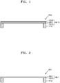
- FIG. 1 is a cross-sectional view of a pellicle P10 for a photomask, according to some example embodiments.
- the pellicle P10 may include a pellicle membrane M10.
- the pellicle membrane M10 may include a carbon-based material having defects.
- a constituent material (or a main constituent material) of the pellicle membrane M10 may be a carbon-based material.
- the carbon-based material may include a two-dimensional (2D) carbon structure or a carbon-based nanomaterial.
- the carbon-based material may include at least one selected from graphene, nanocrystalline graphene, reduced graphene oxide (rGO), carbon nanotube (CNT), fullerene, and amorphous carbon.
- the defects of the carbon-based material may include at least one selected from an sp3 carbon (C) atom, an oxygen (O) atom, a nitrogen (N) atom, and a carbon vacancy. Also, the defects may have various forms, for example, a point defect or a line defect such as a grain boundary.
- the pellicle P10 may include at least one passivation member, for example, passivation members PS10 and PS20 covering the defects of the carbon-based material.
- the at least one passivation member may be disposed on at least one of a first surface (e.g., a lower surface) and a second surface (e.g., an upper surface) of the pellicle membrane M10.
- FIG. 1 illustrates a case where the first passivation member PS10 is disposed on the lower surface of the pellicle membrane M10, and the second passivation member PS20 is disposed on the upper surface of the pellicle membrane M10.
- Each of the passivation members PS10 and PS20 may include an inorganic material.
- the passivation members PS10 and PS20 may serve to suppress or prevent a problem in which characteristics of the pellicle membrane M10 are degraded by light or gas.
- the light may include extreme ultraviolet (EUV) light
- the gas may include H 2 .
- the inorganic material may be a material that is stable in an environment in which EUV energy or H 2 gas is used. Therefore, the passivation members PS10 and PS20 including the inorganic material may serve to suppress or prevent the pellicle membrane M10 from being degenerated or degraded by light or gas. In particular, defective regions of the pellicle membrane M10 may be degenerated or degraded relatively easily. Due to the use of the passivation members PS10 and PS20, such a problem may be suppressed or prevented.
- the inorganic material of the passivation members PS10 and PS20 may be a material that has high transmittance and excellent resistance and durability with respect to short-wavelength light such as EUV light.
- the inorganic material may be a material that has relatively excellent strength and uniformity and is prepared by a relatively simple method.
- the inorganic material may include at least one selected from a metal, an oxide, a nitride, a semiconductor, and a metal chalcogenide-based material.
- the metal may include at least one selected from Mo, Ti, and Ru.
- the oxide may be a metal oxide and may include, for example, molybdenum oxide (MoO x ).
- the nitride may be a metal nitride or a non-metal nitride and may include, for example, at least one selected from titanium nitride (TiN) and silicon nitride (SiN x ).
- the semiconductor may include, for example, at least one selected from Ge and zirconium silicide (e.g., ZrSi 2 ).
- the metal chalcogenide-based material may include a transition metal chalcogenide, and the transition metal chalcogenide may include a transition metal dichalcogenide (TMD).
- TMD transition metal dichalcogenide
- the metal may further include Zr or the like
- the semiconductor may further include Si or the like.
- Various other materials may be applied to the passivation members PS10 and PS20.
- the passivation members PS10 and PS20 may include the same material or may include at least one different material from each other.
- the pellicle membrane M10 may have a thickness of greater than 0 nm and about 100 nm or less.
- the pellicle membrane M10 may have a thickness of about 70 nm or less, or about 50 nm or less.
- the pellicle membrane M10 may have a transmittance of about 80% or more, or about 90% or more, with respect to EUV light.
- Each of the first and second passivation members PS10 and PS20 may have a thickness less than that of the pellicle membrane M10.
- each of the first and second passivation members PS10 and PS20 may have a thickness within about 20% or about 10% of a thickness of the pellicle membrane M10.
- each of the first and second passivation members PS10 and PS20 may have a thickness of about 20 nm or less, about 10 nm or less, or about 5 nm or less.
- Each of the first and second passivation members PS10 and PS20 may have a transmittance of about 80% or more, or about 90% or more, with respect to EUV light.
- Each of the first and second passivation members PS10 and PS20 may have a transmittance that is less than or equal to about 100% with respect to EUV light.
- a case where each of the first and second passivation members PS10 and PS20 has a thickness less than that of the pellicle membrane M10 is advantageous in securing transmittance and thickness uniformity.
- At least one of the first and second passivation members PS10 and PS20 may be a thin film-type passivation member or an island-type passivation member including a plurality of dot elements.
- the pellicle membrane M10 and the passivation members PS10 and PS20 may be collectively referred to as a membrane layer ML10. That is, the pellicle membrane M10 and the passivation members PS10 and PS20 may constitute the membrane layer ML10.
- the membrane layer ML10 may be referred to as a "membrane structure".
- the membrane layer ML10 may have a transmittance of about 80% or more, or about 90% or more, with respect to EUV light.
- the pellicle P10 may further include a pellicle frame F10 so as to support the pellicle membrane M10. Due to the pellicle frame F10, the pellicle membrane M10 may be spaced apart from a photomask (not illustrated) by a certain interval.
- the pellicle frame F10 may be disposed at an edge portion of the pellicle membrane M10. When viewed from above, the pellicle frame F10 may have a rectangular or circular frame structure or other various shapes.
- the first passivation member PS10 may be disposed between the pellicle membrane M10 and the pellicle frame F10. In a process of forming the pellicle frame F10, the first passivation member PS10 may serve to protect the pellicle membrane M10.
- first and second passivation members PS10 and PS20 are disposed on two sides of the pellicle membrane M10 is illustrated in FIG. 1 , but in some embodiments, one of the passivation members may be disposed at only one side of the pellicle membrane M10. Examples thereof are illustrated in FIGS. 2 and 3 .
- the passivation member PS10 may be disposed on one surface of the pellicle membrane M10, for example, the lower surface of the pellicle membrane M10.
- the passivation member PS20 may be disposed on another surface of the pellicle membrane M10, for example, the upper surface of the pellicle membrane M10. Even though the passivation member PS10 or PS20 is disposed on only one side of the pellicle membrane M10, the passivation member PS10 or P20 may protect the pellicle membrane M10.
- the pellicle membrane M10 and the passivation member PS10 may constitute a membrane layer ML11, and the membrane layer ML11 and the pellicle frame F10 may constitute a pellicle P11 for a photomask.
- the pellicle membrane M10 and the passivation member PS20 may constitute a membrane layer ML12, and the membrane layer ML12 and the pellicle frame F10 may constitute a pellicle P12 for a photomask.
- FIG. 4 is a cross-sectional view of a pellicle P1 for a photomask, according to a comparative example.
- the pellicle P1 according to the comparative example may include a pellicle membrane GL1 including a graphene layer. That is, the pellicle membrane GL1 may be a graphene layer.
- the pellicle membrane GL1 may not include the passivation members PS10 and PS20 described above with reference to FIGS. 1 to 3 .
- a pellicle frame F1 supports the pellicle membrane GL1.
- the pellicle P1 of FIG. 4 according to the comparative example When the pellicle P1 of FIG. 4 according to the comparative example is used, the pellicle P1 may be easily degenerated and degraded by EUV light or EUV light + H 2 . This will be described below with reference to FIG. 5 .
- FIG. 5 shows a result of Raman spectroscopy analysis of a change in properties when the pellicle P1 according to the comparative example was exposed to EUV light and EUV light + H 2 .
- FIG. 5 shows Raman spectroscopy plots of a case where the pellicle P1 was in a pristine state, a case where the pellicle P1 was exposed to EUV light, and a case where the pellicle P1 was exposed to EUV light + H 2 .
- D peak is a peak appearing at about 1,340 cm -1 to about 1,350 cm -1
- G peak is a peak appearing at about 1,580 cm -1
- 2D peak is a peak appearing at about 2,700 cm -1 .
- the heights and ratios of peaks were changed in the case of exposure to EUV light and EUV light + H 2 , as compared with the pristine state.
- the D peak changed greatly.
- the height of the D peak was increased, and in the case of exposure to EUV light + H 2 , the height of the D peak was more greatly increased.
- the pellicle membrane (graphene layer) As the pellicle membrane (graphene layer) is exposed to EUV light and EUV light + H 2 , the pellicle membrane (graphene layer) may be gradually etched and characteristics of the pellicle membrane (graphene layer), such as transmittance, may be changed. Such a problem may be caused by a defective region of the pellicle membrane (graphene layer).
- FIG. 6 is a diagram illustrating a case where a fluorine (F) atom is adsorbed onto an internal region other than a graphene edge and then migrates.
- the fluorine (F) atom may be adsorbed onto the internal region other than the graphene edge and may not migrate easily. Energy required for the migration of the fluorine (F) atom may be about 5.5 kcal/mol or more. Therefore, the internal region of graphene may have very low reactivity. In other words, the internal region of graphene may have relatively excellent stability.
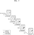
- FIG. 7 is a diagram illustrating a case where a fluorine atom is adsorbed onto a graphene edge portion and then undergoes a reaction.
- the fluorine (F) atom may be well adsorbed onto the graphene edge portion and undergo a reaction.
- Energy required to change from an (a) state to a (b) state may be about -51.7 kcal/mol.
- the (a) state is a state in which no fluorine (F) atom is adsorbed onto a graphene edge
- the (b) state is a state in which one fluorine (F) atom is adsorbed onto a graphene edge. That the energy required to change from the (a) state to the (b) state is a negative (-) value means that such a reaction can easily occur.
- Energy required to change from the (b) state to a (c) state, from the (c) state to a (d) state, from the (d) state to an (e) state, and from the (e) state to an (f) state may all have a negative value.
- breakage of C-C bonds occurs in the process of changing from the (c) state to the (d) state.
- Energy required at this time may be about -46.4 kcal/mol, and this may be an exothermic reaction.
- the graphene edge region e.g., the defective region, may have relatively high reactivity with an external atom, and degeneration and degradation may easily progress therein.
- FIGS. 6 and 7 illustrate an example in which the fluorine (F) atom is adsorbed and undergoes a reaction, and a type of an atom that is adsorbed and undergoes a reaction may be variously changed. Also, the positive (+) or negative (-) energies described with reference to FIGS. 6 and 7 are based on simulation and may be different from actual energies.
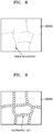
- FIG. 8 is a plan view illustrating an example of a planar form of a graphene layer.
- the graphene layer may have a plurality of crystal grains and a grain boundary therebetween.
- the grain boundary may be a type of a graphene edge.
- the graphene layer may not have a monocrystalline structure as a whole and may include a plurality of crystal grains and a grain boundary therebetween.
- FIG. 9 is a plan view illustrating an example in which a plurality of dot elements covering the grain boundary are formed on the graphene layer of FIG. 8 .
- the dot elements covering the grain boundary may be formed on the graphene layer.
- the dot elements may include an inorganic material and may be formed along the grain boundary.
- the dot elements may be an example of the passivation member PS10 or PS20 described above with reference to FIG. 1 .
- the dot elements may selectively cover the defective region of the graphene layer, that is, the grain boundary.
- the dot elements since the internal region of graphene of the graphene layer has hydrophobicity and low reactivity and the grain boundary region has relatively high reactivity, the dot elements may be formed along the grain boundary region. These dot elements may serve to protect the graphene layer from light and gas used in a lithography process.
- Each of the dot elements may have a size (diameter) of tens of nm or less, but in some embodiments, may have a size (diameter) of about 100 nm or more.
- FIG. 10 is a scanning electron microscope (SEM) image showing a case where a plurality of dot elements are formed on a graphene layer along a grain boundary.
- a plurality of inorganic dots may be formed along a graphene edge, that is, a grain boundary.
- the passivation member may not be a multi-dot type but a thin film type. One example thereof is illustrated in FIG. 11 .
- FIG. 11 is a cross-sectional view for describing a pellicle for a photomask, according to some example embodiments.
- the pellicle may include thin film-type passivation layers PS11 and PS22 on a graphene layer GL10.
- the passivation layers PS11 and PS22 may be disposed on one or two surfaces of the graphene layer GL10.
- FIG. 11 illustrates a case where first and second passivation layers PS11 and PS22 are disposed on two surfaces of the graphene layer GL10.
- the passivation layers PS11 and PS22 may have a continuous layer shape.
- the thin film-type passivation layers PS11 and PS22 may be formed according to a process or condition for forming the passivation layers PS11 and PS22.
- Each of the passivation layers PS11 and PS22 may have a thickness less than that of the graphene layer GL10.
- Each of the passivation layers PS11 and PS22 may have a thickness within about 20% or about 10% of a thickness of the graphene layer GL10.
- each of the passivation layers PS11 and PS22 may have a thickness of about 20 nm or less, about 10 nm or less, or about 5 nm or less.
- the graphene layer GL10 may be an example of the pellicle membrane.
- a carbon-based material formed by a growth or synthesis method may include defects.
- graphene, CNT, or fullerene formed by the growth or synthesis method may have defects such as a grain boundary or a vacancy.
- the vacancy may be a carbon vacancy.
- the carbon-based material formed by the growth or synthesis method may include, as the defects, at least one selected from an oxygen (O) atom, a nitrogen (N) atom, and a hydrogen (H) atom.
- acid treatment may be performed in a refining process after synthesis, and defects may be generated by the acid treatment.
- the passivation members PS11 and PS22 may include the same material or may include at least one different material from each other.
- the passivation members may be formed by using a deposition process or a solution process.
- the deposition process may be chemical vapor deposition (CVD), atomic layer deposition (ALD), or physical vapor deposition (PVD).
- the solution process may be performed by coating a solution including a source material on a membrane (for example, a graphene layer) and performing a drying and/or annealing process thereon.
- the coating method may be, for example, spin coating.
- Dot-type passivation members or thin film-type passivation members may be formed according to a type or a specific condition of the deposition process or the solution process. For example, since the internal region of graphene of the membrane (e.g., the graphene layer) has hydrophobicity and low reactivity and the grain boundary region has relatively high reactivity, the dot-type passivation member may be formed along the grain boundary region. Also, dot-type passivation members or thin film-type passivation members may be formed according to a concentration of the source material included in the solution used in the solution process. However, the above-described method of forming the passivation members is merely an example and may be changed.
- the pellicle membranes M10 of FIGS. 1 to 3 may include, for example, nanocrystalline graphene.
- nanocrystalline graphene which may be included in the pellicle membrane M10, will be described in detail with reference to FIGS. 12 and 13A to 13E .
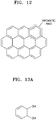
- FIG. 12 illustrates a chemical structure of a crystal grain of nanocrystalline graphene applicable to a pellicle membrane M10 of FIGS. 1 to 3 .
- the crystal grain does not include any defects, but an actual crystal grain may include defect(s).
- the crystal grain may include a "2D carbon structure" having an aromatic ring structure. Carbon atoms may form an aromatic ring structure, and such ring structures (annular structures) may be two-dimensionally arranged.
- a size of the crystal grain may be nanoscale. A size (length/diameter) of the crystal grain may be several hundreds of nm or less, for example, about 100 nm or less.
- the size, shape, and structure of the crystal grain illustrated in FIG. 12 are merely examples and may be variously changed. Possible defects of the crystal grain will be described with reference to FIGS. 13A to 13E .
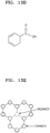
- FIGS. 13A to 13E illustrate chemical structures for describing various possible defects of the nanocrystalline graphene applicable to the pellicle membrane M10 of FIGS. 1 to 3 .
- FIGS. 13A to 13E illustrate possible defects of the crystal grain of FIG. 12 .
- FIG. 13A illustrates a case where some carbon atoms forming an aromatic ring structure become sp3 carbons when double bonds thereof are broken, and hydroxy groups (OH) are bonded to the sp3 carbons.
- Carbon atoms maintaining double bonds in the aromatic ring structure may be referred to as sp2 carbons. Since all carbon atoms constituting general graphene may be sp2 carbons, the sp3 carbons may be regarded as defects of graphene. Also, a functional group (or a substituent) such as the hydroxy group (OH) bonded to the sp3 carbon may be regarded as defects.
- FIG. 13B illustrates a case where some carbon atoms forming an aromatic ring structure become sp3 carbons when double bonds thereof are broken, and an oxygen (O) atom is bonded to the sp3 carbons.
- the oxygen (O) atom may be bonded to two adjacent sp3 carbons.
- Such an oxygen (O) atom may be referred to as an epoxy group.
- FIG. 13C illustrates a case where some carbon atoms forming an aromatic ring structure become sp3 carbons when double bonds thereof are broken, and hydrogen (H) atoms are bonded to the sp3 carbons.
- a hydrogen (H) atom may be bonded to one of the two adjacent sp3 carbons, and a hydroxy group (OH) may be bonded to the other.
- FIG. 13E illustrates a case where a carbon vacancy is generated in a 2D carbon structure having an aromatic ring structure. It can be said that FIGS. 13A to 13D illustrate a case where a functional group (or a substituent) or other atoms (atoms except for carbon) are bonded to the sp3 carbon, and FIG. 13E illustrates a case where a carbon vacancy is generated without a functional group (or a substituent).
- the defects described with reference to FIGS. 13A to 13E may be applied to the crystal grain illustrated in FIG. 12 .
- various types of defects may be included in the nanocrystalline graphene constituting the pellicle membrane M10 of FIGS. 1 to 3 .
- the defects may include a nitrogen (N) atom.
- the nitrogen atom may be bonded to the sp3 carbon in the form of NH 2 .
- NH 2 instead of OH may be bonded to the sp3 carbon.
- At least two of the nitrogen atom and the various types of defects described with reference to FIGS. 13A to 13E may be included in one nanocrystalline graphene or one crystal grain. Also, defects other than the above-described defects may be present.
- Defects of the nanocrystalline graphene may include at least one selected from an sp3 carbon atom, an oxygen atom, a nitrogen atom, and a carbon vacancy.
- the oxygen atom may be the oxygen atom included in OH of FIG. 13A , the oxygen atom of FIG. 13B , or the oxygen atom included in COOH of FIG. 13D , or may also be present in various forms.
- the nitrogen atom may be included in the form of, for example, NH 2 , or may also be included in various forms.
- the hydrogen (H) atoms included OH of FIG. 13A , H of FIG. 13C , and COOH of FIG. 13D may be regarded as defects.
- An amount (content) of hydrogen (H) in the nanocrystalline graphene may be larger than that in general graphene (for example, monocrystalline graphene).
- general graphene for example, monocrystalline graphene
- a very small amount of hydrogen (H) may be present only at the edge portion.
- An amount of hydrogen (H) in the nanocrystalline graphene may be larger than that in the monocrystalline graphene.
- an amount of hydrogen (H) in the nanocrystalline graphene may be smaller than that in an amorphous carbon layer (ACL).
- An amount of hydrogen (H) in the ACL may be about 23.6 at%, and an amount of hydrogen (H) in the nanocrystalline graphene may be smaller than about 23.6 at%.
- An amount (content) of oxygen (O) in the nanocrystalline graphene described with reference to FIGS. 1 to 13E may be in a range of about 12 at% to about 40 at%.
- an amount of oxygen (O) in the nanocrystalline graphene may be in a range of about 1 at% to about 20 at%, or about 1 at% to about 10 at%.
- An amount (content) of hydrogen (H) in the nanocrystalline graphene may be in a range of about 1 at% to about 25 at%.
- an amount of hydrogen (H) in the nanocrystalline graphene may be in a range of about 1 at% to about 20 at%.
- an amount (content) of nitrogen (N) in the nanocrystalline graphene may be in a range of about 1 at% to about 30 at%.
- an amount of nitrogen (N) in the nanocrystalline graphene may be in a range of about 1 at% to about 20 at%.
- the nanocrystalline graphene may contain about 1 at% or less of nitrogen (N) or may not contain nitrogen (N).
- an intensity ratio of D peak to G peak may be about 0.5 or more.
- the G peak is a peak appearing at about 1,580 cm -1 .
- the G peak may be caused in a vibration mode corresponding to stretching of a carbon-carbon bond and provide information capable of determining the inclusion or non-inclusion of an aromatic ring structure.
- the D peak is a peak appearing in a range of about 1,340 cm -1 to about 1,350 cm -1 .
- the D peak may be generated by defects such as an sp3 carbon and a carbon vacancy.
- the D/G intensity ratio may be about 0.5 or more.
- the D/G intensity ratio may be about 1 or more.
- the D/G intensity ratio may be about 2 or less.
- an intensity ratio of 2D peak to G peak may be about 0.05 or more.
- the 2D peak is a peak appearing at about 2,700 cm -1 and provides information capable of determining an amount of an aromatic ring structure.
- the 2D/G intensity ratio may be about 0.05 or more.
- the 2D/G intensity ratio may be about 0.1 or more.
- the 2D/G intensity ratio may be about 1 or less. However, in some cases, the 2D/G intensity ratio may be greater than about 1.
- FIG. 14 is a cross-sectional view for describing a layer structure of nanocrystalline graphene NG11 applicable to a pellicle membrane for a photomask, according to some example embodiments.
- the nanocrystalline graphene NG11 applicable to the pellicle may include a plurality of crystal grains G11.
- a size (length/diameter) of each of the crystal grains G11 may be several hundreds of nm or less, for example, about 100 nm or less.
- the crystal grains G11 may be roughly arranged (aligned) in a direction parallel to the nanocrystalline graphene NG11.
- the nanocrystalline graphene NG11 may have an irregular lattice structure in a vertical direction, that is, a C-axis direction. In other words, the crystal grains G11 may not have a regular or ordered lattice structure, such as graphite, in the C-axis direction.
- the crystal grains G11 may have a regular (or relatively regular) lattice structure in the C-axis direction in some regions of the nanocrystalline graphene NG11. Even in this case, the crystal grains G11 may have an irregular lattice structure in the C-axis direction in another region of the nanocrystalline graphene NG11. Therefore, when taking into account the entire regions, the nanocrystalline graphene NG11 may be said to have an irregular lattice structure in the C-axis direction.
- An interlayer spacing, e.g., a d-spacing of the nanocrystalline graphene NG11 may be greater than a d-spacing of graphite.
- the d-spacing of the nanocrystalline graphene NG11 may be greater than about 3.35 ⁇ .
- the d-spacing of the nanocrystalline graphene NG11 may be about 3.4 ⁇ or more.
- the d-spacing may be obtained by X-ray diffraction analysis.
- the nanocrystalline graphene NG11 may have an increased d-spacing since the nanocrystalline graphene NG11 has a nanocrystalline structure and includes defects.
- FIG. 15 is a cross-sectional view for describing a layer structure of nanocrystalline graphene NG12 applicable to a pellicle membrane for a photomask, according to some example embodiments.
- the nanocrystalline graphene NG12 applicable to the pellicle may include a plurality of crystal grains G12.
- a size (length/diameter) of each of the crystal grains G12 may be several hundreds of nm or less, for example, about 100 nm or less.
- the crystal grains G12 may be arranged in a random direction or a relatively random direction. Therefore, the nanocrystalline graphene NG12 may have an irregular lattice structure in a C-axis direction. However, the crystal grains G12 may have a regular (or relatively regular) lattice structure in the C-axis direction in some regions (fine regions) of the nanocrystalline graphene NG12.
- a d-spacing of the nanocrystalline graphene NG12 may be greater than about 3.35 ⁇ .
- the d-spacing of the nanocrystalline graphene NG12 may be about 3.4 ⁇ or more.
- a density of the nanocrystalline graphenes NG11 and NG12 may be less than a density of graphite.
- the density of the nanocrystalline graphenes NG11 and NG12 may be less than about 2.2 g/cm 3 .
- the density of the nanocrystalline graphenes NG11 and NG12 may be less than about 2.15 g/cm 3 .
- the density of the nanocrystalline graphenes NG11 and NG12 may be less than about 2.0 g/cm 3 .
- the density of the nanocrystalline graphenes NG11 and NG12 may be greater than a density of an amorphous carbon layer (ACL).
- ACL amorphous carbon layer
- the density of the nanocrystalline graphenes NG11 and NG12 may be greater than about 1.5 g/cm 3 .
- the density of the nanocrystalline graphenes NG11 and NG12 may be greater than about 1.5 g/cm 3 and less than about 2.2 g/cm 3 .
- the layer structures of the nanocrystalline graphenes NG11 and NG12 described with reference to FIGS. 14 and 15 are merely examples and may be variously changed.
- the structures of FIGS. 14 and 15 may be mixed.
- one of a lower layer region and an upper layer region of one nanocrystalline graphene may have the structure of FIG. 14
- the other may have the structure of FIG. 15 .
- Other various structures may be applied to the nanocrystalline graphenes NG11 and NG12.
- the nanocrystalline graphenes NG11 and NG12 may be formed by using various methods.
- the nanocrystalline graphenes NG11 and NG12 may be formed by using a deposition process, such as chemical vapor deposition (CVD) or a solution process using a graphene-containing solution.
- CVD chemical vapor deposition
- a solution process using a graphene-containing solution a deposition process using a graphene-containing solution.
- Nanocrystalline graphene may be formed by using the deposition process such as CVD.
- the CVD may be thermal CVD or plasma CVD.
- Examples of the plasma CVD may include inductively coupled plasma CVD (ICP-CVD) and plasma enhanced CVD (PE-CVD).
- the CVD may use a gas source or a solid source (for example, a source of carbon).
- the solid source may include polymer, organic monomer, or the like.
- the nanocrystalline graphene may be formed by adjusting a type (material) of a substrate and a process temperature (deposition temperature) in the deposition process. Also, in forming the nanocrystalline graphene, an amount or type of defects included in the nanocrystalline graphene may be adjusted by additionally using defect-causing materials.
- the nanocrystalline graphene has crystallinity.
- the crystallinity of the nanocrystalline graphene NG1 may be lower than that of graphite or monocrystalline graphene.
- various characteristics may be exhibited by defects included in the nanocrystalline graphene.
- a graphene-containing solution may be prepared by dissolving graphene particles, each having a size of several tens of nm or less, in a certain solvent.
- a film may be formed by coating the solution on a certain substrate (underlayer).
- nanocrystalline graphene may be formed from the film by performing annealing or heat treatment on the film.
- the graphene particles may be graphene quantum dots (GQDs) or graphene nanoplates.
- graphene oxide particles may be used instead of the graphene particles or together with the graphene particles.
- the solvent may include at least one selected from N-methylpyrrolidone (NMP), dimethylformamide (DMF), and NH 4 OH, but inventive concepts are not limited thereto.
- the process of coating the solvent on the substrate (underlayer) may be performed by using various coating methods or film casting methods.
- the annealing or heat treatment may be performed on the film coated on the substrate (underlayer) at a temperature lower than about 2,000°C.
- the annealing or heat treatment may be performed at a temperature of about 1,200°C or lower, but may be performed at a temperature higher than about 1,200°C.
- the nanocrystalline graphene may be formed in the above-described manner. Crystallinity or defects of the nanocrystalline graphene may be adjusted by controlling the temperature or atmosphere of the annealing or heat treatment. In some cases, defect-causing materials may be additionally used.
- the nanocrystalline graphene formed in the above-described manner may have excellent uniformity.
- the nanocrystalline graphene may have excellent thickness uniformity and surface uniformity.
- the surface roughness of the nanocrystalline graphene may be less than about 10 nm.
- the surface roughness of the nanocrystalline graphene may be about 6 nm or less, or about 3 nm or less.
- the nanocrystalline graphene may show uniform light transmittance as a whole. Therefore, when the nanocrystalline graphene is used in a pellicle membrane for lithography, uniformity and precision of the lithography process may be easily secured.
- the nanocrystalline graphene may have high transmittance with respect to a certain wavelength range of light.
- the nanocrystalline graphene may have a transmittance of about 80% or more, or about 90% or more, with respect to extreme ultraviolet (EUV) light.
- EUV extreme ultraviolet
- the nanocrystalline graphene may have a transmittance of about 80% or more, or about 90% or more, with respect to EUV light in a thickness range of about 5 nm to about 100 nm.
- the nanocrystalline graphene may be usefully applied to an EUV lithography apparatus.
- the nanocrystalline graphene may have high thermal conductivity, excellent heat dissipation characteristics, excellent EUV resistance, and excellent mechanical strength (tensile strength).
- the nanocrystalline graphene may have an in-plane thermal conductivity of several thousands of W/m ⁇ k, a Young's modulus of several hundreds of GPa or more, and a tensile strength of several tens of GPa or more, or about 100 GPa or more.
- the nanocrystalline graphene may have excellent characteristics as a material of the pellicle membrane in various aspects. Also, the nanocrystalline graphene may have excellent durability and stability.
- the nanocrystalline graphene When the nanocrystalline graphene is applied to the pellicle membrane M10 of FIGS. 1 to 3 , the nanocrystalline graphene may have a thickness of about 100 nm or less. In other words, the pellicle membrane M10 including the nanocrystalline graphene may have a thickness of about 100 nm or less. For example, the nanocrystalline graphene may have a thickness of about 50 nm or less. The nanocrystalline graphene may have a transmittance of about 80% or more, or about 90% or more, with respect to EUV light.
- FIG. 16 is a graph showing a result of Raman spectroscopy analysis of nanocrystalline graphene, according to embodiments.
- nanocrystalline graphene ncG1 and nanocrystalline graphene ncG2 were formed by a deposition process.
- the nanocrystalline graphene ncG1 differs from the nanocrystalline graphene ncG2 in terms of a process temperature.
- the nanocrystalline graphene ncG1 was formed at a process temperature of 560°C, and the nanocrystalline graphene ncG2 was formed at a process temperature of 590°C.
- a D/G intensity ratio may be about 0.5 or more.
- the D/G intensity ratio may be about 1 or more.
- the D/G intensity ratio may be about 2 or less.
- a 2D/G intensity ratio may be about 0.05 or more.
- the 2D/G intensity ratio may be about 0.1 or more.
- the 2D/G intensity ratio may be about 1 or less.
- FIG. 17 is a graph showing a result of X-ray diffraction analysis of nanocrystalline graphenes, according to embodiments.
- 2 ⁇ or the like at which the peak appears may be obtained.
- an interlayer spacing e.g., d-spacing (d002)
- d-spacing d002
- a d-spacing of the nanocrystalline graphene may be greater than about 3.35 ⁇ .
- the d-spacing of the nanocrystalline graphene may be 3.4 ⁇ or more.
- the nanocrystalline graphene which may be included in the pellicle membrane (M10 in FIGS. 1 to 3 ), has been illustrated and described in FIGS. 12 to 17 , but the pellicle membrane M10 may include graphene other than the nanocrystalline graphene, or may include rGO, CNT, fullerene, amorphous carbon, or the like.
- the graphene other than the nanocrystalline graphene may be monocrystalline graphene or polycrystalline graphene.
- the monocrystalline graphene or the polycrystalline graphene may have thermal conductivity (in-plane thermal conductivity) of several thousands of W/m ⁇ k, a Young's modulus of several hundreds of GPa or more, and a tensile strength of several tens of GPa or more, and may have a transmittance of about 80% or more, or about 90% or more, with respect to EUV light at a thickness of several tens of nm.
- the monocrystalline graphene or the polycrystalline graphene may have excellent durability and stability.
- the monocrystalline graphene or the polycrystalline graphene may also have excellent characteristics as a material of the pellicle membrane, in terms of various aspects.
- FIG. 18 is a cross-sectional view of a pellicle P15 for a photomask, according to some example embodiments.
- the pellicle P15 may include a pellicle membrane M15.
- the pellicle membrane M15 may include a carbon-based material.
- the carbon-based material may include a 2D carbon structure or a carbon-based nanomaterial.
- the carbon-based material may include at least one selected from graphene, nanocrystalline graphene, rGO, CNT, fullerene, and amorphous carbon.
- the pellicle P15 may include at least one of passivation members PS15 and PS25 on at least one surface of the pellicle membrane M15.
- FIG. 18 illustrates a case where the first passivation member PS15 is disposed on a lower surface of the pellicle membrane M15, and the second passivation member PS25 is disposed on an upper surface of the pellicle membrane M15.
- Each of the passivation members PS15 and PS25 may include an inorganic material.
- the inorganic material may include at least one selected from a metal, an oxide, a nitride, a semiconductor, and a metal chalcogenide-based material.
- the first and second passivation members PS15 and PS25 may correspond to the first and second passivation members PS10 and PS20 of FIG. 1 , respectively.
- the pellicle P15 may further include at least one of a first protective layer PL15 disposed on a surface of the first passivation member PS15 and a second protective layer PL25 disposed on a surface of the second passivation member PS25.
- the first passivation member PS15 may be disposed between the first protective layer PL15 and the pellicle membrane M15.
- the second passivation member PS25 may be disposed between the second protective layer PL25 and the pellicle membrane M15.
- the first protective layer PL15 and the first passivation member PS15 may include different materials or similar or identical materials.
- the second protective layer PL25 and the second passivation member PS25 may include different materials or similar or identical materials.
- At least one of the first and second protective layers PL15 and PL25 may include an inorganic material, and the inorganic material may be identical or similar to the inorganic material of the passivation member PS15 or PS25. Also, at least one of the first and second protective layers PL15 and PL25 may include at least one selected from a metal chalcogenide-based material, a silicon derivative, and a metal oxide.
- the metal chalcogenide-based material may include, for example, a transition metal dichalcogenide (TMD).
- the metal chalcogenide-based material may include one metal element selected from the group consisting of Mo, W, Nb, V, Ta, Ti, Zr, Hf, Tc, Re, Cu, Ga, In, Sn, Ge, and Pb, and one chalcogen element selected from the group consisting of S, Se, and Te.
- the first and second protective layers PL15 and PL25 include the metal chalcogenide-based material, excellent uniformity and transmittance may be secured.
- the TMD may have a surface roughness of several nanometers or less and may have a high transmittance of about 90% or more with respect to EUV light.
- the first and second protective layers PL15 and PL25 may include other materials except for the metal chalcogenide-based material.
- the first and second protective layers PL15 and PL25 may include a silicon derivative or a metal oxide.
- the silicon derivative may include, for example, at least one selected from the group consisting of Si, SiO x , and Si x N y .
- SiO x may be SiO 2
- Si x N y may be Si 3 N 4 .
- the metal oxide may include, for example, at least one metal element selected from the group consisting of Hf, Al, Mg, Zr, Cu, Ni, Zn, and Ti, and an oxygen (O) atom.
- first and second protective layers PL15 and PL25 may include a metal, a metallic compound, or a 2D material.
- the pellicle membrane M15, the first and second passivation members PS15 and PS25, and the first and second protective layers PL15 and PL25 may constitute a membrane layer ML15.
- the pellicle P15 may not include at least one of the first and second protective layers PL15 and PL25.
- FIG. 19 is a cross-sectional view of a pellicle P17 for a photomask, according to some example embodiments.
- the pellicle P17 may further include a bonding layer B10 between a membrane layer ML10 and a frame F10.
- the membrane layer ML10 is simply illustrated for convenience, the membrane layer ML10 may have substantially the same configuration as those of the membrane layers ML10 to ML12 and ML15 described above with reference to FIGS. 1 to 3 and 18 , or may have a configuration modified therefrom.
- the bonding layer B10 may more tightly bond the membrane layer ML10 to the frame F10.
- Various materials used as adhesive or bonding materials in the fields of general semiconductor devices and electronic circuits may be applied as the material of the bonding layer B10.
- FIG. 19 illustrates a case where the bonding layer B10 is provided in the structure of FIG. 1 , but the bonding layer B10 may also be provided in the structures of FIGS. 2 , 3 , and 18 .
- FIG. 20 is a cross-sectional view of a reticle R100 including a pellicle P100 for a photomask PM10, according to some example embodiments.
- the reticle R100 may include the photomask PM10, and the pellicle P100 configured to protect the photomask PM10.
- the photomask PM10 may include a mask substrate MS10, and a mask pattern MP10 on the mask substrate MS10.
- a shape, size, and interval of the mask pattern MP10 are merely examples, and may be variously changed.
- the pellicle P100 may include a membrane layer M100 spaced apart from the mask pattern MP10. Although the membrane layer M100 is simply illustrated for convenience, the membrane layer M100 may have substantially the same configuration as those of the membrane layers ML10 to ML12 and ML15 described above with reference to FIGS. 1 to 3 and 18 , or may have a configuration modified therefrom.
- the membrane layer M100 may have a first horizontal length of several tens of mm to several hundreds of mm and a second horizontal length (width) of several tens of mm to several hundreds of mm.
- the membrane layer M100 may have a thickness of about 150 nm or less, or about 100 nm or less. For example, the membrane layer M100 may have a thickness of about 70 nm or less, or about 50 nm or less.
- the pellicle P100 may further include a frame F100 disposed at an edge portion of the mask pattern MP10 to support the membrane layer M100. Due to the frame F100, the photomask PM10 and the membrane layer M100 may be spaced apart from each other by a certain internal d. In other words, due to the frame F100, the mask pattern MP10 of the photomask PM10 and the membrane layer M100 may be spaced apart from each other by a certain internal d.
- the interval d may be about 15 mm or less. For example, the interval d may be about 1 mm to about 10 mm.
- a bonding layer may be further provided between the membrane layer M100 and the frame F100. Also, a bonding layer may be further provided between the frame F100 and the photomask PM10.
- the pellicle P100 may protect the photomask PM10 from external contaminants (for example, dust, resist, or the like). When the pellicle P100 is absent, foreign substances may be attached to the photomask PM10, causing various problems in the lithography process. Details thereof will be described below with reference to FIG. 21 .
- FIG. 21 is a diagram for describing a problem caused by foreign substances D1 when a lithography process is performed by using a photomask PM11 without a pellicle.
- the foreign substances D1 may be directly attached to the photomask PM11.
- the photomask PM11 may include a mask substrate MS11 and a mask pattern MP11, and the foreign substances D1 may be directly attached to the mask pattern MP11.
- Light L1 generated by a light source may pass through the photomask PM11 and a lens unit LU10, and a resist layer RL10 of a substrate SUB10 may be exposed to the light L1.
- a pattern corresponding to the mask pattern MP11 may be transferred onto the resist layer RL10.
- the foreign substances D1 may have a direct influence on patterning of the resist layer RL10. That is, light passing through the foreign substances D1 may be focused on the resist layer RL10. Due to this, an unintended region of the resist layer RL10 may be exposed. Consequently, patterns having a desired (intended) shape may not be realized on the resist layer RL10.
- the influence of the foreign substances D1 may further increase.
- FIG. 22 is a diagram for describing how the influence of foreign substances D1 is removed by a pellicle P110 when a lithography process is performed in a state in which a photomask PM11 is protected by the pellicle P110.
- FIG. 22 illustrates a case where the lithography process is performed in a state in which the photomask PM11 illustrated in FIG. 21 is protected by the pellicle P110.
- the pellicle P110 may include a membrane layer M110 and a frame F110 and may correspond to the pellicle P100 of FIG. 20 .
- the foreign substances D1 may be attached to the outside of the pellicle P110.
- the foreign substances D1 may be attached to the outer surface of the membrane layer M110.
- the foreign substances D1 may be spaced apart from the mask pattern MP11 by a certain interval.
- the foreign substances D1 may have no or almost no influence on patterning of the resist layer RL10.
- Light passing through the foreign substances D1 may not be focused on the resist layer RL10 and may be focused on a region except for the resist layer RL10. In other words, light passing through the foreign substances D1 may be defocused on the resist layer RL10. Therefore, the foreign substances D1 may have no influence on patterning of the resist layer RL10.
- the influence of the foreign substances D1 may be removed when the lithography process is performed.
- the interval between the photomask PM11 and the membrane layer M110 may be determined within an appropriate range.
- the membrane layer M110 may be spaced apart from the photomask PM11 by a certain interval or more.
- the interval may be determined by taking into account the wavelength band of the light L1 used in the lithography process or other conditions.
- the photomask PM11 is a transmissive photomask.
- the effects described with reference to FIGS. 21 and 22 may similarly appear.
- the lens unit LU10 is simply illustrated in FIGS. 21 and 22 but in practice, a lens unit or a lens system having a more complicated configuration may be used.
- a lithography apparatus e.g., an exposure apparatus for lithography
- a reticle including a pellicle is applied, according to some example embodiments will be described with reference to FIGS. 23 to 25 .
- FIG. 23 is a diagram illustrating an exposure apparatus for lithography, to which a reticle R100a including a pellicle P100a is applied, according to some example embodiments.
- the reticle R100a may be a reflective reticle.
- the reticle R100a may include a photomask PM10a and the pellicle P100a configured to protect the photomask PM10a.
- the photomask PM10a may include a mask substrate MS10a and a mask pattern MP10a, and the pellicle P100a may include a membrane layer M100a and a frame F100a.
- the reticle R100a may correspond to the reticle R100 described with reference to FIG. 20 .
- the mask substrate MS10a may have characteristics that reflect light of a certain wavelength region, and the mask pattern MP10a may have characteristics that absorb the light of the certain wavelength region.
- Light L10 generated by a light source LS10 may pass through the reticle R100a and be irradiated onto a substrate SUB100.
- the light L10 may be EUV light.
- the EUV light may have a wavelength of about 13.3 nm to about 13.5 nm, or about 13.3 nm or less.
- the mask substrate MS10a of the reticle R100a may have characteristics that reflect EUV light, and the mask pattern MP10a may have characteristics that absorb EUV light.
- the light reflected from the reticle R100a may be incident on the substrate SUB100.
- the substrate SUB100 may include a region (layer) to be patterned.
- the substrate SUB100 may be a wafer including a certain resist layer (not illustrated).
- the light reflected from the reticle R100a may be focused on the resist layer (not illustrated) of the substrate SUB100. Consequently, a pattern of the mask pattern MP10a may be transferred onto the substrate SUB100.
- At least one optical member may be provided between the light source LS10 and the reticle R100a and/or between the reticle R100a and the substrate SUB100.
- a first optical system S100 may be provided between the light source LS10 and the reticle R100a
- a second optical system S200 may be provided between the reticle R100a and the substrate SUB100.
- the first optical system S100 may be an "illumination optical system.”
- the first optical system S100 may include at least one collimating lens and/or an alignment optical system.
- the light source LS10 may be included in the illumination optical system S100.
- the second optical system S200 may be a "projection optical system.”
- the second optical system S200 may include at least one reflection member and/or at least one lens.
- the configurations of the first optical system S100 and the second optical system S200 may be variously changed.
- the lithography process exposure process
- FIG. 24 is a diagram illustrating an exposure apparatus for lithography, to which a reticle R100a including a pellicle P100a is applied, according to some example embodiments.
- FIG. 26 illustrates another example in which a reflective reticle R100a is used.
- light L10 generated by a light source LS10 may pass through the reticle R100a and be irradiated onto a substrate SUB100.
- the reticle R100a may be provided within a traveling path of the light L10.
- An optical system S150 may be provided between the reticle R100a and the substrate SUB100. After the light L10 generated by the light source LS10 passes through the optical system S150 and is irradiated onto the reticle R100a, the light reflected from the reticle R100a may pass through the optical system S150 again and be then incident on the substrate SUB100.
- the optical system S150 may have both the function of the first optical system S100 and the function of the second optical system S200.
- the optical system S150 may have both the configuration of the illumination optical system and the configuration of the projection optical system.
- the lithography process exposure process
- the lithography process may be performed while moving the reticle R100a in a horizontal direction and/or moving the substrate SUB100 in a horizontal direction.
- FIG. 25 is a diagram illustrating an exposure apparatus for lithography, to which a reticle R100b including a pellicle P100b is applied, according to some example embodiments.
- FIG. 26 illustrates an example in which a transmissive reticle R100b is used.
- the exposure apparatus may include a light source LS10 configured to generate light L10.
- the light L10 may be EUV light.
- the reticle R100b may be provided within a traveling path of the light L10.
- the reticle R100b may be a transmissive reticle R100b.
- the reticle R100b may include a transmissive photomask PM10b
- the photomask PM10b may include a mask substrate MS10b and a mask pattern MP10b.
- the mask substrate MS10b may have characteristics that transmit the light L10
- the mask pattern MP10b may have characteristics that absorb or reflect the light L10.
- the reticle R100b may include the pellicle P100b configured to protect the photomask PM10b, and the pellicle P100b may include a membrane layer M100b and a frame F100b.
- the pellicle P100b may have the same structure as those described with reference to FIGS. 1 to 3 , 18 , and 19 .
- the light L10 generated by the light source LS10 may pass through the reticle R100b and be irradiated onto a substrate SUB100. Consequently, an exposure process may be performed on a resist layer (not illustrated) of the substrate SUB100.
- At least one optical member may be provided between the light source LS10 and the reticle R100b and/or between the reticle R100b and the substrate SUB100.
- a first optical system S110 may be provided between the light source LS10 and the reticle R100b.
- a second optical system S210 may be provided between the reticle R100b and the substrate SUB100.
- the first optical system S110 may be an illuminating optical system
- the second optical system S210 may be a projection optical system.
- the configurations of the first optical system S110 and the second optical system S210 may be similar to the configurations of the first optical system S100 and the second optical system S200 illustrated in FIG. 23 , respectively.
- the lithography process exposure process
- the lithography process may be performed while moving the reticle R100b in a horizontal direction and/or moving the substrate SUB100 in a horizontal direction.
- FIG. 25 illustrates a case where the lithography process is performed in a state in which the pellicle P100b is disposed under the photomask PM10b, but in some cases, the lithography process may be performed in a state in which the pellicle P100b is disposed above the photomask PM10b. In other words, in FIG. 25 , the lithography process may be performed in a state in which the reticle R100b is upside down.
- the reticles R100a and R100b may be repeatedly used in the lithography apparatuses (exposure apparatuses for lithography) illustrated in FIGS. 23 to 25 .
- the life of the pellicles P100a and P100b may be expired.
- the expired pellicles P100a and P100b may be replaced with new pellicles, or the reticles R100a and R100b themselves may be replaced with new reticles. Since the pellicles P100a and P100b according to embodiments have excellent durability, light resistance, and stability, the pellicles P100a and P100b may be used for long periods of time. Also, since the pellicles P100a and P100b have high transmittance and excellent uniformity, it is possible to improve uniformity and precision of the lithography process.
- the pellicles P100a and P100b according to embodiments are used for EUV lithography has been illustrated and described above, but in some cases, the pellicles P100a and P100b may be used in a lithography process using light of another wavelength region, except for EUV light.
- the pellicles P100a and P100b may be used for deep ultraviolet (DUV) light or light of other wavelength regions.
- DUV deep ultraviolet
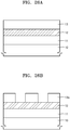
- FIGS. 26A to 26E illustrate a method of forming a pattern using a patterning process according to some example embodiments.
- an etching layer 11 may be formed on a substrate 10.
- a hardmask 12 may be formed on the etching layer 11.
- the hardmask 12 may include an organic hardmask.
- the hardmask 12 may include an inorganic hardmask (e.g., SiON, SiO 2 ).
- a capping layer may be formed on the hardmask.
- a process of providing the hardmask 12 may include at one of spin coating, air spraying, electrospraying, dip coating, spray coating, doctor blade coating, and bar coating.
- inventive concepts are not limited thereto and other deposition processes such as chemical vapor deposition (CVD), plasma-enhanced CVD, and/or sputtering processes may be used to provide the hardmask.
- the substrate 10 is not particularly limited.
- the substrate 10 may be at least one selected from a Si substrate; a glass substrate; a GaN substrate; a silica substrate; a substrate including at least one selected from nickel (Ni), cobalt (Co), iron (Fe), platinum (Pt), palladium (Pd), gold (Au), aluminum (Al), chromium (Cr), copper (Cu), manganese (Mn), molybdenum (Mo), rhodium (Rh), iridium (Ir), tantalum (Ta), titanium (Ti), tungsten (W), uranium (U), vanadium (V), and zirconium (Zr); and a polymer substrate.
- a photoresist layer 13 may be formed on the hardmask 12.
- a photoresist pattern 13a may be formed by exposing the photoresist layer 13 and then developing photoresist layer 13.
- the photoresist layer 13 may be exposed using one of the exposure apparatuses described above in FIGS. 23 to 25 . After the exposing process, heat treatment may be performed on the exposed photoresist layer 13.
- a developing solution e.g., an aqueous solution of tetramethylammonium hydroxide (TMAH)
- TMAH tetramethylammonium hydroxide
- the hardmask 12 may be etched using the photoresist pattern 13a as an etching mask to form a hardmask pattern 12a on the etching layer 11 ( FIG. 26C ).
- the etching process may be performed using a dry etching method using an etching gas.
- the etching gas include at least one selected from CF 4 , CHF 3 , C 2 F 6 , C 4 F 8 , CHF 3 , Cl 2 , and BCl 3 .
- the etching layer 11 may be formed as a plurality of patterns.
- the plurality of patterns may vary, for example, a metal pattern, a semiconductor pattern, and an insulator pattern.
- the plurality of patterns may be various patterns applied to a semiconductor integrated circuit device.
- the etching layer 11 may contain a material that is to be finally patterned.
- the material of the etching layer 11 may be, for example, a metal (e.g., aluminum or copper), a semiconductor (e.g., silicon), or an insulator (e.g., silicon oxide or silicon nitride).
- the etching layer 11 may be formed using various methods (e.g., sputtering, electronic beam deposition, chemical vapor deposition, and physical vapor deposition). For example, the etching layer 11 may be formed using a chemical vapor deposition method.
- the etching layer 11 may be etched using the hardmask pattern 12a as an etching mask to later form an etching layer pattern 11a having a desired fine pattern.
- the hardmask 12 may be omitted and the photoresist pattern 13a may be formed directly on the etching layer 11.
- the etching layer 11 may be used using the photoresist pattern 13a as an etching mask to form the etching layer pattern 11a.
- FIG. 26F illustrates a part of a method of forming a pattern using a patterning process according to some example embodiments.
- a photoresist pattern 13a may be formed on a hard mask 12, etching layer 11, and substrate 10 according to the same operations described above in FIGS. 26A and 26B . Then, a hardmask pattern 12a and etching layer 11 pattern 11a may be formed by etching the hardmask 12 and the etching layer 11 using the photoresist pattern 13a as an etching mask.
Landscapes
- General Physics & Mathematics (AREA)
- Physics & Mathematics (AREA)
- Engineering & Computer Science (AREA)
- Public Health (AREA)
- Environmental & Geological Engineering (AREA)
- Epidemiology (AREA)
- Health & Medical Sciences (AREA)
- Preparing Plates And Mask In Photomechanical Process (AREA)
- Chemical & Material Sciences (AREA)
- Organic Chemistry (AREA)
- Life Sciences & Earth Sciences (AREA)
- General Life Sciences & Earth Sciences (AREA)
- Geology (AREA)
- Inorganic Chemistry (AREA)
- Nanotechnology (AREA)
Abstract
Description
- The present disclosure relates to a pellicle for a photomask, a reticle including the same, and an exposure apparatus for lithography.
- A pellicle for a photomask may be provided in the form of a film on a photomask so as to protect the photomask from external contaminants (for example, dust, resist, or the like) during optical lithography. Such a pellicle may have high transmittance with respect to light used in a lithography process. Such a pellicle may have certain characteristics such as heat dissipation characteristics, strength, uniformity, durability, stability, and the like. As features in semiconductor devices and electronic circuits have become smaller, a wavelength of light used in a lithography process may become shorter. Different pellicle materials are being developed.
- Provided is a pellicle for a photomask, the pellicle having high light transmittance and excellent characteristics in various aspects.
- Provided is a pellicle for a photomask, the pellicle having excellent durability and stability.
- Provided is a pellicle for a photomask, the pellicle having excellent characteristics in terms of thermal conductivity, uniformity, strength, and the like.
- Provided is a pellicle for a photomask, the pellicle having high transmittance and excellent resistance and durability with respect to short-wavelength light such as extreme ultraviolet (EUV) light.
- Provided is a reticle including the pellicle.
- Provided is a lithography apparatus to which the reticle including the pellicle is applied.
- Additional aspects will be set forth in part in the description which follows and, in part, will be apparent from the description, or may be learned by practice of the presented embodiments.
- According to some example embodiments, a pellicle for protecting a photomask includes a pellicle membrane including a carbon-based material having defects and a passivation member covering the defects of the carbon-based material and including an inorganic material.
- In some example embodiments, the carbon-based material may include at least one of graphene, nanocrystalline graphene, reduced graphene oxide (rGO), carbon nanotube (CNT), fullerene, or amorphous carbon.
- In some example embodiments, the defects of the carbon-based material may include at least one of a grain boundary, a vacancy, an sp3 carbon (C) atom, an oxygen (O) atom, or a nitrogen (N) atom.
- In some example embodiments, the carbon-based material may include at least one of graphene, CNT, and fullerene, which may be formed by a growth or synthesis method, and the defects of the carbon-based material may include at least one of a grain boundary or a vacancy.
- In some example embodiments, the carbon-based material may include nanocrystalline graphene. In this case, a D/G intensity ratio in a Raman spectrum of the nanocrystalline graphene may be about 0.5 or more, and a 2D/G intensity ratio in the Raman spectrum of the nanocrystalline graphene may be about 0.05 or more.
- In some example embodiments, an amount of oxygen (O) in the nanocrystalline graphene may be in a range of about 1 at% to about 20 at%.
- In some example embodiments, an amount of hydrogen (H) in the nanocrystalline graphene may be in a range of about 1 at% to about 20 at%.
- In some example embodiments, an amount of nitrogen (N) in the nanocrystalline graphene may be in a range of about 1 at% to about 20 at%.
- In some example embodiments, the passivation member may include a plurality of dot elements.
- In some example embodiments, the plurality of dot elements may selectively cover the defects of the carbon-based material.
- In some example embodiments, the passivation member may have a thin film structure.
- In some example embodiments, the passivation member may be on at least one of an upper surface of the pellicle membrane or a lower surface of the pellicle membrane.
- In some example embodiments, the inorganic material of the passivation member may include at least one of a metal, an oxide, a nitride, a semiconductor, or a metal chalcogenide-based material.
- In some example embodiments, the metal may include at least one of Mo, Ti, or Ru.
- In some example embodiments, the oxide may include MoOx.
- In some example embodiments, the nitride may include at least one of TiN or SiNx.
- In some example embodiments, the semiconductor may include at least one of Ge or ZrSi2.
- In some example embodiments, the metal chalcogenide-based material may include a transition metal chalcogenide.
- In some example embodiments, the passivation member may have a thickness within about 20% of a thickness of the pellicle membrane. The passivation member may have a thickness within about 10% of a thickness of the pellicle membrane.
- In some example embodiments, the passivation member may have a thickness of about 20 nm or less. The passivation member may have a thickness of about 10 nm or less.
- In some example embodiments, the pellicle membrane may have a thickness of about 100 nm or less.
- In some example embodiments, each of the pellicle membrane and the passivation member may have a transmittance of about 80% or more with respect to EUV light.
- In some example embodiments, the pellicle membrane may be spaced apart from the photomask by about 1 mm to about 10 mm.
- In some example embodiments, the pellicle may further include a pellicle frame on an edge portion of the pellicle membrane.
- In some example embodiments, the pellicle may further include a bonding layer between the pellicle membrane and the pellicle frame.
- According to some example embodiments, a reticle includes: a photomask; and the above-described pellicle configured to protect the photomask. The pellicle may be connected to the photomask.
- In some example embodiments, the reticle may be a transmissive reticle.
- In some example embodiments, the reticle may be a reflective reticle.
- In some example embodiments, the reticle may be a reticle for EUV lithography.
- In some example embodiments, an exposure apparatus for lithography includes a light source configured to generate light, and the above-discussed reticle disposed in a traveling path of the light generated by the light source.
- In some example embodiments, the exposure apparatus may further include a first optical member between the reticle and the light source and/or a second optical member between the reticle and a substrate.
- In some example embodiments, the exposure apparatus may be an EUV exposure apparatus.
- According to some example embodiments, a pellicle for protecting a photomask includes a pellicle membrane, a frame, and a passivation member. The pellicle membrane includes a carbon-based material. The carbon-based material has defects. The frame supports the pellicle membrane. The passivation member may be on top of at least one of the frame and the pellicle membrane. The passivation member covers the defects of the carbon-based material. The passivation member includes an inorganic material.
- In some example embodiments, the carbon-based material may include at least one of graphene, nanocrystalline graphene, reduced graphene oxide (rGO), carbon nanotube (CNT), fullerene, or amorphous carbon.
- In some example embodiments, the passivation layer may include a first passivation layer and a second passivation layer. The first passivation layer may be between the frame and the pellicle membrane. The second passivation layer may be on top of the pellicle membrane and the frame.
- In some example embodiments, the inorganic material may include at least one of MoOx, TiN, SiNx, Ge, ZrSi2, or a transition metal chalcogenide.
- In some example embodiments, a reticle may include the photomask and the above-discussed pellicle. The pellicle may be connected to the photomask and configured to protect the photomask.
- In some example embodiments, an exposure apparatus for lithography includes a light source configured to generate light, and the above-discussed reticle disposed in a traveling path of the light generated by the light source.
- These and/or other aspects will become apparent and more readily appreciated from the following description of the embodiments, taken in conjunction with the accompanying drawings in which:
-
FIG. 1 is a cross-sectional view of a pellicle for a photomask, according to some example embodiments; -
FIG. 2 is a cross-sectional view of a pellicle for a photomask, according to some example embodiments; -
FIG. 3 is a cross-sectional view of a pellicle for a photomask, according to some example embodiments; -
FIG. 4 is a cross-sectional view of a pellicle for a photomask, according to a comparative example; -
FIG. 5 shows a result of Raman spectroscopy analysis of a change in properties when a pellicle according to a comparative example is exposed to extreme ultraviolet (EUV) light and EUV light + H2; -
FIG. 6 is a diagram illustrating a case where a fluorine atom is adsorbed onto an internal region other than a graphene edge and then migrates; -
FIG. 7 is a diagram illustrating a case where a fluorine atom is adsorbed onto a graphene edge portion and then undergoes a reaction; -
FIG. 8 is a plan view illustrating an example of a planar form of a graphene layer; -
FIG. 9 is a plan view illustrating a case where a plurality of dot elements covering a grain boundary are formed on the graphene layer ofFIG. 8 ; -
FIG. 10 is a scanning electron microscope (SEM) image showing a case where a plurality of dot elements are formed on a graphene layer along a grain boundary; -
FIG. 11 is a cross-sectional view of a pellicle for a photomask, according to some example embodiments; -
FIG. 12 illustrates a chemical structure of a crystal grain of nanocrystalline graphene applicable to a pellicle membrane according to some example embodiments; -
FIGS. 13A to 13E illustrate chemical structures for describing various possible defects of nanocrystalline graphene applicable to a pellicle membrane according to some example embodiments; -
FIG. 14 is a cross-sectional view for describing a layer structure of nanocrystalline graphene applicable to a pellicle membrane for a photomask, according to some example embodiments. -
FIG. 15 is a cross-sectional view for describing a layer structure of nanocrystalline graphene applicable to a pellicle membrane for a photomask, according to some example embodiments. -
FIG. 16 is a graph showing a result of Raman spectroscopy analysis of nanocrystalline graphene, according to embodiments. -
FIG. 17 is a graph showing a result of X-ray diffraction analysis of nanocrystalline graphenes, according to embodiments. -
FIG. 18 is a cross-sectional view of a pellicle for a photomask, according to some example embodiments; -
FIG. 19 is a cross-sectional view of a pellicle for a photomask, according to some example embodiments; -
FIG. 20 is a cross-sectional view of a reticle including a pellicle for a photomask, according to some example embodiments; -
FIG. 21 is a diagram for describing a problem caused by foreign substances when a lithography process is performed by using a photomask without a pellicle; -
FIG. 22 is a diagram for describing how the influence of foreign substances is removed by a pellicle when a lithography process is performed in a state in which a photomask is protected by the pellicle. -
FIG. 23 is a diagram illustrating an exposure apparatus for lithography, to which a reticle including a pellicle is applied, according to some example embodiments. -
FIG. 24 is a diagram illustrating an exposure apparatus for lithography, to which a reticle including a pellicle is applied, according to some example embodiments. -
FIG. 25 is a diagram illustrating an exposure apparatus for lithography, to which a reticle including a pellicle is applied, according to some example embodiments. -
FIGS. 26A to 26E illustrate a method of forming a pattern using a patterning process according to some example embodiments. -
FIG. 26F illustrates a part of a method of forming a pattern using a patterning process according to some example embodiments. - Reference will now be made in detail to embodiments, examples of which are illustrated in the accompanying drawings, wherein like reference numerals refer to like elements throughout. In this regard, the present embodiments may have different forms and should not be construed as being limited to the descriptions set forth herein. Accordingly, the embodiments are merely described below, by referring to the figures, to explain aspects. As used herein, the term "and/or" includes any and all combinations of one or more of the associated listed items. Expressions such as "at least one of," when preceding a list of elements, modify the entire list of elements and do not modify the individual elements of the list.
- Various example embodiments will now be described more fully with reference to the accompanying drawings in which example embodiments are shown.
- It will be understood that when an element is referred to as being "connected" or "coupled" to another element, it can be directly connected or coupled to the other element or intervening elements may be present. In contrast, when an element is referred to as being "directly connected" or "directly coupled" to another element, there are no intervening elements present. As used herein the term "and/or" includes any and all combinations of one or more of the associated listed items.
- It will be understood that, although the terms "first", "second", etc. may be used herein to describe various elements, components, regions, layers and/or sections, these elements, components, regions, layers and/or sections should not be limited by these terms. These terms are only used to distinguish one element, component, region, layer or section from another element, component, region, layer or section. Thus, a first element, component, region, layer or section discussed below could be termed a second element, component, region, layer or section without departing from the teachings of example embodiments.
- Spatially relative terms, such as "beneath," "below," "lower," "above," "upper" and the like, may be used herein for ease of description to describe one element or feature's relationship to another element(s) or feature(s) as illustrated in the figures. It will be understood that the spatially relative terms are intended to encompass different orientations of the device in use or operation in addition to the orientation depicted in the figures. For example, if the device in the figures is turned over, elements described as "below" or "beneath" other elements or features would then be oriented "above" the other elements or features. Thus, the term "below" can encompass both an orientation of above and below. The device may be otherwise oriented (rotated 90 degrees or at other orientations) and the spatially relative descriptors used herein interpreted accordingly.
- The terminology used herein is for the purpose of describing particular embodiments only and is not intended to be limiting of example embodiments. As used herein, the singular forms "a," "an" and "the" are intended to include the plural forms as well, unless the context clearly indicates otherwise. It will be further understood that the terms "comprises" and/or "comprising," when used in this specification, specify the presence of stated features, integers, steps, operations, elements, and/or components, but do not preclude the presence or addition of one or more other features, integers, steps, operations, elements, components, and/or groups thereof.
- Example embodiments are described herein with reference to cross-sectional illustrations that are schematic illustrations of idealized embodiments (and intermediate structures) of example embodiments. As such, variations from the shapes of the illustrations as a result, for example, of manufacturing techniques and/or tolerances, are to be expected. Thus, example embodiments should not be construed as limited to the particular shapes of regions illustrated herein but are to include deviations in shapes that result, for example, from manufacturing. For example, an implanted region illustrated as a rectangle will, typically, have rounded or curved features and/or a gradient of implant concentration at its edges rather than a binary change from implanted to non-implanted region. Likewise, a buried region formed by implantation may result in some implantation in the region between the buried region and the surface through which the implantation takes place. Thus, the regions illustrated in the figures are schematic in nature and their shapes are not intended to illustrate the actual shape of a region of a device and are not intended to limit the scope of example embodiments.
- Unless otherwise defined, all terms (including technical and scientific terms) used herein have the same meaning as commonly understood by one of ordinary skill in the art to which example embodiments belong. It will be further understood that terms, such as those defined in commonly-used dictionaries, should be interpreted as having a meaning that is consistent with their meaning in the context of the relevant art and will not be interpreted in an idealized or overly formal sense unless expressly so defined herein.
- Hereinafter, pellicles for photomasks, reticles including the same, and exposure apparatuses for lithography, according to embodiments, will be described in detail with reference to the accompanying drawings. Widths and thicknesses of layers or regions in the drawings may be exaggerated for clarity and convenience of explanation. Like reference numerals are assigned to like elements throughout the drawings and the specification.
-
FIG. 1 is a cross-sectional view of a pellicle P10 for a photomask, according to some example embodiments. - Referring to
FIG. 1 , the pellicle P10 may include a pellicle membrane M10. The pellicle membrane M10 may include a carbon-based material having defects. In other words, a constituent material (or a main constituent material) of the pellicle membrane M10 may be a carbon-based material. The carbon-based material may include a two-dimensional (2D) carbon structure or a carbon-based nanomaterial. For example, the carbon-based material may include at least one selected from graphene, nanocrystalline graphene, reduced graphene oxide (rGO), carbon nanotube (CNT), fullerene, and amorphous carbon. The defects of the carbon-based material may include at least one selected from an sp3 carbon (C) atom, an oxygen (O) atom, a nitrogen (N) atom, and a carbon vacancy. Also, the defects may have various forms, for example, a point defect or a line defect such as a grain boundary. - The pellicle P10 may include at least one passivation member, for example, passivation members PS10 and PS20 covering the defects of the carbon-based material. The at least one passivation member may be disposed on at least one of a first surface (e.g., a lower surface) and a second surface (e.g., an upper surface) of the pellicle membrane M10.
FIG. 1 illustrates a case where the first passivation member PS10 is disposed on the lower surface of the pellicle membrane M10, and the second passivation member PS20 is disposed on the upper surface of the pellicle membrane M10. Each of the passivation members PS10 and PS20 may include an inorganic material. The passivation members PS10 and PS20 may serve to suppress or prevent a problem in which characteristics of the pellicle membrane M10 are degraded by light or gas. The light may include extreme ultraviolet (EUV) light, and the gas may include H2. The inorganic material may be a material that is stable in an environment in which EUV energy or H2 gas is used. Therefore, the passivation members PS10 and PS20 including the inorganic material may serve to suppress or prevent the pellicle membrane M10 from being degenerated or degraded by light or gas. In particular, defective regions of the pellicle membrane M10 may be degenerated or degraded relatively easily. Due to the use of the passivation members PS10 and PS20, such a problem may be suppressed or prevented. - The inorganic material of the passivation members PS10 and PS20 may be a material that has high transmittance and excellent resistance and durability with respect to short-wavelength light such as EUV light. Also, the inorganic material may be a material that has relatively excellent strength and uniformity and is prepared by a relatively simple method. For example, the inorganic material may include at least one selected from a metal, an oxide, a nitride, a semiconductor, and a metal chalcogenide-based material. As a specific example, the metal may include at least one selected from Mo, Ti, and Ru. The oxide may be a metal oxide and may include, for example, molybdenum oxide (MoOx). The nitride may be a metal nitride or a non-metal nitride and may include, for example, at least one selected from titanium nitride (TiN) and silicon nitride (SiNx). The semiconductor may include, for example, at least one selected from Ge and zirconium silicide (e.g., ZrSi2). The metal chalcogenide-based material may include a transition metal chalcogenide, and the transition metal chalcogenide may include a transition metal dichalcogenide (TMD). The above-described materials may have high transmittance and excellent resistance and durability with respect to short-wavelength light such as EUV light and may also have excellent strength and uniformity. However, specific materials and kinds of the inorganic material are not limited to those described above and may be changed. For example, the metal may further include Zr or the like, and the semiconductor may further include Si or the like. Various other materials may be applied to the passivation members PS10 and PS20. The passivation members PS10 and PS20 may include the same material or may include at least one different material from each other.
- The pellicle membrane M10 may have a thickness of greater than 0 nm and about 100 nm or less. For example, the pellicle membrane M10 may have a thickness of about 70 nm or less, or about 50 nm or less. The pellicle membrane M10 may have a transmittance of about 80% or more, or about 90% or more, with respect to EUV light. Each of the first and second passivation members PS10 and PS20 may have a thickness less than that of the pellicle membrane M10. For example, each of the first and second passivation members PS10 and PS20 may have a thickness within about 20% or about 10% of a thickness of the pellicle membrane M10. For example, each of the first and second passivation members PS10 and PS20 may have a thickness of about 20 nm or less, about 10 nm or less, or about 5 nm or less. Each of the first and second passivation members PS10 and PS20 may have a transmittance of about 80% or more, or about 90% or more, with respect to EUV light. Each of the first and second passivation members PS10 and PS20 may have a transmittance that is less than or equal to about 100% with respect to EUV light. A case where each of the first and second passivation members PS10 and PS20 has a thickness less than that of the pellicle membrane M10 is advantageous in securing transmittance and thickness uniformity. At least one of the first and second passivation members PS10 and PS20 may be a thin film-type passivation member or an island-type passivation member including a plurality of dot elements.
- The pellicle membrane M10 and the passivation members PS10 and PS20 may be collectively referred to as a membrane layer ML10. That is, the pellicle membrane M10 and the passivation members PS10 and PS20 may constitute the membrane layer ML10. The membrane layer ML10 may be referred to as a "membrane structure". The membrane layer ML10 may have a transmittance of about 80% or more, or about 90% or more, with respect to EUV light.
- The pellicle P10 may further include a pellicle frame F10 so as to support the pellicle membrane M10. Due to the pellicle frame F10, the pellicle membrane M10 may be spaced apart from a photomask (not illustrated) by a certain interval. The pellicle frame F10 may be disposed at an edge portion of the pellicle membrane M10. When viewed from above, the pellicle frame F10 may have a rectangular or circular frame structure or other various shapes. The first passivation member PS10 may be disposed between the pellicle membrane M10 and the pellicle frame F10. In a process of forming the pellicle frame F10, the first passivation member PS10 may serve to protect the pellicle membrane M10.
- The case where the first and second passivation members PS10 and PS20 are disposed on two sides of the pellicle membrane M10 is illustrated in
FIG. 1 , but in some embodiments, one of the passivation members may be disposed at only one side of the pellicle membrane M10. Examples thereof are illustrated inFIGS. 2 and3 . - As illustrated in
FIG. 2 , the passivation member PS10 may be disposed on one surface of the pellicle membrane M10, for example, the lower surface of the pellicle membrane M10. Also, as illustrated inFIG. 3 , the passivation member PS20 may be disposed on another surface of the pellicle membrane M10, for example, the upper surface of the pellicle membrane M10. Even though the passivation member PS10 or PS20 is disposed on only one side of the pellicle membrane M10, the passivation member PS10 or P20 may protect the pellicle membrane M10. - In
FIG. 2 , the pellicle membrane M10 and the passivation member PS10 may constitute a membrane layer ML11, and the membrane layer ML11 and the pellicle frame F10 may constitute a pellicle P11 for a photomask. Similarly, inFIG. 3 , the pellicle membrane M10 and the passivation member PS20 may constitute a membrane layer ML12, and the membrane layer ML12 and the pellicle frame F10 may constitute a pellicle P12 for a photomask. -
FIG. 4 is a cross-sectional view of a pellicle P1 for a photomask, according to a comparative example. - Referring to
FIG. 4 , the pellicle P1 according to the comparative example may include a pellicle membrane GL1 including a graphene layer. That is, the pellicle membrane GL1 may be a graphene layer. The pellicle membrane GL1 may not include the passivation members PS10 and PS20 described above with reference toFIGS. 1 to 3 . A pellicle frame F1 supports the pellicle membrane GL1. - When the pellicle P1 of
FIG. 4 according to the comparative example is used, the pellicle P1 may be easily degenerated and degraded by EUV light or EUV light + H2. This will be described below with reference toFIG. 5 . -
FIG. 5 shows a result of Raman spectroscopy analysis of a change in properties when the pellicle P1 according to the comparative example was exposed to EUV light and EUV light + H2. For example,FIG. 5 shows Raman spectroscopy plots of a case where the pellicle P1 was in a pristine state, a case where the pellicle P1 was exposed to EUV light, and a case where the pellicle P1 was exposed to EUV light + H2. InFIG. 5 , D peak is a peak appearing at about 1,340 cm-1 to about 1,350 cm-1, G peak is a peak appearing at about 1,580 cm-1, and 2D peak is a peak appearing at about 2,700 cm-1. - Referring to
FIG. 5 , it can be seen that the heights and ratios of peaks were changed in the case of exposure to EUV light and EUV light + H2, as compared with the pristine state. In particular, it can be seen that the D peak changed greatly. In the case of exposure to EUV light, the height of the D peak was increased, and in the case of exposure to EUV light + H2, the height of the D peak was more greatly increased. This means that characteristics of the pellicle membrane (GL1 inFIG. 4 ) (that is, the graphene layer) were degenerated and degraded by EUV light and EUV light + H2. As the pellicle membrane (graphene layer) is exposed to EUV light and EUV light + H2, the pellicle membrane (graphene layer) may be gradually etched and characteristics of the pellicle membrane (graphene layer), such as transmittance, may be changed. Such a problem may be caused by a defective region of the pellicle membrane (graphene layer). -
FIG. 6 is a diagram illustrating a case where a fluorine (F) atom is adsorbed onto an internal region other than a graphene edge and then migrates. - Referring to
FIG. 6 , the fluorine (F) atom may be adsorbed onto the internal region other than the graphene edge and may not migrate easily. Energy required for the migration of the fluorine (F) atom may be about 5.5 kcal/mol or more. Therefore, the internal region of graphene may have very low reactivity. In other words, the internal region of graphene may have relatively excellent stability. -
FIG. 7 is a diagram illustrating a case where a fluorine atom is adsorbed onto a graphene edge portion and then undergoes a reaction. - Referring to
FIG. 7 , the fluorine (F) atom may be well adsorbed onto the graphene edge portion and undergo a reaction. Energy required to change from an (a) state to a (b) state may be about -51.7 kcal/mol. The (a) state is a state in which no fluorine (F) atom is adsorbed onto a graphene edge, and the (b) state is a state in which one fluorine (F) atom is adsorbed onto a graphene edge. That the energy required to change from the (a) state to the (b) state is a negative (-) value means that such a reaction can easily occur. Energies required to change from the (b) state to a (c) state, from the (c) state to a (d) state, from the (d) state to an (e) state, and from the (e) state to an (f) state may all have a negative value. In particular, breakage of C-C bonds occurs in the process of changing from the (c) state to the (d) state. Energy required at this time may be about -46.4 kcal/mol, and this may be an exothermic reaction. As such, the graphene edge region, e.g., the defective region, may have relatively high reactivity with an external atom, and degeneration and degradation may easily progress therein. -
FIGS. 6 and7 illustrate an example in which the fluorine (F) atom is adsorbed and undergoes a reaction, and a type of an atom that is adsorbed and undergoes a reaction may be variously changed. Also, the positive (+) or negative (-) energies described with reference toFIGS. 6 and7 are based on simulation and may be different from actual energies. -
FIG. 8 is a plan view illustrating an example of a planar form of a graphene layer. - Referring to
FIG. 8 , the graphene layer may have a plurality of crystal grains and a grain boundary therebetween. The grain boundary may be a type of a graphene edge. The graphene layer may not have a monocrystalline structure as a whole and may include a plurality of crystal grains and a grain boundary therebetween. -
FIG. 9 is a plan view illustrating an example in which a plurality of dot elements covering the grain boundary are formed on the graphene layer ofFIG. 8 . - Referring to
FIG. 9 , the dot elements covering the grain boundary may be formed on the graphene layer. The dot elements may include an inorganic material and may be formed along the grain boundary. The dot elements may be an example of the passivation member PS10 or PS20 described above with reference toFIG. 1 . The dot elements may selectively cover the defective region of the graphene layer, that is, the grain boundary. In forming the dot elements, since the internal region of graphene of the graphene layer has hydrophobicity and low reactivity and the grain boundary region has relatively high reactivity, the dot elements may be formed along the grain boundary region. These dot elements may serve to protect the graphene layer from light and gas used in a lithography process. Each of the dot elements may have a size (diameter) of tens of nm or less, but in some embodiments, may have a size (diameter) of about 100 nm or more. -
FIG. 10 is a scanning electron microscope (SEM) image showing a case where a plurality of dot elements are formed on a graphene layer along a grain boundary. - Referring to
FIG. 10 , a plurality of inorganic dots may be formed along a graphene edge, that is, a grain boundary. - According to some example embodiments, the passivation member may not be a multi-dot type but a thin film type. One example thereof is illustrated in
FIG. 11 . -
FIG. 11 is a cross-sectional view for describing a pellicle for a photomask, according to some example embodiments. Referring toFIG. 11 , the pellicle may include thin film-type passivation layers PS11 and PS22 on a graphene layer GL10. The passivation layers PS11 and PS22 may be disposed on one or two surfaces of the graphene layer GL10.FIG. 11 illustrates a case where first and second passivation layers PS11 and PS22 are disposed on two surfaces of the graphene layer GL10. The passivation layers PS11 and PS22 may have a continuous layer shape. The thin film-type passivation layers PS11 and PS22 may be formed according to a process or condition for forming the passivation layers PS11 and PS22. Each of the passivation layers PS11 and PS22 may have a thickness less than that of the graphene layer GL10. Each of the passivation layers PS11 and PS22 may have a thickness within about 20% or about 10% of a thickness of the graphene layer GL10. For example, each of the passivation layers PS11 and PS22 may have a thickness of about 20 nm or less, about 10 nm or less, or about 5 nm or less. The graphene layer GL10 may be an example of the pellicle membrane. - A carbon-based material formed by a growth or synthesis method may include defects. For example, graphene, CNT, or fullerene formed by the growth or synthesis method may have defects such as a grain boundary or a vacancy. The vacancy may be a carbon vacancy. Also, the carbon-based material formed by the growth or synthesis method may include, as the defects, at least one selected from an oxygen (O) atom, a nitrogen (N) atom, and a hydrogen (H) atom. In the case of synthesizing the CNT, acid treatment may be performed in a refining process after synthesis, and defects may be generated by the acid treatment. Since such defects of the carbon-based material have good reactivity, the protection provided by the passivation member may be advantageous in limiting and/or preventing degeneration and degradation. The passivation members PS11 and PS22 may include the same material or may include at least one different material from each other.
- A method of forming the dot-type passivation members (that is, inorganic dots) of
FIGS. 9 and10 and the thin film-type passivation members (passivation layers) ofFIG. 11 will be described below. The passivation members according to some example embodiments may be formed by using a deposition process or a solution process. The deposition process may be chemical vapor deposition (CVD), atomic layer deposition (ALD), or physical vapor deposition (PVD). The solution process may be performed by coating a solution including a source material on a membrane (for example, a graphene layer) and performing a drying and/or annealing process thereon. The coating method may be, for example, spin coating. Dot-type passivation members or thin film-type passivation members may be formed according to a type or a specific condition of the deposition process or the solution process. For example, since the internal region of graphene of the membrane (e.g., the graphene layer) has hydrophobicity and low reactivity and the grain boundary region has relatively high reactivity, the dot-type passivation member may be formed along the grain boundary region. Also, dot-type passivation members or thin film-type passivation members may be formed according to a concentration of the source material included in the solution used in the solution process. However, the above-described method of forming the passivation members is merely an example and may be changed. - The pellicle membranes M10 of
FIGS. 1 to 3 may include, for example, nanocrystalline graphene. Hereinafter, nanocrystalline graphene, which may be included in the pellicle membrane M10, will be described in detail with reference toFIGS. 12 and13A to 13E . -
FIG. 12 illustrates a chemical structure of a crystal grain of nanocrystalline graphene applicable to a pellicle membrane M10 ofFIGS. 1 to 3 . In the case ofFIG. 12 , it is assumed that the crystal grain does not include any defects, but an actual crystal grain may include defect(s). - Referring to
FIG. 12 , the crystal grain may include a "2D carbon structure" having an aromatic ring structure. Carbon atoms may form an aromatic ring structure, and such ring structures (annular structures) may be two-dimensionally arranged. A size of the crystal grain may be nanoscale. A size (length/diameter) of the crystal grain may be several hundreds of nm or less, for example, about 100 nm or less. The size, shape, and structure of the crystal grain illustrated inFIG. 12 are merely examples and may be variously changed. Possible defects of the crystal grain will be described with reference toFIGS. 13A to 13E . -
FIGS. 13A to 13E illustrate chemical structures for describing various possible defects of the nanocrystalline graphene applicable to the pellicle membrane M10 ofFIGS. 1 to 3 . In other words,FIGS. 13A to 13E illustrate possible defects of the crystal grain ofFIG. 12 . -
FIG. 13A illustrates a case where some carbon atoms forming an aromatic ring structure become sp3 carbons when double bonds thereof are broken, and hydroxy groups (OH) are bonded to the sp3 carbons. Carbon atoms maintaining double bonds in the aromatic ring structure may be referred to as sp2 carbons. Since all carbon atoms constituting general graphene may be sp2 carbons, the sp3 carbons may be regarded as defects of graphene. Also, a functional group (or a substituent) such as the hydroxy group (OH) bonded to the sp3 carbon may be regarded as defects. -
FIG. 13B illustrates a case where some carbon atoms forming an aromatic ring structure become sp3 carbons when double bonds thereof are broken, and an oxygen (O) atom is bonded to the sp3 carbons. The oxygen (O) atom may be bonded to two adjacent sp3 carbons. Such an oxygen (O) atom may be referred to as an epoxy group. -
FIG. 13C illustrates a case where some carbon atoms forming an aromatic ring structure become sp3 carbons when double bonds thereof are broken, and hydrogen (H) atoms are bonded to the sp3 carbons. In some cases, a hydrogen (H) atom may be bonded to one of the two adjacent sp3 carbons, and a hydroxy group (OH) may be bonded to the other. -
FIG. 13D illustrates a case where some carbon atoms forming an aromatic ring structure become sp3 carbons when double bonds thereof are broken, and a carboxyl group (COOH) is bonded to the sp3 carbon. Since the carboxyl group (COOH) may include a carbonyl group (C=O), it can also be said that the carbonyl group (C=O) is bonded to the sp3 carbon. -
FIG. 13E illustrates a case where a carbon vacancy is generated in a 2D carbon structure having an aromatic ring structure. It can be said thatFIGS. 13A to 13D illustrate a case where a functional group (or a substituent) or other atoms (atoms except for carbon) are bonded to the sp3 carbon, andFIG. 13E illustrates a case where a carbon vacancy is generated without a functional group (or a substituent). - Various types of defects described with reference to
FIGS. 13A to 13E may be applied to the crystal grain illustrated inFIG. 12 . In other words, various types of defects may be included in the nanocrystalline graphene constituting the pellicle membrane M10 ofFIGS. 1 to 3 . However, such defects described with reference toFIGS. 13A to 13E are merely examples and other types of defects may also be present. For example, the defects may include a nitrogen (N) atom. In this case, the nitrogen atom may be bonded to the sp3 carbon in the form of NH2. In other words, inFIG. 13A , NH2 instead of OH may be bonded to the sp3 carbon. At least two of the nitrogen atom and the various types of defects described with reference toFIGS. 13A to 13E may be included in one nanocrystalline graphene or one crystal grain. Also, defects other than the above-described defects may be present. - Defects of the nanocrystalline graphene may include at least one selected from an sp3 carbon atom, an oxygen atom, a nitrogen atom, and a carbon vacancy. Herein, the oxygen atom may be the oxygen atom included in OH of
FIG. 13A , the oxygen atom ofFIG. 13B , or the oxygen atom included in COOH ofFIG. 13D , or may also be present in various forms. The nitrogen atom may be included in the form of, for example, NH2, or may also be included in various forms. Also, the hydrogen (H) atoms included OH ofFIG. 13A , H ofFIG. 13C , and COOH ofFIG. 13D may be regarded as defects. An amount (content) of hydrogen (H) in the nanocrystalline graphene may be larger than that in general graphene (for example, monocrystalline graphene). In a case where sheet-type monocrystalline graphene has defects at an edge portion thereof (however, the graphene may not have defects at the edge portion thereof), a very small amount of hydrogen (H) may be present only at the edge portion. An amount of hydrogen (H) in the nanocrystalline graphene may be larger than that in the monocrystalline graphene. However, an amount of hydrogen (H) in the nanocrystalline graphene may be smaller than that in an amorphous carbon layer (ACL). An amount of hydrogen (H) in the ACL may be about 23.6 at%, and an amount of hydrogen (H) in the nanocrystalline graphene may be smaller than about 23.6 at%. - An amount (content) of oxygen (O) in the nanocrystalline graphene described with reference to
FIGS. 1 to 13E may be in a range of about 12 at% to about 40 at%. For example, an amount of oxygen (O) in the nanocrystalline graphene may be in a range of about 1 at% to about 20 at%, or about 1 at% to about 10 at%. An amount (content) of hydrogen (H) in the nanocrystalline graphene may be in a range of about 1 at% to about 25 at%. For example, an amount of hydrogen (H) in the nanocrystalline graphene may be in a range of about 1 at% to about 20 at%. In a case where the nanocrystalline graphene includes nitrogen (N), an amount (content) of nitrogen (N) in the nanocrystalline graphene may be in a range of about 1 at% to about 30 at%. For example, an amount of nitrogen (N) in the nanocrystalline graphene may be in a range of about 1 at% to about 20 at%. However, the nanocrystalline graphene may contain about 1 at% or less of nitrogen (N) or may not contain nitrogen (N). - On the other hand, in a Raman spectrum of the nanocrystalline graphene, an intensity ratio of D peak to G peak, e.g., a D/G intensity ratio, may be about 0.5 or more. The G peak is a peak appearing at about 1,580 cm-1. The G peak may be caused in a vibration mode corresponding to stretching of a carbon-carbon bond and provide information capable of determining the inclusion or non-inclusion of an aromatic ring structure. The D peak is a peak appearing in a range of about 1,340 cm-1 to about 1,350 cm-1. The D peak may be generated by defects such as an sp3 carbon and a carbon vacancy. In the Raman spectrum of the nanocrystalline graphene, the D/G intensity ratio may be about 0.5 or more. The D/G intensity ratio may be about 1 or more. The D/G intensity ratio may be about 2 or less.
- In the Raman spectrum of the nanocrystalline graphene, an intensity ratio of 2D peak to G peak, e.g., a 2D/G intensity ratio, may be about 0.05 or more. The 2D peak is a peak appearing at about 2,700 cm-1 and provides information capable of determining an amount of an aromatic ring structure. The 2D/G intensity ratio may be about 0.05 or more. For example, the 2D/G intensity ratio may be about 0.1 or more. The 2D/G intensity ratio may be about 1 or less. However, in some cases, the 2D/G intensity ratio may be greater than about 1. Conditions related to the Raman spectrum of the nanocrystalline graphene according to the embodiment will be described below with reference to
FIG. 16 and the like. -
FIG. 14 is a cross-sectional view for describing a layer structure of nanocrystalline graphene NG11 applicable to a pellicle membrane for a photomask, according to some example embodiments. - Referring to
FIG. 14 , the nanocrystalline graphene NG11 applicable to the pellicle may include a plurality of crystal grains G11. A size (length/diameter) of each of the crystal grains G11 may be several hundreds of nm or less, for example, about 100 nm or less. The crystal grains G11 may be roughly arranged (aligned) in a direction parallel to the nanocrystalline graphene NG11. The nanocrystalline graphene NG11 may have an irregular lattice structure in a vertical direction, that is, a C-axis direction. In other words, the crystal grains G11 may not have a regular or ordered lattice structure, such as graphite, in the C-axis direction. - However, the crystal grains G11 may have a regular (or relatively regular) lattice structure in the C-axis direction in some regions of the nanocrystalline graphene NG11. Even in this case, the crystal grains G11 may have an irregular lattice structure in the C-axis direction in another region of the nanocrystalline graphene NG11. Therefore, when taking into account the entire regions, the nanocrystalline graphene NG11 may be said to have an irregular lattice structure in the C-axis direction.
- An interlayer spacing, e.g., a d-spacing of the nanocrystalline graphene NG11 may be greater than a d-spacing of graphite. In other words, the d-spacing of the nanocrystalline graphene NG11 may be greater than about 3.35 Å. For example, the d-spacing of the nanocrystalline graphene NG11 may be about 3.4 Å or more. The d-spacing may be obtained by X-ray diffraction analysis. The nanocrystalline graphene NG11 may have an increased d-spacing since the nanocrystalline graphene NG11 has a nanocrystalline structure and includes defects.
-
FIG. 15 is a cross-sectional view for describing a layer structure of nanocrystalline graphene NG12 applicable to a pellicle membrane for a photomask, according to some example embodiments. - Referring to
FIG. 15 , the nanocrystalline graphene NG12 applicable to the pellicle may include a plurality of crystal grains G12. A size (length/diameter) of each of the crystal grains G12 may be several hundreds of nm or less, for example, about 100 nm or less. The crystal grains G12 may be arranged in a random direction or a relatively random direction. Therefore, the nanocrystalline graphene NG12 may have an irregular lattice structure in a C-axis direction. However, the crystal grains G12 may have a regular (or relatively regular) lattice structure in the C-axis direction in some regions (fine regions) of the nanocrystalline graphene NG12. A d-spacing of the nanocrystalline graphene NG12, as obtained through X-ray diffraction analysis, may be greater than about 3.35 Å. For example, the d-spacing of the nanocrystalline graphene NG12 may be about 3.4 Å or more. - A density of the nanocrystalline graphenes NG11 and NG12 may be less than a density of graphite. For example, the density of the nanocrystalline graphenes NG11 and NG12 may be less than about 2.2 g/cm3. The density of the nanocrystalline graphenes NG11 and NG12 may be less than about 2.15 g/cm3. In some cases, the density of the nanocrystalline graphenes NG11 and NG12 may be less than about 2.0 g/cm3. The density of the nanocrystalline graphenes NG11 and NG12 may be greater than a density of an amorphous carbon layer (ACL). In this regard, the density of the nanocrystalline graphenes NG11 and NG12 may be greater than about 1.5 g/cm3. Thus, the density of the nanocrystalline graphenes NG11 and NG12 may be greater than about 1.5 g/cm3 and less than about 2.2 g/cm3.
- The layer structures of the nanocrystalline graphenes NG11 and NG12 described with reference to
FIGS. 14 and 15 are merely examples and may be variously changed. The structures ofFIGS. 14 and 15 may be mixed. Also, one of a lower layer region and an upper layer region of one nanocrystalline graphene may have the structure ofFIG. 14 , and the other may have the structure ofFIG. 15 . Other various structures may be applied to the nanocrystalline graphenes NG11 and NG12. - The nanocrystalline graphenes NG11 and NG12 may be formed by using various methods. For example, the nanocrystalline graphenes NG11 and NG12 may be formed by using a deposition process, such as chemical vapor deposition (CVD) or a solution process using a graphene-containing solution. Next, the method of forming the nanocrystalline graphenes NG11 and NG12 by using the deposition process and the solution process will be described in detail.
- Nanocrystalline graphene may be formed by using the deposition process such as CVD. The CVD may be thermal CVD or plasma CVD. Examples of the plasma CVD may include inductively coupled plasma CVD (ICP-CVD) and plasma enhanced CVD (PE-CVD). The CVD may use a gas source or a solid source (for example, a source of carbon). The solid source may include polymer, organic monomer, or the like. The nanocrystalline graphene may be formed by adjusting a type (material) of a substrate and a process temperature (deposition temperature) in the deposition process. Also, in forming the nanocrystalline graphene, an amount or type of defects included in the nanocrystalline graphene may be adjusted by additionally using defect-causing materials. Unlike amorphous carbon, the nanocrystalline graphene has crystallinity. However, the crystallinity of the nanocrystalline graphene NG1 may be lower than that of graphite or monocrystalline graphene. Also, various characteristics may be exhibited by defects included in the nanocrystalline graphene.
- Next, the method of forming the nanocrystalline graphene by using a solution process will be described in detail. A graphene-containing solution may be prepared by dissolving graphene particles, each having a size of several tens of nm or less, in a certain solvent. A film may be formed by coating the solution on a certain substrate (underlayer). Then, nanocrystalline graphene may be formed from the film by performing annealing or heat treatment on the film. The graphene particles may be graphene quantum dots (GQDs) or graphene nanoplates. Also, graphene oxide particles may be used instead of the graphene particles or together with the graphene particles. The solvent may include at least one selected from N-methylpyrrolidone (NMP), dimethylformamide (DMF), and NH4OH, but inventive concepts are not limited thereto. The process of coating the solvent on the substrate (underlayer) may be performed by using various coating methods or film casting methods. The annealing or heat treatment may be performed on the film coated on the substrate (underlayer) at a temperature lower than about 2,000°C. For example, the annealing or heat treatment may be performed at a temperature of about 1,200°C or lower, but may be performed at a temperature higher than about 1,200°C. The nanocrystalline graphene may be formed in the above-described manner. Crystallinity or defects of the nanocrystalline graphene may be adjusted by controlling the temperature or atmosphere of the annealing or heat treatment. In some cases, defect-causing materials may be additionally used.
- The nanocrystalline graphene formed in the above-described manner may have excellent uniformity. The nanocrystalline graphene may have excellent thickness uniformity and surface uniformity. For example, the surface roughness of the nanocrystalline graphene may be less than about 10 nm. The surface roughness of the nanocrystalline graphene may be about 6 nm or less, or about 3 nm or less. The nanocrystalline graphene may show uniform light transmittance as a whole. Therefore, when the nanocrystalline graphene is used in a pellicle membrane for lithography, uniformity and precision of the lithography process may be easily secured.
- Also, the nanocrystalline graphene may have high transmittance with respect to a certain wavelength range of light. For example, the nanocrystalline graphene may have a transmittance of about 80% or more, or about 90% or more, with respect to extreme ultraviolet (EUV) light. The nanocrystalline graphene may have a transmittance of about 80% or more, or about 90% or more, with respect to EUV light in a thickness range of about 5 nm to about 100 nm. The nanocrystalline graphene may be usefully applied to an EUV lithography apparatus.
- Also, the nanocrystalline graphene may have high thermal conductivity, excellent heat dissipation characteristics, excellent EUV resistance, and excellent mechanical strength (tensile strength). For example, the nanocrystalline graphene may have an in-plane thermal conductivity of several thousands of W/m·k, a Young's modulus of several hundreds of GPa or more, and a tensile strength of several tens of GPa or more, or about 100 GPa or more. Compared with poly-Si that has an in-plane thermal conductivity of about 15 W/m·k to about 35 W/m·k, a Young's modulus of about 170 GPa, and a tensile strength of about 1.5 GPa, the nanocrystalline graphene may have excellent characteristics as a material of the pellicle membrane in various aspects. Also, the nanocrystalline graphene may have excellent durability and stability.
- When the nanocrystalline graphene is applied to the pellicle membrane M10 of
FIGS. 1 to 3 , the nanocrystalline graphene may have a thickness of about 100 nm or less. In other words, the pellicle membrane M10 including the nanocrystalline graphene may have a thickness of about 100 nm or less. For example, the nanocrystalline graphene may have a thickness of about 50 nm or less. The nanocrystalline graphene may have a transmittance of about 80% or more, or about 90% or more, with respect to EUV light. -
FIG. 16 is a graph showing a result of Raman spectroscopy analysis of nanocrystalline graphene, according to embodiments. InFIG. 16 , nanocrystalline graphene ncG1 and nanocrystalline graphene ncG2 were formed by a deposition process. The nanocrystalline graphene ncG1 differs from the nanocrystalline graphene ncG2 in terms of a process temperature. The nanocrystalline graphene ncG1 was formed at a process temperature of 560°C, and the nanocrystalline graphene ncG2 was formed at a process temperature of 590°C. - Referring to
FIG. 16 , it can be seen that G peak, D peak, and 2D peak appear in a Raman spectrum. A D/G intensity ratio may be about 0.5 or more. The D/G intensity ratio may be about 1 or more. The D/G intensity ratio may be about 2 or less. A 2D/G intensity ratio may be about 0.05 or more. For example, the 2D/G intensity ratio may be about 0.1 or more. The 2D/G intensity ratio may be about 1 or less. -
FIG. 17 is a graph showing a result of X-ray diffraction analysis of nanocrystalline graphenes, according to embodiments. In the graph ofFIG. 17 , 2θ or the like at which the peak appears may be obtained. By using this information, an interlayer spacing (e.g., d-spacing (d002)) of the nanocrystalline graphene may be calculated. A d-spacing of the nanocrystalline graphene may be greater than about 3.35 Å. For example, the d-spacing of the nanocrystalline graphene may be 3.4 Å or more. - The nanocrystalline graphene, which may be included in the pellicle membrane (M10 in
FIGS. 1 to 3 ), has been illustrated and described inFIGS. 12 to 17 , but the pellicle membrane M10 may include graphene other than the nanocrystalline graphene, or may include rGO, CNT, fullerene, amorphous carbon, or the like. The graphene other than the nanocrystalline graphene may be monocrystalline graphene or polycrystalline graphene. The monocrystalline graphene or the polycrystalline graphene may have thermal conductivity (in-plane thermal conductivity) of several thousands of W/m·k, a Young's modulus of several hundreds of GPa or more, and a tensile strength of several tens of GPa or more, and may have a transmittance of about 80% or more, or about 90% or more, with respect to EUV light at a thickness of several tens of nm. Also, the monocrystalline graphene or the polycrystalline graphene may have excellent durability and stability. In this regard, the monocrystalline graphene or the polycrystalline graphene may also have excellent characteristics as a material of the pellicle membrane, in terms of various aspects. -
FIG. 18 is a cross-sectional view of a pellicle P15 for a photomask, according to some example embodiments. - Referring to
FIG. 18 , the pellicle P15 may include a pellicle membrane M15. The pellicle membrane M15 may include a carbon-based material. The carbon-based material may include a 2D carbon structure or a carbon-based nanomaterial. For example, the carbon-based material may include at least one selected from graphene, nanocrystalline graphene, rGO, CNT, fullerene, and amorphous carbon. - The pellicle P15 may include at least one of passivation members PS15 and PS25 on at least one surface of the pellicle membrane M15.
FIG. 18 illustrates a case where the first passivation member PS15 is disposed on a lower surface of the pellicle membrane M15, and the second passivation member PS25 is disposed on an upper surface of the pellicle membrane M15. Each of the passivation members PS15 and PS25 may include an inorganic material. For example, the inorganic material may include at least one selected from a metal, an oxide, a nitride, a semiconductor, and a metal chalcogenide-based material. The first and second passivation members PS15 and PS25 may correspond to the first and second passivation members PS10 and PS20 ofFIG. 1 , respectively. - The pellicle P15 according to the present embodiment may further include at least one of a first protective layer PL15 disposed on a surface of the first passivation member PS15 and a second protective layer PL25 disposed on a surface of the second passivation member PS25. The first passivation member PS15 may be disposed between the first protective layer PL15 and the pellicle membrane M15. The second passivation member PS25 may be disposed between the second protective layer PL25 and the pellicle membrane M15. The first protective layer PL15 and the first passivation member PS15 may include different materials or similar or identical materials. Similarly, the second protective layer PL25 and the second passivation member PS25 may include different materials or similar or identical materials. At least one of the first and second protective layers PL15 and PL25 may include an inorganic material, and the inorganic material may be identical or similar to the inorganic material of the passivation member PS15 or PS25. Also, at least one of the first and second protective layers PL15 and PL25 may include at least one selected from a metal chalcogenide-based material, a silicon derivative, and a metal oxide. The metal chalcogenide-based material may include, for example, a transition metal dichalcogenide (TMD). As a specific example, the metal chalcogenide-based material may include one metal element selected from the group consisting of Mo, W, Nb, V, Ta, Ti, Zr, Hf, Tc, Re, Cu, Ga, In, Sn, Ge, and Pb, and one chalcogen element selected from the group consisting of S, Se, and Te. When the first and second protective layers PL15 and PL25 include the metal chalcogenide-based material, excellent uniformity and transmittance may be secured. In particular, the TMD may have a surface roughness of several nanometers or less and may have a high transmittance of about 90% or more with respect to EUV light. Also, the first and second protective layers PL15 and PL25 may include other materials except for the metal chalcogenide-based material. For example, the first and second protective layers PL15 and PL25 may include a silicon derivative or a metal oxide. The silicon derivative may include, for example, at least one selected from the group consisting of Si, SiOx, and SixNy. SiOx may be SiO2, and SixNy may be Si3N4. The metal oxide may include, for example, at least one metal element selected from the group consisting of Hf, Al, Mg, Zr, Cu, Ni, Zn, and Ti, and an oxygen (O) atom. Also, the first and second protective layers PL15 and PL25 may include a metal, a metallic compound, or a 2D material. The pellicle membrane M15, the first and second passivation members PS15 and PS25, and the first and second protective layers PL15 and PL25 may constitute a membrane layer ML15. The pellicle P15 may not include at least one of the first and second protective layers PL15 and PL25.
-
FIG. 19 is a cross-sectional view of a pellicle P17 for a photomask, according to some example embodiments. - Referring to
FIG. 19 , the pellicle P17 may further include a bonding layer B10 between a membrane layer ML10 and a frame F10. Although the membrane layer ML10 is simply illustrated for convenience, the membrane layer ML10 may have substantially the same configuration as those of the membrane layers ML10 to ML12 and ML15 described above with reference toFIGS. 1 to 3 and18 , or may have a configuration modified therefrom. The bonding layer B10 may more tightly bond the membrane layer ML10 to the frame F10. Various materials used as adhesive or bonding materials in the fields of general semiconductor devices and electronic circuits may be applied as the material of the bonding layer B10.FIG. 19 illustrates a case where the bonding layer B10 is provided in the structure ofFIG. 1 , but the bonding layer B10 may also be provided in the structures ofFIGS. 2 ,3 , and18 . -
FIG. 20 is a cross-sectional view of a reticle R100 including a pellicle P100 for a photomask PM10, according to some example embodiments. - Referring to
FIG. 20 , the reticle R100 may include the photomask PM10, and the pellicle P100 configured to protect the photomask PM10. The photomask PM10 may include a mask substrate MS10, and a mask pattern MP10 on the mask substrate MS10. A shape, size, and interval of the mask pattern MP10 are merely examples, and may be variously changed. - The pellicle P100 may include a membrane layer M100 spaced apart from the mask pattern MP10. Although the membrane layer M100 is simply illustrated for convenience, the membrane layer M100 may have substantially the same configuration as those of the membrane layers ML10 to ML12 and ML15 described above with reference to
FIGS. 1 to 3 and18 , or may have a configuration modified therefrom. The membrane layer M100 may have a first horizontal length of several tens of mm to several hundreds of mm and a second horizontal length (width) of several tens of mm to several hundreds of mm. The membrane layer M100 may have a thickness of about 150 nm or less, or about 100 nm or less. For example, the membrane layer M100 may have a thickness of about 70 nm or less, or about 50 nm or less. - The pellicle P100 may further include a frame F100 disposed at an edge portion of the mask pattern MP10 to support the membrane layer M100. Due to the frame F100, the photomask PM10 and the membrane layer M100 may be spaced apart from each other by a certain internal d. In other words, due to the frame F100, the mask pattern MP10 of the photomask PM10 and the membrane layer M100 may be spaced apart from each other by a certain internal d. The interval d may be about 15 mm or less. For example, the interval d may be about 1 mm to about 10 mm. Although not illustrated, a bonding layer may be further provided between the membrane layer M100 and the frame F100. Also, a bonding layer may be further provided between the frame F100 and the photomask PM10.
- The pellicle P100 may protect the photomask PM10 from external contaminants (for example, dust, resist, or the like). When the pellicle P100 is absent, foreign substances may be attached to the photomask PM10, causing various problems in the lithography process. Details thereof will be described below with reference to
FIG. 21 . -
FIG. 21 is a diagram for describing a problem caused by foreign substances D1 when a lithography process is performed by using a photomask PM11 without a pellicle. - Referring to
FIG. 21 , when the lithography process is performed by using the photomask PM11 without a pellicle, the foreign substances D1 may be directly attached to the photomask PM11. The photomask PM11 may include a mask substrate MS11 and a mask pattern MP11, and the foreign substances D1 may be directly attached to the mask pattern MP11. - Light L1 generated by a light source (not illustrated) may pass through the photomask PM11 and a lens unit LU10, and a resist layer RL10 of a substrate SUB10 may be exposed to the light L1. Through such an exposure process, a pattern corresponding to the mask pattern MP11 may be transferred onto the resist layer RL10. However, when the foreign substances D1 are directly attached to the mask pattern MP11 or a region of the mask substrate MS11 exposed by the mask pattern MP11, the foreign substances D1 may have a direct influence on patterning of the resist layer RL10. That is, light passing through the foreign substances D1 may be focused on the resist layer RL10. Due to this, an unintended region of the resist layer RL10 may be exposed. Consequently, patterns having a desired (intended) shape may not be realized on the resist layer RL10. In particular, as a width (line width) of a pattern to be formed becomes narrower, the influence of the foreign substances D1 may further increase.
-
FIG. 22 is a diagram for describing how the influence of foreign substances D1 is removed by a pellicle P110 when a lithography process is performed in a state in which a photomask PM11 is protected by the pellicle P110. For example,FIG. 22 illustrates a case where the lithography process is performed in a state in which the photomask PM11 illustrated inFIG. 21 is protected by the pellicle P110. The pellicle P110 may include a membrane layer M110 and a frame F110 and may correspond to the pellicle P100 ofFIG. 20 . - Referring to
FIG. 22 , when the pellicle P110 protects the photomask PM11, the foreign substances D1 may be attached to the outside of the pellicle P110. For example, the foreign substances D1 may be attached to the outer surface of the membrane layer M110. Thus, the foreign substances D1 may be spaced apart from the mask pattern MP11 by a certain interval. In this case, the foreign substances D1 may have no or almost no influence on patterning of the resist layer RL10. Light passing through the foreign substances D1 may not be focused on the resist layer RL10 and may be focused on a region except for the resist layer RL10. In other words, light passing through the foreign substances D1 may be defocused on the resist layer RL10. Therefore, the foreign substances D1 may have no influence on patterning of the resist layer RL10. As such, when the pellicle P110 is used, the influence of the foreign substances D1 may be removed when the lithography process is performed. - The interval between the photomask PM11 and the membrane layer M110 may be determined within an appropriate range. For example, the membrane layer M110 may be spaced apart from the photomask PM11 by a certain interval or more. Also, the interval may be determined by taking into account the wavelength band of the light L1 used in the lithography process or other conditions.
- In
FIGS. 21 and22 , it is assumed that the photomask PM11 is a transmissive photomask. However, even when the photomask PM11 is a reflective photomask, the effects described with reference toFIGS. 21 and22 may similarly appear. Also, the lens unit LU10 is simply illustrated inFIGS. 21 and22 but in practice, a lens unit or a lens system having a more complicated configuration may be used. - Hereinafter, a lithography apparatus (e.g., an exposure apparatus for lithography), to which a reticle including a pellicle is applied, according to some example embodiments will be described with reference to
FIGS. 23 to 25 . -
FIG. 23 is a diagram illustrating an exposure apparatus for lithography, to which a reticle R100a including a pellicle P100a is applied, according to some example embodiments. - Referring to
FIG. 23 , the reticle R100a may be a reflective reticle. The reticle R100a may include a photomask PM10a and the pellicle P100a configured to protect the photomask PM10a. The photomask PM10a may include a mask substrate MS10a and a mask pattern MP10a, and the pellicle P100a may include a membrane layer M100a and a frame F100a. The reticle R100a may correspond to the reticle R100 described with reference toFIG. 20 . The mask substrate MS10a may have characteristics that reflect light of a certain wavelength region, and the mask pattern MP10a may have characteristics that absorb the light of the certain wavelength region. - Light L10 generated by a light source LS10 may pass through the reticle R100a and be irradiated onto a substrate SUB100. The light L10 may be EUV light. The EUV light may have a wavelength of about 13.3 nm to about 13.5 nm, or about 13.3 nm or less. The mask substrate MS10a of the reticle R100a may have characteristics that reflect EUV light, and the mask pattern MP10a may have characteristics that absorb EUV light. The light reflected from the reticle R100a may be incident on the substrate SUB100. The substrate SUB100 may include a region (layer) to be patterned. For example, the substrate SUB100 may be a wafer including a certain resist layer (not illustrated). The light reflected from the reticle R100a may be focused on the resist layer (not illustrated) of the substrate SUB100. Consequently, a pattern of the mask pattern MP10a may be transferred onto the substrate SUB100.
- At least one optical member may be provided between the light source LS10 and the reticle R100a and/or between the reticle R100a and the substrate SUB100. For example, a first optical system S100 may be provided between the light source LS10 and the reticle R100a, and a second optical system S200 may be provided between the reticle R100a and the substrate SUB100. The first optical system S100 may be an "illumination optical system." For example, the first optical system S100 may include at least one collimating lens and/or an alignment optical system. The light source LS10 may be included in the illumination optical system S100. The second optical system S200 may be a "projection optical system." For example, the second optical system S200 may include at least one reflection member and/or at least one lens. The configurations of the first optical system S100 and the second optical system S200 may be variously changed. In some example embodiments, the lithography process (exposure process) may be performed while moving the reticle R100a in a horizontal direction and/or moving the substrate SUB100 in a horizontal direction.
-
FIG. 24 is a diagram illustrating an exposure apparatus for lithography, to which a reticle R100a including a pellicle P100a is applied, according to some example embodiments.FIG. 26 illustrates another example in which a reflective reticle R100a is used. - Referring to
FIG. 24 , light L10 generated by a light source LS10 may pass through the reticle R100a and be irradiated onto a substrate SUB100. The reticle R100a may be provided within a traveling path of the light L10. An optical system S150 may be provided between the reticle R100a and the substrate SUB100. After the light L10 generated by the light source LS10 passes through the optical system S150 and is irradiated onto the reticle R100a, the light reflected from the reticle R100a may pass through the optical system S150 again and be then incident on the substrate SUB100. The optical system S150 may have both the function of the first optical system S100 and the function of the second optical system S200. In other words, the optical system S150 may have both the configuration of the illumination optical system and the configuration of the projection optical system. In some example embodiments, the lithography process (exposure process) may be performed while moving the reticle R100a in a horizontal direction and/or moving the substrate SUB100 in a horizontal direction. -
FIG. 25 is a diagram illustrating an exposure apparatus for lithography, to which a reticle R100b including a pellicle P100b is applied, according to some example embodiments.FIG. 26 illustrates an example in which a transmissive reticle R100b is used. - Referring to
FIG. 25 , the exposure apparatus may include a light source LS10 configured to generate light L10. The light L10 may be EUV light. The reticle R100b may be provided within a traveling path of the light L10. The reticle R100b may be a transmissive reticle R100b. In this case, the reticle R100b may include a transmissive photomask PM10b, and the photomask PM10b may include a mask substrate MS10b and a mask pattern MP10b. The mask substrate MS10b may have characteristics that transmit the light L10, and the mask pattern MP10b may have characteristics that absorb or reflect the light L10. The reticle R100b may include the pellicle P100b configured to protect the photomask PM10b, and the pellicle P100b may include a membrane layer M100b and a frame F100b. The pellicle P100b may have the same structure as those described with reference toFIGS. 1 to 3 ,18 , and19 . - The light L10 generated by the light source LS10 may pass through the reticle R100b and be irradiated onto a substrate SUB100. Consequently, an exposure process may be performed on a resist layer (not illustrated) of the substrate SUB100. At least one optical member may be provided between the light source LS10 and the reticle R100b and/or between the reticle R100b and the substrate SUB100. For example, a first optical system S110 may be provided between the light source LS10 and the reticle R100b. Also, a second optical system S210 may be provided between the reticle R100b and the substrate SUB100. The first optical system S110 may be an illuminating optical system, and the second optical system S210 may be a projection optical system. The configurations of the first optical system S110 and the second optical system S210 may be similar to the configurations of the first optical system S100 and the second optical system S200 illustrated in
FIG. 23 , respectively. In some example embodiments, the lithography process (exposure process) may be performed while moving the reticle R100b in a horizontal direction and/or moving the substrate SUB100 in a horizontal direction. -
FIG. 25 illustrates a case where the lithography process is performed in a state in which the pellicle P100b is disposed under the photomask PM10b, but in some cases, the lithography process may be performed in a state in which the pellicle P100b is disposed above the photomask PM10b. In other words, inFIG. 25 , the lithography process may be performed in a state in which the reticle R100b is upside down. - The reticles R100a and R100b may be repeatedly used in the lithography apparatuses (exposure apparatuses for lithography) illustrated in
FIGS. 23 to 25 . When the number of uses of the reticles R100a and R100b is equal to or greater than a certain threshold value, the life of the pellicles P100a and P100b may be expired. The expired pellicles P100a and P100b may be replaced with new pellicles, or the reticles R100a and R100b themselves may be replaced with new reticles. Since the pellicles P100a and P100b according to embodiments have excellent durability, light resistance, and stability, the pellicles P100a and P100b may be used for long periods of time. Also, since the pellicles P100a and P100b have high transmittance and excellent uniformity, it is possible to improve uniformity and precision of the lithography process. - A case where the pellicles P100a and P100b according to embodiments are used for EUV lithography has been illustrated and described above, but in some cases, the pellicles P100a and P100b may be used in a lithography process using light of another wavelength region, except for EUV light. For example, the pellicles P100a and P100b may be used for deep ultraviolet (DUV) light or light of other wavelength regions.
- It will be understood by those of ordinary skill in the art that the configurations of the pellicles for a photomask described with reference to
FIGS. 1 to 3 ,18 , and19 may be variously changed, and the configurations of the reticles and lithography apparatuses described with reference toFIGS. 20 to 25 may be variously modified. -
FIGS. 26A to 26E illustrate a method of forming a pattern using a patterning process according to some example embodiments. - Referring to
FIG. 26A , anetching layer 11 may be formed on asubstrate 10. Ahardmask 12 may be formed on theetching layer 11. - In some example embodiments, the
hardmask 12 may include an organic hardmask. In other example embodiments, thehardmask 12 may include an inorganic hardmask (e.g., SiON, SiO2). Although not illustrated, a capping layer may be formed on the hardmask. A process of providing thehardmask 12 may include at one of spin coating, air spraying, electrospraying, dip coating, spray coating, doctor blade coating, and bar coating. However, inventive concepts are not limited thereto and other deposition processes such as chemical vapor deposition (CVD), plasma-enhanced CVD, and/or sputtering processes may be used to provide the hardmask. - The
substrate 10 is not particularly limited. For example, thesubstrate 10 may be at least one selected from a Si substrate; a glass substrate; a GaN substrate; a silica substrate; a substrate including at least one selected from nickel (Ni), cobalt (Co), iron (Fe), platinum (Pt), palladium (Pd), gold (Au), aluminum (Al), chromium (Cr), copper (Cu), manganese (Mn), molybdenum (Mo), rhodium (Rh), iridium (Ir), tantalum (Ta), titanium (Ti), tungsten (W), uranium (U), vanadium (V), and zirconium (Zr); and a polymer substrate. - A
photoresist layer 13 may be formed on thehardmask 12. - As shown in
FIG. 26B , aphotoresist pattern 13a may be formed by exposing thephotoresist layer 13 and then developingphotoresist layer 13. Thephotoresist layer 13 may be exposed using one of the exposure apparatuses described above inFIGS. 23 to 25 . After the exposing process, heat treatment may be performed on the exposedphotoresist layer 13. - In the developing process, a developing solution, e.g., an aqueous solution of tetramethylammonium hydroxide (TMAH), may be used.
- Subsequently, the
hardmask 12 may be etched using thephotoresist pattern 13a as an etching mask to form ahardmask pattern 12a on the etching layer 11 (FIG. 26C ). - For example, the etching process may be performed using a dry etching method using an etching gas. Examples of the etching gas include at least one selected from CF4, CHF3, C2F6, C4F8, CHF3, Cl2, and BCl3.
- The
etching layer 11 may be formed as a plurality of patterns. The plurality of patterns may vary, for example, a metal pattern, a semiconductor pattern, and an insulator pattern. For example, the plurality of patterns may be various patterns applied to a semiconductor integrated circuit device. - The
etching layer 11 may contain a material that is to be finally patterned. The material of theetching layer 11 may be, for example, a metal (e.g., aluminum or copper), a semiconductor (e.g., silicon), or an insulator (e.g., silicon oxide or silicon nitride). Theetching layer 11 may be formed using various methods (e.g., sputtering, electronic beam deposition, chemical vapor deposition, and physical vapor deposition). For example, theetching layer 11 may be formed using a chemical vapor deposition method. - As shown in
FIGS. 26D and26E , theetching layer 11 may be etched using thehardmask pattern 12a as an etching mask to later form anetching layer pattern 11a having a desired fine pattern. - In some example embodiments, the
hardmask 12 may be omitted and thephotoresist pattern 13a may be formed directly on theetching layer 11. In which case, theetching layer 11 may be used using thephotoresist pattern 13a as an etching mask to form theetching layer pattern 11a. -
FIG. 26F illustrates a part of a method of forming a pattern using a patterning process according to some example embodiments. - Referring to
FIG. 26F , aphotoresist pattern 13a may be formed on ahard mask 12,etching layer 11, andsubstrate 10 according to the same operations described above inFIGS. 26A and 26B . Then, ahardmask pattern 12a andetching layer 11pattern 11a may be formed by etching thehardmask 12 and theetching layer 11 using thephotoresist pattern 13a as an etching mask. - It should be understood that embodiments described herein should be considered in a descriptive sense only and not for purposes of limitation. Descriptions of features or aspects within each embodiment should typically be considered as available for other similar features or aspects in other embodiments.
- While one or more embodiments have been described with reference to the figures, it will be understood by those of ordinary skill in the art that various changes in form and details may be made therein without departing from the scope of inventive concepts, as defined by the following claims.
Claims (15)
- A pellicle for protecting a photomask, the pellicle comprising:a pellicle membrane including a carbon-based material, the carbon-based material having defects; anda passivation member covering the defects of the carbon-based material, the passivation member including an inorganic material.
- The pellicle of claim 1, wherein the carbon-based material includes at least one selected from graphene, nanocrystalline graphene, reduced graphene oxide (rGO), carbon nanotube (CNT), fullerene, or amorphous carbon.
- The pellicle of claims 1 or 2, wherein the defects of the carbon-based material include at least one of a grain boundary, a vacancy, an sp3 carbon (C) atom, an oxygen (O) atom, or a nitrogen (N) atom.
- The pellicle of any of claims 1-3, wherein
the carbon-based material comprises at least one of graphene, carbon nanotube (CNT), or fullerene, and
the defects of the carbon-based material include at least one of a grain boundary or a vacancy. - The pellicle of any of claims 1-3, wherein
the carbon-based material includes nanocrystalline graphene, and
a D/G intensity ratio in a Raman spectrum of the nanocrystalline graphene is 0.5 or more, and
a 2D/G intensity ratio in the Raman spectrum of the nanocrystalline graphene is 0.05 or more;
preferably wherein the nanocrystalline graphene includes at least one of:an amount of oxygen (O) in a range of 1 at% to 20 at%;an amount of hydrogen (H) in a range of 1 at% to 20 at%; oran amount of nitrogen (N) in a range of 1 at% to 20 at%. - The pellicle of any of claims 1-5, wherein
the passivation member includes a plurality of dot elements, and
the plurality of dot elements selectively cover the defects of the carbon-based material. - The pellicle of any of claims 1-6, wherein the passivation member has a thin film structure; and/or
wherein the passivation member is disposed on at least one of an upper surface of the pellicle membrane or a lower surface of the pellicle membrane. - The pellicle of any of claims 1-7, wherein the inorganic material of the passivation member includes at least one of a metal, an oxide, a nitride, a semiconductor, or a metal chalcogenide-based material;
preferably wherein
the metal includes at least one selected from Mo, Ti, or Ru,
the oxide includes MoOx,
the nitride includes at least one of TiN or SiNx,
the semiconductor includes at least one of Ge or ZrSi2, and
the metal chalcogenide-based material includes a transition metal chalcogenide. - The pellicle of any of claims 1-8, wherein the passivation member has a thickness within 20% of a thickness of the pellicle membrane; and/or
wherein the passivation member has a thickness of greater than 0 nm and less than or equal to 20 nm; and/or
wherein the pellicle membrane has a thickness of greater than 0 nm and less than or equal to 100 nm. - The pellicle of any of claims 1-9, wherein the pellicle membrane and the passivation member each have a transmittance of 80% or more with respect to extreme ultraviolet (EUV) light; and/or
wherein the pellicle membrane is spaced apart from the photomask by 1 mm to 10 mm. - The pellicle of any of claims 1-10, further comprising:a pellicle frame on an edge portion of the pellicle membrane;preferably further comprising:a bonding layer between the pellicle membrane and the pellicle frame.
- A reticle comprising:the photomask; andthe pellicle of any of claims 1-11, wherein the pellicle is connected to the photomask and configured to protect the photomask.
- The reticle of claim 12, wherein the reticle is a transmissive reticle; or
wherein the reticle is a reflective reticle; or
wherein the reticle is a reticle for extreme ultraviolet (EUV) lithography. - An exposure apparatus for lithography, comprising:a light source configured to generate light; andthe reticle of claims 12 or 13, whereinthe reticle is in a traveling path of the light generated by the light source.
- The exposure apparatus of claim 14, further comprising at least one of:a first optical member between the reticle and the light source, and a second optical member between the reticle and a substrate; and/or
wherein the exposure apparatus is an extreme ultraviolet (EUV) exposure apparatus.
Applications Claiming Priority (1)
| Application Number | Priority Date | Filing Date | Title |
|---|---|---|---|
| KR1020170030539A KR102330943B1 (en) | 2017-03-10 | 2017-03-10 | Pellicle for photomask, reticle including the same and exposure apparatus for lithography |
Publications (2)
| Publication Number | Publication Date |
|---|---|
| EP3373069A1 true EP3373069A1 (en) | 2018-09-12 |
| EP3373069B1 EP3373069B1 (en) | 2024-09-04 |
Family
ID=60515132
Family Applications (1)
| Application Number | Title | Priority Date | Filing Date |
|---|---|---|---|
| EP17203361.5A Active EP3373069B1 (en) | 2017-03-10 | 2017-11-23 | Pellicle for photomask, reticle including the same, and exposure apparatus for lithography |
Country Status (4)
| Country | Link |
|---|---|
| US (1) | US10684560B2 (en) |
| EP (1) | EP3373069B1 (en) |
| KR (1) | KR102330943B1 (en) |
| CN (1) | CN108572512B (en) |
Cited By (2)
| Publication number | Priority date | Publication date | Assignee | Title |
|---|---|---|---|---|
| WO2021037662A1 (en) * | 2019-08-26 | 2021-03-04 | Asml Netherlands B.V. | Pellicle membrane for a lithographic apparatus |
| EP4009104A1 (en) * | 2020-12-02 | 2022-06-08 | Korea Electronics Technology Institute | Method for manufacturing pellicle for extreme ultraviolet lithography having graphene defect healing layer |
Families Citing this family (15)
| Publication number | Priority date | Publication date | Assignee | Title |
|---|---|---|---|---|
| KR102532602B1 (en) * | 2017-07-27 | 2023-05-15 | 삼성전자주식회사 | Pellicle composition for photomask, pellicle for photomask formed therefrom, preparing method thereof, reticle including the pellicle, and exposure apparatus for lithography including the reticle |
| US10996556B2 (en) * | 2017-07-31 | 2021-05-04 | Samsung Electronics Co., Ltd. | Pellicles for photomasks, reticles including the photomasks, and methods of manufacturing the pellicles |
| KR102634748B1 (en) | 2018-06-15 | 2024-02-13 | 삼성전자주식회사 | Pellicle for photomask and method of fabricating the same |
| EP3842861B1 (en) * | 2019-12-23 | 2025-03-12 | IMEC vzw | A method for forming an euvl pellicle |
| US20230168577A1 (en) * | 2020-05-26 | 2023-06-01 | Asml Netherlands B.V. | Optical element and pellicle membrane for a lithographic apparatus |
| KR102229118B1 (en) * | 2020-07-08 | 2021-03-18 | 솔브레인 주식회사 | Growth inhibitor for forming pellicle protection thin film, method for forming pellicle protection thin film and mask prepared therefrom |
| KR102511775B1 (en) * | 2020-08-04 | 2023-03-22 | 주식회사 에스앤에스텍 | Pellicle for Extreme Ultraviolet(EUV) Lithography with Diffusion Prevention Layer, and Method for fabricating the same |
| KR102581086B1 (en) * | 2021-03-16 | 2023-09-21 | 주식회사 에프에스티 | Pellicle for EUV(extreme ultraviolet) Lithography |
| KR102781061B1 (en) * | 2021-04-08 | 2025-03-19 | 한국전자기술연구원 | A pellicle for extreme ultraviolet lithography including an amorphous carbon and a method for manufacturing the same |
| US20220365420A1 (en) * | 2021-05-12 | 2022-11-17 | Taiwan Semiconductor Manufacturing Company, Ltd. | Multi-layer pellicle membrane |
| US12174526B2 (en) * | 2021-08-06 | 2024-12-24 | Taiwan Semiconductor Manufacturing Company, Ltd. | Pellicle for an EUV lithography mask and a method of manufacturing thereof |
| US11860534B2 (en) | 2021-08-06 | 2024-01-02 | Taiwan Semiconductor Manufacturing Company, Ltd. | Pellicle for an EUV lithography mask and a method of manufacturing thereof |
| KR102736055B1 (en) * | 2021-11-12 | 2024-11-29 | 주식회사 에프에스티 | Pellicle film for extreme ultraviolet lithography comprising a multi-component silicon compound layer |
| KR102760388B1 (en) * | 2022-01-25 | 2025-02-03 | 한국과학기술원 | A method for manufacturing an euv pellicle based on a multilayer membrane structure containing a capping layer containing metal nanoislands |
| US20250237941A1 (en) * | 2024-01-19 | 2025-07-24 | Taiwan Semiconductor Manufacturing Company, Ltd. | Pellicle for euv applications |
Citations (6)
| Publication number | Priority date | Publication date | Assignee | Title |
|---|---|---|---|---|
| WO2013174656A2 (en) * | 2012-05-21 | 2013-11-28 | Asml Netherlands B.V. | Lithographic apparatus |
| EP3007206A1 (en) * | 2013-05-24 | 2016-04-13 | Mitsui Chemicals, Inc. | Pellicle and euv exposure device comprising same |
| US20160201201A1 (en) * | 2015-01-09 | 2016-07-14 | SungKyunKwan University's Research & Business Foundation | Pellicles and methods of manufacturing the same |
| US20170038675A1 (en) * | 2014-04-17 | 2017-02-09 | Industry-University Cooperation Foundation Hanyang University | Pellicle for euv lithography |
| WO2017067813A2 (en) * | 2015-10-22 | 2017-04-27 | Asml Netherlands B.V. | A method of manufacturing a pellicle for a lithographic apparatus, a pellicle for a lithographic apparatus, a lithographic apparatus, a device manufacturing method, an apparatus for processing a pellicle, and a method for processing a pellicle |
| EP3330796A1 (en) * | 2016-11-30 | 2018-06-06 | Samsung Electronics Co., Ltd. | Pellicle for photomask, reticle including the same, and exposure apparatus for lithography |
Family Cites Families (26)
| Publication number | Priority date | Publication date | Assignee | Title |
|---|---|---|---|---|
| JP2001255644A (en) | 2000-03-10 | 2001-09-21 | Shin Etsu Chem Co Ltd | Pellicle for lithography |
| JP2003222991A (en) * | 2002-01-29 | 2003-08-08 | Canon Inc | Reticle, reticle manufacturing apparatus, reticle inspection apparatus, reticle storage container, and exposure apparatus |
| KR20050109967A (en) | 2003-03-04 | 2005-11-22 | 픽셀리전트 테크놀로지스 엘엘씨 | Applications of semiconductor nano-sized particles for photolithography |
| US7771803B2 (en) * | 2004-10-27 | 2010-08-10 | Palo Alto Research Center Incorporated | Oblique parts or surfaces |
| DE102008041436A1 (en) * | 2007-10-02 | 2009-04-09 | Carl Zeiss Smt Ag | Optical membrane element |
| JP4928494B2 (en) * | 2008-05-02 | 2012-05-09 | 信越化学工業株式会社 | Pellicle and method for manufacturing pellicle |
| JP2010031660A (en) * | 2008-07-25 | 2010-02-12 | Honda Motor Co Ltd | Inverter generator |
| KR101088457B1 (en) * | 2009-04-07 | 2011-12-01 | 주식회사 테라세미콘 | Manufacturing method of polysilicon mask using metal catalyst and manufacturing method of semiconductor device using same |
| US9079776B2 (en) * | 2009-12-31 | 2015-07-14 | Korea Advanced Institute Of Science And Technology | Method for producing graphenes through the production of a graphite intercalation compound using salts |
| KR101968675B1 (en) | 2010-06-25 | 2019-04-12 | 에이에스엠엘 네델란즈 비.브이. | Lithographic apparatus and method |
| JP5655421B2 (en) * | 2010-08-06 | 2015-01-21 | ソニー株式会社 | Semiconductor device, display device, and electronic device |
| US20120035297A1 (en) * | 2010-08-09 | 2012-02-09 | Conocophillips Company | Remediation of agglomerated flow improvers |
| KR101890003B1 (en) * | 2011-05-12 | 2018-08-20 | 노쓰웨스턴유니버시티 | Graphene materials having randomly distributed two-dimensional structural defects |
| US20130250260A1 (en) | 2012-03-23 | 2013-09-26 | Globalfoundries Inc. | Pellicles for use during euv photolithography processes |
| JP2015018228A (en) * | 2013-06-10 | 2015-01-29 | 旭化成イーマテリアルズ株式会社 | Pellicle membrane and pellicle |
| WO2015126139A1 (en) * | 2014-02-19 | 2015-08-27 | Samsung Electronics Co., Ltd. | Wiring structure and electronic device employing the same |
| KR101676095B1 (en) | 2014-04-17 | 2016-11-16 | 한양대학교 산학협력단 | Pellicle for EUV lithography |
| US9360749B2 (en) * | 2014-04-24 | 2016-06-07 | Taiwan Semiconductor Manufacturing Co., Ltd. | Pellicle structure and method for forming the same |
| CN106660801B (en) * | 2014-06-10 | 2019-06-04 | 汉阳大学校产学协力团 | Graphene structure and preparation method thereof |
| KR102246875B1 (en) | 2014-11-13 | 2021-04-30 | 삼성전자 주식회사 | Methods of Manufacturing a Graphite Layer |
| KR102402035B1 (en) | 2014-11-14 | 2022-05-26 | 삼성전자주식회사 | mask having a pellicle, pellicle repairing apparatus, and substrate manufacturing equipment |
| KR20160062568A (en) | 2014-11-25 | 2016-06-02 | 삼성전자주식회사 | Method of analyzing 2-dimensional material growth |
| KR102384226B1 (en) * | 2015-03-24 | 2022-04-07 | 삼성전자주식회사 | Hardmask composition and method of forming pattern using the same |
| KR102366806B1 (en) * | 2015-05-13 | 2022-02-23 | 삼성전자주식회사 | Pellicle preventing a thermal accumulation and Extremely Ultra-Violet lithography apparatus having the same |
| US20170090278A1 (en) | 2015-09-30 | 2017-03-30 | G-Force Nanotechnology Ltd. | Euv pellicle film and manufacturing method thereof |
| KR101813185B1 (en) | 2016-06-30 | 2018-01-30 | 삼성전자주식회사 | Pellicle for photomask and exposure apparatus including the pellicle |
-
2017
- 2017-03-10 KR KR1020170030539A patent/KR102330943B1/en active Active
- 2017-11-23 EP EP17203361.5A patent/EP3373069B1/en active Active
- 2017-11-24 CN CN201711188432.XA patent/CN108572512B/en active Active
-
2018
- 2018-03-12 US US15/917,947 patent/US10684560B2/en active Active
Patent Citations (6)
| Publication number | Priority date | Publication date | Assignee | Title |
|---|---|---|---|---|
| WO2013174656A2 (en) * | 2012-05-21 | 2013-11-28 | Asml Netherlands B.V. | Lithographic apparatus |
| EP3007206A1 (en) * | 2013-05-24 | 2016-04-13 | Mitsui Chemicals, Inc. | Pellicle and euv exposure device comprising same |
| US20170038675A1 (en) * | 2014-04-17 | 2017-02-09 | Industry-University Cooperation Foundation Hanyang University | Pellicle for euv lithography |
| US20160201201A1 (en) * | 2015-01-09 | 2016-07-14 | SungKyunKwan University's Research & Business Foundation | Pellicles and methods of manufacturing the same |
| WO2017067813A2 (en) * | 2015-10-22 | 2017-04-27 | Asml Netherlands B.V. | A method of manufacturing a pellicle for a lithographic apparatus, a pellicle for a lithographic apparatus, a lithographic apparatus, a device manufacturing method, an apparatus for processing a pellicle, and a method for processing a pellicle |
| EP3330796A1 (en) * | 2016-11-30 | 2018-06-06 | Samsung Electronics Co., Ltd. | Pellicle for photomask, reticle including the same, and exposure apparatus for lithography |
Non-Patent Citations (1)
| Title |
|---|
| LEE JAE UK ET AL: "Introducing the EUV CNT pellicle", PROCEEDINGS OF THE SPIE - SMART STRUCTURES AND MATERIALS 2005: SMART ELECTRONICS, MEMS, BIOMEMS, AND NANOTECHNOLOGYPROCEEDINGS OF THE SPIE, THE INTERNATIONAL SOCIETY FOR OPTICAL ENGINEERING SPIE-INT. SOC. OPT. ENG. USA, 1000 20TH ST. BELLINGHAM WA 98, vol. 9985, 5 October 2016 (2016-10-05), pages 99850C - 99850C, XP060078118, ISSN: 0277-786X, ISBN: 978-1-5106-1533-5, DOI: 10.1117/12.2243019 * |
Cited By (8)
| Publication number | Priority date | Publication date | Assignee | Title |
|---|---|---|---|---|
| WO2021037662A1 (en) * | 2019-08-26 | 2021-03-04 | Asml Netherlands B.V. | Pellicle membrane for a lithographic apparatus |
| NL2026303A (en) * | 2019-08-26 | 2021-04-21 | Asml Netherlands Bv | Pellicle membrane for a lithographic apparatus |
| CN114286965A (en) * | 2019-08-26 | 2022-04-05 | Asml荷兰有限公司 | Pellicle for lithographic apparatus |
| JP2022547393A (en) * | 2019-08-26 | 2022-11-14 | エーエスエムエル ネザーランズ ビー.ブイ. | Pellicle membrane for lithographic equipment |
| TWI870446B (en) * | 2019-08-26 | 2025-01-21 | 荷蘭商Asml荷蘭公司 | Pellicle membrane for a lithographic apparatus |
| IL290239B1 (en) * | 2019-08-26 | 2026-01-01 | Asml Netherlands Bv | Pellicle membrane for a lithographic apparatus |
| IL290239B2 (en) * | 2019-08-26 | 2026-05-01 | Asml Netherlands B V | Pellicle membrane for a lithographic apparatus |
| EP4009104A1 (en) * | 2020-12-02 | 2022-06-08 | Korea Electronics Technology Institute | Method for manufacturing pellicle for extreme ultraviolet lithography having graphene defect healing layer |
Also Published As
| Publication number | Publication date |
|---|---|
| CN108572512B (en) | 2023-06-23 |
| KR102330943B1 (en) | 2021-11-25 |
| US20180259844A1 (en) | 2018-09-13 |
| CN108572512A (en) | 2018-09-25 |
| KR20180103505A (en) | 2018-09-19 |
| US10684560B2 (en) | 2020-06-16 |
| EP3373069B1 (en) | 2024-09-04 |
Similar Documents
| Publication | Publication Date | Title |
|---|---|---|
| EP3373069B1 (en) | Pellicle for photomask, reticle including the same, and exposure apparatus for lithography | |
| US10928723B2 (en) | Pellicle for photomask, reticle including the same, and exposure apparatus for lithography | |
| US20180259845A1 (en) | Pellicle for euv lithography and method of fabricating the same | |
| KR20200126216A (en) | Pellicle for Extreme Ultraviolet(EUV) Lithography and method for fabricating of the same | |
| CN116594258A (en) | Protective film, component thereof, component frame, component manufacturing method, exposure master plate, exposure device, semiconductor device manufacturing method | |
| CN103324034A (en) | Pellicles for use during euv photolithography processes | |
| CN110643308B (en) | Adhesive for pellicle, pellicle for photomask, and method for producing same | |
| US11927881B2 (en) | Pellicle for extreme ultraviolet lithography based on yttrium carbide | |
| US11293116B2 (en) | Tunable and reconfigurable atomically thin heterostructures | |
| KR20210047811A (en) | Pellicle Using Boron Nitride Nanotube for Extreme Ultraviolet(EUV) Lithography and method for fabricating of the same | |
| KR20220017137A (en) | Pellicle for Extreme Ultraviolet(EUV) Lithography and Method for Fabricating of the same | |
| US12535727B2 (en) | EUV lithography mask with a porous reflective multilayer structure | |
| TW202201121A (en) | Pellicle film, pellicle, film, graphene sheet and method for producing same | |
| KR102285721B1 (en) | Pellicle for Extreme Ultraviolet Lithography with Periodically patterned Metal Thin Film and Method for manufacturing the same | |
| CN110119064A (en) | Pellicle and mask including it | |
| JP5594106B2 (en) | Reflective mask and method of manufacturing the same | |
| KR20220017133A (en) | Pellicle for Extreme Ultraviolet(EUV) Lithography with Diffusion Prevention Layer, and Method for fabricating the same | |
| KR20210047455A (en) | Pellicle with Porous Surface for Extreme Ultraviolet(EUV) Lithography and method for fabricating of the same | |
| KR102715191B1 (en) | Pellicle for extreme ultraviolet lithography using metal carbide nanowire | |
| KR20210036770A (en) | Pellicle for EUV Lithography, and Method for manufacturing the same | |
| TWI800109B (en) | Pellicle for extreme ultraviolet lithography with central layer including x-acl material | |
| US20260010067A1 (en) | Pellicle for lithography mask and method of manufacturing the same | |
| US20240036459A1 (en) | Pellicle for euv lithography masks and methods of manufacturing thereof | |
| JP2007085900A (en) | X-ray optical element |
Legal Events
| Date | Code | Title | Description |
|---|---|---|---|
| PUAI | Public reference made under article 153(3) epc to a published international application that has entered the european phase |
Free format text: ORIGINAL CODE: 0009012 |
|
| STAA | Information on the status of an ep patent application or granted ep patent |
Free format text: STATUS: THE APPLICATION HAS BEEN PUBLISHED |
|
| AK | Designated contracting states |
Kind code of ref document: A1 Designated state(s): AL AT BE BG CH CY CZ DE DK EE ES FI FR GB GR HR HU IE IS IT LI LT LU LV MC MK MT NL NO PL PT RO RS SE SI SK SM TR |
|
| AX | Request for extension of the european patent |
Extension state: BA ME |
|
| STAA | Information on the status of an ep patent application or granted ep patent |
Free format text: STATUS: REQUEST FOR EXAMINATION WAS MADE |
|
| 17P | Request for examination filed |
Effective date: 20190312 |
|
| RBV | Designated contracting states (corrected) |
Designated state(s): AL AT BE BG CH CY CZ DE DK EE ES FI FR GB GR HR HU IE IS IT LI LT LU LV MC MK MT NL NO PL PT RO RS SE SI SK SM TR |
|
| STAA | Information on the status of an ep patent application or granted ep patent |
Free format text: STATUS: EXAMINATION IS IN PROGRESS |
|
| 17Q | First examination report despatched |
Effective date: 20211207 |
|
| P01 | Opt-out of the competence of the unified patent court (upc) registered |
Effective date: 20230530 |
|
| GRAP | Despatch of communication of intention to grant a patent |
Free format text: ORIGINAL CODE: EPIDOSNIGR1 |
|
| STAA | Information on the status of an ep patent application or granted ep patent |
Free format text: STATUS: GRANT OF PATENT IS INTENDED |
|
| INTG | Intention to grant announced |
Effective date: 20240405 |
|
| GRAS | Grant fee paid |
Free format text: ORIGINAL CODE: EPIDOSNIGR3 |
|
| GRAA | (expected) grant |
Free format text: ORIGINAL CODE: 0009210 |
|
| STAA | Information on the status of an ep patent application or granted ep patent |
Free format text: STATUS: THE PATENT HAS BEEN GRANTED |
|
| AK | Designated contracting states |
Kind code of ref document: B1 Designated state(s): AL AT BE BG CH CY CZ DE DK EE ES FI FR GB GR HR HU IE IS IT LI LT LU LV MC MK MT NL NO PL PT RO RS SE SI SK SM TR |
|
| REG | Reference to a national code |
Ref country code: GB Ref legal event code: FG4D |
|
| REG | Reference to a national code |
Ref country code: CH Ref legal event code: EP |
|
| REG | Reference to a national code |
Ref country code: IE Ref legal event code: FG4D |
|
| REG | Reference to a national code |
Ref country code: DE Ref legal event code: R096 Ref document number: 602017084608 Country of ref document: DE |
|
| REG | Reference to a national code |
Ref country code: NL Ref legal event code: FP |
|
| REG | Reference to a national code |
Ref country code: LT Ref legal event code: MG9D |
|
| PG25 | Lapsed in a contracting state [announced via postgrant information from national office to epo] |
Ref country code: NO Free format text: LAPSE BECAUSE OF FAILURE TO SUBMIT A TRANSLATION OF THE DESCRIPTION OR TO PAY THE FEE WITHIN THE PRESCRIBED TIME-LIMIT Effective date: 20241204 |
|
| PG25 | Lapsed in a contracting state [announced via postgrant information from national office to epo] |
Ref country code: PL Free format text: LAPSE BECAUSE OF FAILURE TO SUBMIT A TRANSLATION OF THE DESCRIPTION OR TO PAY THE FEE WITHIN THE PRESCRIBED TIME-LIMIT Effective date: 20240904 Ref country code: GR Free format text: LAPSE BECAUSE OF FAILURE TO SUBMIT A TRANSLATION OF THE DESCRIPTION OR TO PAY THE FEE WITHIN THE PRESCRIBED TIME-LIMIT Effective date: 20241205 Ref country code: FI Free format text: LAPSE BECAUSE OF FAILURE TO SUBMIT A TRANSLATION OF THE DESCRIPTION OR TO PAY THE FEE WITHIN THE PRESCRIBED TIME-LIMIT Effective date: 20240904 |
|
| PG25 | Lapsed in a contracting state [announced via postgrant information from national office to epo] |
Ref country code: BG Free format text: LAPSE BECAUSE OF FAILURE TO SUBMIT A TRANSLATION OF THE DESCRIPTION OR TO PAY THE FEE WITHIN THE PRESCRIBED TIME-LIMIT Effective date: 20240904 |
|
| PG25 | Lapsed in a contracting state [announced via postgrant information from national office to epo] |
Ref country code: LV Free format text: LAPSE BECAUSE OF FAILURE TO SUBMIT A TRANSLATION OF THE DESCRIPTION OR TO PAY THE FEE WITHIN THE PRESCRIBED TIME-LIMIT Effective date: 20240904 |
|
| PG25 | Lapsed in a contracting state [announced via postgrant information from national office to epo] |
Ref country code: HR Free format text: LAPSE BECAUSE OF FAILURE TO SUBMIT A TRANSLATION OF THE DESCRIPTION OR TO PAY THE FEE WITHIN THE PRESCRIBED TIME-LIMIT Effective date: 20240904 |
|
| PG25 | Lapsed in a contracting state [announced via postgrant information from national office to epo] |
Ref country code: ES Free format text: LAPSE BECAUSE OF FAILURE TO SUBMIT A TRANSLATION OF THE DESCRIPTION OR TO PAY THE FEE WITHIN THE PRESCRIBED TIME-LIMIT Effective date: 20240904 Ref country code: RS Free format text: LAPSE BECAUSE OF FAILURE TO SUBMIT A TRANSLATION OF THE DESCRIPTION OR TO PAY THE FEE WITHIN THE PRESCRIBED TIME-LIMIT Effective date: 20241204 |
|
| PG25 | Lapsed in a contracting state [announced via postgrant information from national office to epo] |
Ref country code: RS Free format text: LAPSE BECAUSE OF FAILURE TO SUBMIT A TRANSLATION OF THE DESCRIPTION OR TO PAY THE FEE WITHIN THE PRESCRIBED TIME-LIMIT Effective date: 20241204 Ref country code: PL Free format text: LAPSE BECAUSE OF FAILURE TO SUBMIT A TRANSLATION OF THE DESCRIPTION OR TO PAY THE FEE WITHIN THE PRESCRIBED TIME-LIMIT Effective date: 20240904 Ref country code: NO Free format text: LAPSE BECAUSE OF FAILURE TO SUBMIT A TRANSLATION OF THE DESCRIPTION OR TO PAY THE FEE WITHIN THE PRESCRIBED TIME-LIMIT Effective date: 20241204 Ref country code: LV Free format text: LAPSE BECAUSE OF FAILURE TO SUBMIT A TRANSLATION OF THE DESCRIPTION OR TO PAY THE FEE WITHIN THE PRESCRIBED TIME-LIMIT Effective date: 20240904 Ref country code: HR Free format text: LAPSE BECAUSE OF FAILURE TO SUBMIT A TRANSLATION OF THE DESCRIPTION OR TO PAY THE FEE WITHIN THE PRESCRIBED TIME-LIMIT Effective date: 20240904 Ref country code: GR Free format text: LAPSE BECAUSE OF FAILURE TO SUBMIT A TRANSLATION OF THE DESCRIPTION OR TO PAY THE FEE WITHIN THE PRESCRIBED TIME-LIMIT Effective date: 20241205 Ref country code: FI Free format text: LAPSE BECAUSE OF FAILURE TO SUBMIT A TRANSLATION OF THE DESCRIPTION OR TO PAY THE FEE WITHIN THE PRESCRIBED TIME-LIMIT Effective date: 20240904 Ref country code: ES Free format text: LAPSE BECAUSE OF FAILURE TO SUBMIT A TRANSLATION OF THE DESCRIPTION OR TO PAY THE FEE WITHIN THE PRESCRIBED TIME-LIMIT Effective date: 20240904 Ref country code: BG Free format text: LAPSE BECAUSE OF FAILURE TO SUBMIT A TRANSLATION OF THE DESCRIPTION OR TO PAY THE FEE WITHIN THE PRESCRIBED TIME-LIMIT Effective date: 20240904 |
|
| REG | Reference to a national code |
Ref country code: AT Ref legal event code: MK05 Ref document number: 1721000 Country of ref document: AT Kind code of ref document: T Effective date: 20240904 |
|
| PG25 | Lapsed in a contracting state [announced via postgrant information from national office to epo] |
Ref country code: IS Free format text: LAPSE BECAUSE OF FAILURE TO SUBMIT A TRANSLATION OF THE DESCRIPTION OR TO PAY THE FEE WITHIN THE PRESCRIBED TIME-LIMIT Effective date: 20250104 Ref country code: PT Free format text: LAPSE BECAUSE OF FAILURE TO SUBMIT A TRANSLATION OF THE DESCRIPTION OR TO PAY THE FEE WITHIN THE PRESCRIBED TIME-LIMIT Effective date: 20250106 |
|
| PG25 | Lapsed in a contracting state [announced via postgrant information from national office to epo] |
Ref country code: RO Free format text: LAPSE BECAUSE OF FAILURE TO SUBMIT A TRANSLATION OF THE DESCRIPTION OR TO PAY THE FEE WITHIN THE PRESCRIBED TIME-LIMIT Effective date: 20240904 Ref country code: SM Free format text: LAPSE BECAUSE OF FAILURE TO SUBMIT A TRANSLATION OF THE DESCRIPTION OR TO PAY THE FEE WITHIN THE PRESCRIBED TIME-LIMIT Effective date: 20240904 |
|
| PG25 | Lapsed in a contracting state [announced via postgrant information from national office to epo] |
Ref country code: EE Free format text: LAPSE BECAUSE OF FAILURE TO SUBMIT A TRANSLATION OF THE DESCRIPTION OR TO PAY THE FEE WITHIN THE PRESCRIBED TIME-LIMIT Effective date: 20240904 Ref country code: AT Free format text: LAPSE BECAUSE OF FAILURE TO SUBMIT A TRANSLATION OF THE DESCRIPTION OR TO PAY THE FEE WITHIN THE PRESCRIBED TIME-LIMIT Effective date: 20240904 |
|
| PG25 | Lapsed in a contracting state [announced via postgrant information from national office to epo] |
Ref country code: CZ Free format text: LAPSE BECAUSE OF FAILURE TO SUBMIT A TRANSLATION OF THE DESCRIPTION OR TO PAY THE FEE WITHIN THE PRESCRIBED TIME-LIMIT Effective date: 20240904 |
|
| PG25 | Lapsed in a contracting state [announced via postgrant information from national office to epo] |
Ref country code: SK Free format text: LAPSE BECAUSE OF FAILURE TO SUBMIT A TRANSLATION OF THE DESCRIPTION OR TO PAY THE FEE WITHIN THE PRESCRIBED TIME-LIMIT Effective date: 20240904 Ref country code: IT Free format text: LAPSE BECAUSE OF FAILURE TO SUBMIT A TRANSLATION OF THE DESCRIPTION OR TO PAY THE FEE WITHIN THE PRESCRIBED TIME-LIMIT Effective date: 20240904 |
|
| REG | Reference to a national code |
Ref country code: DE Ref legal event code: R097 Ref document number: 602017084608 Country of ref document: DE |
|
| REG | Reference to a national code |
Ref country code: CH Ref legal event code: PL |
|
| PG25 | Lapsed in a contracting state [announced via postgrant information from national office to epo] |
Ref country code: MC Free format text: LAPSE BECAUSE OF FAILURE TO SUBMIT A TRANSLATION OF THE DESCRIPTION OR TO PAY THE FEE WITHIN THE PRESCRIBED TIME-LIMIT Effective date: 20240904 |
|
| PG25 | Lapsed in a contracting state [announced via postgrant information from national office to epo] |
Ref country code: DK Free format text: LAPSE BECAUSE OF FAILURE TO SUBMIT A TRANSLATION OF THE DESCRIPTION OR TO PAY THE FEE WITHIN THE PRESCRIBED TIME-LIMIT Effective date: 20240904 |
|
| PLBE | No opposition filed within time limit |
Free format text: ORIGINAL CODE: 0009261 |
|
| STAA | Information on the status of an ep patent application or granted ep patent |
Free format text: STATUS: NO OPPOSITION FILED WITHIN TIME LIMIT |
|
| PG25 | Lapsed in a contracting state [announced via postgrant information from national office to epo] |
Ref country code: LU Free format text: LAPSE BECAUSE OF NON-PAYMENT OF DUE FEES Effective date: 20241123 |
|
| REG | Reference to a national code |
Ref country code: CH Ref legal event code: PL |
|
| PG25 | Lapsed in a contracting state [announced via postgrant information from national office to epo] |
Ref country code: CH Free format text: LAPSE BECAUSE OF NON-PAYMENT OF DUE FEES Effective date: 20241130 |
|
| 26N | No opposition filed |
Effective date: 20250605 |
|
| REG | Reference to a national code |
Ref country code: BE Ref legal event code: MM Effective date: 20241130 |
|
| PG25 | Lapsed in a contracting state [announced via postgrant information from national office to epo] |
Ref country code: SE Free format text: LAPSE BECAUSE OF FAILURE TO SUBMIT A TRANSLATION OF THE DESCRIPTION OR TO PAY THE FEE WITHIN THE PRESCRIBED TIME-LIMIT Effective date: 20240904 |
|
| PG25 | Lapsed in a contracting state [announced via postgrant information from national office to epo] |
Ref country code: BE Free format text: LAPSE BECAUSE OF NON-PAYMENT OF DUE FEES Effective date: 20241130 |
|
| PG25 | Lapsed in a contracting state [announced via postgrant information from national office to epo] |
Ref country code: FR Free format text: LAPSE BECAUSE OF NON-PAYMENT OF DUE FEES Effective date: 20241130 |
|
| PG25 | Lapsed in a contracting state [announced via postgrant information from national office to epo] |
Ref country code: IE Free format text: LAPSE BECAUSE OF NON-PAYMENT OF DUE FEES Effective date: 20241123 |
|
| PGFP | Annual fee paid to national office [announced via postgrant information from national office to epo] |
Ref country code: NL Payment date: 20251024 Year of fee payment: 9 |
|
| PGFP | Annual fee paid to national office [announced via postgrant information from national office to epo] |
Ref country code: DE Payment date: 20251022 Year of fee payment: 9 |
|
| PGFP | Annual fee paid to national office [announced via postgrant information from national office to epo] |
Ref country code: GB Payment date: 20251016 Year of fee payment: 9 |
|
| PG25 | Lapsed in a contracting state [announced via postgrant information from national office to epo] |
Ref country code: HU Free format text: LAPSE BECAUSE OF FAILURE TO SUBMIT A TRANSLATION OF THE DESCRIPTION OR TO PAY THE FEE WITHIN THE PRESCRIBED TIME-LIMIT; INVALID AB INITIO Effective date: 20171123 |
|
| PG25 | Lapsed in a contracting state [announced via postgrant information from national office to epo] |
Ref country code: CY Free format text: LAPSE BECAUSE OF FAILURE TO SUBMIT A TRANSLATION OF THE DESCRIPTION OR TO PAY THE FEE WITHIN THE PRESCRIBED TIME-LIMIT; INVALID AB INITIO Effective date: 20171123 |