EP3369596B2 - Vehicle window glass and method for manufacturing vehicle window glass - Google Patents
Vehicle window glass and method for manufacturing vehicle window glass Download PDFInfo
- Publication number
- EP3369596B2 EP3369596B2 EP16886441.1A EP16886441A EP3369596B2 EP 3369596 B2 EP3369596 B2 EP 3369596B2 EP 16886441 A EP16886441 A EP 16886441A EP 3369596 B2 EP3369596 B2 EP 3369596B2
- Authority
- EP
- European Patent Office
- Prior art keywords
- electrically conductive
- conductive layer
- glass plate
- layer
- vehicle window
- Prior art date
- Legal status (The legal status is an assumption and is not a legal conclusion. Google has not performed a legal analysis and makes no representation as to the accuracy of the status listed.)
- Active
Links
- 239000005357 flat glass Substances 0.000 title claims description 40
- 238000004519 manufacturing process Methods 0.000 title claims description 11
- 238000000034 method Methods 0.000 title claims description 9
- 239000011521 glass Substances 0.000 claims description 115
- 239000000919 ceramic Substances 0.000 claims description 86
- 229910000679 solder Inorganic materials 0.000 claims description 55
- BQCADISMDOOEFD-UHFFFAOYSA-N Silver Chemical compound [Ag] BQCADISMDOOEFD-UHFFFAOYSA-N 0.000 claims description 33
- 229910052709 silver Inorganic materials 0.000 claims description 24
- 239000004332 silver Substances 0.000 claims description 24
- 238000000576 coating method Methods 0.000 claims description 17
- 239000011248 coating agent Substances 0.000 claims description 16
- 239000002243 precursor Substances 0.000 claims description 6
- 238000007639 printing Methods 0.000 claims description 6
- 239000010949 copper Substances 0.000 claims description 5
- RYGMFSIKBFXOCR-UHFFFAOYSA-N Copper Chemical compound [Cu] RYGMFSIKBFXOCR-UHFFFAOYSA-N 0.000 claims description 3
- 229910052802 copper Inorganic materials 0.000 claims description 3
- 229910017944 Ag—Cu Inorganic materials 0.000 claims description 2
- 229910001369 Brass Inorganic materials 0.000 claims description 2
- 229910020836 Sn-Ag Inorganic materials 0.000 claims description 2
- 229910020988 Sn—Ag Inorganic materials 0.000 claims description 2
- 239000010951 brass Substances 0.000 claims description 2
- 230000005611 electricity Effects 0.000 claims description 2
- 239000000463 material Substances 0.000 description 18
- 239000000049 pigment Substances 0.000 description 17
- 239000000203 mixture Substances 0.000 description 16
- 238000007650 screen-printing Methods 0.000 description 13
- -1 cobalt-aluminum-chromium Chemical compound 0.000 description 11
- 239000002131 composite material Substances 0.000 description 11
- 239000004020 conductor Substances 0.000 description 11
- 229920005989 resin Polymers 0.000 description 8
- 239000011347 resin Substances 0.000 description 8
- 239000002245 particle Substances 0.000 description 7
- 239000000853 adhesive Substances 0.000 description 5
- 230000001070 adhesive effect Effects 0.000 description 5
- 230000000694 effects Effects 0.000 description 4
- XNGIFLGASWRNHJ-UHFFFAOYSA-N phthalic acid Chemical compound OC(=O)C1=CC=CC=C1C(O)=O XNGIFLGASWRNHJ-UHFFFAOYSA-N 0.000 description 4
- 239000000843 powder Substances 0.000 description 4
- 238000012545 processing Methods 0.000 description 4
- 238000005496 tempering Methods 0.000 description 4
- 239000004925 Acrylic resin Substances 0.000 description 3
- 229920000178 Acrylic resin Polymers 0.000 description 3
- LYCAIKOWRPUZTN-UHFFFAOYSA-N Ethylene glycol Chemical compound OCCO LYCAIKOWRPUZTN-UHFFFAOYSA-N 0.000 description 3
- 238000005452 bending Methods 0.000 description 3
- 239000011230 binding agent Substances 0.000 description 3
- 238000001354 calcination Methods 0.000 description 3
- 238000005336 cracking Methods 0.000 description 3
- MTHSVFCYNBDYFN-UHFFFAOYSA-N diethylene glycol Chemical compound OCCOCCO MTHSVFCYNBDYFN-UHFFFAOYSA-N 0.000 description 3
- 238000010438 heat treatment Methods 0.000 description 3
- 238000005304 joining Methods 0.000 description 3
- 229910044991 metal oxide Inorganic materials 0.000 description 3
- 150000004706 metal oxides Chemical class 0.000 description 3
- 238000007788 roughening Methods 0.000 description 3
- 125000004178 (C1-C4) alkyl group Chemical group 0.000 description 2
- KBPLFHHGFOOTCA-UHFFFAOYSA-N 1-Octanol Chemical compound CCCCCCCCO KBPLFHHGFOOTCA-UHFFFAOYSA-N 0.000 description 2
- XJWZDXFFNOMMTD-UHFFFAOYSA-N 1-methyl-4-propan-2-ylcyclohex-3-en-1-ol Chemical compound CC(C)C1=CCC(C)(O)CC1 XJWZDXFFNOMMTD-UHFFFAOYSA-N 0.000 description 2
- 229910001316 Ag alloy Inorganic materials 0.000 description 2
- PEDCQBHIVMGVHV-UHFFFAOYSA-N Glycerine Chemical compound OCC(O)CO PEDCQBHIVMGVHV-UHFFFAOYSA-N 0.000 description 2
- XEEYBQQBJWHFJM-UHFFFAOYSA-N Iron Chemical compound [Fe] XEEYBQQBJWHFJM-UHFFFAOYSA-N 0.000 description 2
- PPBRXRYQALVLMV-UHFFFAOYSA-N Styrene Chemical compound C=CC1=CC=CC=C1 PPBRXRYQALVLMV-UHFFFAOYSA-N 0.000 description 2
- XLOMVQKBTHCTTD-UHFFFAOYSA-N Zinc monoxide Chemical compound [Zn]=O XLOMVQKBTHCTTD-UHFFFAOYSA-N 0.000 description 2
- 230000015572 biosynthetic process Effects 0.000 description 2
- 238000009835 boiling Methods 0.000 description 2
- WERYXYBDKMZEQL-UHFFFAOYSA-N butane-1,4-diol Chemical compound OCCCCO WERYXYBDKMZEQL-UHFFFAOYSA-N 0.000 description 2
- 229910017052 cobalt Inorganic materials 0.000 description 2
- 239000010941 cobalt Substances 0.000 description 2
- GUTLYIVDDKVIGB-UHFFFAOYSA-N cobalt atom Chemical compound [Co] GUTLYIVDDKVIGB-UHFFFAOYSA-N 0.000 description 2
- 235000019646 color tone Nutrition 0.000 description 2
- 238000001816 cooling Methods 0.000 description 2
- MWKFXSUHUHTGQN-UHFFFAOYSA-N decan-1-ol Chemical compound CCCCCCCCCCO MWKFXSUHUHTGQN-UHFFFAOYSA-N 0.000 description 2
- 230000003247 decreasing effect Effects 0.000 description 2
- 238000010586 diagram Methods 0.000 description 2
- DOIRQSBPFJWKBE-UHFFFAOYSA-N dibutyl phthalate Chemical compound CCCCOC(=O)C1=CC=CC=C1C(=O)OCCCC DOIRQSBPFJWKBE-UHFFFAOYSA-N 0.000 description 2
- QDOXWKRWXJOMAK-UHFFFAOYSA-N dichromium trioxide Chemical compound O=[Cr]O[Cr]=O QDOXWKRWXJOMAK-UHFFFAOYSA-N 0.000 description 2
- XXJWXESWEXIICW-UHFFFAOYSA-N diethylene glycol monoethyl ether Chemical compound CCOCCOCCO XXJWXESWEXIICW-UHFFFAOYSA-N 0.000 description 2
- 238000002474 experimental method Methods 0.000 description 2
- UODXCYZDMHPIJE-UHFFFAOYSA-N menthanol Chemical compound CC1CCC(C(C)(C)O)CC1 UODXCYZDMHPIJE-UHFFFAOYSA-N 0.000 description 2
- 230000002093 peripheral effect Effects 0.000 description 2
- 238000012360 testing method Methods 0.000 description 2
- 229920001187 thermosetting polymer Polymers 0.000 description 2
- NMRPBPVERJPACX-UHFFFAOYSA-N (3S)-octan-3-ol Natural products CCCCCC(O)CC NMRPBPVERJPACX-UHFFFAOYSA-N 0.000 description 1
- OAYXUHPQHDHDDZ-UHFFFAOYSA-N 2-(2-butoxyethoxy)ethanol Chemical compound CCCCOCCOCCO OAYXUHPQHDHDDZ-UHFFFAOYSA-N 0.000 description 1
- VXQBJTKSVGFQOL-UHFFFAOYSA-N 2-(2-butoxyethoxy)ethyl acetate Chemical compound CCCCOCCOCCOC(C)=O VXQBJTKSVGFQOL-UHFFFAOYSA-N 0.000 description 1
- SBASXUCJHJRPEV-UHFFFAOYSA-N 2-(2-methoxyethoxy)ethanol Chemical compound COCCOCCO SBASXUCJHJRPEV-UHFFFAOYSA-N 0.000 description 1
- DJCYDDALXPHSHR-UHFFFAOYSA-N 2-(2-propoxyethoxy)ethanol Chemical compound CCCOCCOCCO DJCYDDALXPHSHR-UHFFFAOYSA-N 0.000 description 1
- WOFPPJOZXUTRAU-UHFFFAOYSA-N 2-Ethyl-1-hexanol Natural products CCCCC(O)CCC WOFPPJOZXUTRAU-UHFFFAOYSA-N 0.000 description 1
- XNWFRZJHXBZDAG-UHFFFAOYSA-N 2-METHOXYETHANOL Chemical compound COCCO XNWFRZJHXBZDAG-UHFFFAOYSA-N 0.000 description 1
- POAOYUHQDCAZBD-UHFFFAOYSA-N 2-butoxyethanol Chemical compound CCCCOCCO POAOYUHQDCAZBD-UHFFFAOYSA-N 0.000 description 1
- NQBXSWAWVZHKBZ-UHFFFAOYSA-N 2-butoxyethyl acetate Chemical compound CCCCOCCOC(C)=O NQBXSWAWVZHKBZ-UHFFFAOYSA-N 0.000 description 1
- ZNQVEEAIQZEUHB-UHFFFAOYSA-N 2-ethoxyethanol Chemical compound CCOCCO ZNQVEEAIQZEUHB-UHFFFAOYSA-N 0.000 description 1
- SVONRAPFKPVNKG-UHFFFAOYSA-N 2-ethoxyethyl acetate Chemical compound CCOCCOC(C)=O SVONRAPFKPVNKG-UHFFFAOYSA-N 0.000 description 1
- YIWUKEYIRIRTPP-UHFFFAOYSA-N 2-ethylhexan-1-ol Chemical compound CCCCC(CC)CO YIWUKEYIRIRTPP-UHFFFAOYSA-N 0.000 description 1
- KXGFMDJXCMQABM-UHFFFAOYSA-N 2-methoxy-6-methylphenol Chemical compound [CH]OC1=CC=CC([CH])=C1O KXGFMDJXCMQABM-UHFFFAOYSA-N 0.000 description 1
- 229910000851 Alloy steel Inorganic materials 0.000 description 1
- MQIUGAXCHLFZKX-UHFFFAOYSA-N Di-n-octyl phthalate Natural products CCCCCCCCOC(=O)C1=CC=CC=C1C(=O)OCCCCCCCC MQIUGAXCHLFZKX-UHFFFAOYSA-N 0.000 description 1
- LFQSCWFLJHTTHZ-UHFFFAOYSA-N Ethanol Chemical compound CCO LFQSCWFLJHTTHZ-UHFFFAOYSA-N 0.000 description 1
- JOYRKODLDBILNP-UHFFFAOYSA-N Ethyl urethane Chemical compound CCOC(N)=O JOYRKODLDBILNP-UHFFFAOYSA-N 0.000 description 1
- GWEVSGVZZGPLCZ-UHFFFAOYSA-N Titan oxide Chemical compound O=[Ti]=O GWEVSGVZZGPLCZ-UHFFFAOYSA-N 0.000 description 1
- RTAQQCXQSZGOHL-UHFFFAOYSA-N Titanium Chemical compound [Ti] RTAQQCXQSZGOHL-UHFFFAOYSA-N 0.000 description 1
- GXDVEXJTVGRLNW-UHFFFAOYSA-N [Cr].[Cu] Chemical compound [Cr].[Cu] GXDVEXJTVGRLNW-UHFFFAOYSA-N 0.000 description 1
- GXTNDOSGOPRCEO-UHFFFAOYSA-N [Cr].[Fe].[Zn] Chemical compound [Cr].[Fe].[Zn] GXTNDOSGOPRCEO-UHFFFAOYSA-N 0.000 description 1
- WBWJXRJARNTNBL-UHFFFAOYSA-N [Fe].[Cr].[Co] Chemical compound [Fe].[Cr].[Co] WBWJXRJARNTNBL-UHFFFAOYSA-N 0.000 description 1
- ATGLZGGYYRAGGV-UHFFFAOYSA-N [Sb].[Ti].[Cr] Chemical compound [Sb].[Ti].[Cr] ATGLZGGYYRAGGV-UHFFFAOYSA-N 0.000 description 1
- NRWNVALJYWIWEH-UHFFFAOYSA-N [Ti].[Ba].[Ni] Chemical compound [Ti].[Ba].[Ni] NRWNVALJYWIWEH-UHFFFAOYSA-N 0.000 description 1
- DVKNZOANXCZDCP-UHFFFAOYSA-N [Ti].[Ni].[Sb] Chemical compound [Ti].[Ni].[Sb] DVKNZOANXCZDCP-UHFFFAOYSA-N 0.000 description 1
- WGXZIJZFINBCKO-UHFFFAOYSA-N [Zn].[Co].[Ni].[Ti] Chemical compound [Zn].[Co].[Ni].[Ti] WGXZIJZFINBCKO-UHFFFAOYSA-N 0.000 description 1
- 150000001242 acetic acid derivatives Chemical class 0.000 description 1
- 239000000654 additive Substances 0.000 description 1
- 125000001931 aliphatic group Chemical group 0.000 description 1
- 150000001336 alkenes Chemical class 0.000 description 1
- 229910045601 alloy Inorganic materials 0.000 description 1
- 239000000956 alloy Substances 0.000 description 1
- WPYMKLBDIGXBTP-UHFFFAOYSA-N benzoic acid Chemical class OC(=O)C1=CC=CC=C1 WPYMKLBDIGXBTP-UHFFFAOYSA-N 0.000 description 1
- BJQHLKABXJIVAM-UHFFFAOYSA-N bis(2-ethylhexyl) phthalate Chemical compound CCCCC(CC)COC(=O)C1=CC=CC=C1C(=O)OCC(CC)CCCC BJQHLKABXJIVAM-UHFFFAOYSA-N 0.000 description 1
- 229910052797 bismuth Inorganic materials 0.000 description 1
- JCXGWMGPZLAOME-UHFFFAOYSA-N bismuth atom Chemical compound [Bi] JCXGWMGPZLAOME-UHFFFAOYSA-N 0.000 description 1
- 229920002678 cellulose Polymers 0.000 description 1
- 239000001913 cellulose Substances 0.000 description 1
- SXKJCXWNWBRZGB-UHFFFAOYSA-N chromium copper manganese Chemical compound [Mn][Cr][Cu] SXKJCXWNWBRZGB-UHFFFAOYSA-N 0.000 description 1
- 239000006103 coloring component Substances 0.000 description 1
- 230000000052 comparative effect Effects 0.000 description 1
- 230000008602 contraction Effects 0.000 description 1
- HPXRVTGHNJAIIH-UHFFFAOYSA-N cyclohexanol Chemical compound OC1CCCCC1 HPXRVTGHNJAIIH-UHFFFAOYSA-N 0.000 description 1
- 230000006866 deterioration Effects 0.000 description 1
- SZXQTJUDPRGNJN-UHFFFAOYSA-N dipropylene glycol Chemical compound OCCCOCCCO SZXQTJUDPRGNJN-UHFFFAOYSA-N 0.000 description 1
- 238000007599 discharging Methods 0.000 description 1
- 239000003822 epoxy resin Substances 0.000 description 1
- 230000003628 erosive effect Effects 0.000 description 1
- 239000004744 fabric Substances 0.000 description 1
- 239000012530 fluid Substances 0.000 description 1
- 230000004907 flux Effects 0.000 description 1
- 235000011187 glycerol Nutrition 0.000 description 1
- 229910052742 iron Inorganic materials 0.000 description 1
- DALUDRGQOYMVLD-UHFFFAOYSA-N iron manganese Chemical compound [Mn].[Fe] DALUDRGQOYMVLD-UHFFFAOYSA-N 0.000 description 1
- KFZAUHNPPZCSCR-UHFFFAOYSA-N iron zinc Chemical compound [Fe].[Zn] KFZAUHNPPZCSCR-UHFFFAOYSA-N 0.000 description 1
- SZVJSHCCFOBDDC-UHFFFAOYSA-N iron(II,III) oxide Inorganic materials O=[Fe]O[Fe]O[Fe]=O SZVJSHCCFOBDDC-UHFFFAOYSA-N 0.000 description 1
- JEIPFZHSYJVQDO-UHFFFAOYSA-N iron(III) oxide Inorganic materials O=[Fe]O[Fe]=O JEIPFZHSYJVQDO-UHFFFAOYSA-N 0.000 description 1
- 238000004898 kneading Methods 0.000 description 1
- 239000005340 laminated glass Substances 0.000 description 1
- 230000000873 masking effect Effects 0.000 description 1
- 238000002156 mixing Methods 0.000 description 1
- 229930003658 monoterpene Natural products 0.000 description 1
- 150000002773 monoterpene derivatives Chemical class 0.000 description 1
- 235000002577 monoterpenes Nutrition 0.000 description 1
- JRZJOMJEPLMPRA-UHFFFAOYSA-N olefin Natural products CCCCCCCC=C JRZJOMJEPLMPRA-UHFFFAOYSA-N 0.000 description 1
- 229920001568 phenolic resin Polymers 0.000 description 1
- 239000005011 phenolic resin Substances 0.000 description 1
- 229920002647 polyamide Polymers 0.000 description 1
- 229920000647 polyepoxide Polymers 0.000 description 1
- 229920001225 polyester resin Polymers 0.000 description 1
- 229920002635 polyurethane Polymers 0.000 description 1
- 239000004814 polyurethane Substances 0.000 description 1
- 239000011148 porous material Substances 0.000 description 1
- 238000013441 quality evaluation Methods 0.000 description 1
- 230000005855 radiation Effects 0.000 description 1
- 229920006395 saturated elastomer Polymers 0.000 description 1
- 239000005368 silicate glass Substances 0.000 description 1
- HUAUNKAZQWMVFY-UHFFFAOYSA-M sodium;oxocalcium;hydroxide Chemical compound [OH-].[Na+].[Ca]=O HUAUNKAZQWMVFY-UHFFFAOYSA-M 0.000 description 1
- 150000005846 sugar alcohols Polymers 0.000 description 1
- 230000003746 surface roughness Effects 0.000 description 1
- 235000007586 terpenes Nutrition 0.000 description 1
- 229920005992 thermoplastic resin Polymers 0.000 description 1
- 239000010936 titanium Substances 0.000 description 1
- 229910052719 titanium Inorganic materials 0.000 description 1
- 235000010215 titanium dioxide Nutrition 0.000 description 1
- 239000005341 toughened glass Substances 0.000 description 1
- 230000007704 transition Effects 0.000 description 1
- ZIBGPFATKBEMQZ-UHFFFAOYSA-N triethylene glycol Chemical compound OCCOCCOCCO ZIBGPFATKBEMQZ-UHFFFAOYSA-N 0.000 description 1
- 229920006305 unsaturated polyester Polymers 0.000 description 1
- 125000000391 vinyl group Chemical group [H]C([*])=C([H])[H] 0.000 description 1
- 229920002554 vinyl polymer Polymers 0.000 description 1
- 239000011787 zinc oxide Substances 0.000 description 1
- ZFZQOKHLXAVJIF-UHFFFAOYSA-N zinc;boric acid;dihydroxy(dioxido)silane Chemical compound [Zn+2].OB(O)O.O[Si](O)([O-])[O-] ZFZQOKHLXAVJIF-UHFFFAOYSA-N 0.000 description 1
Images

Classifications
-
- C—CHEMISTRY; METALLURGY
- C03—GLASS; MINERAL OR SLAG WOOL
- C03C—CHEMICAL COMPOSITION OF GLASSES, GLAZES OR VITREOUS ENAMELS; SURFACE TREATMENT OF GLASS; SURFACE TREATMENT OF FIBRES OR FILAMENTS MADE FROM GLASS, MINERALS OR SLAGS; JOINING GLASS TO GLASS OR OTHER MATERIALS
- C03C17/00—Surface treatment of glass, not in the form of fibres or filaments, by coating
- C03C17/006—Surface treatment of glass, not in the form of fibres or filaments, by coating with materials of composite character
- C03C17/007—Surface treatment of glass, not in the form of fibres or filaments, by coating with materials of composite character containing a dispersed phase, e.g. particles, fibres or flakes, in a continuous phase
-
- H—ELECTRICITY
- H05—ELECTRIC TECHNIQUES NOT OTHERWISE PROVIDED FOR
- H05B—ELECTRIC HEATING; ELECTRIC LIGHT SOURCES NOT OTHERWISE PROVIDED FOR; CIRCUIT ARRANGEMENTS FOR ELECTRIC LIGHT SOURCES, IN GENERAL
- H05B3/00—Ohmic-resistance heating
- H05B3/84—Heating arrangements specially adapted for transparent or reflecting areas, e.g. for demisting or de-icing windows, mirrors or vehicle windshields
-
- B—PERFORMING OPERATIONS; TRANSPORTING
- B60—VEHICLES IN GENERAL
- B60J—WINDOWS, WINDSCREENS, NON-FIXED ROOFS, DOORS, OR SIMILAR DEVICES FOR VEHICLES; REMOVABLE EXTERNAL PROTECTIVE COVERINGS SPECIALLY ADAPTED FOR VEHICLES
- B60J1/00—Windows; Windscreens; Accessories therefor
-
- B—PERFORMING OPERATIONS; TRANSPORTING
- B60—VEHICLES IN GENERAL
- B60S—SERVICING, CLEANING, REPAIRING, SUPPORTING, LIFTING, OR MANOEUVRING OF VEHICLES, NOT OTHERWISE PROVIDED FOR
- B60S1/00—Cleaning of vehicles
- B60S1/02—Cleaning windscreens, windows or optical devices
-
- B—PERFORMING OPERATIONS; TRANSPORTING
- B60—VEHICLES IN GENERAL
- B60S—SERVICING, CLEANING, REPAIRING, SUPPORTING, LIFTING, OR MANOEUVRING OF VEHICLES, NOT OTHERWISE PROVIDED FOR
- B60S1/00—Cleaning of vehicles
- B60S1/02—Cleaning windscreens, windows or optical devices
- B60S1/56—Cleaning windscreens, windows or optical devices specially adapted for cleaning other parts or devices than front windows or windscreens
- B60S1/58—Cleaning windscreens, windows or optical devices specially adapted for cleaning other parts or devices than front windows or windscreens for rear windows
-
- C—CHEMISTRY; METALLURGY
- C03—GLASS; MINERAL OR SLAG WOOL
- C03C—CHEMICAL COMPOSITION OF GLASSES, GLAZES OR VITREOUS ENAMELS; SURFACE TREATMENT OF GLASS; SURFACE TREATMENT OF FIBRES OR FILAMENTS MADE FROM GLASS, MINERALS OR SLAGS; JOINING GLASS TO GLASS OR OTHER MATERIALS
- C03C17/00—Surface treatment of glass, not in the form of fibres or filaments, by coating
- C03C17/02—Surface treatment of glass, not in the form of fibres or filaments, by coating with glass
- C03C17/04—Surface treatment of glass, not in the form of fibres or filaments, by coating with glass by fritting glass powder
-
- C—CHEMISTRY; METALLURGY
- C03—GLASS; MINERAL OR SLAG WOOL
- C03C—CHEMICAL COMPOSITION OF GLASSES, GLAZES OR VITREOUS ENAMELS; SURFACE TREATMENT OF GLASS; SURFACE TREATMENT OF FIBRES OR FILAMENTS MADE FROM GLASS, MINERALS OR SLAGS; JOINING GLASS TO GLASS OR OTHER MATERIALS
- C03C17/00—Surface treatment of glass, not in the form of fibres or filaments, by coating
- C03C17/06—Surface treatment of glass, not in the form of fibres or filaments, by coating with metals
-
- H—ELECTRICITY
- H05—ELECTRIC TECHNIQUES NOT OTHERWISE PROVIDED FOR
- H05B—ELECTRIC HEATING; ELECTRIC LIGHT SOURCES NOT OTHERWISE PROVIDED FOR; CIRCUIT ARRANGEMENTS FOR ELECTRIC LIGHT SOURCES, IN GENERAL
- H05B3/00—Ohmic-resistance heating
- H05B3/84—Heating arrangements specially adapted for transparent or reflecting areas, e.g. for demisting or de-icing windows, mirrors or vehicle windshields
- H05B3/86—Heating arrangements specially adapted for transparent or reflecting areas, e.g. for demisting or de-icing windows, mirrors or vehicle windshields the heating conductors being embedded in the transparent or reflecting material
-
- C—CHEMISTRY; METALLURGY
- C03—GLASS; MINERAL OR SLAG WOOL
- C03C—CHEMICAL COMPOSITION OF GLASSES, GLAZES OR VITREOUS ENAMELS; SURFACE TREATMENT OF GLASS; SURFACE TREATMENT OF FIBRES OR FILAMENTS MADE FROM GLASS, MINERALS OR SLAGS; JOINING GLASS TO GLASS OR OTHER MATERIALS
- C03C2217/00—Coatings on glass
- C03C2217/40—Coatings comprising at least one inhomogeneous layer
- C03C2217/43—Coatings comprising at least one inhomogeneous layer consisting of a dispersed phase in a continuous phase
- C03C2217/44—Coatings comprising at least one inhomogeneous layer consisting of a dispersed phase in a continuous phase characterized by the composition of the continuous phase
- C03C2217/45—Inorganic continuous phases
- C03C2217/452—Glass
-
- C—CHEMISTRY; METALLURGY
- C03—GLASS; MINERAL OR SLAG WOOL
- C03C—CHEMICAL COMPOSITION OF GLASSES, GLAZES OR VITREOUS ENAMELS; SURFACE TREATMENT OF GLASS; SURFACE TREATMENT OF FIBRES OR FILAMENTS MADE FROM GLASS, MINERALS OR SLAGS; JOINING GLASS TO GLASS OR OTHER MATERIALS
- C03C2217/00—Coatings on glass
- C03C2217/40—Coatings comprising at least one inhomogeneous layer
- C03C2217/43—Coatings comprising at least one inhomogeneous layer consisting of a dispersed phase in a continuous phase
- C03C2217/46—Coatings comprising at least one inhomogeneous layer consisting of a dispersed phase in a continuous phase characterized by the dispersed phase
- C03C2217/47—Coatings comprising at least one inhomogeneous layer consisting of a dispersed phase in a continuous phase characterized by the dispersed phase consisting of a specific material
- C03C2217/475—Inorganic materials
- C03C2217/479—Metals
-
- H—ELECTRICITY
- H05—ELECTRIC TECHNIQUES NOT OTHERWISE PROVIDED FOR
- H05B—ELECTRIC HEATING; ELECTRIC LIGHT SOURCES NOT OTHERWISE PROVIDED FOR; CIRCUIT ARRANGEMENTS FOR ELECTRIC LIGHT SOURCES, IN GENERAL
- H05B2203/00—Aspects relating to Ohmic resistive heating covered by group H05B3/00
- H05B2203/013—Heaters using resistive films or coatings
-
- H—ELECTRICITY
- H05—ELECTRIC TECHNIQUES NOT OTHERWISE PROVIDED FOR
- H05B—ELECTRIC HEATING; ELECTRIC LIGHT SOURCES NOT OTHERWISE PROVIDED FOR; CIRCUIT ARRANGEMENTS FOR ELECTRIC LIGHT SOURCES, IN GENERAL
- H05B2203/00—Aspects relating to Ohmic resistive heating covered by group H05B3/00
- H05B2203/016—Heaters using particular connecting means
Definitions
- the present invention relates to a vehicle window glass and a method for manufacturing a vehicle window glass.
- solder solder alloy
- solder containing lead has been conventionally used.
- the influence of lead on the environment and the like have been raised as an issue, and thus transition to the use of lead-free solder is under way.
- WO2012/096373 EP-A-2664503 which describes a vehicle window glass including a glass sheet, a conductor layer formed on the glass sheet (optionally with a black ceramic frame layer between), and a terminal soldered onto a connection part of the conductor layer with lead-free solder.
- Lead-free solder has higher Young's modulus and high rigidity compared to leaded solder containing lead. Therefore, when a mechanical stress or a stress caused by the difference in the thermal expansion coefficient is applied, there is a possibility that cracks and the like may be generated in the glass plate, or the solder may be peeled off. In WO2012/096373 ( EP-A-2664503 ) cracking is to be reduced by selecting the solder and conductor layer compositions and forming thin parts of the conductor layer with a narrow width.
- US2015/296569A describes panes such as vehicle window glasses in which a steel alloy compensator plate, of thermal expansion approximated to that of the glass, is laminated between a copper connection element and the lead-free solder layer connecting it to the conductive structure.
- the conductive structure may lie on a masking screenprint layer.
- An object of the present invention is to provide a vehicle window glass that does not easily have cracks generated therein, and a method for manufacturing a vehicle window glass.
- the present invention solves the above-described problems by the following solutions.
- the invention provides a vehicle window glass as set out in the appended claim 1, and a method of manufacturing such a vehicle window glass as set out in the appended claim 7.
- the configuration described above may be improved as appropriate, or at least a portion of the configuration may be replaced with other configurations.
- a vehicle window glass that does not easily have cracks generated therein, and a method for manufacturing a vehicle window glass.
- Fig. 1 is a cross-sectional view of vehicle window glass 1 of an embodiment of the present invention.
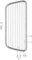
- Fig. 2 is a plan view of the vehicle window glass 1 of the embodiment.
- the vehicle window glass 1 of the present embodiment is used as, for example, a rear window; however, the use of the window glass is not limited to this.
- the lower side of Fig. 1 is towards the outer side of the vehicle, and the upper side is towards the inner side of the vehicle.
- the vehicle window glass 1 includes a glass plate 11, a color ceramic layer (sintered ceramic layer) 12, an electrically conductive layer 13, a lead-free solder 14 and a power supply terminal 15.
- the glass plate 11 has a curved shape acquired by bending processing.
- the glass plate 11 may be produced to have an approximately trapezoidal curved shape.
- the glass plate 11 may also be a tempered glass plate having a compressive stress layer (external pressure application force) formed on the surface by thermally tempering by air jets or a chemically tempering method, or a laminated glass plate obtained by bonding two sheets of glass plates using a resin film.
- a compressive stress layer external pressure application force
- the soda lime silicate glass defined in ISO 16293-1 as well as materials having known glass compositions can be used. Furthermore, as the material for the glass plate 11, a material in which coloring components such as iron and cobalt are appropriately adjusted as components of the glass composition so that the glass plate exhibits color tones such as grey, green, and blue may also be used.
- the color ceramic layer 12 is formed for the purpose of preventing deterioration of a urethane-based adhesive caused by solar radiation from the outside when the vehicle window glass 1 is adhered to the window frame, and for hiding the wiring or the like of the electrically conductive layer 13 formed on the vehicle interior side surface of the vehicle window glass 1 from being seen from the outside.
- a black-colored color ceramic layer is used.
- the color ceramic layer 12 is a color ceramic composition including a heat-resistant pigment (metal oxide) as an inorganic component, and a glass material having a softening point lower than the softening point of the glass plate 11.
- a heat-resistant pigment metal oxide
- a glass material having a softening point lower than the softening point of the glass plate 11.
- composition a composition formed by applying a ceramic paste formed by kneading a powder of a heat-resistant pigment (metal oxide) as an inorganic component and a powder of glass frit as a glass material together with a vehicle, on the surface of the glass plate 11 by screen printing, and calcining the applied ceramic paste, can be used.
- a ceramic paste formed by kneading a powder of a heat-resistant pigment (metal oxide) as an inorganic component and a powder of glass frit as a glass material together with a vehicle, on the surface of the glass plate 11 by screen printing, and calcining the applied ceramic paste.
- a heat-resistant pigment is incorporated in order to impart an intended color to the ceramic color.
- the particle size of the pigment is determined as appropriate in consideration the dispersibility in the ceramic paste or color developability, and a heat-resistant pigment having a 50% particle size of 0.1 to 10 ⁇ m, and preferably about 0.2 to 5 ⁇ m, can be used.
- a conventionally used heat-resistant pigment can be used.
- a pigment for displaying black color examples include a copper-chromium composite oxide, an iron-manganese composite oxide, a copper-chromium-manganese composite oxide, a cobalt-iron-chromium composite oxide, and magnetite.
- a pigment for displaying brown color examples include a zinc-iron composite oxide and a zinc-iron-chromium composite oxide.
- examples of a blue-colored pigment include cobalt blue
- examples of a green-colored pigment include chrome green, a cobalt-zinc-nickel-titanium composite oxide, and a cobalt-aluminum-chromium composite oxide.
- white-colored pigments titanium white, zinc oxide, and the like
- red-colored pigments red iron oxide, and the like
- yellow-colored pigments titanium yellow, a titanium-barium-nickel composite oxide, a titanium-antimony-nickel composite oxide, a titanium-antimony-chromium composite oxide, and the like
- the glass frit is intended for forming the color ceramic layer 12 by binding the color ceramic to the glass plate.
- any glass frit that is conventionally used for color ceramics can be used. Examples of such glass frit include borosilicate-based glass, zinc borosilicate-based glass and bismuth-based glass. These glass frits can be used singly or in combination of two or more kinds thereof.
- the softening point temperature of the glass frit is preferably lower than the bending processing temperature of the glass plate 11, for example, 600°C to 750°C, and a glass frit having a softening point temperature of about 380°C to 600°C, preferably 400°C to 580°C, and more preferably 410°C to 550°C, can also be used.
- the particle size of the glass frit is determined as appropriate in consideration of the coatability of the ceramic paste at the time of screen printing, and for example, a glass frit having a 50% particle size of about 0.1 to 10 ⁇ m, preferably 0.5 to 5 ⁇ m, and more preferably 1 to 4 ⁇ m, can be used.
- the content of the glass material can be adjusted to 50% to 95% by mass, and preferably 60% to 80% by mass. This content can be appropriately adjusted in consideration of the binding property of the color ceramic layer 12 to the glass plate 11 and the color tone of the color ceramic layer 12.
- the color ceramic layer 12 is a calcination product of the glass material and the heat-resistant pigment, and the color ceramic layer 12 becomes a porous body containing pores. It is speculated that since the color ceramic layer 12 becomes a material that is more flexible than the glass 11, stress relief occurs in the color ceramic layer 12 having a predetermined thickness.
- the vehicle is a material incorporated in order to produce a powder of a heat-resistant pigment (metal oxide) as an inorganic component and a powder of glass frit as a glass material into a paste, and to apply the paste in a coating process such as screen printing, and the vehicle includes a dispersing medium and a binder.
- the vehicle is incorporated in an appropriate amount in consideration of printability (coatability), and for example, the vehicle can be incorporated in an amount of 10% to 50% by mass, and preferably 15% to 45% by mass with respect to the total amount of the color ceramic paste.
- the dispersing medium is preferably a medium which has low volatility at normal temperature and has a boiling point such that the dispersing medium volatilizes at a temperature lower than the temperature at which the glass frit is softened.
- a dispersing medium having a boiling point of about 50°C to 250°C can be used.
- the dispersing medium examples include aliphatic alcohols (for example, saturated or unsaturated C6-3 such as 2-ethyl-1-hexanol, octanol, and decanol, and the like, or aliphatic alcohols), cellosolves (C1-4 alkyl cellosolves such as methyl cellosolve, ethyl cellosolve, and butyl cellosolve, and the like), cellosolve acetates (C1-4 alkyl cellosolve acetates such as ethyl cellosolve acetate and butyl cellosolve acetate), carbitols (C1-4 alkyl carbitols such as methyl carbitol, ethyl carbitol, propyl carbitol, and butyl carbitol, and the like), carbitol acetates (C1-4 alkyl cellosolve acetates such as ethyl carbitol acetate and
- any binder capable of imparting adequate viscosity to the color ceramic paste and capable of being decomposed at about 200°C to 550°C, and preferably 220°C to 400°C, may be used.
- thermoplastic resin an olefin-based resin, a vinyl-based resin, an acrylic resin, a styrene-based resin, a polyester-based resin, a polyamide-based resin, a cellulose derivative, and the like
- thermosetting resin a thermosetting acrylic resin, an epoxy resin, a phenolic resin, an unsaturated polyester-based resin, a polyurethane-based resin, and the like
- An acrylic resin is preferred.
- the proportion of the vehicle with respect to the total amount may be 5% to 80% by mass, preferably 10% to 50% by mass, and more preferably 15% to 40% by mass.
- the electrically conductive layer 13 has, as illustrated in Fig. 2 , busbars 13a respectively formed on the color ceramic layer 12 on both lateral edges of the glass plate 11; and wire filaments 13b arranged in parallel at a predetermined distance and connecting the both busbars 13a.
- the electrically conductive layer 13 is a conductor composition including silver metal (silver or a silver alloy), and a glass material having a softening point temperature lower than the softening point temperature of the glass plate 11.
- the composition is formed such that a silver paste containing silver as a main component is applied on the color ceramic layer 12 by screen printing with a predetermined pattern, and the applied material is sintered.
- the electrically conductive layer 13 is, for example, a hot wire print of a defogger or a defroster; however, the electrically conductive layer may also be an antenna print for broadcast reception.
- the color ceramic layer 12 and the electrically conductive layer 13 are sintered together after being screen printed and dried, as described above.
- the silver paste includes a silver powder containing silver or a silver alloy, glass frit that becomes a glass material in the conductor composition, a vehicle and other additives as necessary.
- the content of the silver metal in the conductor composition, and the particle size of the silver powder in the silver paste are determined as appropriate in consideration of the specific resistance of the electrically conductive layer 13.
- the content of silver metal in the conductor composition can be adjusted to, for example, 85% to 99% by mass, and preferably 88% to 98% by mass.
- the other component is substantially formed from a glass material having a softening point lower than the softening point of the glass plate 11, and this glass component can be formed by calcining glass frit.
- a silver powder having a 50% particle size of about 0.1 to 10 ⁇ m, and preferably 0.2 to 7 ⁇ m can be used.
- the glass frit and the vehicle used in the silver paste can be similar to the glass frit and vehicle mentioned in the section for the color ceramic paste, and regarding the mixing proportion of the vehicle, the vehicle can be incorporated at a proportion of 10% to 50% by mass, and preferably 15% to 45% by mass, with respect to the total amount of the paste.
- the conductor composition since it is necessary to secure electrical conductivity of the composition, the percentage content of silver metal needs to be increased, and the conductor composition has a lower percentage content of the glass material compared to the color ceramic layer.
- the object of the present invention may be potentially achievable by producing the electrically conductive layer 13 into a thick film; however, in order to produce the electrically conductive layer 13 into a thick film, it is necessary to apply an ample amount of the silver paste on the glass plate 11.
- Application of the silver paste on the glass plate 11 can be carried out by screen printing; however, for the purpose of increasing the production efficiency, it is preferable that the number of times of printing is set to one time. Therefore, the discharge amount of the silver paste onto the glass plate may be increased by stacking at least two sheets of the screen.
- the lead-free solder 14 joins a defogger hot wire or an antenna wire, formed of the electrically conductive layer 13, with a power supply terminal 15.
- the lead-free solder 14 may be, for example, a Sn-Ag-based lead-free solder or a Sn-Ag-Cu-based lead-free solder, and the examples are not limited to these.
- the lead-free solder 14 contains Ag.
- a lead-free solder containing Sn at a content of 95% by mass or more is used, and the content is adjusted to preferably 95% to 99% by mass, and more preferably 96% to 98% by mass.
- the content of Ag is adjusted to 5% by mass or less, preferably 1.5% to 5% by mass, and more preferably 2% to 4% by mass.
- the lead-free solder contains Cu, the content of Cu can be adjusted to 1.5% by mass or less, and preferably 1% to 0.1% by mass.
- the power supply terminal 15 is connected to a power supply mounted in the automotive vehicle (not shown in the diagram) and is provided in order to supply an electric current to the electrically conductive layer 13.
- a power supply mounted in the automotive vehicle not shown in the diagram
- an electrically conductive material is satisfactory, and a material that can be easily processed by mechanical processing is preferred. For example, copper and brass can be used.
- a structural example of the power supply terminal 15 may be a terminal having a pair of terminal washers 15a that are joined by the lead-free solder 14; a leg 15b that connects these washers; and a site for connecting to an electric cable (not shown in the diagram).
- a vehicle window glass 1 in which a glass plate 11, a color ceramic layer 12, an electrically conductive layer 13, a lead-free solder 14, and a power supply terminal 15 are laminated, is produced.
- the defogger wiring or antenna wiring formed by the electrically conductive layer 13 an electric current is caused to flow through or is cut off via the power supply terminal 15. Thereby, the glass plate 11 is repeatedly heated and cooled. Furthermore, heating and cooling is repeated by the influence of the atmospheric environment.
- the lead-free solder 14 Since the lead-free solder 14 has high elastic modulus and high rigidity compared to conventional leaded solders, it is difficult for the lead-free solder to conform flexibly to the expansion and contraction of the glass plate 11. Therefore, when the thermal expansion coefficient of the lead-free solder is different from the thermal expansion coefficient of the glass plate 11, stress is applied to the glass plate 11 and cracks (fissures, breakage, cracking or the like) are likely to be generated.
- the inventors of the present invention found that even when the lead-free solder 14 is used, in a case in which the layer thicknesses of the color ceramic layer 12 and the electrically conductive layer 13 and the like satisfy predetermined conditions, the glass plate 11 does not easily undergo cracking even if heating and cooling of the glass plate 11 is repeated. In the following description, the experimental results will be explained.
- a color (black) ceramic paste was applied by screen printing on the peripheral edge of a glass plate 11 (flat glass plate measuring 300 mm on each side (thickness 3.5 mm)), and the ceramic paste was dried for 20 minutes at 120°C.
- a precursor coating film of the color ceramic layer 13 was formed into a frame form on the peripheral edge of the glass plate 11.
- a silver paste was applied on the coating film of the precursor of the color ceramic layer 12 and on the glass plate 11 by screen printing, and the silver paste was dried for 10 minutes at 120°C.
- a precursor coating film of the electrically conductive layer 13 was formed.
- the glass plate 11 having various precursor coating films formed thereon was subjected to bending processing and thermal tempering by air jets in a known air-jet tempering furnace, and thus a glass plate 11 having a color ceramic layer 12 and an electrically conductive layer 13 formed thereon was obtained.
- the electrically conductive layer 13 connects busbars 13a, which are formed on the color ceramic layer 12 on both lateral edges of the glass plate 11 and have a width of 18 mm and a length of 250 mm, and wire filaments 13b having a wire width of 0.5 m which connect the two busbars 13a and are arranged in parallel at a distance of 40 mm.
- the thickness of the color ceramic layer 12, the thickness of the electrically conductive layer 13, the surface roughness (Ra) of the electrically conductive layer, and the conditions for screen printing of various Examples and Comparative Examples are as shown in Table 1.
- the quality of the joining part was evaluated by subjecting the vehicle window glass 1 to a cooling-heating cycle resistance test. Specifically, a treatment of 20°C ⁇ - 40°C (90 minutes) ⁇ 20°C ⁇ 105°C (120 minutes) ⁇ 20°C was designated as one cycle, and an observation was made on the presence or absence of crack generation in the glass plate 11 after repeatedly performing 60 cycles.
- the power supply terminal 15 was pulled with a force of 80 N using a push-pull gauge, in a direction perpendicular to the joined surface between the electrically conductive layer 13 and the terminal washer 15a, and thereby the bonding strength of the joined body was measured. A sample in which there was no crack generation in the glass plate 11 and detachment did not occur at the joining part, was determined as a satisfactory product.
- Absent 20 #180 was used twice 13 (Ra:1.3 ⁇ m) (Rz:8.3 ⁇ m) #200+#110, Two kinds of screens were overlapped, and silver paste was applied.
- Absent 18 #110 was used once 7 ⁇ 8 #200 was used once Absent 18 #110 was used once 10 ⁇ 12 #200+#135, Two kinds of screens were overlapped, and silver paste was applied.
- Present 18 #110 was used once 16 ⁇ 17 #200+#110, Two kinds of screens were overlapped, and silver paste was applied.
- Present 10 #180 was used once 7 ⁇ 8 #200 was used once Present 10 #180 was used once 10 ⁇ 12 #200+#135, Two kinds of screens were overlapped, and silver paste was applied.
- Present 10 #180 was used once 16 ⁇ 17 #200+#110, Two kinds of screens were overlapped, and silver paste was applied.
- the number of times of printing is adjusted to one time, and a screen having a mesh opening size of 140 to 180 ⁇ m (preferably 150 to 170 ⁇ m) and a numerical aperture of 40% to 60% (preferably 45% to 55%) is used.
- a screen having a mesh opening of 53 Lo 93 ⁇ m (preferably 63 to 83 ⁇ m) and a numerical aperture of 24% to 39% (preferably 28% to 36%) is used.
- the thickness of the color ceramic layer 12 is larger than 18 mm.
- the thickness of the color ceramic layer 12 is larger than 25 ⁇ m, there is a problem that the production efficiency is decreased.
- the thickness of the color ceramic layer 12 of the present embodiment is more than 18 mm and less than or equal to 25 mm, and more preferably from 18 mm to 22 mm.
- the thickness of the color ceramic layer 12 is 10 ⁇ m and 20 ⁇ m, since the influence of the thickness of the color ceramic layer 12 is strong, the presence or absence of cracks in the glass plate 11 is determined irrespective of the thickness of the electrically conductive layer 13.
- the thickness of the color ceramic layer 12 is 10 ⁇ m
- the stress occurring due to the difference in the thermal expansion between the lead-free solder 14 and the glass plate 11 cannot be buffered, and cracks are generated in the glass plate 11.
- the thickness of the color ceramic layer 12 is 20 ⁇ m, since the color ceramic layer 12 is thick, the stress occurring due to the difference in the thermal expansion between the lead-free solder 14 and the glass plate 11 is buffered, and cracks are not generated in the glass plate 11.
- the thickness of the color ceramic layer 12 is 18 ⁇ m, it may be considered that the influence exerted by the thickness of the color ceramic layer 12 on the presence or absence of cracks in the glass is fluid.
- the state of the electrically conductive layer 13 also affects the presence or absence of cracks in the glass.
- the electrically conductive layer 13 has a thickness of 7 to 8 ⁇ m as a result of performing screen printing once, cracks are not generated in the glass plate 11, and in a case in which the electrically conductive layer has a thickness of 10 ⁇ m or more as a result of performing screen printing twice, cracks are generated in the glass plate 11.
- the electrically conductive layer 13 is such that when the electrically conductive layer 13 is formed by performing coating with two sheets of screens, the surface of the electrically conductive layer 13 becomes rough compared to a case in which the electrically conductive layer 13 is formed by performing coating with one sheet of screen. As the surface becomes rougher, the adhesion between the electrically conductive layer 13 and the lead-free solder 14 becomes strong due to the anchor effect. If the adhesive force becomes too strong, a large amount of stress is exerted on the glass plate 11 due to the difference between the expansion coefficient of the glass plate 11 and the thermal expansion coefficient of the lead-free solder 14, and cracks are likely to be generated.
- the electrically conductive layer 13 when the electrically conductive layer 13 is formed by performing coating with one sheet of screen, the surface of the electrically conductive layer 13 is smooth compared to a case in which the electrically conductive layer 13 is formed by performing coating with two sheets of screens. Therefore, in a case in which the electrically conductive layer is formed by performing coating with one sheet of screen, the adhesive force between the electrically conductive layer 13 and the lead-free solder 14 is weak, compared to a case in which the electrically conductive layer 13 is formed by performing coating with two sheets of screens. Therefore, the stress occurring due to the difference between the expansion coefficient of the glass plate 11 and the thermal expansion coefficient of the lead-free solder 14 is relieved, and cracks are not easily generated in the glass plate 11. Meanwhile, even in this case, the electrically conductive layer 13 and the lead-free solder 14 did not undergo detachment.
- the adhesive force between the electrically conductive layer 13 and the lead-free solder 14 was not so weak as to cause detachment; however, since the adhesive force was weak to the extent that the difference in the thermal expansion between the lead-free solder 14 and the glass plate 11 was just buffered, it is considered that cracks were not generated in the glass plate 11.
- the electrically conductive layer 13 of the embodiment may be considered to have been formed by performing coating with one sheet of screen, in a case in which the thickness of the color ceramic layer 12 is 18 ⁇ m.
- the mesh opening is preferably #200, that is, the numerical aperture is preferably 32%, so that the formation can be achieved with one sheet of screen.
Landscapes
- Chemical & Material Sciences (AREA)
- Engineering & Computer Science (AREA)
- Mechanical Engineering (AREA)
- Materials Engineering (AREA)
- General Chemical & Material Sciences (AREA)
- Geochemistry & Mineralogy (AREA)
- Life Sciences & Earth Sciences (AREA)
- Organic Chemistry (AREA)
- Chemical Kinetics & Catalysis (AREA)
- Dispersion Chemistry (AREA)
- Composite Materials (AREA)
- Surface Treatment Of Glass (AREA)
- Fittings On The Vehicle Exterior For Carrying Loads, And Devices For Holding Or Mounting Articles (AREA)
Description
- The present invention relates to a vehicle window glass and a method for manufacturing a vehicle window glass.
- In regard to vehicle window glasses, for the solder (solder alloy) that connects between a power supply terminal and a wiring formed from a silver paste on a glass plate serving as a base, solder containing lead has been conventionally used. However, in recent years, the influence of lead on the environment and the like have been raised as an issue, and thus transition to the use of lead-free solder is under way. See
WO2012/096373 (EP-A-2664503 ) which describes a vehicle window glass including a glass sheet, a conductor layer formed on the glass sheet (optionally with a black ceramic frame layer between), and a terminal soldered onto a connection part of the conductor layer with lead-free solder. - Lead-free solder has higher Young's modulus and high rigidity compared to leaded solder containing lead. Therefore, when a mechanical stress or a stress caused by the difference in the thermal expansion coefficient is applied, there is a possibility that cracks and the like may be generated in the glass plate, or the solder may be peeled off. In
WO2012/096373 (EP-A-2664503 ) cracking is to be reduced by selecting the solder and conductor layer compositions and forming thin parts of the conductor layer with a narrow width. -
US2015/296569A describes panes such as vehicle window glasses in which a steel alloy compensator plate, of thermal expansion approximated to that of the glass, is laminated between a copper connection element and the lead-free solder layer connecting it to the conductive structure. The conductive structure may lie on a masking screenprint layer. - An object of the present invention is to provide a vehicle window glass that does not easily have cracks generated therein, and a method for manufacturing a vehicle window glass.
- The present invention solves the above-described problems by the following solutions.
- The invention provides a vehicle window glass as set out in the appended claim 1, and a method of manufacturing such a vehicle window glass as set out in the appended claim 7.
- The configuration described above may be improved as appropriate, or at least a portion of the configuration may be replaced with other configurations.
- According to the present invention, we provide a vehicle window glass that does not easily have cracks generated therein, and a method for manufacturing a vehicle window glass.
-
-
Fig. 1 is a cross-sectional view of the vehicle window glass of an embodiment of the present invention. -
Fig. 2 is a plan view of a vehicle window glass 1 of the embodiments. -
Fig. 1 is a cross-sectional view of vehicle window glass 1 of an embodiment of the present invention.Fig. 2 is a plan view of the vehicle window glass 1 of the embodiment. - The vehicle window glass 1 of the present embodiment is used as, for example, a rear window; however, the use of the window glass is not limited to this. When the vehicle window glass 1 illustrated in
Fig. 1 is incorporated into a vehicle, the lower side ofFig. 1 is towards the outer side of the vehicle, and the upper side is towards the inner side of the vehicle. - As illustrated in
Fig. 1 , the vehicle window glass 1 includes aglass plate 11, a color ceramic layer (sintered ceramic layer) 12, an electricallyconductive layer 13, a lead-free solder 14 and apower supply terminal 15. - It is preferable that the
glass plate 11 has a curved shape acquired by bending processing. For example, when theglass plate 11 is used as a rear window glass, the glass plate may be produced to have an approximately trapezoidal curved shape. - The
glass plate 11 may also be a tempered glass plate having a compressive stress layer (external pressure application force) formed on the surface by thermally tempering by air jets or a chemically tempering method, or a laminated glass plate obtained by bonding two sheets of glass plates using a resin film. - Regarding the material for the
glass plate 11, the soda lime silicate glass defined in ISO 16293-1 as well as materials having known glass compositions can be used. Furthermore, as the material for theglass plate 11, a material in which coloring components such as iron and cobalt are appropriately adjusted as components of the glass composition so that the glass plate exhibits color tones such as grey, green, and blue may also be used. - The color
ceramic layer 12 is formed for the purpose of preventing deterioration of a urethane-based adhesive caused by solar radiation from the outside when the vehicle window glass 1 is adhered to the window frame, and for hiding the wiring or the like of the electricallyconductive layer 13 formed on the vehicle interior side surface of the vehicle window glass 1 from being seen from the outside. Preferably a black-colored color ceramic layer is used. - The color
ceramic layer 12 is a color ceramic composition including a heat-resistant pigment (metal oxide) as an inorganic component, and a glass material having a softening point lower than the softening point of theglass plate 11. - As the composition, a composition formed by applying a ceramic paste formed by kneading a powder of a heat-resistant pigment (metal oxide) as an inorganic component and a powder of glass frit as a glass material together with a vehicle, on the surface of the
glass plate 11 by screen printing, and calcining the applied ceramic paste, can be used. - A heat-resistant pigment is incorporated in order to impart an intended color to the ceramic color. The particle size of the pigment is determined as appropriate in consideration the dispersibility in the ceramic paste or color developability, and a heat-resistant pigment having a 50% particle size of 0.1 to 10 µm, and preferably about 0.2 to 5 µm, can be used.
- Regarding the heat-resistant pigment, a conventionally used heat-resistant pigment can be used. Examples of a pigment for displaying black color include a copper-chromium composite oxide, an iron-manganese composite oxide, a copper-chromium-manganese composite oxide, a cobalt-iron-chromium composite oxide, and magnetite. Examples of a pigment for displaying brown color include a zinc-iron composite oxide and a zinc-iron-chromium composite oxide.
- Furthermore, examples of a blue-colored pigment include cobalt blue, and examples of a green-colored pigment include chrome green, a cobalt-zinc-nickel-titanium composite oxide, and a cobalt-aluminum-chromium composite oxide.
- In addition to these pigments, white-colored pigments (titanium white, zinc oxide, and the like), red-colored pigments (red iron oxide, and the like), and yellow-colored pigments (titanium yellow, a titanium-barium-nickel composite oxide, a titanium-antimony-nickel composite oxide, a titanium-antimony-chromium composite oxide, and the like) can also be used.
- The glass frit is intended for forming the color
ceramic layer 12 by binding the color ceramic to the glass plate. Regarding the glass frit, any glass frit that is conventionally used for color ceramics can be used. Examples of such glass frit include borosilicate-based glass, zinc borosilicate-based glass and bismuth-based glass. These glass frits can be used singly or in combination of two or more kinds thereof. - The softening point temperature of the glass frit is preferably lower than the bending processing temperature of the
glass plate 11, for example, 600°C to 750°C, and a glass frit having a softening point temperature of about 380°C to 600°C, preferably 400°C to 580°C, and more preferably 410°C to 550°C, can also be used. - The particle size of the glass frit is determined as appropriate in consideration of the coatability of the ceramic paste at the time of screen printing, and for example, a glass frit having a 50% particle size of about 0.1 to 10 µm, preferably 0.5 to 5 µm, and more preferably 1 to 4 µm, can be used.
- In regard to the color
ceramic layer 12, the content of the glass material (sintered glass frit) can be adjusted to 50% to 95% by mass, and preferably 60% to 80% by mass. This content can be appropriately adjusted in consideration of the binding property of the colorceramic layer 12 to theglass plate 11 and the color tone of the colorceramic layer 12. - The reason why the stress exerted on the
glass plate 11 by the lead-free solder 14 can be relieved by interposing a colorceramic layer 12 having a predetermined thickness therebetween, is not clearly understood. The colorceramic layer 12 is a calcination product of the glass material and the heat-resistant pigment, and the colorceramic layer 12 becomes a porous body containing pores. It is speculated that since the colorceramic layer 12 becomes a material that is more flexible than theglass 11, stress relief occurs in the colorceramic layer 12 having a predetermined thickness. - The vehicle is a material incorporated in order to produce a powder of a heat-resistant pigment (metal oxide) as an inorganic component and a powder of glass frit as a glass material into a paste, and to apply the paste in a coating process such as screen printing, and the vehicle includes a dispersing medium and a binder. The vehicle is incorporated in an appropriate amount in consideration of printability (coatability), and for example, the vehicle can be incorporated in an amount of 10% to 50% by mass, and preferably 15% to 45% by mass with respect to the total amount of the color ceramic paste.
- The dispersing medium is preferably a medium which has low volatility at normal temperature and has a boiling point such that the dispersing medium volatilizes at a temperature lower than the temperature at which the glass frit is softened. For example, a dispersing medium having a boiling point of about 50°C to 250°C can be used.
- Examples of the dispersing medium include aliphatic alcohols (for example, saturated or unsaturated C6-3 such as 2-ethyl-1-hexanol, octanol, and decanol, and the like, or aliphatic alcohols), cellosolves (C1-4 alkyl cellosolves such as methyl cellosolve, ethyl cellosolve, and butyl cellosolve, and the like), cellosolve acetates (C1-4 alkyl cellosolve acetates such as ethyl cellosolve acetate and butyl cellosolve acetate), carbitols (C1-4 alkyl carbitols such as methyl carbitol, ethyl carbitol, propyl carbitol, and butyl carbitol, and the like), carbitol acetates (C1-4 alkyl cellosolve acetates such as ethyl carbitol acetate and butyl carbitol acetate), aliphatic polyhydric alcohols (for example, ethylene glycol, diethylene glycol, dipropylene glycol, 1,4-butanediol, triethylene glycol, and glycerin), alicyclic alcohols such as [for example, cycloalkanols such as cyclohexanol; and terpene alcohols (for example, monoterpene alcohol) such as 1-terpineol and dihydroterpineol], aromatic carboxylic acid esters (phthalic acid di-C1-10 alkyl esters such as dibutyl phthalate and dioctyl phthalate; phthalic acid di-C1-10 alkyl aralkyl esters such as dibutyl benzyl phthalate; and the like), and mixtures thereof.
- Regarding the binder, any binder capable of imparting adequate viscosity to the color ceramic paste and capable of being decomposed at about 200°C to 550°C, and preferably 220°C to 400°C, may be used.
- Examples thereof include a thermoplastic resin (an olefin-based resin, a vinyl-based resin, an acrylic resin, a styrene-based resin, a polyester-based resin, a polyamide-based resin, a cellulose derivative, and the like), a thermosetting resin (a thermosetting acrylic resin, an epoxy resin, a phenolic resin, an unsaturated polyester-based resin, a polyurethane-based resin, and the like), and mixtures thereof. An acrylic resin is preferred. The proportion of the vehicle with respect to the total amount may be 5% to 80% by mass, preferably 10% to 50% by mass, and more preferably 15% to 40% by mass.
- The electrically
conductive layer 13 has, as illustrated inFig. 2 ,busbars 13a respectively formed on thecolor ceramic layer 12 on both lateral edges of theglass plate 11; andwire filaments 13b arranged in parallel at a predetermined distance and connecting the bothbusbars 13a. - The electrically
conductive layer 13 is a conductor composition including silver metal (silver or a silver alloy), and a glass material having a softening point temperature lower than the softening point temperature of theglass plate 11. The composition is formed such that a silver paste containing silver as a main component is applied on thecolor ceramic layer 12 by screen printing with a predetermined pattern, and the applied material is sintered. The electricallyconductive layer 13 is, for example, a hot wire print of a defogger or a defroster; however, the electrically conductive layer may also be an antenna print for broadcast reception. - The
color ceramic layer 12 and the electricallyconductive layer 13 are sintered together after being screen printed and dried, as described above. - The silver paste includes a silver powder containing silver or a silver alloy, glass frit that becomes a glass material in the conductor composition, a vehicle and other additives as necessary.
- The content of the silver metal in the conductor composition, and the particle size of the silver powder in the silver paste are determined as appropriate in consideration of the specific resistance of the electrically
conductive layer 13. The content of silver metal in the conductor composition can be adjusted to, for example, 85% to 99% by mass, and preferably 88% to 98% by mass. - The other component is substantially formed from a glass material having a softening point lower than the softening point of the
glass plate 11, and this glass component can be formed by calcining glass frit. Regarding the particle size of the silver powder, a silver powder having a 50% particle size of about 0.1 to 10 µm, and preferably 0.2 to 7 µm can be used. - Regarding the glass frit and the vehicle used in the silver paste, those applied can be similar to the glass frit and vehicle mentioned in the section for the color ceramic paste, and regarding the mixing proportion of the vehicle, the vehicle can be incorporated at a proportion of 10% to 50% by mass, and preferably 15% to 45% by mass, with respect to the total amount of the paste.
- In regard to the conductor composition, since it is necessary to secure electrical conductivity of the composition, the percentage content of silver metal needs to be increased, and the conductor composition has a lower percentage content of the glass material compared to the color ceramic layer. The object of the present invention may be potentially achievable by producing the electrically
conductive layer 13 into a thick film; however, in order to produce the electricallyconductive layer 13 into a thick film, it is necessary to apply an ample amount of the silver paste on theglass plate 11. Application of the silver paste on theglass plate 11 can be carried out by screen printing; however, for the purpose of increasing the production efficiency, it is preferable that the number of times of printing is set to one time. Therefore, the discharge amount of the silver paste onto the glass plate may be increased by stacking at least two sheets of the screen. When application is achieved according to this method, production of the electricallyconductive layer 13 into a thick film accelerates surface roughening of the electrically conductive layer surface. - Surface roughening of the surface of the electrically
conductive layer 13 allows firm joining of the lead-free solder 14 to the electrically conductive layer by the anchor effect. Then, the stress exerted by the lead-free solder 14 on theglass plate 11 becomes larger. When the production efficiency is considered, and production of thecolor ceramic layer 12 into a thick film is attempted, consequently, cracks tend to be produced in theglass plate 11 in the vehicle window glass 1. When this is considered, the thickness of the electricallyconductive layer 13 be adjusted to 7 to 8 mm. With this thickness, the electricallyconductive layer 13 can be formed highly efficiently without causing surface roughening of the electricallyconductive layer 13. - The lead-
free solder 14 joins a defogger hot wire or an antenna wire, formed of the electricallyconductive layer 13, with apower supply terminal 15. - The lead-
free solder 14 may be, for example, a Sn-Ag-based lead-free solder or a Sn-Ag-Cu-based lead-free solder, and the examples are not limited to these. However, in order to suppress silver solder erosion of the silver wire caused by lead-free solder 14, that is, in order to prevent silver in the electricallyconductive layer 13 from diffusing into the lead-free solder 14 and to prevent the percentage content of silver in the electricallyconductive layer 14 from decreasing, it is preferable that the lead-free solder 14 contains Ag. - Among lead-free solders, a lead-free solder containing Sn at a content of 95% by mass or more is used, and the content is adjusted to preferably 95% to 99% by mass, and more preferably 96% to 98% by mass. The content of Ag is adjusted to 5% by mass or less, preferably 1.5% to 5% by mass, and more preferably 2% to 4% by mass. When the lead-free solder contains Cu, the content of Cu can be adjusted to 1.5% by mass or less, and preferably 1% to 0.1% by mass.
- The
power supply terminal 15 is connected to a power supply mounted in the automotive vehicle (not shown in the diagram) and is provided in order to supply an electric current to the electricallyconductive layer 13. Regarding the material for the terminal 15, an electrically conductive material is satisfactory, and a material that can be easily processed by mechanical processing is preferred. For example, copper and brass can be used. - A structural example of the
power supply terminal 15 may be a terminal having a pair ofterminal washers 15a that are joined by the lead-free solder 14; aleg 15b that connects these washers; and a site for connecting to an electric cable (not shown in the diagram). - In this manner, a vehicle window glass 1 in which a
glass plate 11, acolor ceramic layer 12, an electricallyconductive layer 13, a lead-free solder 14, and apower supply terminal 15 are laminated, is produced. - Here, in the defogger wiring or antenna wiring formed by the electrically
conductive layer 13, an electric current is caused to flow through or is cut off via thepower supply terminal 15. Thereby, theglass plate 11 is repeatedly heated and cooled. Furthermore, heating and cooling is repeated by the influence of the atmospheric environment. - Since the lead-
free solder 14 has high elastic modulus and high rigidity compared to conventional leaded solders, it is difficult for the lead-free solder to conform flexibly to the expansion and contraction of theglass plate 11. Therefore, when the thermal expansion coefficient of the lead-free solder is different from the thermal expansion coefficient of theglass plate 11, stress is applied to theglass plate 11 and cracks (fissures, breakage, cracking or the like) are likely to be generated. - As explained above, the inventors of the present invention found that even when the lead-
free solder 14 is used, in a case in which the layer thicknesses of thecolor ceramic layer 12 and the electricallyconductive layer 13 and the like satisfy predetermined conditions, theglass plate 11 does not easily undergo cracking even if heating and cooling of theglass plate 11 is repeated. In the following description, the experimental results will be explained. - A color (black) ceramic paste was applied by screen printing on the peripheral edge of a glass plate 11 (flat glass plate measuring 300 mm on each side (thickness 3.5 mm)), and the ceramic paste was dried for 20 minutes at 120°C. Thus, a precursor coating film of the
color ceramic layer 13 was formed into a frame form on the peripheral edge of theglass plate 11. - Subsequently, a silver paste was applied on the coating film of the precursor of the
color ceramic layer 12 and on theglass plate 11 by screen printing, and the silver paste was dried for 10 minutes at 120°C. Thus, a precursor coating film of the electricallyconductive layer 13 was formed. - The
glass plate 11 having various precursor coating films formed thereon was subjected to bending processing and thermal tempering by air jets in a known air-jet tempering furnace, and thus aglass plate 11 having acolor ceramic layer 12 and an electricallyconductive layer 13 formed thereon was obtained. - The electrically
conductive layer 13 connectsbusbars 13a, which are formed on thecolor ceramic layer 12 on both lateral edges of theglass plate 11 and have a width of 18 mm and a length of 250 mm, andwire filaments 13b having a wire width of 0.5 m which connect the twobusbars 13a and are arranged in parallel at a distance of 40 mm. - The thickness of the
color ceramic layer 12, the thickness of the electricallyconductive layer 13, the surface roughness (Ra) of the electrically conductive layer, and the conditions for screen printing of various Examples and Comparative Examples are as shown in Table 1. - The lead-
free solder 14, in which Sn (98% by mass)-Ag (2% by mass) is contained in an amount of 0.3 to 0.6 g, is heated to be adhered to theterminal washer 15a of thepower supply terminal 15. - Subsequently, a flux was applied on the lead-
free solder 14, the lead-free solder 14 on the electrically conductive layer 13 (busbar 13a) was locally heated, and thereby joining of thepower supply terminal 15 to the electrically conductive layer 13 (busbar 13a) through the lead-free solder 14 was performed. - In the present Example, a flat glass plate was used as an experiment for examining the influence of the lead-
free solder 14 on theglass plate 11; however, it is needless to say that similar results can also be obtained even with a three-dimensionally bending-processed glass plate, which is used as a vehicle glass. - The quality of the joining part was evaluated by subjecting the vehicle window glass 1 to a cooling-heating cycle resistance test. Specifically, a treatment of 20°C → - 40°C (90 minutes) → 20°C → 105°C (120 minutes) → 20°C was designated as one cycle, and an observation was made on the presence or absence of crack generation in the
glass plate 11 after repeatedly performing 60 cycles. - Furthermore, the
power supply terminal 15 was pulled with a force of 80 N using a push-pull gauge, in a direction perpendicular to the joined surface between the electricallyconductive layer 13 and theterminal washer 15a, and thereby the bonding strength of the joined body was measured. A sample in which there was no crack generation in theglass plate 11 and detachment did not occur at the joining part, was determined as a satisfactory product. - The test results are shown below.
Table 1 Layer thickness of color ceramic layer, µm Type of mesh and number of times of screen printing for color ceramic layer Layer thickness of electrically conductive layer, µm Type of mesh and number of times of screen printing for electrically conductive layer Presence or absence of cracks in glass plate 20 #180 was used twice 7∼8 (Ra:1.0µm) (Rz:6.4µm) #200 was used once Absent 20 #180 was used twice 10 (Ra: 1.1 µm) (Rz:7.3µm) #200+#135, Two kinds of screens were overlapped, and silver paste was applied. Absent 20 #180 was used twice 13 (Ra:1.3µm) (Rz:8.3µm) #200+#110, Two kinds of screens were overlapped, and silver paste was applied. Absent 18 #110 was used once 7∼8 #200 was used once Absent 18 #110 was used once 10∼12 #200+#135, Two kinds of screens were overlapped, and silver paste was applied. Present 18 #110 was used once 16∼17 #200+#110, Two kinds of screens were overlapped, and silver paste was applied. Present 10 #180 was used once 7∼8 #200 was used once Present 10 #180 was used once 10∼12 #200+#135, Two kinds of screens were overlapped, and silver paste was applied. Present 10 #180 was used once 16∼17 #200+#110, Two kinds of screens were overlapped, and silver paste was applied. Present - For the screens, smart meshes produced by Nippon Tokushu Fabric, Inc. were used. The types of meshes, namely #110, #135, #180, and #200, are screen mesh standards, and the numbers each represent the number of lines in a square measuring 1 inch (25.4 mm) on each of four sides. For the screens thus used, the line width, mesh opening (distance between lines), and numerical aperture of the screens were as follows.
Table 2 Lines in 1-inch square Line width of screen Mesh opening Numerical aperture #110 71µm 160µm 48% #135 54µm 134µm 51% #180 54µm 87µm 38% #200 54µm 73µm 32% - In a case in which the line widths of screens are the same, as the number of lines that constitute the mesh is larger, the screen becomes compact, and the amount of discharging the paste onto the glass tends to decrease.
- Meanwhile, it can be seen that in order to form the
color ceramic layer 12, it is preferable that the number of times of printing is adjusted to one time, and a screen having a mesh opening size of 140 to 180 µm (preferably 150 to 170 µm) and a numerical aperture of 40% to 60% (preferably 45% to 55%) is used. Furthermore, in order to form the electricallyconductive layer 13, it is preferable that the number of times of printing is adjusted to one time, and a screen having a mesh opening of 53 Lo 93 µm (preferably 63 to 83 µm) and a numerical aperture of 24% to 39% (preferably 28% to 36%) is used. - As shown in the table, in a case in which the thickness of the
color ceramic layer 12 was 10 µm (#180 was used once), cracks were generated in theglass plate 11, irrespective of the layer thickness of the electricallyconductive layer 13. - In a case in which the thickness of the
color ceramic layer 12 was 18 µm (#110 was used once), cracks were not generated in theglass plate 11 when the layer thickness of the electricallyconductive layer 13 was 7 to 8 µm; however, when the layer thickness of the electricallyconductive layer 13 was 10 µm or more, cracks were generated in theglass plate 11. - In a case in which the thickness of the
color ceramic layer 12 was 20 µm (#180 was used twice), cracks were not generated in theglass plate 11, irrespective of the layer thickness of the electricallyconductive layer 13. - It was found that in a case in which the
color ceramic layer 12 was 10 µm (#180 was used once), cracks were generated irrespective of the thickness of the electricallyconductive layer 13 or the number of times of screen printing. - Therefore, the thickness of the
color ceramic layer 12 is larger than 18 mm. - Meanwhile, when the thickness of the
color ceramic layer 12 is larger than 25 µm, there is a problem that the production efficiency is decreased. - Therefore, the thickness of the
color ceramic layer 12 of the present embodiment is more than 18 mm and less than or equal to 25 mm, and more preferably from 18 mm to 22 mm. - A case in which the thickness of the
ceramic layer 12 becomes 10 µm occurs when #180 is used once. That is, when the numerical aperture is 38%. Therefore, it is preferable that the numerical aperture is higher than 38%. - A case in which the thickness of the
ceramic layer 12 becomes 18 µm occurs when #110 is used once. That is, since the numerical aperture is 48%, it is more preferable that the numerical aperture is 48% or higher. - In addition, a case in which the thickness of the
ceramic layer 12 becomes 25 µm occurs when the numerical aperture is 60% or higher. - As explained above, in a case in which the thickness of the
color ceramic layer 12 was 10 µm, cracks were generated in theglass plate 11, irrespective of the layer thickness of the electricallyconductive layer 13. - In a case in which the thickness of the
color ceramic layer 12 was 18 µm, cracks were not generated in theglass plate 11 when the layer thickness of the electricallyconductive layer 13 was 7 to 8 µm, however, when the layer thickness of the electricallyconductive layer 13 was 10 µm or more, cracks were generated in theglass plate 11. - In a case in which the thickness of the
color ceramic layer 12 was 20 µm, cracks were not generated in theglass plate 11 irrespective of the layer thickness of the electricallyconductive layer 13. - It is speculated that in a case in which the thickness of the
color ceramic layer 12 is 10 µm and 20 µm, since the influence of the thickness of thecolor ceramic layer 12 is strong, the presence or absence of cracks in theglass plate 11 is determined irrespective of the thickness of the electricallyconductive layer 13. - That is, in a case in which the thickness of the
color ceramic layer 12 is 10 µm, since thecolor ceramic layer 12 is thin, the stress occurring due to the difference in the thermal expansion between the lead-free solder 14 and theglass plate 11 cannot be buffered, and cracks are generated in theglass plate 11. - In a case in which the thickness of the
color ceramic layer 12 is 20 µm, since thecolor ceramic layer 12 is thick, the stress occurring due to the difference in the thermal expansion between the lead-free solder 14 and theglass plate 11 is buffered, and cracks are not generated in theglass plate 11. - Meanwhile, in a case in which the thickness of the
color ceramic layer 12 is 18 µm, it may be considered that the influence exerted by the thickness of thecolor ceramic layer 12 on the presence or absence of cracks in the glass is fluid. - Therefore, the state of the electrically
conductive layer 13 also affects the presence or absence of cracks in the glass. Thus, it may be considered that in a case in which the electricallyconductive layer 13 has a thickness of 7 to 8 µm as a result of performing screen printing once, cracks are not generated in theglass plate 11, and in a case in which the electrically conductive layer has a thickness of 10 µm or more as a result of performing screen printing twice, cracks are generated in theglass plate 11. - It is speculated that this is affected by the number of sheets of screens stacked when the electrically
conductive layer 13 is formed. - The electrically
conductive layer 13 is such that when the electricallyconductive layer 13 is formed by performing coating with two sheets of screens, the surface of the electricallyconductive layer 13 becomes rough compared to a case in which the electricallyconductive layer 13 is formed by performing coating with one sheet of screen. As the surface becomes rougher, the adhesion between the electricallyconductive layer 13 and the lead-free solder 14 becomes strong due to the anchor effect. If the adhesive force becomes too strong, a large amount of stress is exerted on theglass plate 11 due to the difference between the expansion coefficient of theglass plate 11 and the thermal expansion coefficient of the lead-free solder 14, and cracks are likely to be generated. - On the other hand, when the electrically
conductive layer 13 is formed by performing coating with one sheet of screen, the surface of the electricallyconductive layer 13 is smooth compared to a case in which the electricallyconductive layer 13 is formed by performing coating with two sheets of screens. Therefore, in a case in which the electrically conductive layer is formed by performing coating with one sheet of screen, the adhesive force between the electricallyconductive layer 13 and the lead-free solder 14 is weak, compared to a case in which the electricallyconductive layer 13 is formed by performing coating with two sheets of screens. Therefore, the stress occurring due to the difference between the expansion coefficient of theglass plate 11 and the thermal expansion coefficient of the lead-free solder 14 is relieved, and cracks are not easily generated in theglass plate 11. Meanwhile, even in this case, the electricallyconductive layer 13 and the lead-free solder 14 did not undergo detachment. - That is, the adhesive force between the electrically
conductive layer 13 and the lead-free solder 14 was not so weak as to cause detachment; however, since the adhesive force was weak to the extent that the difference in the thermal expansion between the lead-free solder 14 and theglass plate 11 was just buffered, it is considered that cracks were not generated in theglass plate 11. - Therefore, the electrically
conductive layer 13 of the embodiment may be considered to have been formed by performing coating with one sheet of screen, in a case in which the thickness of thecolor ceramic layer 12 is 18 µm. - In order to form the electrically
conductive layer 13, the mesh opening is preferably #200, that is, the numerical aperture is preferably 32%, so that the formation can be achieved with one sheet of screen. -
- (1) The vehicle window glass 1 of the present embodiments includes a
glass plate 11; acolor ceramic layer 12 formed on the surface of theglass plate 11; and a electricallyconductive layer 13 formed on the surface of thecolor ceramic layer 12 and containing silver as a main component, and the electricallyconductive layer 13 is connected to a terminal 15 through which electricity is conducted to the electrically conductive layer 3, by means of a lead-free solder 14. The thickness of thecolor ceramic layer 12 is more than 18 mm and less than or equal to 25 mm. - (2) When the thickness of the
color ceramic layer 12 is 18 mm or larger, crack generation occurs with more difficulty. Furthermore, when the thickness of thecolor ceramic layer 12 is 20 mm or more, cracks are generated in the glassplate 1 with even more difficulty. - (3) Since the thickness of the
color ceramic layer 12 of the vehicle window glass 1 of the embodiments is 18 mm, and the electricallyconductive layer 13 is formed by performing coating with one sheet of screen, cracks are not easily generated in the glass plate 1. - (4) Since the electrically
conductive layer 13 of the vehicle window glass 1 of the embodiments is such that when the thickness of thecolor ceramic layer 12 is 18 mm, the layer thickness of the electrically conductive layer is 7 to 8 mm, cracks are not easily generated in the glass plate 1. - 1: Vehicle window glass, 11: glass plate, 12: color ceramic layer, 13: electrically conductive layer, 14: lead-free solder, 15: power supply terminal
Claims (8)
- A vehicle window glass in which the following are laminated:a glass plate (11);a color ceramic layer (12) formed on the surface of the glass plate (11);an electrically conductive layer (13) formed on the surface of the color ceramic layer (12) and containing silver as a main component, anda terminal (15) through which electricity is conducted, connected to the electrically conductive layer (13) by means of the lead-free solder (14);characterized in thatthe color ceramic layer (12) has a layer thickness of 18 µm or more and less than or equal to 25 µm, andthe electrically conductive layer (13) has a layer thickness of 7 µm or more and less than or equal to 8 µm.
- A vehicle window glass according to claim 1,
wherein the color ceramic layer (12) is a black-colored color ceramic layer (12). - A vehicle window glass according to any one of the preceding claims
wherein the electrically conductive layer (13) is formed by performing coating with one sheet of screen. - A vehicle window glass according to any one of the preceding claims
wherein the electrically conductive layer (13) has busbars (13a) respectively formed on the color ceramic layer (12) at both of lateral edges of the glass plate (11), and wire filaments (13b) arranged in parallel at predetermined distance and connecting the busbars (13a). - A vehicle window glass according to any one of the preceding claims
wherein the lead-free solder (14) is Sn-Ag-based lead-free solder or Sn-Ag-Cu-based lead-free solder. - A vehicle window glass according to any one of the preceding claims
wherein the terminal (15) is of copper or brass. - A method for manufacturing the vehicle window glass according to any one of claims 1 to 6, the method comprising:a step of printing a ceramic paste on the glass plate with a screen having a numerical aperture of larger than 38% and smaller than 60%, thereby forming a coating film of a precursor of the color ceramic layer (12); anda step of printing a silver paste on the coating film of a precursor of the color ceramic layer with one sheet of screen.
- A method according to claim 7,
wherein the number of times of printing with the ceramic paste to form said coating film is one time.
Applications Claiming Priority (2)
| Application Number | Priority Date | Filing Date | Title |
|---|---|---|---|
| JP2016010348A JP6613920B2 (en) | 2016-01-22 | 2016-01-22 | VEHICLE WINDOW GLASS AND METHOD FOR PRODUCING VEHICLE WINDOW GLASS |
| PCT/JP2016/083669 WO2017126202A1 (en) | 2016-01-22 | 2016-11-14 | Vehicle window glass and method for manufacturing vehicle window glass |
Publications (4)
| Publication Number | Publication Date |
|---|---|
| EP3369596A1 EP3369596A1 (en) | 2018-09-05 |
| EP3369596A4 EP3369596A4 (en) | 2018-12-12 |
| EP3369596B1 EP3369596B1 (en) | 2021-04-14 |
| EP3369596B2 true EP3369596B2 (en) | 2024-02-28 |
Family
ID=59361580
Family Applications (1)
| Application Number | Title | Priority Date | Filing Date |
|---|---|---|---|
| EP16886441.1A Active EP3369596B2 (en) | 2016-01-22 | 2016-11-14 | Vehicle window glass and method for manufacturing vehicle window glass |
Country Status (5)
| Country | Link |
|---|---|
| US (1) | US10696582B2 (en) |
| EP (1) | EP3369596B2 (en) |
| JP (1) | JP6613920B2 (en) |
| CN (1) | CN108367657B (en) |
| WO (1) | WO2017126202A1 (en) |
Families Citing this family (3)
| Publication number | Priority date | Publication date | Assignee | Title |
|---|---|---|---|---|
| MA53152A (en) * | 2018-07-20 | 2021-05-26 | Saint Gobain | DEVICE AND METHOD FOR BRAZING ELEMENTS IN CONTACT WITH INDUCTION HEAT |
| JPWO2022176814A1 (en) * | 2021-02-19 | 2022-08-25 | ||
| US20240239275A1 (en) * | 2021-05-18 | 2024-07-18 | Corning Incorporated | Vehicle interior component having high surface energy bonding interface and methods of forming same |
Family Cites Families (17)
| Publication number | Priority date | Publication date | Assignee | Title |
|---|---|---|---|---|
| JPS61111939A (en) * | 1984-11-02 | 1986-05-30 | Nippon Sheet Glass Co Ltd | Plate glass |
| US4623389A (en) * | 1985-04-22 | 1986-11-18 | Ppg Industries, Inc. | Electroconductive silver composition |
| US5817586A (en) * | 1996-04-12 | 1998-10-06 | Asahi Glass Company Ltd. | Colored ceramic composition |
| CN100500360C (en) * | 2004-08-10 | 2009-06-17 | 旭硝子株式会社 | Window glass for vehicle |
| US7223940B2 (en) * | 2005-02-22 | 2007-05-29 | Ppg Industries Ohio, Inc. | Heatable windshield |
| US20090053534A1 (en) | 2007-08-21 | 2009-02-26 | Robert Prunchak | Coating compositions |
| CN101970371A (en) * | 2008-02-13 | 2011-02-09 | 日本板硝子株式会社 | Window pane with sintered conductive ceramic |
| JPWO2010131595A1 (en) * | 2009-05-14 | 2012-11-01 | 日本板硝子株式会社 | GLASS FOR VEHICLE AND METHOD FOR MANUFACTURING THE SAME |
| JP2012091216A (en) * | 2010-10-28 | 2012-05-17 | Asahi Glass Co Ltd | Lead-free solder alloy and glass article using the same |
| JP5830033B2 (en) * | 2010-12-28 | 2015-12-09 | 日本板硝子株式会社 | Glass substrate with pattern and method for manufacturing the same |
| KR20140032973A (en) | 2011-01-14 | 2014-03-17 | 아사히 가라스 가부시키가이샤 | Windowpane for vehicles and method for producing same |
| EP2671666B1 (en) * | 2011-03-02 | 2016-07-20 | Central Glass Company, Limited | Lead-free solder alloy for vehicle glass |
| JP2014096198A (en) * | 2011-03-02 | 2014-05-22 | Central Glass Co Ltd | Method of bonding window pane for automobiles and feeding terminal |
| US20130115435A1 (en) * | 2011-11-04 | 2013-05-09 | GM Global Technology Operations LLC | Laminated windshield glass |
| EP2923529B1 (en) * | 2012-11-21 | 2016-12-07 | Saint-Gobain Glass France | Disc with electric connection element and compensator plates |
| AR097558A1 (en) | 2013-10-29 | 2016-03-23 | Saint Gobain | ENTREPAÑO WITH - AT LEAST - TWO ELEMENTS OF ELECTRICAL CONNECTION AND A CONNECTOR |
| CN106507693B (en) | 2014-04-29 | 2020-03-17 | 法国圣戈班玻璃厂 | Electrical connection element for contacting an electrically conductive structure on a substrate |
-
2016
- 2016-01-22 JP JP2016010348A patent/JP6613920B2/en active Active
- 2016-11-14 EP EP16886441.1A patent/EP3369596B2/en active Active
- 2016-11-14 CN CN201680073953.8A patent/CN108367657B/en active Active
- 2016-11-14 WO PCT/JP2016/083669 patent/WO2017126202A1/en unknown
- 2016-11-14 US US16/062,506 patent/US10696582B2/en active Active
Also Published As
| Publication number | Publication date |
|---|---|
| CN108367657A (en) | 2018-08-03 |
| JP2017128287A (en) | 2017-07-27 |
| EP3369596A4 (en) | 2018-12-12 |
| EP3369596B1 (en) | 2021-04-14 |
| WO2017126202A1 (en) | 2017-07-27 |
| JP6613920B2 (en) | 2019-12-04 |
| US20190002338A1 (en) | 2019-01-03 |
| EP3369596A1 (en) | 2018-09-05 |
| CN108367657B (en) | 2021-10-01 |
| US10696582B2 (en) | 2020-06-30 |
Similar Documents
| Publication | Publication Date | Title |
|---|---|---|
| EP2664503B1 (en) | A method for producing a windowpane for vehicles | |
| EP2832704B1 (en) | Ceramic color paste, ceramic color, glass having ceramic color | |
| JP3541070B2 (en) | Automotive glass thick film conductor paste | |
| EP3369596B2 (en) | Vehicle window glass and method for manufacturing vehicle window glass | |
| JP4976508B2 (en) | Window glass with conductive ceramic sintered body | |
| US20090098350A1 (en) | Conductor composition v | |
| JP7037047B2 (en) | Vehicle window glass | |
| JPWO2006132319A1 (en) | Glass article on which conductive film is formed and method for producing the same | |
| JP5827318B2 (en) | Soldering in thin glass sheets | |
| JP2020037404A (en) | Vehicle window glass | |
| US5352479A (en) | Method for forming an electrode | |
| JP2021517715A (en) | Manufacturing method of glass assembly for vehicles | |
| CN102870210A (en) | Substrate on which element is to be mounted, and process for production thereof | |
| JP2024515695A (en) | Enamel paste composition, enamel coating product, and method for producing same | |
| JP5600458B2 (en) | Manufacturing method of glass plate provided with transfer-type film for baking and fired body | |
| CN101669175A (en) | Emi shield glass with blackened conductive pattern and a method for preparation thereof | |
| WO2022172785A1 (en) | Solder bonded structure, windowpane for vehicles, method for producing solder bonded structure, method for producing glass article, and glass article | |
| CN111902239A (en) | Method for producing vehicle glass component | |
| CN220730582U (en) | Electrochromic device | |
| KR20120007231A (en) | Ag paste for glass of vehicle and glass of vehicle manufactured by using the same | |
| CN116880108A (en) | Electrochromic device and preparation method thereof | |
| JPWO2010150832A1 (en) | Window glass with conductive ceramic sintered body and method for manufacturing the same | |
| GB2327839A (en) | Terminating electrical circuits on glazing panels |
Legal Events
| Date | Code | Title | Description |
|---|---|---|---|
| STAA | Information on the status of an ep patent application or granted ep patent |
Free format text: STATUS: THE INTERNATIONAL PUBLICATION HAS BEEN MADE |
|
| PUAI | Public reference made under article 153(3) epc to a published international application that has entered the european phase |
Free format text: ORIGINAL CODE: 0009012 |
|
| STAA | Information on the status of an ep patent application or granted ep patent |
Free format text: STATUS: REQUEST FOR EXAMINATION WAS MADE |
|
| 17P | Request for examination filed |
Effective date: 20180601 |
|
| AK | Designated contracting states |
Kind code of ref document: A1 Designated state(s): AL AT BE BG CH CY CZ DE DK EE ES FI FR GB GR HR HU IE IS IT LI LT LU LV MC MK MT NL NO PL PT RO RS SE SI SK SM TR |
|
| AX | Request for extension of the european patent |
Extension state: BA ME |
|
| REG | Reference to a national code |
Ref country code: DE Ref legal event code: R079 Ref document number: 602016056283 Country of ref document: DE Free format text: PREVIOUS MAIN CLASS: B60J0001000000 Ipc: H05B0003840000 |
|
| STAA | Information on the status of an ep patent application or granted ep patent |
Free format text: STATUS: EXAMINATION IS IN PROGRESS |
|
| A4 | Supplementary search report drawn up and despatched |
Effective date: 20181112 |
|
| RIC1 | Information provided on ipc code assigned before grant |
Ipc: C03C 17/06 20060101ALI20181106BHEP Ipc: B60J 1/00 20060101ALI20181106BHEP Ipc: C03C 17/04 20060101ALI20181106BHEP Ipc: H05B 3/84 20060101AFI20181106BHEP Ipc: B60S 1/02 20060101ALI20181106BHEP Ipc: B60S 1/58 20060101ALI20181106BHEP |
|
| 17Q | First examination report despatched |
Effective date: 20181123 |
|
| DAV | Request for validation of the european patent (deleted) | ||
| DAX | Request for extension of the european patent (deleted) | ||
| GRAP | Despatch of communication of intention to grant a patent |
Free format text: ORIGINAL CODE: EPIDOSNIGR1 |
|
| STAA | Information on the status of an ep patent application or granted ep patent |
Free format text: STATUS: GRANT OF PATENT IS INTENDED |
|
| INTG | Intention to grant announced |
Effective date: 20201113 |
|
| GRAS | Grant fee paid |
Free format text: ORIGINAL CODE: EPIDOSNIGR3 |
|
| GRAA | (expected) grant |
Free format text: ORIGINAL CODE: 0009210 |
|
| STAA | Information on the status of an ep patent application or granted ep patent |
Free format text: STATUS: THE PATENT HAS BEEN GRANTED |
|
| AK | Designated contracting states |
Kind code of ref document: B1 Designated state(s): AL AT BE BG CH CY CZ DE DK EE ES FI FR GB GR HR HU IE IS IT LI LT LU LV MC MK MT NL NO PL PT RO RS SE SI SK SM TR |
|
| REG | Reference to a national code |
Ref country code: GB Ref legal event code: FG4D |
|
| REG | Reference to a national code |
Ref country code: CH Ref legal event code: EP |
|
| REG | Reference to a national code |
Ref country code: DE Ref legal event code: R096 Ref document number: 602016056283 Country of ref document: DE |
|
| REG | Reference to a national code |
Ref country code: IE Ref legal event code: FG4D |
|
| REG | Reference to a national code |
Ref country code: AT Ref legal event code: REF Ref document number: 1383618 Country of ref document: AT Kind code of ref document: T Effective date: 20210515 |
|
| REG | Reference to a national code |
Ref country code: LT Ref legal event code: MG9D |
|
| REG | Reference to a national code |
Ref country code: AT Ref legal event code: MK05 Ref document number: 1383618 Country of ref document: AT Kind code of ref document: T Effective date: 20210414 |
|
| REG | Reference to a national code |
Ref country code: NL Ref legal event code: MP Effective date: 20210414 |
|
| PG25 | Lapsed in a contracting state [announced via postgrant information from national office to epo] |
Ref country code: FI Free format text: LAPSE BECAUSE OF FAILURE TO SUBMIT A TRANSLATION OF THE DESCRIPTION OR TO PAY THE FEE WITHIN THE PRESCRIBED TIME-LIMIT Effective date: 20210414 Ref country code: LT Free format text: LAPSE BECAUSE OF FAILURE TO SUBMIT A TRANSLATION OF THE DESCRIPTION OR TO PAY THE FEE WITHIN THE PRESCRIBED TIME-LIMIT Effective date: 20210414 Ref country code: NL Free format text: LAPSE BECAUSE OF FAILURE TO SUBMIT A TRANSLATION OF THE DESCRIPTION OR TO PAY THE FEE WITHIN THE PRESCRIBED TIME-LIMIT Effective date: 20210414 Ref country code: AT Free format text: LAPSE BECAUSE OF FAILURE TO SUBMIT A TRANSLATION OF THE DESCRIPTION OR TO PAY THE FEE WITHIN THE PRESCRIBED TIME-LIMIT Effective date: 20210414 Ref country code: BG Free format text: LAPSE BECAUSE OF FAILURE TO SUBMIT A TRANSLATION OF THE DESCRIPTION OR TO PAY THE FEE WITHIN THE PRESCRIBED TIME-LIMIT Effective date: 20210714 Ref country code: HR Free format text: LAPSE BECAUSE OF FAILURE TO SUBMIT A TRANSLATION OF THE DESCRIPTION OR TO PAY THE FEE WITHIN THE PRESCRIBED TIME-LIMIT Effective date: 20210414 |
|
| PG25 | Lapsed in a contracting state [announced via postgrant information from national office to epo] |
Ref country code: SE Free format text: LAPSE BECAUSE OF FAILURE TO SUBMIT A TRANSLATION OF THE DESCRIPTION OR TO PAY THE FEE WITHIN THE PRESCRIBED TIME-LIMIT Effective date: 20210414 Ref country code: RS Free format text: LAPSE BECAUSE OF FAILURE TO SUBMIT A TRANSLATION OF THE DESCRIPTION OR TO PAY THE FEE WITHIN THE PRESCRIBED TIME-LIMIT Effective date: 20210414 Ref country code: PT Free format text: LAPSE BECAUSE OF FAILURE TO SUBMIT A TRANSLATION OF THE DESCRIPTION OR TO PAY THE FEE WITHIN THE PRESCRIBED TIME-LIMIT Effective date: 20210816 Ref country code: PL Free format text: LAPSE BECAUSE OF FAILURE TO SUBMIT A TRANSLATION OF THE DESCRIPTION OR TO PAY THE FEE WITHIN THE PRESCRIBED TIME-LIMIT Effective date: 20210414 Ref country code: NO Free format text: LAPSE BECAUSE OF FAILURE TO SUBMIT A TRANSLATION OF THE DESCRIPTION OR TO PAY THE FEE WITHIN THE PRESCRIBED TIME-LIMIT Effective date: 20210714 Ref country code: GR Free format text: LAPSE BECAUSE OF FAILURE TO SUBMIT A TRANSLATION OF THE DESCRIPTION OR TO PAY THE FEE WITHIN THE PRESCRIBED TIME-LIMIT Effective date: 20210715 Ref country code: IS Free format text: LAPSE BECAUSE OF FAILURE TO SUBMIT A TRANSLATION OF THE DESCRIPTION OR TO PAY THE FEE WITHIN THE PRESCRIBED TIME-LIMIT Effective date: 20210814 Ref country code: LV Free format text: LAPSE BECAUSE OF FAILURE TO SUBMIT A TRANSLATION OF THE DESCRIPTION OR TO PAY THE FEE WITHIN THE PRESCRIBED TIME-LIMIT Effective date: 20210414 |
|
| REG | Reference to a national code |
Ref country code: DE Ref legal event code: R026 Ref document number: 602016056283 Country of ref document: DE |
|
| PLBI | Opposition filed |
Free format text: ORIGINAL CODE: 0009260 |
|
| PLAB | Opposition data, opponent's data or that of the opponent's representative modified |
Free format text: ORIGINAL CODE: 0009299OPPO |
|
| PLAX | Notice of opposition and request to file observation + time limit sent |
Free format text: ORIGINAL CODE: EPIDOSNOBS2 |
|
| PG25 | Lapsed in a contracting state [announced via postgrant information from national office to epo] |
Ref country code: CZ Free format text: LAPSE BECAUSE OF FAILURE TO SUBMIT A TRANSLATION OF THE DESCRIPTION OR TO PAY THE FEE WITHIN THE PRESCRIBED TIME-LIMIT Effective date: 20210414 Ref country code: DK Free format text: LAPSE BECAUSE OF FAILURE TO SUBMIT A TRANSLATION OF THE DESCRIPTION OR TO PAY THE FEE WITHIN THE PRESCRIBED TIME-LIMIT Effective date: 20210414 Ref country code: EE Free format text: LAPSE BECAUSE OF FAILURE TO SUBMIT A TRANSLATION OF THE DESCRIPTION OR TO PAY THE FEE WITHIN THE PRESCRIBED TIME-LIMIT Effective date: 20210414 Ref country code: ES Free format text: LAPSE BECAUSE OF FAILURE TO SUBMIT A TRANSLATION OF THE DESCRIPTION OR TO PAY THE FEE WITHIN THE PRESCRIBED TIME-LIMIT Effective date: 20210414 Ref country code: RO Free format text: LAPSE BECAUSE OF FAILURE TO SUBMIT A TRANSLATION OF THE DESCRIPTION OR TO PAY THE FEE WITHIN THE PRESCRIBED TIME-LIMIT Effective date: 20210414 Ref country code: SK Free format text: LAPSE BECAUSE OF FAILURE TO SUBMIT A TRANSLATION OF THE DESCRIPTION OR TO PAY THE FEE WITHIN THE PRESCRIBED TIME-LIMIT Effective date: 20210414 Ref country code: SM Free format text: LAPSE BECAUSE OF FAILURE TO SUBMIT A TRANSLATION OF THE DESCRIPTION OR TO PAY THE FEE WITHIN THE PRESCRIBED TIME-LIMIT Effective date: 20210414 |
|
| 26 | Opposition filed |
Opponent name: SAINT-GOBAIN GLASS FRANCE Effective date: 20220113 |
|
| R26 | Opposition filed (corrected) |
Opponent name: SAINT-GOBAIN GLASS FRANCE Effective date: 20220113 |
|
| PG25 | Lapsed in a contracting state [announced via postgrant information from national office to epo] |
Ref country code: IS Free format text: LAPSE BECAUSE OF FAILURE TO SUBMIT A TRANSLATION OF THE DESCRIPTION OR TO PAY THE FEE WITHIN THE PRESCRIBED TIME-LIMIT Effective date: 20210814 Ref country code: AL Free format text: LAPSE BECAUSE OF FAILURE TO SUBMIT A TRANSLATION OF THE DESCRIPTION OR TO PAY THE FEE WITHIN THE PRESCRIBED TIME-LIMIT Effective date: 20210414 |
|
| PLBB | Reply of patent proprietor to notice(s) of opposition received |
Free format text: ORIGINAL CODE: EPIDOSNOBS3 |
|
| PG25 | Lapsed in a contracting state [announced via postgrant information from national office to epo] |
Ref country code: MC Free format text: LAPSE BECAUSE OF FAILURE TO SUBMIT A TRANSLATION OF THE DESCRIPTION OR TO PAY THE FEE WITHIN THE PRESCRIBED TIME-LIMIT Effective date: 20210414 |
|
| REG | Reference to a national code |
Ref country code: CH Ref legal event code: PL |
|
| PG25 | Lapsed in a contracting state [announced via postgrant information from national office to epo] |
Ref country code: LU Free format text: LAPSE BECAUSE OF NON-PAYMENT OF DUE FEES Effective date: 20211114 Ref country code: IT Free format text: LAPSE BECAUSE OF FAILURE TO SUBMIT A TRANSLATION OF THE DESCRIPTION OR TO PAY THE FEE WITHIN THE PRESCRIBED TIME-LIMIT Effective date: 20210414 Ref country code: BE Free format text: LAPSE BECAUSE OF NON-PAYMENT OF DUE FEES Effective date: 20211130 |
|
| REG | Reference to a national code |
Ref country code: BE Ref legal event code: MM Effective date: 20211130 |
|
| PG25 | Lapsed in a contracting state [announced via postgrant information from national office to epo] |
Ref country code: IE Free format text: LAPSE BECAUSE OF NON-PAYMENT OF DUE FEES Effective date: 20211114 |
|
| PG25 | Lapsed in a contracting state [announced via postgrant information from national office to epo] |
Ref country code: HU Free format text: LAPSE BECAUSE OF FAILURE TO SUBMIT A TRANSLATION OF THE DESCRIPTION OR TO PAY THE FEE WITHIN THE PRESCRIBED TIME-LIMIT; INVALID AB INITIO Effective date: 20161114 |
|
| P01 | Opt-out of the competence of the unified patent court (upc) registered |
Effective date: 20230410 |
|
| PG25 | Lapsed in a contracting state [announced via postgrant information from national office to epo] |
Ref country code: CY Free format text: LAPSE BECAUSE OF FAILURE TO SUBMIT A TRANSLATION OF THE DESCRIPTION OR TO PAY THE FEE WITHIN THE PRESCRIBED TIME-LIMIT Effective date: 20210414 |
|
| PG25 | Lapsed in a contracting state [announced via postgrant information from national office to epo] |
Ref country code: LI Free format text: LAPSE BECAUSE OF NON-PAYMENT OF DUE FEES Effective date: 20220701 Ref country code: CH Free format text: LAPSE BECAUSE OF NON-PAYMENT OF DUE FEES Effective date: 20220701 |
|
| APBM | Appeal reference recorded |
Free format text: ORIGINAL CODE: EPIDOSNREFNO |
|
| APBP | Date of receipt of notice of appeal recorded |
Free format text: ORIGINAL CODE: EPIDOSNNOA2O |
|
| APAH | Appeal reference modified |
Free format text: ORIGINAL CODE: EPIDOSCREFNO |
|
| APBU | Appeal procedure closed |
Free format text: ORIGINAL CODE: EPIDOSNNOA9O |
|
| PGFP | Annual fee paid to national office [announced via postgrant information from national office to epo] |
Ref country code: GB Payment date: 20231123 Year of fee payment: 8 |
|
| PUAH | Patent maintained in amended form |
Free format text: ORIGINAL CODE: 0009272 |
|
| STAA | Information on the status of an ep patent application or granted ep patent |
Free format text: STATUS: PATENT MAINTAINED AS AMENDED |
|
| PGFP | Annual fee paid to national office [announced via postgrant information from national office to epo] |
Ref country code: FR Payment date: 20231120 Year of fee payment: 8 Ref country code: DE Payment date: 20231121 Year of fee payment: 8 |
|
| 27A | Patent maintained in amended form |
Effective date: 20240228 |
|
| AK | Designated contracting states |
Kind code of ref document: B2 Designated state(s): AL AT BE BG CH CY CZ DE DK EE ES FI FR GB GR HR HU IE IS IT LI LT LU LV MC MK MT NL NO PL PT RO RS SE SI SK SM TR |
|
| REG | Reference to a national code |
Ref country code: DE Ref legal event code: R102 Ref document number: 602016056283 Country of ref document: DE |
|
| PG25 | Lapsed in a contracting state [announced via postgrant information from national office to epo] |
Ref country code: MK Free format text: LAPSE BECAUSE OF FAILURE TO SUBMIT A TRANSLATION OF THE DESCRIPTION OR TO PAY THE FEE WITHIN THE PRESCRIBED TIME-LIMIT Effective date: 20210414 |
|
| PG25 | Lapsed in a contracting state [announced via postgrant information from national office to epo] |
Ref country code: TR Free format text: LAPSE BECAUSE OF FAILURE TO SUBMIT A TRANSLATION OF THE DESCRIPTION OR TO PAY THE FEE WITHIN THE PRESCRIBED TIME-LIMIT Effective date: 20210414 |
|
| PG25 | Lapsed in a contracting state [announced via postgrant information from national office to epo] |
Ref country code: MT Free format text: LAPSE BECAUSE OF FAILURE TO SUBMIT A TRANSLATION OF THE DESCRIPTION OR TO PAY THE FEE WITHIN THE PRESCRIBED TIME-LIMIT Effective date: 20210414 |