EP3367202A1 - Low-dropout regulator having sourcing and sinking capabilities - Google Patents
Low-dropout regulator having sourcing and sinking capabilities Download PDFInfo
- Publication number
- EP3367202A1 EP3367202A1 EP17158151.5A EP17158151A EP3367202A1 EP 3367202 A1 EP3367202 A1 EP 3367202A1 EP 17158151 A EP17158151 A EP 17158151A EP 3367202 A1 EP3367202 A1 EP 3367202A1
- Authority
- EP
- European Patent Office
- Prior art keywords
- output
- current
- transistor
- amplifier stage
- connection
- Prior art date
- Legal status (The legal status is an assumption and is not a legal conclusion. Google has not performed a legal analysis and makes no representation as to the accuracy of the status listed.)
- Granted
Links
Images


Classifications
-
- G—PHYSICS
- G05—CONTROLLING; REGULATING
- G05F—SYSTEMS FOR REGULATING ELECTRIC OR MAGNETIC VARIABLES
- G05F1/00—Automatic systems in which deviations of an electric quantity from one or more predetermined values are detected at the output of the system and fed back to a device within the system to restore the detected quantity to its predetermined value or values, i.e. retroactive systems
- G05F1/10—Regulating voltage or current
- G05F1/46—Regulating voltage or current wherein the variable actually regulated by the final control device is DC
- G05F1/56—Regulating voltage or current wherein the variable actually regulated by the final control device is DC using semiconductor devices in series with the load as final control devices
- G05F1/575—Regulating voltage or current wherein the variable actually regulated by the final control device is DC using semiconductor devices in series with the load as final control devices characterised by the feedback circuit
Definitions
- the disclosure relates to a low-dropout regulator having sourcing and sinking capabilities.
- a low-dropout regulator is a DC linear voltage regulator that can regulate the output voltage even when the supply voltage is very close to the output voltage.
- the LDO provides a regulated output voltage at an output node that may be used to supply a load.
- LDOs are traditionally unidirectional power supplies, i.e. they usually source a current, if the LDO for example replaces a battery.
- LDOs are a challenging task in most cases because of stability concerns. They are intrinsically associated with a device that must source a large current into a big load capacitor. To ensure the required drive capability for an output driver/transistor of the LDO, a large swing is needed at its gate. This automatically implies the presence of a (at least moderately) large impedance node. In addition, the parasitic at the gate of the output transistor is large. Thus, there are possibilities for a low frequency cut-off pole.
- the circuitry to correlate the drive at a pull-up device of the LDO to a pull-down device of the LDO would unavoidably introduce other poles and other large parasitics because of the large size of the sinking element.
- a low-dropout regulator having sourcing and sinking capabilities, wherein the regulator dissipates as little power as possible is specified in claim 1.
- the low-dropout regulator comprises an output node to provide a regulated output voltage.
- the LDO further comprises an output current branch coupled to the output node, the output current branch comprising a first output driver and a second output driver.
- the first and the second output drivers are configured to be operated in a first and a second operating state. The respective conductivity of the first and the second output drivers is higher in the first operating state than in the second operating state.
- the LDO further comprises an input amplifier stage having an input side to apply an input signal and an output side to provide a first control current to control the operating state of the first and the second output drivers.
- the input amplifier stage generates the first control current in dependence on the input signal.
- the LDO comprises a current generator unit to provide a second control current to operate the first output driver in the second operating state and to provide a third control current to operate the second output driver in the second operating state, when the first control current at the output side of the input amplifier stage is below a threshold level.
- the structure of a traditional LDO just having a sourcing capability is doubled so that the output branch of the LDO comprises a first and an additional second output driver.
- the LDO has sourcing and sinking capabilities by providing the first and a second output drivers in the output current branch. In dependence on operating the LDO in the sourcing or sinking operation mode, only one of the two output drivers is operated in a high conductive state, whereas the other one of the two output drivers is operated with lower conductivity or even with no conductivity. That means that the LDO is configured as a fully class AB approach unlike usual LDO solutions.
- the current generator unit allows to operate both of the first and second output drivers in the output current branch with low or even no conductivity, when the input signal applied to the input amplifier stage and the first control current has a low level or the output node of the LDO is unloaded. Only under a large signal condition of the input signal at the input side of the input amplifier stage is one of the output drivers of the output current branch turned into the conductive state, while the other of the first and second output drivers is turned in the low-conductive or non-conductive state. Since in any case one or both of the output drivers are turned into the low-/non-conductive state, the LDO has a low power consumption. The quiescent current is made minimal even in the presence of large mismatching.
- Figure 1 shows a transimpedance-based architecture 1 of an LDO comprising an output current branch 100 including an output driver 110 that is arranged between a supply line Vsupply and an output node O of the LDO to provide a regulated output voltage Vreg.
- the output driver 110 may be configured as an output transistor.
- the output node O is fed back by a feedback path comprising resistors 70 and 80 to an input side 1200 of an input amplifier stage 200.
- the input amplifier stage 200 has a first input node E200a to apply a reference signal Vref and a second input node E200b to apply the fed back signal Vfb derived from the regulated output voltage Vreg.
- An output side 0200 of the input amplifier stage 200 is coupled to a transimpedance amplifier stage 30 that is arranged between a control connection of the output driver 110 and the output side 0200 of the input amplifier stage 200.
- the transimpedance amplifier 30 comprises a transistor 33, a current source 34 and a resistor 35.
- the transistor 33 and the current source 34 are coupled in series between the supply line Vsupply and a reference potential.
- the resistor 35 is arranged between the drain connection of the transistor 33 and the output side 0200 of the input amplifier stage 200.
- the output driver 110 may be configured as a power transistor that is driven with a low impedance given by the transconductance of the transistor 33 for a fast drive of its parasitic.
- the large resistor 35 allows sufficient gain without cutting the large capacitance at the output transistor gate. This arrangement allows the dominant pole at the output node with safe gain and phase margin values. Due to the large value for the transconductance of the transistor 33, the second loop pole can be shifted at a very high frequency and the dominant pole is at the output node. Hence an output capacitor can be increased without limitation to make the regulated output voltage as precise as possible against load current fast variations.
- Virtual ground of the transimpedance stage 30 is set to the gate-source voltage of the output transistor 110 for a given current. This determines the load current value that gives the zero offset condition at the LDO input and sets the proper control in the output stage current.
- the output transistor 110 and the transistor 33 of the transimpedance amplifier stage 30 are matched devices so that the output driver 110 will tend to drive n-times the current across the resistor 35 as soon as the drop across the resistor 35 is zero. As the output voltage Vreg is pulled down by the load only, the current across the output driver 110 remains equal to a load current regardless of any offset between the output transistor 110 and the transistor 33 of the transimpedance amplifier stage 30 and any offset current from the input amplifier stage 200 to the resistor 35.
- FIG. 2 shows a conceptual implementation of an LDO.
- the circuit structure of the LDO illustrated in Figure 1 is doubled so that the LDO in Figure 2 comprises an LDO up-portion 2a and an LDO down-portion 2b.
- the LDO up-portion 2a comprises a first output driver 110 arranged between a supply line Vsupply and an output node O.
- the output driver 110 may be configured as an output transistor.
- the LDO up-portion further comprises an input amplifier stage 200a, and a transimpedance amplifier stage 30 comprising a transimpedance amplifier 31 and a resistor 32 that couples the output of the transimpedance amplifier 31 back to the input connection of the transimpedance amplifier 31.
- the transimpedance amplifier stage 30 is coupled between a control connection G110 of the output driver 110 and the output side of the input amplifier stage 200a.
- a reference signal Vref is applied at an input connection, for example a non-inverting input connection, of the input amplifier stage 200a.
- a second connection, for example an inverting connection, of the input amplifier stage 200a is connected to the output node O of the LDO amplifier.
- the LDO down-portion 2b comprises an output driver 120 arranged between the output node O and the reference potential.
- the output driver 120 may be configured as an output transistor.
- the LDO down-portion 2b further comprises an input amplifier stage 200b and a transimpedance amplifier stage 40.
- the transimpedance amplifier stage 40 is arranged between a control connection G120 of the output driver 120 and an output side of the input amplifier stage 200b.
- the transimpedance stage 40 comprises a transimpedance amplifier 41 and a resistor 42 that couples the output of the transimpedance amplifier 41 back to the input connection of the transimpedance amplifier 41.
- the reference signal Vref is applied to a first input connection, for example a non-inverting input connection, of the input amplifier stage 200b.
- the output node O is connected to a second input connection, for example an inverting input connection, of the input amplifier stage 200b.
- the output drivers 110 and 120 are connected in series in an output branch 100 of the LDO regulator between a supply line Vsupply and a reference potential.
- the output drivers are configured as transistors of a different type of conductivity.
- the output driver 110 may be configured, for example, as a PMOS transistor, and the output driver 120 may be configured, for example, as an NMOS transistor.
- the transimpedance 32, 42 can be set with different values, especially since the output driver 120, for example the NMOS transistor, asks for lower overdrive than the output driver 110, for example the PMOS counterpart.
- Figure 2 shows shows a unity gain for the LDO stage, as it is only conceptual.
- a feedback net can be adopted to make the regulated output voltage Vreg higher than the value of the reference voltage Vref.
- one resistor goes from the output side O of the LDO to the negative inputs (the same node is shared by both) of the amplifiers 200a and 200b and a second resistor from the shared input to ground.
- the implementation of the LDO amplifier shown in Figure 2 has some significant drawbacks in practical use.
- the offset in one stage for example the LDO up-portion 2a or the LDO down-portion 2b, may cause large conduction in the associated power transistor.
- the offset of the LDO portions 2a and 2b is uncorrelated, the offset of the other branch might be capable of fully absorbing this current increase. In this way the current in the output current branch 100 is no longer fixed by the load one only and unacceptably large value of power consumption might come even for light load values.
- Figure 3 shows an improved embodiment of an LDO 3 having sourcing and sinking capabilities, wherein the crowbar issue, i.e. the contemporary conduction of the two output drivers/transistors 110 and 120, is avoided by adding a systematic offset at the input of the two LDO branches 50 and 60.
- the LDO comprises an output node O to provide a regulated output voltage Vreg, wherein the output node O is arranged in an output current branch 100 of the LDO.
- the output current branch 100 comprises a first output driver 110 that may be configured as an output transistor and a second output driver 120 that may be configured as an output transistor.
- the output driver 110 and the output driver 120 are configured of a different type of conductivity.
- the output driver 110 may be configured as a PMOS transistor, and the output driver 120 may be configured as an NMOS transistor.
- the first and the second output drivers 110, 120 are configured to be operated in a first and a second operating state.
- the respective conductivity of the output driver 110 and the output driver 120 is higher in the first operating state than in the second operating state of the transistors.
- the first operating state may be the conductive state of the output drivers and the second operating state may be the non-conductive state.
- the LDO 3 comprises an input amplifier stage 200 having an input side 1200 to apply an input signal Vin and an output side 0200 to provide a first control current I1 to control the operating state of the output drivers 110 and 120.
- the input amplifier stage 200 generates the first control current I1 in dependence on the input signal Vin being a differential signal derived from the reference signal Vref and the fed back signal Vfb.
- the LDO 3 comprises a current generator unit 300 to provide a second control current 12 to operate the output driver 110 in the second operating state, for example the non-conductive operating state, and to provide a third control current 13 to operate the output driver 120 in the second operating state, for example the low-conductive/non-conductive operating state, when the first control current I1 at the output side 0200 of the input amplifier stage 200 is below a threshold level, for example, is a zero signal.
- the LDO 3 comprises a first transimpedance amplifier stage 30 being connected to a control connection G110 of the output driver 110.
- the LDO 3 further comprises a second transimpedance amplifier stage 40 being connected to a control connection G120 of the output driver 120.
- Each of the transimpedance amplifier stages 30 and 40 comprises a transimpedance amplifier 31, 41 and a resistor/transimpedance 32, 42 that is connected between the input and the output connection of the respective transimpedance amplifier 31, 41.
- the input amplifier stage 200 has three output connections at its output side 0200.
- the input amplifier stage 200 comprises a first output connection A201 to provide/receive the first control current I1.
- the first output connection A201 of the input amplifier 200 is connected to the output node O of the LDO 3.
- the input amplifier stage 200 comprises at the output side 0200 a second output connection A202 and a third output connection A203 to provide/receive the first control current I1.
- the second output connection A202 of the input amplifier stage 200 is connected to the first transimpedance amplifier stage 30.
- the third output connection A203 of the input amplifier stage 200 is connected to the second transimpedance amplifier stage 40.
- the three current branches at the output side 0200 must match precisely, but it is not necessary that they have the same nominal value. They can be different multiples from a unit value, this being especially true for the branch directly feeding the LDO output O.
- the current generator unit 300 comprises a first current generator 340 and a second current generator 350.
- the first current generator 340 is connected to the first transimpedance amplifier stage 30 to provide the second control current 12 that causes to operate the output driver 110 in the second operating state, for example the non-conductive operating state.
- the second current generator 350 is connected to the second transimpedance amplifier stage 40 to provide the third control current 13 that causes to operate the output driver 120 in the second operating state, for example the non-conductive operating state.
- the LDO 3 of Figure 3 is configured as a class AB regulator.
- the class AB property is ensured by the control current I1 being injected into the two transimpedance stages 30 and 40, both on the pull-up side represented by the transimpedance stage 30 and the pull-down side represented by the transimpedance stage 40.
- control current I1 In the case of a positive value of the control current I1, i.e. if the LDO is operated in the sourcing operation mode and the control current I1 is injected by the input amplifier stage 200 in the transimpedance stages 30 and 40, the output driver 110 is turned on, i.e. switched in a state of high conductivity, so that the current flowing through the output driver 110 is increased.
- the control current I1 injected in the transimpedance stage 40 has the effect that the output driver 120 moves to an even deeper turn-off status, i.e. to a state of low conductivity or no conductivity.
- the output driver 110 is turned off or turned in a low-conductive state/non-conductive state, while the output driver 120 is turned on or turned in a high conductive state.
- the control current 12 provided by the current generator 340 turns the output driver 110 off, i.e. in an operation state of low conductivity or the non-conductive operation state
- the control current 13 provided by the current generator 350 turns the output driver 120 off, i.e. in an operation state of low conductivity or the non-conductive operation state. That means that in the unloaded configuration both of the output drivers 110 and 120 are controlled by the control currents 12 and 13 so that both of the output drivers are operated in an operation state of low conductivity or in a non-conductive state.
- the output node A201 directly drives the output node O and ensures the loop closure when the control current I1 is zero or very small (I1 ⁇ 12 or I1 ⁇ 13).
- the LDO may be embodied such that the control currents 12 and 13 are equal DC currents.
- the virtual ground of the two transimpedance stages 30 and 40 can be set slightly different from the gate source voltage implemented in the embodiment shown in Figure 1 to achieve the same result.
- FIG 4 shows a possible embodiment for the input amplifier stage 200 of the LDO 3 of Figure 3 .
- the embodiment of the input amplifier stage 200 shown in Figure 4 is configured to provide the three replicas of the three control currents I1 to drive the two transimpedance stages 30 and 40 as well as the output node O.
- the input amplifier stage 200 comprises an amplifier stage 210 that may be configured as an NMOS amplifier stage or a PMOS amplifier stage, depending on the available dynamic range.
- the amplifier stage 210 comprises a transistor 211 to apply a feedback voltage Vfb derived from the regulated output voltage Vreg at the output node O and a transistor 212 to apply the reference voltage Vref.
- the amplifier stage 210 is connected to a current source 220.
- the input amplifier stage 200 further comprises PMOS mirror stages 230 and NMOS mirror stages 240.
- the control current I1 provided at the output connection A201 is delivered at the connection between a PMOS transistor 234 of a first PMOS mirror stage 231 and an NMOS transistor 244 of a first NMOS mirror stage 241.
- the control current I1 provided at the output connection A202 of the input amplifier stage 200 is delivered at the connection between a PMOS transistor 235 of a second PMOS mirror stage 232 and an NMOS transistor 245 of a second NMOS mirror stage 242.
- the control current I1 provided at the output connection A203 of the input amplifier stage 200 is delivered at the connection between a PMOS transistor 236 of a third PMOS mirror stage 233 and an NMOS transistor 246 of a third NMOS mirror stage 243.
- the embodiment of the input amplifier stage 200 shown in Figure 4 comprises a plurality of mirrors.
- the circuit configuration of Figure 4 may be critical in case of an offset between the mirrors.
- the offset can cause the control current I1 being injected in the transimpedance stage 30 and the transimpedance stage 40, when the LDO of Figure 3 is operated in the unloaded operation state.
- the control current I1 may be so large so that the control current 12 and the control current 13 may be compensated.
- the output drivers 110 and 120 are controlled to be operated both in a conductive state. In this case an undesired crowbar condition in which both of the output drivers 110 and 120 are operated in the conductive state is recovered.
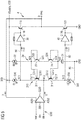
- FIG. 5 shows an improved embodiment of an LDO 4 having sourcing and sinking capabilities.
- the LDO 4 shown in Figure 5 comprises an output node O to provide a regulated output voltage Vreg.
- An output current branch 100 is coupled to the output node O between a supply line Vsupply to provide a supply voltage VDD and a reference potential.
- the output current branch 100 comprises an output driver 110 that may be configured as an output transistor and an output driver 120 that may be configured as an output transistor. Both of the output drivers are configured to be operated in a first and a second operating state. When operated in the first operating state, the respective conductivity of the output driver 110 and the output driver 120 is higher than in the second operating state of the drivers.
- the first operating state of the output drivers 110 and 120 may be a conductive state of the transistors and the second operating state may be a non-conductive state of the output drivers.
- the LDO 4 further comprises an input amplifier stage 200 having an input side 1200 to apply an input signal Vin being a differential signal of the reference signal Vref and the feedback signal Vfb that is derived from the regulated output signal Vreg.
- the input amplifier stage 200 has an output side 0200 to provide a control current I1 to control the operating state of the output driver 110 and the output driver 120.
- the input amplifier stage 200 generates the control current I1 in dependence on the input signal Vin.
- the LDO 4 further comprises a current generator unit 300 to provide a control current 12 to operate the output driver 110 in the second operating state, for example a state of low conductivity or a non-conductive state, and to provide a control current 13 to operate the output driver 120 in the second operating state, for example a state of low conductivity or a non-conductive state, when the output current I1 at the output side 0200 of the input amplifier stage 200 is below a threshold level or is a zero signal, i.e. a signal having a zero level.
- the current generator unit 300 generates the control current 12 and the control current 13 to operate the output drivers 110 and 120 in the low conductive or non-conductive state, when the LDO regulator is operated in the unloaded state or the control current I1 is zero or very small.
- the current generator unit 300 comprises a current generator 310.
- the output side 0200 of the input amplifier stage 200 is coupled to the current generator 310.
- the current generator 310 may be configured as a floating current generator.
- the current generator unit 300 further comprises a current generator 320 and a current generator 330 being coupled in series with the current generator 310 in a first current branch 10.
- the first current branch 10 is arranged between the supply line Vsupply to provide the supply potential VDD and a reference potential.
- the current generator 310 comprises a first transistor 311 and a second transistor 312.
- the first and the second transistors 311 and 312 of the first current generator 310 are of a different type of conductivity.
- the first transistor 311 may be configured as an NMOS transistor and the second transistor 312 may be configured as a PMOS transistor.
- the first transistor 311 and the second transistor 312 of the current generator 310 are connected in series such that the source node S311 of the first transistor 311 is connected to the source node S312 of the second transistor 312 of the current generator 310.
- the current generator 320 is connected to the drain connection D311 of the first transistor 311 of the current generator 310.
- the current generator 330 is connected to the drain connection D312 of the second transistor 312 of the current generator 310.
- the LDO 4 further comprises a voltage source 21, a current generator 22, a transistor 23 and a transistor 24 being connected in series in a second current branch 20 between the supply line Vsupply and a reference potential.
- the transistors 23 and 24 are configured as transistors of a different type of conductivity.
- the transistor 23 may be configured as an NMOS transistor and the transistor 24 may be configured as a PMOS transistor.
- the positive terminal of the voltage source 21 is coupled to the supply potential and the current generator 22 is connected from a node N22 to ground GND.
- the transistor 23 and the transistor 24 of the second current branch 20 are connected in series such that the source node S23 of the transistor 23 is connected to the source S24 of the transistor 24.
- the current generator 22 is connected to the drain connection D23 of the transistor 23.
- the drain connection D24 of the transistor 24 is connected to the voltage source 21.
- the second current branch 20 is coupled between the supply line Vsupply to provide the supply voltage VDD and a reference potential.
- a control connection G311 of the transistor 311 is connected to a node N21 of the second current branch 20 between the drain connection D23 of the transistor 23 and the current generator 22.
- a control connection G312 of the transistor 312 is connected to a node N22 of the second current branch 20 between the drain connection D24 of the transistor 24 and the voltage source 21.
- the transistors 23 and 311 as well as the transistors 24 and 312 are matched to precisely set the current of the floating generator 310.
- the LDO 4 comprises a first transimpedance amplifier stage 30 being arranged between a control connection G110 of the output driver 110 and a first node N11 of the first current branch 10 between the current generator 310 and the current generator 320.
- the first node N11 of the first current branch 10 is arranged between the current generator 320 and the drain connection D311 of the transistor 311.
- the LDO 4 further comprises a second transimpedance amplifier stage 40 being arranged between a control connection G120 of the output driver 120 and a second node N12 of the first current branch 10 between the current generator 310 and the current generator 330.
- the second node N12 of the first current branch 10 is arranged between the drain connection D312 of the transistor 312 of the current generator 310 and the current generator 330.
- the input amplifier stage 200 comprises at the output side 0200 a first output connection A201 to provide/receive the control current I1.
- the output connection A201 of the input amplifier stage 200 is coupled to the output node O of the LDO 4.
- the input amplifier stage 200 is configured to provide the control current I1 at the output connection A201, when the LDO is operated in the sourcing operation mode.
- the input amplifier stage 200 is configured to receive the control current I1 at the output connection A201, when the LDO 4 is operated in the sinking operation mode.
- the input amplifier stage 200 further comprises at the output side 0200 an output connection A202 to provide/receive the control current I1.
- the output connection A202 of the input amplifier stage 200 is connected to a third node N13 of the first current branch 10 between the source connection S311 of the transistor 311 and the source connection S312 of the transistor 312.
- the input amplifier stage 200 is configured to provide the control current I1 at the output connection A202, when the LDO 4 is operated in the sourcing operation mode.
- the input amplifier stage 200 is further configured to receive the control current I1 at the output connection A202, when the LDO 4 is operated in the sinking operation mode.
- the output driver 110 is operated in the first operating state, i.e. in the operating state in which the output driver 110 has a high conductivity, and the output driver 120 is operated in the second operating state, in which the output driver 120 has a low conductivity or is in the non-conductive state, when the control current I1 provided at the output connection A202 of the input amplifier stage 200 enters the current generator 310.
- the output driver 110 is operated in the second operating state in which the output driver 110 has a low conductivity or is operated in the non-conductive state, and the output driver 120 is operated in the first operating state, in which the output driver 120 has a high conductivity, when the control current I1 received at the output connection A202 of the input amplifier stage 200 exits the current generator 310.
- the input amplifier stage 200 can be any kind of differential pair that generates a control current I1 under an input signal Vin. According to a possible embodiment, the input amplifier stage can be configured as shown in Figure 4 , where only two matched paths for the control current I1 are needed.
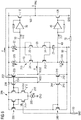
- FIG. 6 shows the LDO 4 with an embodiment of the input amplifier stage 200 in greater detail.
- the input amplifier stage 200 comprises an amplifier stage 210 that is connected to a current source 220.
- the amplifier stage 210 may be configured as an NMOS stage comprising a transistor 211 to receive a feedback signal/voltage Vfb derived from the regulated output signal/voltage Vreg and a transistor 212 to apply a reference signal/voltage Vref.
- the feedback voltage Vfb received at a control terminal of transistor 211 is derived from the regulated output voltage Vreg by means of a feedback net comprising a resistor divider of the resistors 70 and 80.
- the input amplifier stage 200 further comprises PMOS mirror stages 230 and NMOS mirror stages 240.
- the control current I1 provided at the output connection A201 of the input amplifier stage is delivered at the connection between a transistor 234, for example a PMOS transistor, of a first PMOS mirror stage 231, and a transistor 244, for example an NMOS transistor, of a first NMOS mirror stage 241.
- the output connection A202 of the input amplifier stage 200 to provide/receive the control current I1 is located at a connection between a transistor 235, for example a PMOS transistor, of a second PMOS mirror stage 232 and a transistor 245, for example an NMOS transistor, of a second NMOS mirror stage 242.
- a transistor 235 for example a PMOS transistor, of a second PMOS mirror stage 232
- a transistor 245 for example an NMOS transistor, of a second NMOS mirror stage 242.
- the LDO regulator 4 shown in Figures 5 and 6 is configured as a class AB LDO.
- the input amplifier stage 200 can comprise either a P-MOS or N-MOS differential pair and may be even a folded solution.
- a very low impedance set by the transconductance of the transimpedance amplifier stages 30 and 40 drives the large gates of the output transistors 110 and 120.
- the shared signal I1 to drive both pullup and pulldown sections comes as a current mode one, hence no high impedance nodes are present in the loop: Miller compensation is not required and the associated constraints about a load cap and current vanish.
- the transimpedance stages 30 and 40 offer a minimum number of high order poles to ensure excellent phase margin to the structure. In this way, the regulated output might play the role of the dominant pole.
- a current which is matched to the one generated by the input pair closes the loop in this operating condition with minimal drive capability.
- the LDO stability is enforced by exploiting the benefits of the transimpedance amplifier stages 30 and 40 in both senses of the load current.
- the input amplifier stage 200 is a transconductance stage having two output connections A201, A202 only instead of three output connections, as shown for the embodiment of the LDO 3 of Figure 3 .
- control current 13 provided by the current generator 330 it is possible to set the control current 13 provided by the current generator 330 equal to Ia - ⁇ , i.e. equal to the control current 12 provided by the current generator 320.
- the transistors 311 and 23 are a matched pair as well as the transistors 312 and 24. In this way they force a current Ia in the absence of any contribution of the control current I1. As soon as the parameter ⁇ is set to ⁇ > 0, a residual current ⁇ * Ia is injected in both the transimpedance stages 30 and 40 to turn off the output drivers 110 and 120.
- the floating generator acts as a control current splitter as well. Assuming that the same impedance is seen at the source connections of the transistors 311 and 312, the control current I1 provided at the output connection A202 of the input amplifier stage 200 is split half in the upper LDO branch 50, i.e. to the control connection of the output driver 110 and half in the lower LDO branch 60, i.e. to the control connection of the output driver 120.
- the control current I1 is entering the current generator 310, it would tend to subtract current in the LDO lower branch 60 to the control connection of the output driver 120 and increase current in the LDO upper branch 50 to the control connection of the output driver 110.
- the LDO 4 is operated in the sourcing operating state in which the output driver 110 is operated in the conductive state and the output driver 120 is operated in a low-conductive/non-conductive state.
- the control current I1 is exiting the current generator 310, it would tend to increase the current in the lower LDO branch 60 to the control connection of the output driver 120 and subtract current in the upper LDO branch 50 to the control connection of the output driver 110.
- the LDO 4 is operated in the sinking operation mode in which the output driver 110 is operated in a low conductive state/non-conductive state and the output driver 120 is operated in a high conductive state.
- the implementation of the current splitter makes any offset internal to the input amplifier stage 200 ineffective to crowbar generation.
- This is an advantage in comparison to the embodiment of the LDO 3 shown in Figure 3 with the input amplifier stage 200 shown in Figure 4 , where the control current I1 for the pull-up device 110 and the pull-down device 120 are obtained via replica mirrors.
- the transistors in the P-MOS mirror stages and the N-MOS mirror stages might generate DC contributions forcing conduction in both of the driver sections 110 and 120.
- the current generators 320 and 330 do not belong to the signal paths 50, 60 and even if they are very large signal speed is not significantly affected for extreme matching characteristic.
- the impedance at the source connections of the transistors 311 and 312 is one of the lowest in the loop as given by the parallel connection of two transconductances, unlike the mirrors in Figure 4 . Hence, it can be fast enough even if highly loaded by a large parasitic.
Landscapes
- Engineering & Computer Science (AREA)
- Physics & Mathematics (AREA)
- Electromagnetism (AREA)
- General Physics & Mathematics (AREA)
- Radar, Positioning & Navigation (AREA)
- Automation & Control Theory (AREA)
- Amplifiers (AREA)
- Continuous-Control Power Sources That Use Transistors (AREA)
Abstract
Description
- The disclosure relates to a low-dropout regulator having sourcing and sinking capabilities.
- A low-dropout regulator (LDO) is a DC linear voltage regulator that can regulate the output voltage even when the supply voltage is very close to the output voltage. The LDO provides a regulated output voltage at an output node that may be used to supply a load. LDOs are traditionally unidirectional power supplies, i.e. they usually source a current, if the LDO for example replaces a battery.
- The design of LDOs is a challenging task in most cases because of stability concerns. They are intrinsically associated with a device that must source a large current into a big load capacitor. To ensure the required drive capability for an output driver/transistor of the LDO, a large swing is needed at its gate. This automatically implies the presence of a (at least moderately) large impedance node. In addition, the parasitic at the gate of the output transistor is large. Thus, there are possibilities for a low frequency cut-off pole.
- At the same time, the output node of an LDO, loaded by a capacitor which might be as large as possible to ensure a precise regulated voltage, fits well into the role of a dominating pole in the regulation loop. This means that the total phase margin of the circuit structure is expected to be quite poor.
- It is evident that it could be quite complicated to ensure that the LDO is endowed with a bidirectional current capability, i.e. not only the usual sourcing one but also a sinking capability. In fact, the circuitry to correlate the drive at a pull-up device of the LDO to a pull-down device of the LDO would unavoidably introduce other poles and other large parasitics because of the large size of the sinking element.
- It is obvious that as soon as the output branch of an LDO is made by a series connection of two large devices, the need to keep their bias current under control is absolutely mandatory. Any offset or mismatching, even in a properly designed architecture, would make this value unacceptably high because a key feature of an LDO is to dissipate as little power as possible if unloaded.
- It is desired to provide a low-dropout regulator having sourcing and sinking capabilities, wherein the LDO has low power consumption in the sourcing and sinking operation mode as well as in the unloaded state.
- A low-dropout regulator having sourcing and sinking capabilities, wherein the regulator dissipates as little power as possible is specified in claim 1.
- The low-dropout regulator comprises an output node to provide a regulated output voltage. The LDO further comprises an output current branch coupled to the output node, the output current branch comprising a first output driver and a second output driver. The first and the second output drivers are configured to be operated in a first and a second operating state. The respective conductivity of the first and the second output drivers is higher in the first operating state than in the second operating state.
- The LDO further comprises an input amplifier stage having an input side to apply an input signal and an output side to provide a first control current to control the operating state of the first and the second output drivers. The input amplifier stage generates the first control current in dependence on the input signal. The LDO comprises a current generator unit to provide a second control current to operate the first output driver in the second operating state and to provide a third control current to operate the second output driver in the second operating state, when the first control current at the output side of the input amplifier stage is below a threshold level.
- The structure of a traditional LDO just having a sourcing capability is doubled so that the output branch of the LDO comprises a first and an additional second output driver. The LDO has sourcing and sinking capabilities by providing the first and a second output drivers in the output current branch. In dependence on operating the LDO in the sourcing or sinking operation mode, only one of the two output drivers is operated in a high conductive state, whereas the other one of the two output drivers is operated with lower conductivity or even with no conductivity. That means that the LDO is configured as a fully class AB approach unlike usual LDO solutions.
- Furthermore, the current generator unit allows to operate both of the first and second output drivers in the output current branch with low or even no conductivity, when the input signal applied to the input amplifier stage and the first control current has a low level or the output node of the LDO is unloaded. Only under a large signal condition of the input signal at the input side of the input amplifier stage is one of the output drivers of the output current branch turned into the conductive state, while the other of the first and second output drivers is turned in the low-conductive or non-conductive state. Since in any case one or both of the output drivers are turned into the low-/non-conductive state, the LDO has a low power consumption. The quiescent current is made minimal even in the presence of large mismatching.
-
-
Figure 1 shows an embodiment of a transimpedance-based regulator having sourcing capability. -
Figure 2 illustrates a conceptual implementation of an LDO having sourcing and sinking capabilities. -
Figure 3 shows an embodiment of an LDO having sourcing and sinking capabilities and a low power consumption by minimizing crowbar. -
Figure 4 shows an embodiment of an input amplifier stage of an LDO. -
Figure 5 shows another embodiment of an LDO having sourcing and sinking capabilities. -
Figure 6 shows an embodiment of an LDO having sourcing and sinking capabilities with a feedback net to provide a feedback path from the output node of the LDO to the input amplifier stage. -
Figure 1 shows a transimpedance-based architecture 1 of an LDO comprising an outputcurrent branch 100 including anoutput driver 110 that is arranged between a supply line Vsupply and an output node O of the LDO to provide a regulated output voltage Vreg. Theoutput driver 110 may be configured as an output transistor. The output node O is fed back by a feedbackpath comprising resistors input side 1200 of aninput amplifier stage 200. Theinput amplifier stage 200 has a first input node E200a to apply a reference signal Vref and a second input node E200b to apply the fed back signal Vfb derived from the regulated output voltage Vreg. - An
output side 0200 of theinput amplifier stage 200 is coupled to atransimpedance amplifier stage 30 that is arranged between a control connection of theoutput driver 110 and theoutput side 0200 of theinput amplifier stage 200. Thetransimpedance amplifier 30 comprises a transistor 33, acurrent source 34 and aresistor 35. The transistor 33 and thecurrent source 34 are coupled in series between the supply line Vsupply and a reference potential. Theresistor 35 is arranged between the drain connection of the transistor 33 and theoutput side 0200 of theinput amplifier stage 200. - The
output driver 110 may be configured as a power transistor that is driven with a low impedance given by the transconductance of the transistor 33 for a fast drive of its parasitic. Thelarge resistor 35 allows sufficient gain without cutting the large capacitance at the output transistor gate. This arrangement allows the dominant pole at the output node with safe gain and phase margin values. Due to the large value for the transconductance of the transistor 33, the second loop pole can be shifted at a very high frequency and the dominant pole is at the output node. Hence an output capacitor can be increased without limitation to make the regulated output voltage as precise as possible against load current fast variations. - Virtual ground of the
transimpedance stage 30 is set to the gate-source voltage of theoutput transistor 110 for a given current. This determines the load current value that gives the zero offset condition at the LDO input and sets the proper control in the output stage current. - In the implementation of the LDO shown in
Figure 1 , theoutput transistor 110 and the transistor 33 of thetransimpedance amplifier stage 30 are matched devices so that theoutput driver 110 will tend to drive n-times the current across theresistor 35 as soon as the drop across theresistor 35 is zero. As the output voltage Vreg is pulled down by the load only, the current across theoutput driver 110 remains equal to a load current regardless of any offset between theoutput transistor 110 and the transistor 33 of thetransimpedance amplifier stage 30 and any offset current from theinput amplifier stage 200 to theresistor 35. - The advantages of the circuit structure shown in
Figure 1 can be exploited by implementing a complementary LDO having both sourcing and sinking capabilities, according to the implementation shown inFigure 2 . -
Figure 2 shows a conceptual implementation of an LDO. The circuit structure of the LDO illustrated inFigure 1 is doubled so that the LDO inFigure 2 comprises an LDO up-portion 2a and an LDO down-portion 2b. The LDO up-portion 2a comprises afirst output driver 110 arranged between a supply line Vsupply and an output node O. Theoutput driver 110 may be configured as an output transistor. The LDO up-portion further comprises aninput amplifier stage 200a, and atransimpedance amplifier stage 30 comprising atransimpedance amplifier 31 and aresistor 32 that couples the output of thetransimpedance amplifier 31 back to the input connection of thetransimpedance amplifier 31. Thetransimpedance amplifier stage 30 is coupled between a control connection G110 of theoutput driver 110 and the output side of theinput amplifier stage 200a. A reference signal Vref is applied at an input connection, for example a non-inverting input connection, of theinput amplifier stage 200a. A second connection, for example an inverting connection, of theinput amplifier stage 200a is connected to the output node O of the LDO amplifier. - The LDO down-
portion 2b comprises anoutput driver 120 arranged between the output node O and the reference potential. Theoutput driver 120 may be configured as an output transistor. The LDO down-portion 2b further comprises aninput amplifier stage 200b and atransimpedance amplifier stage 40. Thetransimpedance amplifier stage 40 is arranged between a control connection G120 of theoutput driver 120 and an output side of theinput amplifier stage 200b. Thetransimpedance stage 40 comprises atransimpedance amplifier 41 and aresistor 42 that couples the output of thetransimpedance amplifier 41 back to the input connection of thetransimpedance amplifier 41. The reference signal Vref is applied to a first input connection, for example a non-inverting input connection, of theinput amplifier stage 200b. The output node O is connected to a second input connection, for example an inverting input connection, of theinput amplifier stage 200b. - The
output drivers output branch 100 of the LDO regulator between a supply line Vsupply and a reference potential. The output drivers are configured as transistors of a different type of conductivity. Theoutput driver 110 may be configured, for example, as a PMOS transistor, and theoutput driver 120 may be configured, for example, as an NMOS transistor. Thetransimpedance output driver 120, for example the NMOS transistor, asks for lower overdrive than theoutput driver 110, for example the PMOS counterpart. -
Figure 2 shows shows a unity gain for the LDO stage, as it is only conceptual. Of course a feedback net can be adopted to make the regulated output voltage Vreg higher than the value of the reference voltage Vref. In this case, one resistor goes from the output side O of the LDO to the negative inputs (the same node is shared by both) of theamplifiers - The implementation of the LDO amplifier shown in
Figure 2 has some significant drawbacks in practical use. The offset in one stage, for example the LDO up-portion 2a or the LDO down-portion 2b, may cause large conduction in the associated power transistor. Assuming that the offset of theLDO portions current branch 100 is no longer fixed by the load one only and unacceptably large value of power consumption might come even for light load values. -
Figure 3 shows an improved embodiment of anLDO 3 having sourcing and sinking capabilities, wherein the crowbar issue, i.e. the contemporary conduction of the two output drivers/transistors LDO branches - According to the embodiment of the
LDO 3 ofFigure 3 , the LDO comprises an output node O to provide a regulated output voltage Vreg, wherein the output node O is arranged in an outputcurrent branch 100 of the LDO. The outputcurrent branch 100 comprises afirst output driver 110 that may be configured as an output transistor and asecond output driver 120 that may be configured as an output transistor. Theoutput driver 110 and theoutput driver 120 are configured of a different type of conductivity. Theoutput driver 110 may be configured as a PMOS transistor, and theoutput driver 120 may be configured as an NMOS transistor. - The first and the
second output drivers output driver 110 and theoutput driver 120 is higher in the first operating state than in the second operating state of the transistors. The first operating state may be the conductive state of the output drivers and the second operating state may be the non-conductive state. - The
LDO 3 comprises aninput amplifier stage 200 having aninput side 1200 to apply an input signal Vin and anoutput side 0200 to provide a first control current I1 to control the operating state of theoutput drivers input amplifier stage 200 generates the first control current I1 in dependence on the input signal Vin being a differential signal derived from the reference signal Vref and the fed back signal Vfb. - The
LDO 3 comprises acurrent generator unit 300 to provide a second control current 12 to operate theoutput driver 110 in the second operating state, for example the non-conductive operating state, and to provide a third control current 13 to operate theoutput driver 120 in the second operating state, for example the low-conductive/non-conductive operating state, when the first control current I1 at theoutput side 0200 of theinput amplifier stage 200 is below a threshold level, for example, is a zero signal. - The
LDO 3 comprises a firsttransimpedance amplifier stage 30 being connected to a control connection G110 of theoutput driver 110. TheLDO 3 further comprises a secondtransimpedance amplifier stage 40 being connected to a control connection G120 of theoutput driver 120. Each of the transimpedance amplifier stages 30 and 40 comprises atransimpedance amplifier transimpedance respective transimpedance amplifier - The
input amplifier stage 200 has three output connections at itsoutput side 0200. Theinput amplifier stage 200 comprises a first output connection A201 to provide/receive the first control current I1. The first output connection A201 of theinput amplifier 200 is connected to the output node O of theLDO 3. Theinput amplifier stage 200 comprises at the output side 0200 a second output connection A202 and a third output connection A203 to provide/receive the first control current I1. The second output connection A202 of theinput amplifier stage 200 is connected to the firsttransimpedance amplifier stage 30. The third output connection A203 of theinput amplifier stage 200 is connected to the secondtransimpedance amplifier stage 40. The three current branches at theoutput side 0200 must match precisely, but it is not necessary that they have the same nominal value. They can be different multiples from a unit value, this being especially true for the branch directly feeding the LDO output O. - The
current generator unit 300 comprises a firstcurrent generator 340 and a secondcurrent generator 350. The firstcurrent generator 340 is connected to the firsttransimpedance amplifier stage 30 to provide the second control current 12 that causes to operate theoutput driver 110 in the second operating state, for example the non-conductive operating state. The secondcurrent generator 350 is connected to the secondtransimpedance amplifier stage 40 to provide the third control current 13 that causes to operate theoutput driver 120 in the second operating state, for example the non-conductive operating state. - The
LDO 3 ofFigure 3 is configured as a class AB regulator. The class AB property is ensured by the control current I1 being injected into the twotransimpedance stages transimpedance stage 30 and the pull-down side represented by thetransimpedance stage 40. - In the case of a positive value of the control current I1, i.e. if the LDO is operated in the sourcing operation mode and the control current I1 is injected by the
input amplifier stage 200 in the transimpedance stages 30 and 40, theoutput driver 110 is turned on, i.e. switched in a state of high conductivity, so that the current flowing through theoutput driver 110 is increased. On the other hand, the control current I1 injected in thetransimpedance stage 40 has the effect that theoutput driver 120 moves to an even deeper turn-off status, i.e. to a state of low conductivity or no conductivity. - For a negative value of the control current I1, i.e. if the
LDO 3 is operated in the sinking operation mode and the control current I1 exits thecurrent generator unit 300 and is injected ininput amplifier stage 200, theoutput driver 110 is turned off or turned in a low-conductive state/non-conductive state, while theoutput driver 120 is turned on or turned in a high conductive state. - When the input voltage of the
input amplifier stage 200 is very small, the control current 12 provided by thecurrent generator 340 turns theoutput driver 110 off, i.e. in an operation state of low conductivity or the non-conductive operation state, and the control current 13 provided by thecurrent generator 350 turns theoutput driver 120 off, i.e. in an operation state of low conductivity or the non-conductive operation state. That means that in the unloaded configuration both of theoutput drivers control currents - As for both branches, i.e. the pull-up and pull-down branch, the original structure shown in
Figure 1 is preserved. The stability concerns are unaltered, and in particular, a Miller compensation is not required. The output node A201 directly drives the output node O and ensures the loop closure when the control current I1 is zero or very small (I1 < 12 or I1 < 13). The LDO may be embodied such that thecontrol currents Figure 3 in which the control current 12 and 13 turn off theoutput drivers transimpedance stages Figure 1 to achieve the same result. -
Figure 4 shows a possible embodiment for theinput amplifier stage 200 of theLDO 3 ofFigure 3 . The embodiment of theinput amplifier stage 200 shown inFigure 4 is configured to provide the three replicas of the three control currents I1 to drive the twotransimpedance stages input amplifier stage 200 comprises anamplifier stage 210 that may be configured as an NMOS amplifier stage or a PMOS amplifier stage, depending on the available dynamic range. Theamplifier stage 210 comprises atransistor 211 to apply a feedback voltage Vfb derived from the regulated output voltage Vreg at the output node O and atransistor 212 to apply the reference voltage Vref. Theamplifier stage 210 is connected to acurrent source 220. - The
input amplifier stage 200 further comprises PMOS mirror stages 230 and NMOS mirror stages 240. The control current I1 provided at the output connection A201 is delivered at the connection between aPMOS transistor 234 of a firstPMOS mirror stage 231 and anNMOS transistor 244 of a firstNMOS mirror stage 241. The control current I1 provided at the output connection A202 of theinput amplifier stage 200 is delivered at the connection between aPMOS transistor 235 of a secondPMOS mirror stage 232 and anNMOS transistor 245 of a secondNMOS mirror stage 242. The control current I1 provided at the output connection A203 of theinput amplifier stage 200 is delivered at the connection between aPMOS transistor 236 of a thirdPMOS mirror stage 233 and anNMOS transistor 246 of a thirdNMOS mirror stage 243. - As described above, the embodiment of the
input amplifier stage 200 shown inFigure 4 comprises a plurality of mirrors. The circuit configuration ofFigure 4 may be critical in case of an offset between the mirrors. The offset can cause the control current I1 being injected in thetransimpedance stage 30 and thetransimpedance stage 40, when the LDO ofFigure 3 is operated in the unloaded operation state. In this case the control current I1 may be so large so that the control current 12 and the control current 13 may be compensated. As a consequence, theoutput drivers output drivers -
Figure 5 shows an improved embodiment of an LDO 4 having sourcing and sinking capabilities. The LDO 4 shown inFigure 5 comprises an output node O to provide a regulated output voltage Vreg. An outputcurrent branch 100 is coupled to the output node O between a supply line Vsupply to provide a supply voltage VDD and a reference potential. The outputcurrent branch 100 comprises anoutput driver 110 that may be configured as an output transistor and anoutput driver 120 that may be configured as an output transistor. Both of the output drivers are configured to be operated in a first and a second operating state. When operated in the first operating state, the respective conductivity of theoutput driver 110 and theoutput driver 120 is higher than in the second operating state of the drivers. According to a possible embodiment, the first operating state of theoutput drivers - The LDO 4 further comprises an
input amplifier stage 200 having aninput side 1200 to apply an input signal Vin being a differential signal of the reference signal Vref and the feedback signal Vfb that is derived from the regulated output signal Vreg. Theinput amplifier stage 200 has anoutput side 0200 to provide a control current I1 to control the operating state of theoutput driver 110 and theoutput driver 120. Theinput amplifier stage 200 generates the control current I1 in dependence on the input signal Vin. - The LDO 4 further comprises a
current generator unit 300 to provide a control current 12 to operate theoutput driver 110 in the second operating state, for example a state of low conductivity or a non-conductive state, and to provide a control current 13 to operate theoutput driver 120 in the second operating state, for example a state of low conductivity or a non-conductive state, when the output current I1 at theoutput side 0200 of theinput amplifier stage 200 is below a threshold level or is a zero signal, i.e. a signal having a zero level. In particular, thecurrent generator unit 300 generates the control current 12 and the control current 13 to operate theoutput drivers - The
current generator unit 300 comprises acurrent generator 310. Theoutput side 0200 of theinput amplifier stage 200 is coupled to thecurrent generator 310. Thecurrent generator 310 may be configured as a floating current generator. Thecurrent generator unit 300 further comprises acurrent generator 320 and a current generator 330 being coupled in series with thecurrent generator 310 in a firstcurrent branch 10. The firstcurrent branch 10 is arranged between the supply line Vsupply to provide the supply potential VDD and a reference potential. Thecurrent generator 310 comprises afirst transistor 311 and asecond transistor 312. The first and thesecond transistors current generator 310 are of a different type of conductivity. Thefirst transistor 311 may be configured as an NMOS transistor and thesecond transistor 312 may be configured as a PMOS transistor. Thefirst transistor 311 and thesecond transistor 312 of thecurrent generator 310 are connected in series such that the source node S311 of thefirst transistor 311 is connected to the source node S312 of thesecond transistor 312 of thecurrent generator 310. Thecurrent generator 320 is connected to the drain connection D311 of thefirst transistor 311 of thecurrent generator 310. The current generator 330 is connected to the drain connection D312 of thesecond transistor 312 of thecurrent generator 310. - The LDO 4 further comprises a
voltage source 21, a current generator 22, atransistor 23 and atransistor 24 being connected in series in a secondcurrent branch 20 between the supply line Vsupply and a reference potential. Thetransistors transistor 23 may be configured as an NMOS transistor and thetransistor 24 may be configured as a PMOS transistor. According to another possible embodiment for the second current branch, the positive terminal of thevoltage source 21 is coupled to the supply potential and the current generator 22 is connected from a node N22 to ground GND. - The
transistor 23 and thetransistor 24 of the secondcurrent branch 20 are connected in series such that the source node S23 of thetransistor 23 is connected to the source S24 of thetransistor 24. The current generator 22 is connected to the drain connection D23 of thetransistor 23. The drain connection D24 of thetransistor 24 is connected to thevoltage source 21. The secondcurrent branch 20 is coupled between the supply line Vsupply to provide the supply voltage VDD and a reference potential. - A control connection G311 of the
transistor 311 is connected to a node N21 of the secondcurrent branch 20 between the drain connection D23 of thetransistor 23 and the current generator 22. A control connection G312 of thetransistor 312 is connected to a node N22 of the secondcurrent branch 20 between the drain connection D24 of thetransistor 24 and thevoltage source 21. Thetransistors transistors generator 310. - The LDO 4 comprises a first
transimpedance amplifier stage 30 being arranged between a control connection G110 of theoutput driver 110 and a first node N11 of the firstcurrent branch 10 between thecurrent generator 310 and thecurrent generator 320. In particular, the first node N11 of the firstcurrent branch 10 is arranged between thecurrent generator 320 and the drain connection D311 of thetransistor 311. - The LDO 4 further comprises a second
transimpedance amplifier stage 40 being arranged between a control connection G120 of theoutput driver 120 and a second node N12 of the firstcurrent branch 10 between thecurrent generator 310 and the current generator 330. In particular, the second node N12 of the firstcurrent branch 10 is arranged between the drain connection D312 of thetransistor 312 of thecurrent generator 310 and the current generator 330. - The
input amplifier stage 200 comprises at the output side 0200 a first output connection A201 to provide/receive the control current I1. The output connection A201 of theinput amplifier stage 200 is coupled to the output node O of the LDO 4. Theinput amplifier stage 200 is configured to provide the control current I1 at the output connection A201, when the LDO is operated in the sourcing operation mode. Theinput amplifier stage 200 is configured to receive the control current I1 at the output connection A201, when the LDO 4 is operated in the sinking operation mode. - The
input amplifier stage 200 further comprises at theoutput side 0200 an output connection A202 to provide/receive the control current I1. The output connection A202 of theinput amplifier stage 200 is connected to a third node N13 of the firstcurrent branch 10 between the source connection S311 of thetransistor 311 and the source connection S312 of thetransistor 312. Theinput amplifier stage 200 is configured to provide the control current I1 at the output connection A202, when the LDO 4 is operated in the sourcing operation mode. Theinput amplifier stage 200 is further configured to receive the control current I1 at the output connection A202, when the LDO 4 is operated in the sinking operation mode. - The
output driver 110 is operated in the first operating state, i.e. in the operating state in which theoutput driver 110 has a high conductivity, and theoutput driver 120 is operated in the second operating state, in which theoutput driver 120 has a low conductivity or is in the non-conductive state, when the control current I1 provided at the output connection A202 of theinput amplifier stage 200 enters thecurrent generator 310. - The
output driver 110 is operated in the second operating state in which theoutput driver 110 has a low conductivity or is operated in the non-conductive state, and theoutput driver 120 is operated in the first operating state, in which theoutput driver 120 has a high conductivity, when the control current I1 received at the output connection A202 of theinput amplifier stage 200 exits thecurrent generator 310. - The
input amplifier stage 200 can be any kind of differential pair that generates a control current I1 under an input signal Vin. According to a possible embodiment, the input amplifier stage can be configured as shown inFigure 4 , where only two matched paths for the control current I1 are needed. -
Figure 6 shows the LDO 4 with an embodiment of theinput amplifier stage 200 in greater detail. Theinput amplifier stage 200 comprises anamplifier stage 210 that is connected to acurrent source 220. Theamplifier stage 210 may be configured as an NMOS stage comprising atransistor 211 to receive a feedback signal/voltage Vfb derived from the regulated output signal/voltage Vreg and atransistor 212 to apply a reference signal/voltage Vref. The feedback voltage Vfb received at a control terminal oftransistor 211 is derived from the regulated output voltage Vreg by means of a feedback net comprising a resistor divider of theresistors - The
input amplifier stage 200 further comprises PMOS mirror stages 230 and NMOS mirror stages 240. The control current I1 provided at the output connection A201 of the input amplifier stage is delivered at the connection between atransistor 234, for example a PMOS transistor, of a firstPMOS mirror stage 231, and atransistor 244, for example an NMOS transistor, of a firstNMOS mirror stage 241. The output connection A202 of theinput amplifier stage 200 to provide/receive the control current I1 is located at a connection between atransistor 235, for example a PMOS transistor, of a secondPMOS mirror stage 232 and atransistor 245, for example an NMOS transistor, of a secondNMOS mirror stage 242. Regarding the other components of the LDO regulator 4 shown inFigure 6 , reference is made toFigure 5 . - The LDO regulator 4 shown in
Figures 5 and6 is configured as a class AB LDO. Depending on the input range, theinput amplifier stage 200 can comprise either a P-MOS or N-MOS differential pair and may be even a folded solution. - A very low impedance set by the transconductance of the transimpedance amplifier stages 30 and 40, drives the large gates of the
output transistors - A small offset current, injected in the transimpedance stages 30 and 40 by the floating generator represented by the
transistors power devices input amplifier stage 200. A current which is matched to the one generated by the input pair closes the loop in this operating condition with minimal drive capability. The LDO stability is enforced by exploiting the benefits of the transimpedance amplifier stages 30 and 40 in both senses of the load current. - According to the embodiment of the LDO 4 shown in
Figures 5 and6 , theinput amplifier stage 200 is a transconductance stage having two output connections A201, A202 only instead of three output connections, as shown for the embodiment of theLDO 3 ofFigure 3 . The offset in the transimpedance stages 30 and 40 is obtained via a series combination of a floating generator, i.e. thetransistors current generators 320 and 330. Assuming the current generator 22 provides a current 10 = Ia, thecurrent generator 320 provide the control current 12 = Ia - ε and the current generator 330 provides the control current 13 = Ib. Of course, to have a symmetrical offset for equal resistors in the transimpedance stage, it is possible to set the control current 13 provided by the current generator 330 equal to Ia - ε, i.e. equal to the control current 12 provided by thecurrent generator 320. - The
transistors transistors output drivers - At the same time, the floating generator acts as a control current splitter as well. Assuming that the same impedance is seen at the source connections of the
transistors input amplifier stage 200 is split half in theupper LDO branch 50, i.e. to the control connection of theoutput driver 110 and half in thelower LDO branch 60, i.e. to the control connection of theoutput driver 120. - If the control current I1 is entering the
current generator 310, it would tend to subtract current in the LDOlower branch 60 to the control connection of theoutput driver 120 and increase current in the LDOupper branch 50 to the control connection of theoutput driver 110. In this case the LDO 4 is operated in the sourcing operating state in which theoutput driver 110 is operated in the conductive state and theoutput driver 120 is operated in a low-conductive/non-conductive state. On the other hand, if the control current I1 is exiting thecurrent generator 310, it would tend to increase the current in thelower LDO branch 60 to the control connection of theoutput driver 120 and subtract current in theupper LDO branch 50 to the control connection of theoutput driver 110. In this case the LDO 4 is operated in the sinking operation mode in which theoutput driver 110 is operated in a low conductive state/non-conductive state and theoutput driver 120 is operated in a high conductive state. - In this way, the implementation of the current splitter makes any offset internal to the
input amplifier stage 200 ineffective to crowbar generation. This is an advantage in comparison to the embodiment of theLDO 3 shown inFigure 3 with theinput amplifier stage 200 shown inFigure 4 , where the control current I1 for the pull-updevice 110 and the pull-downdevice 120 are obtained via replica mirrors. According to the embodiment of theLDO 3 shown inFigures 3 and 4 , the transistors in the P-MOS mirror stages and the N-MOS mirror stages might generate DC contributions forcing conduction in both of thedriver sections - Thus, according to the embodiment of the LDO 4, a large degree of matching is not needed in the mirrors of the
input amplifier stage 200. As a result, smaller and less, i.e. two instead of three, replica current generators that make the overall signal path faster, are obtained. On the other side, it is clear that crowbar minimization asks for the highest degree of matching between the three series current generators of the current splitter, i.e. thecurrent generator - Anyhow, the
current generators 320 and 330 do not belong to thesignal paths transistors Figure 4 . Hence, it can be fast enough even if highly loaded by a large parasitic. -
- 1, 2, 3
- embodiments of LDO regulators
- 10, 20
- current branches of the LDO
- 21
- voltage source
- 22
- current generator
- 23, 24
- transistors
- 30, 40
- transimpedance amplifier stages
- 50, 60
- upper and lower LDO branch
- 70, 80
- resistors
- 100
- output current branch
- 110, 120
- output drivers
- 200
- input amplifier stage
- 210
- amplifier stage
- 220
- current generator
- 230
- PMOS mirrors
- 240
- NMOS mirrors
- 300
- current generator unit
- 310, 320, 330
- current generators
- O
- output node
- I1, I2, I3
- control currents
- Vreg
- regulated output voltage
- Vin
- input signal
- Vref
- reference signal
- Vfb
- feedback signal
Claims (15)
- A low-dropout regulator, comprising:- an output node (O) to provide a regulated output voltage (Vreg),- an output current branch (100) coupled to the output node (O), the output current branch comprising a first output driver (110) and a second output driver (120), wherein the first and the second output driver (110, 120) are configured to be operated in a first and a second operating state, wherein the respective conductivity of the first and the second output driver (110, 120) is higher in the first operating state than in the second operating state,- an input amplifier stage (200) having an input side (1200) to apply an input signal (Vin) and an output side (0200) to provide a first control current (I1) to control the operating state of the first and the second output driver (110, 120), wherein the input amplifier stage (200) generates the first control current (I1) in dependence on the input signal (Vin),- a current generator unit (300) to provide a second control current (12) to operate the first output driver (110) in the second operating state and to provide a third control current (13) to operate the second output driver (120) in the second operating state, when the first control current (I1) at the output side (0200) of the input amplifier stage (200) is below a threshold level.
- The low-dropout regulator of claim 1,- wherein the current generator unit (300) comprises a first current generator (310),- wherein the output side (0200) of the input amplifier stage (200) is coupled to the first current generator (310).
- The low-dropout regulator of claim 2,
wherein the first current generator (310) is configured as a floating current generator. - The low-dropout regulator of claims 2 or 3,- wherein the first output driver (110) is operated in the first operating state and the second output driver (120) is operated in the second operating state, when the first control current (I1) enters the first current generator (310),- wherein the first output driver (110) is operated in the second operating state and the second output driver (120) is operated in the first operating state, when the first control current (I1) exits the first current generator (310).
- The low-dropout regulator of claims 1 to 4, comprising:- a first current branch (10),- wherein the current generator unit (300) comprises a second current generator (320) and a third current generator (330) being coupled in series with the first current generator (310) in the first current branch (10).
- The low-dropout regulator of claims 2 to 5,
wherein the first current generator (310) comprises a first transistor (311) and a second transistor (312) being of a different type of conductivity. - The low-dropout regulator of claim 6,
wherein the first transistor (311) and the second transistor (312) are connected in series such that the source node (S311) of the first transistor (311) is connected to the source node (S312) of the second transistor (312). - The low-dropout regulator of claim 7, comprising:- a second current branch (20),- wherein the second current branch (20) comprises a voltage source (21) and a fourth current generator (22) and third transistor (23) and a fourth transistor (24) being connected in series in the second current branch (20), the third and fourth transistor (23, 24) being of a different type of conductivity.
- The low-dropout regulator of claim 8,
wherein the third transistor (23) and the fourth transistor (24) are connected in series such that the source node (S23) of the third transistor (23) is connected to the source node (S24) of the fourth transistor (24). - The low-dropout regulator of claims 8 or 9,- wherein a control connection (G311) of the first transistor (311) is connected to a first node (N21) of the second current branch (20) between the drain connection (D23) of the third transistor (23) and the fourth current generator (22),- wherein a control connection (G312) of the second transistor (312) is connected to a second node (N22) of the second current branch (20) between the drain connection (D24) of the fourth transistor (24) and the voltage source (21).
- The low-dropout regulator of claims 5 to 10, comprising:- a first transimpedance amplifier stage (30) being arranged between a control connection (G110) of the first output driver (110) and a first node (N11) of the first current branch (10) between the first current generator (310) and the second current generator (320),- a second transimpedance amplifier stage (40) being arranged between a control connection (G120) of the second output driver (120) and a second node (N12) of the first current branch (10) between the first current generator (310) and the third current generator (330).
- The low-dropout regulator of claims 5 to 11,- wherein the input amplifier stage (200) comprises at the output side (0200) a first output connection (A201) to provide/receive the first control current (I1), wherein the first output connection (A201) of the input amplifier stage (200) is coupled to the output node (O) of the low-dropout regulator,- wherein the input amplifier stage (200) comprises at the output side (0200) a second output connection (A202) to provide/receive the first control current (I1), wherein the second output connection (A202) of the input amplifier stage (200) is coupled to a third node (N13) of the first current branch (10) between the source connection (S311) of the first transistor (311) and the source connection (S312) of the second transistor (312).
- The low-dropout regulator of claim 1, comprising:- a first transimpedance amplifier stage (30) being connected to a control connection (G110) of the first output driver (110),- a second transimpedance amplifier stage (40) being connected to a control connection (G120) of the second output driver (120),- wherein the input amplifier stage (200) comprises at the output side (0200) a first output connection (A201) to provide/receive the first control current (I1), wherein the first output connection (A201) of the input amplifier (200) is connected to the output node (O) of the low-dropout regulator,- wherein the input amplifier stage (200) comprises at the output side (0200) a second output connection (A202) and a third output connection (A203) to provide/receive the first control current (I1), wherein the second output connection (A202) of the input amplifier stage (200) is connected to the first transimpedance amplifier stage (30) and the third output connection (A203) of the input amplifier stage (200) is connected to the second transimpedance amplifier stage (40).
- The low-dropout regulator of claim 13,- wherein the current generator unit (300) comprises a first current generator (340) and a second current generator (350),- wherein the first current generator (340) is connected to the first transimpedance amplifier stage (30) to provide a second control current (12) to operate the first output driver (110) in the second operating state,- wherein the second current generator (350) is connected to the second transimpedance amplifier stage (40) to provide a third control current (13) to operate the second output driver (120) in the second operating state.
- The low-dropout regulator of claims 1 to 14,
wherein the first output driver (110) is configured as a transistor of a first type of conductivity and the second output driver (120) is configured as a transistor of a second type of conductivity being different from the first type of conductivity.
Priority Applications (4)
| Application Number | Priority Date | Filing Date | Title |
|---|---|---|---|
| EP17158151.5A EP3367202B1 (en) | 2017-02-27 | 2017-02-27 | Low-dropout regulator having sourcing and sinking capabilities |
| PCT/EP2018/050732 WO2018153565A1 (en) | 2017-02-27 | 2018-01-12 | Low-dropout regulator having sourcing and sinking capabilities |
| CN201880013658.2A CN110325942B (en) | 2017-02-27 | 2018-01-12 | Low dropout regulator with output and input capability |
| US16/485,831 US10691152B2 (en) | 2017-02-27 | 2018-01-12 | Low-dropout regulator having sourcing and sinking capabilities |
Applications Claiming Priority (1)
| Application Number | Priority Date | Filing Date | Title |
|---|---|---|---|
| EP17158151.5A EP3367202B1 (en) | 2017-02-27 | 2017-02-27 | Low-dropout regulator having sourcing and sinking capabilities |
Publications (2)
| Publication Number | Publication Date |
|---|---|
| EP3367202A1 true EP3367202A1 (en) | 2018-08-29 |
| EP3367202B1 EP3367202B1 (en) | 2020-05-27 |
Family
ID=58185417
Family Applications (1)
| Application Number | Title | Priority Date | Filing Date |
|---|---|---|---|
| EP17158151.5A Active EP3367202B1 (en) | 2017-02-27 | 2017-02-27 | Low-dropout regulator having sourcing and sinking capabilities |
Country Status (4)
| Country | Link |
|---|---|
| US (1) | US10691152B2 (en) |
| EP (1) | EP3367202B1 (en) |
| CN (1) | CN110325942B (en) |
| WO (1) | WO2018153565A1 (en) |
Cited By (2)
| Publication number | Priority date | Publication date | Assignee | Title |
|---|---|---|---|---|
| CN113406989A (en) * | 2021-06-18 | 2021-09-17 | 东莞市长工微电子有限公司 | Low dropout linear regulator compensation circuit and low dropout linear regulator |
| CN118051089A (en) * | 2024-04-12 | 2024-05-17 | 北京中天星控科技开发有限公司成都分公司 | A bidirectional current low voltage drop linear regulator |
Families Citing this family (8)
| Publication number | Priority date | Publication date | Assignee | Title |
|---|---|---|---|---|
| EP3379369B1 (en) * | 2017-03-23 | 2021-05-26 | ams AG | Low-dropout regulator having reduced regulated output voltage spikes |
| US11791725B2 (en) | 2020-08-06 | 2023-10-17 | Mediatek Inc. | Voltage regulator with hybrid control for fast transient response |
| US11720128B2 (en) * | 2021-06-29 | 2023-08-08 | Stmicroelectronics S.R.L. | Voltage regulator |
| CN114442717B (en) * | 2022-01-21 | 2023-04-07 | 星宸科技股份有限公司 | Low dropout regulator with bidirectional current regulation |
| TWI811974B (en) * | 2022-01-26 | 2023-08-11 | 大陸商星宸科技股份有限公司 | Low-dropout regulator having bidirectional current adjustment |
| US12332671B2 (en) * | 2023-03-27 | 2025-06-17 | Nanya Technology Corporation | Startup circuit and bandgap circuit |
| CN117519383A (en) * | 2023-11-14 | 2024-02-06 | 江南大学 | Feedforward low-voltage linear voltage stabilizing circuit with symmetrical structure and voltage stabilizing output method |
| CN119105604A (en) * | 2024-09-23 | 2024-12-10 | 浙江大学 | An LDO circuit with both current sourcing and current sinking capabilities |
Citations (6)
| Publication number | Priority date | Publication date | Assignee | Title |
|---|---|---|---|---|
| US20090302683A1 (en) * | 2008-06-04 | 2009-12-10 | Wei-Chung Wu | Multi-Rail Power-Supply System |
| EP2328056A1 (en) * | 2009-11-26 | 2011-06-01 | Dialog Semiconductor GmbH | Low-dropout linear regulator (LDO), method for providing an LDO and method for operating an LDO |
| CN102411394A (en) * | 2011-11-10 | 2012-04-11 | 昌芯(西安)集成电路科技有限责任公司 | Linear voltage stabilizer with low pressure differential and Sink and Source current capabilities |
| US20150340995A1 (en) * | 2014-05-20 | 2015-11-26 | Cambridge Silicon Radio Limited | Current regulated transimpedance amplifiers |
| US20150378377A1 (en) * | 2014-06-26 | 2015-12-31 | Dialog Semiconductor Gmbh | Robust sink / source output stage and control circuit |
| US20160187902A1 (en) * | 2014-12-29 | 2016-06-30 | STMicroelectronics (Shenzhen) R&D Co. Ltd | Two-stage error amplifier with nested-compensation for ldo with sink and source ability |
Family Cites Families (13)
| Publication number | Priority date | Publication date | Assignee | Title |
|---|---|---|---|---|
| US5446412A (en) * | 1994-05-19 | 1995-08-29 | Exar Corporation | Continuously linear pulse amplifier/line driver with large output swing |
| US8054055B2 (en) * | 2005-12-30 | 2011-11-08 | Stmicroelectronics Pvt. Ltd. | Fully integrated on-chip low dropout voltage regulator |
| EP1947544A1 (en) | 2007-01-17 | 2008-07-23 | Austriamicrosystems AG | Voltage regulator and method for voltage regulation |
| CN101893908B (en) | 2010-07-08 | 2012-07-04 | 西安启芯微电子有限公司 | Filling in/pulling out current rapid response linear voltage regulator and regulating method |
| US8854134B2 (en) * | 2012-08-30 | 2014-10-07 | Infineon Technologies Ag | Chip card |
| US9778667B2 (en) * | 2013-07-30 | 2017-10-03 | Qualcomm Incorporated | Slow start for LDO regulators |
| EP2908417B1 (en) * | 2014-02-13 | 2020-08-05 | Dialog Semiconductor (UK) Limited | High speed regulator with low capacitor values |
| US9525337B2 (en) | 2014-04-24 | 2016-12-20 | Qualcomm Incorporated | Charge-recycling circuits |
| DE102014226168B4 (en) | 2014-12-17 | 2018-04-19 | Dialog Semiconductor (Uk) Limited | Voltage regulator with sink / source output stage with operating point current control circuit for fast transient loads and corresponding method |
| CN106292815B (en) * | 2015-05-26 | 2018-05-08 | 晶豪科技股份有限公司 | Low-Dropout Regulator and Output Buffer Including LDO |
| GB2539457A (en) * | 2015-06-16 | 2016-12-21 | Nordic Semiconductor Asa | Voltage regulators |
| US9886044B2 (en) * | 2015-08-07 | 2018-02-06 | Mediatek Inc. | Dynamic current sink for stabilizing low dropout linear regulator (LDO) |
| US10429878B2 (en) * | 2018-01-10 | 2019-10-01 | Ememory Technology Inc. | Test device |
-
2017
- 2017-02-27 EP EP17158151.5A patent/EP3367202B1/en active Active
-
2018
- 2018-01-12 WO PCT/EP2018/050732 patent/WO2018153565A1/en not_active Ceased
- 2018-01-12 US US16/485,831 patent/US10691152B2/en active Active
- 2018-01-12 CN CN201880013658.2A patent/CN110325942B/en active Active
Patent Citations (6)
| Publication number | Priority date | Publication date | Assignee | Title |
|---|---|---|---|---|
| US20090302683A1 (en) * | 2008-06-04 | 2009-12-10 | Wei-Chung Wu | Multi-Rail Power-Supply System |
| EP2328056A1 (en) * | 2009-11-26 | 2011-06-01 | Dialog Semiconductor GmbH | Low-dropout linear regulator (LDO), method for providing an LDO and method for operating an LDO |
| CN102411394A (en) * | 2011-11-10 | 2012-04-11 | 昌芯(西安)集成电路科技有限责任公司 | Linear voltage stabilizer with low pressure differential and Sink and Source current capabilities |
| US20150340995A1 (en) * | 2014-05-20 | 2015-11-26 | Cambridge Silicon Radio Limited | Current regulated transimpedance amplifiers |
| US20150378377A1 (en) * | 2014-06-26 | 2015-12-31 | Dialog Semiconductor Gmbh | Robust sink / source output stage and control circuit |
| US20160187902A1 (en) * | 2014-12-29 | 2016-06-30 | STMicroelectronics (Shenzhen) R&D Co. Ltd | Two-stage error amplifier with nested-compensation for ldo with sink and source ability |
Cited By (3)
| Publication number | Priority date | Publication date | Assignee | Title |
|---|---|---|---|---|
| CN113406989A (en) * | 2021-06-18 | 2021-09-17 | 东莞市长工微电子有限公司 | Low dropout linear regulator compensation circuit and low dropout linear regulator |
| CN118051089A (en) * | 2024-04-12 | 2024-05-17 | 北京中天星控科技开发有限公司成都分公司 | A bidirectional current low voltage drop linear regulator |
| CN118051089B (en) * | 2024-04-12 | 2024-06-11 | 北京中天星控科技开发有限公司成都分公司 | A bidirectional current low voltage drop linear regulator |
Also Published As
| Publication number | Publication date |
|---|---|
| US10691152B2 (en) | 2020-06-23 |
| CN110325942A (en) | 2019-10-11 |
| EP3367202B1 (en) | 2020-05-27 |
| CN110325942B (en) | 2020-12-11 |
| US20200050225A1 (en) | 2020-02-13 |
| WO2018153565A1 (en) | 2018-08-30 |
Similar Documents
| Publication | Publication Date | Title |
|---|---|---|
| EP3367202B1 (en) | Low-dropout regulator having sourcing and sinking capabilities | |
| US10133287B2 (en) | Semiconductor device having output compensation | |
| US20160154415A1 (en) | Dual mode low-dropout linear regulator | |
| US8493040B2 (en) | Voltage regulator with charge pump | |
| US7385378B2 (en) | Constant-voltage circuit, semiconductor device using the same, and constant-voltage outputting method providing a predetermined output voltage | |
| US10802521B2 (en) | Voltage regulator with current-limiting and feed-forward circuit | |
| US8674672B1 (en) | Replica node feedback circuit for regulated power supply | |
| US10747251B2 (en) | Voltage regulator | |
| US10795389B2 (en) | Low leakage low dropout regulator with high bandwidth and power supply rejection, and associated methods | |
| US9651958B2 (en) | Circuit for regulating startup and operation voltage of an electronic device | |
| US12287659B2 (en) | Low-dropout regulator for low voltage applications | |
| US11537155B2 (en) | Low-dropout regulator having reduced regulated output voltage spikes | |
| CN114978059A (en) | Amplifier circuit and method for reducing output voltage overshoot in amplifier circuit | |
| US12487619B2 (en) | LDO output power-on glitch removal circuit | |
| US7362079B1 (en) | Voltage regulator circuit | |
| JP2013206381A (en) | Overcurrent protection circuit, and power supply device | |
| US6741130B2 (en) | High-speed output transconductance amplifier capable of operating at different voltage levels | |
| US20240053781A1 (en) | Low-dropout regulator with inrush current limiting capabilities | |
| KR101432494B1 (en) | Low drop out voltage regulator | |
| US5142219A (en) | Switchable current-reference voltage generator | |
| US20230077930A1 (en) | Low-dropout regulator and circuit system using the same | |
| US20230063492A1 (en) | LDO/Band Gap Reference Circuit | |
| US20180041171A1 (en) | Selectable current limiter circuit | |
| KR100529385B1 (en) | Circuit for generation of internal voltage | |
| CN117526256A (en) | Regulator short-circuit fault protection |
Legal Events
| Date | Code | Title | Description |
|---|---|---|---|
| PUAI | Public reference made under article 153(3) epc to a published international application that has entered the european phase |
Free format text: ORIGINAL CODE: 0009012 |
|
| STAA | Information on the status of an ep patent application or granted ep patent |
Free format text: STATUS: THE APPLICATION HAS BEEN PUBLISHED |
|
| AK | Designated contracting states |
Kind code of ref document: A1 Designated state(s): AL AT BE BG CH CY CZ DE DK EE ES FI FR GB GR HR HU IE IS IT LI LT LU LV MC MK MT NL NO PL PT RO RS SE SI SK SM TR |
|
| AX | Request for extension of the european patent |
Extension state: BA ME |
|
| STAA | Information on the status of an ep patent application or granted ep patent |
Free format text: STATUS: REQUEST FOR EXAMINATION WAS MADE |
|
| 17P | Request for examination filed |
Effective date: 20190227 |
|
| RBV | Designated contracting states (corrected) |
Designated state(s): AL AT BE BG CH CY CZ DE DK EE ES FI FR GB GR HR HU IE IS IT LI LT LU LV MC MK MT NL NO PL PT RO RS SE SI SK SM TR |
|
| GRAP | Despatch of communication of intention to grant a patent |
Free format text: ORIGINAL CODE: EPIDOSNIGR1 |
|
| STAA | Information on the status of an ep patent application or granted ep patent |
Free format text: STATUS: GRANT OF PATENT IS INTENDED |
|
| INTG | Intention to grant announced |
Effective date: 20191213 |
|
| GRAS | Grant fee paid |
Free format text: ORIGINAL CODE: EPIDOSNIGR3 |
|
| GRAJ | Information related to disapproval of communication of intention to grant by the applicant or resumption of examination proceedings by the epo deleted |
Free format text: ORIGINAL CODE: EPIDOSDIGR1 |
|
| GRAL | Information related to payment of fee for publishing/printing deleted |
Free format text: ORIGINAL CODE: EPIDOSDIGR3 |
|
| STAA | Information on the status of an ep patent application or granted ep patent |
Free format text: STATUS: REQUEST FOR EXAMINATION WAS MADE |
|
| GRAR | Information related to intention to grant a patent recorded |
Free format text: ORIGINAL CODE: EPIDOSNIGR71 |
|
| STAA | Information on the status of an ep patent application or granted ep patent |
Free format text: STATUS: GRANT OF PATENT IS INTENDED |
|
| GRAA | (expected) grant |
Free format text: ORIGINAL CODE: 0009210 |
|
| STAA | Information on the status of an ep patent application or granted ep patent |
Free format text: STATUS: THE PATENT HAS BEEN GRANTED |
|
| INTC | Intention to grant announced (deleted) | ||
| AK | Designated contracting states |
Kind code of ref document: B1 Designated state(s): AL AT BE BG CH CY CZ DE DK EE ES FI FR GB GR HR HU IE IS IT LI LT LU LV MC MK MT NL NO PL PT RO RS SE SI SK SM TR |
|
| INTG | Intention to grant announced |
Effective date: 20200417 |
|
| REG | Reference to a national code |
Ref country code: GB Ref legal event code: FG4D |
|
| REG | Reference to a national code |
Ref country code: CH Ref legal event code: EP |
|
| REG | Reference to a national code |
Ref country code: AT Ref legal event code: REF Ref document number: 1275208 Country of ref document: AT Kind code of ref document: T Effective date: 20200615 |
|
| REG | Reference to a national code |
Ref country code: DE Ref legal event code: R096 Ref document number: 602017017152 Country of ref document: DE |
|
| RAP2 | Party data changed (patent owner data changed or rights of a patent transferred) |
Owner name: AMS INTERNATIONAL AG |
|
| REG | Reference to a national code |
Ref country code: LT Ref legal event code: MG4D |
|
| PG25 | Lapsed in a contracting state [announced via postgrant information from national office to epo] |
Ref country code: PT Free format text: LAPSE BECAUSE OF FAILURE TO SUBMIT A TRANSLATION OF THE DESCRIPTION OR TO PAY THE FEE WITHIN THE PRESCRIBED TIME-LIMIT Effective date: 20200928 Ref country code: GR Free format text: LAPSE BECAUSE OF FAILURE TO SUBMIT A TRANSLATION OF THE DESCRIPTION OR TO PAY THE FEE WITHIN THE PRESCRIBED TIME-LIMIT Effective date: 20200828 Ref country code: IS Free format text: LAPSE BECAUSE OF FAILURE TO SUBMIT A TRANSLATION OF THE DESCRIPTION OR TO PAY THE FEE WITHIN THE PRESCRIBED TIME-LIMIT Effective date: 20200927 Ref country code: SE Free format text: LAPSE BECAUSE OF FAILURE TO SUBMIT A TRANSLATION OF THE DESCRIPTION OR TO PAY THE FEE WITHIN THE PRESCRIBED TIME-LIMIT Effective date: 20200527 Ref country code: LT Free format text: LAPSE BECAUSE OF FAILURE TO SUBMIT A TRANSLATION OF THE DESCRIPTION OR TO PAY THE FEE WITHIN THE PRESCRIBED TIME-LIMIT Effective date: 20200527 Ref country code: FI Free format text: LAPSE BECAUSE OF FAILURE TO SUBMIT A TRANSLATION OF THE DESCRIPTION OR TO PAY THE FEE WITHIN THE PRESCRIBED TIME-LIMIT Effective date: 20200527 Ref country code: NO Free format text: LAPSE BECAUSE OF FAILURE TO SUBMIT A TRANSLATION OF THE DESCRIPTION OR TO PAY THE FEE WITHIN THE PRESCRIBED TIME-LIMIT Effective date: 20200827 |
|
| REG | Reference to a national code |
Ref country code: NL Ref legal event code: MP Effective date: 20200527 |
|
| PG25 | Lapsed in a contracting state [announced via postgrant information from national office to epo] |
Ref country code: BG Free format text: LAPSE BECAUSE OF FAILURE TO SUBMIT A TRANSLATION OF THE DESCRIPTION OR TO PAY THE FEE WITHIN THE PRESCRIBED TIME-LIMIT Effective date: 20200827 Ref country code: HR Free format text: LAPSE BECAUSE OF FAILURE TO SUBMIT A TRANSLATION OF THE DESCRIPTION OR TO PAY THE FEE WITHIN THE PRESCRIBED TIME-LIMIT Effective date: 20200527 Ref country code: LV Free format text: LAPSE BECAUSE OF FAILURE TO SUBMIT A TRANSLATION OF THE DESCRIPTION OR TO PAY THE FEE WITHIN THE PRESCRIBED TIME-LIMIT Effective date: 20200527 Ref country code: RS Free format text: LAPSE BECAUSE OF FAILURE TO SUBMIT A TRANSLATION OF THE DESCRIPTION OR TO PAY THE FEE WITHIN THE PRESCRIBED TIME-LIMIT Effective date: 20200527 |
|
| REG | Reference to a national code |
Ref country code: AT Ref legal event code: MK05 Ref document number: 1275208 Country of ref document: AT Kind code of ref document: T Effective date: 20200527 |
|
| PG25 | Lapsed in a contracting state [announced via postgrant information from national office to epo] |
Ref country code: AL Free format text: LAPSE BECAUSE OF FAILURE TO SUBMIT A TRANSLATION OF THE DESCRIPTION OR TO PAY THE FEE WITHIN THE PRESCRIBED TIME-LIMIT Effective date: 20200527 Ref country code: NL Free format text: LAPSE BECAUSE OF FAILURE TO SUBMIT A TRANSLATION OF THE DESCRIPTION OR TO PAY THE FEE WITHIN THE PRESCRIBED TIME-LIMIT Effective date: 20200527 |
|
| PG25 | Lapsed in a contracting state [announced via postgrant information from national office to epo] |
Ref country code: EE Free format text: LAPSE BECAUSE OF FAILURE TO SUBMIT A TRANSLATION OF THE DESCRIPTION OR TO PAY THE FEE WITHIN THE PRESCRIBED TIME-LIMIT Effective date: 20200527 Ref country code: IT Free format text: LAPSE BECAUSE OF FAILURE TO SUBMIT A TRANSLATION OF THE DESCRIPTION OR TO PAY THE FEE WITHIN THE PRESCRIBED TIME-LIMIT Effective date: 20200527 Ref country code: RO Free format text: LAPSE BECAUSE OF FAILURE TO SUBMIT A TRANSLATION OF THE DESCRIPTION OR TO PAY THE FEE WITHIN THE PRESCRIBED TIME-LIMIT Effective date: 20200527 Ref country code: CZ Free format text: LAPSE BECAUSE OF FAILURE TO SUBMIT A TRANSLATION OF THE DESCRIPTION OR TO PAY THE FEE WITHIN THE PRESCRIBED TIME-LIMIT Effective date: 20200527 Ref country code: DK Free format text: LAPSE BECAUSE OF FAILURE TO SUBMIT A TRANSLATION OF THE DESCRIPTION OR TO PAY THE FEE WITHIN THE PRESCRIBED TIME-LIMIT Effective date: 20200527 Ref country code: AT Free format text: LAPSE BECAUSE OF FAILURE TO SUBMIT A TRANSLATION OF THE DESCRIPTION OR TO PAY THE FEE WITHIN THE PRESCRIBED TIME-LIMIT Effective date: 20200527 Ref country code: SM Free format text: LAPSE BECAUSE OF FAILURE TO SUBMIT A TRANSLATION OF THE DESCRIPTION OR TO PAY THE FEE WITHIN THE PRESCRIBED TIME-LIMIT Effective date: 20200527 Ref country code: ES Free format text: LAPSE BECAUSE OF FAILURE TO SUBMIT A TRANSLATION OF THE DESCRIPTION OR TO PAY THE FEE WITHIN THE PRESCRIBED TIME-LIMIT Effective date: 20200527 |
|
| PG25 | Lapsed in a contracting state [announced via postgrant information from national office to epo] |
Ref country code: SK Free format text: LAPSE BECAUSE OF FAILURE TO SUBMIT A TRANSLATION OF THE DESCRIPTION OR TO PAY THE FEE WITHIN THE PRESCRIBED TIME-LIMIT Effective date: 20200527 Ref country code: PL Free format text: LAPSE BECAUSE OF FAILURE TO SUBMIT A TRANSLATION OF THE DESCRIPTION OR TO PAY THE FEE WITHIN THE PRESCRIBED TIME-LIMIT Effective date: 20200527 |
|
| REG | Reference to a national code |
Ref country code: DE Ref legal event code: R097 Ref document number: 602017017152 Country of ref document: DE |
|
| PLBE | No opposition filed within time limit |
Free format text: ORIGINAL CODE: 0009261 |
|
| STAA | Information on the status of an ep patent application or granted ep patent |
Free format text: STATUS: NO OPPOSITION FILED WITHIN TIME LIMIT |
|
| 26N | No opposition filed |
Effective date: 20210302 |
|
| PG25 | Lapsed in a contracting state [announced via postgrant information from national office to epo] |
Ref country code: SI Free format text: LAPSE BECAUSE OF FAILURE TO SUBMIT A TRANSLATION OF THE DESCRIPTION OR TO PAY THE FEE WITHIN THE PRESCRIBED TIME-LIMIT Effective date: 20200527 |
|
| PG25 | Lapsed in a contracting state [announced via postgrant information from national office to epo] |
Ref country code: MC Free format text: LAPSE BECAUSE OF FAILURE TO SUBMIT A TRANSLATION OF THE DESCRIPTION OR TO PAY THE FEE WITHIN THE PRESCRIBED TIME-LIMIT Effective date: 20200527 |
|
| REG | Reference to a national code |
Ref country code: BE Ref legal event code: MM Effective date: 20210228 |
|
| PG25 | Lapsed in a contracting state [announced via postgrant information from national office to epo] |
Ref country code: LU Free format text: LAPSE BECAUSE OF NON-PAYMENT OF DUE FEES Effective date: 20210227 Ref country code: LI Free format text: LAPSE BECAUSE OF NON-PAYMENT OF DUE FEES Effective date: 20210228 Ref country code: CH Free format text: LAPSE BECAUSE OF NON-PAYMENT OF DUE FEES Effective date: 20210228 |
|
| PG25 | Lapsed in a contracting state [announced via postgrant information from national office to epo] |
Ref country code: IE Free format text: LAPSE BECAUSE OF NON-PAYMENT OF DUE FEES Effective date: 20210227 |
|
| PG25 | Lapsed in a contracting state [announced via postgrant information from national office to epo] |
Ref country code: BE Free format text: LAPSE BECAUSE OF NON-PAYMENT OF DUE FEES Effective date: 20210228 |
|
| PG25 | Lapsed in a contracting state [announced via postgrant information from national office to epo] |
Ref country code: CY Free format text: LAPSE BECAUSE OF FAILURE TO SUBMIT A TRANSLATION OF THE DESCRIPTION OR TO PAY THE FEE WITHIN THE PRESCRIBED TIME-LIMIT Effective date: 20200527 |
|
| PG25 | Lapsed in a contracting state [announced via postgrant information from national office to epo] |
Ref country code: HU Free format text: LAPSE BECAUSE OF FAILURE TO SUBMIT A TRANSLATION OF THE DESCRIPTION OR TO PAY THE FEE WITHIN THE PRESCRIBED TIME-LIMIT; INVALID AB INITIO Effective date: 20170227 |
|
| P01 | Opt-out of the competence of the unified patent court (upc) registered |
Effective date: 20230821 |
|
| PG25 | Lapsed in a contracting state [announced via postgrant information from national office to epo] |
Ref country code: MK Free format text: LAPSE BECAUSE OF FAILURE TO SUBMIT A TRANSLATION OF THE DESCRIPTION OR TO PAY THE FEE WITHIN THE PRESCRIBED TIME-LIMIT Effective date: 20200527 |
|
| PG25 | Lapsed in a contracting state [announced via postgrant information from national office to epo] |
Ref country code: MT Free format text: LAPSE BECAUSE OF FAILURE TO SUBMIT A TRANSLATION OF THE DESCRIPTION OR TO PAY THE FEE WITHIN THE PRESCRIBED TIME-LIMIT Effective date: 20200527 |
|
| PG25 | Lapsed in a contracting state [announced via postgrant information from national office to epo] |
Ref country code: TR Free format text: LAPSE BECAUSE OF FAILURE TO SUBMIT A TRANSLATION OF THE DESCRIPTION OR TO PAY THE FEE WITHIN THE PRESCRIBED TIME-LIMIT Effective date: 20200527 |
|
| PGFP | Annual fee paid to national office [announced via postgrant information from national office to epo] |
Ref country code: GB Payment date: 20260219 Year of fee payment: 10 |
|
| PGFP | Annual fee paid to national office [announced via postgrant information from national office to epo] |
Ref country code: DE Payment date: 20260218 Year of fee payment: 10 |
|
| PGFP | Annual fee paid to national office [announced via postgrant information from national office to epo] |
Ref country code: FR Payment date: 20260218 Year of fee payment: 10 |