EP3367141A1 - Wavelength conversion element and light-emitting device - Google Patents
Wavelength conversion element and light-emitting device Download PDFInfo
- Publication number
- EP3367141A1 EP3367141A1 EP16857088.5A EP16857088A EP3367141A1 EP 3367141 A1 EP3367141 A1 EP 3367141A1 EP 16857088 A EP16857088 A EP 16857088A EP 3367141 A1 EP3367141 A1 EP 3367141A1
- Authority
- EP
- European Patent Office
- Prior art keywords
- wavelength conversion
- light
- conversion element
- support member
- scattering
- Prior art date
- Legal status (The legal status is an assumption and is not a legal conclusion. Google has not performed a legal analysis and makes no representation as to the accuracy of the status listed.)
- Granted
Links
Images










Classifications
-
- F—MECHANICAL ENGINEERING; LIGHTING; HEATING; WEAPONS; BLASTING
- F21—LIGHTING
- F21S—NON-PORTABLE LIGHTING DEVICES; SYSTEMS THEREOF; VEHICLE LIGHTING DEVICES SPECIALLY ADAPTED FOR VEHICLE EXTERIORS
- F21S41/00—Illuminating devices specially adapted for vehicle exteriors, e.g. headlamps
- F21S41/10—Illuminating devices specially adapted for vehicle exteriors, e.g. headlamps characterised by the light source
- F21S41/14—Illuminating devices specially adapted for vehicle exteriors, e.g. headlamps characterised by the light source characterised by the type of light source
- F21S41/16—Laser light sources
-
- F—MECHANICAL ENGINEERING; LIGHTING; HEATING; WEAPONS; BLASTING
- F21—LIGHTING
- F21S—NON-PORTABLE LIGHTING DEVICES; SYSTEMS THEREOF; VEHICLE LIGHTING DEVICES SPECIALLY ADAPTED FOR VEHICLE EXTERIORS
- F21S2/00—Systems of lighting devices, not provided for in main groups F21S4/00 - F21S10/00 or F21S19/00, e.g. of modular construction
-
- F—MECHANICAL ENGINEERING; LIGHTING; HEATING; WEAPONS; BLASTING
- F21—LIGHTING
- F21S—NON-PORTABLE LIGHTING DEVICES; SYSTEMS THEREOF; VEHICLE LIGHTING DEVICES SPECIALLY ADAPTED FOR VEHICLE EXTERIORS
- F21S41/00—Illuminating devices specially adapted for vehicle exteriors, e.g. headlamps
- F21S41/10—Illuminating devices specially adapted for vehicle exteriors, e.g. headlamps characterised by the light source
- F21S41/14—Illuminating devices specially adapted for vehicle exteriors, e.g. headlamps characterised by the light source characterised by the type of light source
- F21S41/176—Light sources where the light is generated by photoluminescent material spaced from a primary light generating element
-
- F—MECHANICAL ENGINEERING; LIGHTING; HEATING; WEAPONS; BLASTING
- F21—LIGHTING
- F21V—FUNCTIONAL FEATURES OR DETAILS OF LIGHTING DEVICES OR SYSTEMS THEREOF; STRUCTURAL COMBINATIONS OF LIGHTING DEVICES WITH OTHER ARTICLES, NOT OTHERWISE PROVIDED FOR
- F21V29/00—Protecting lighting devices from thermal damage; Cooling or heating arrangements specially adapted for lighting devices or systems
- F21V29/50—Cooling arrangements
- F21V29/502—Cooling arrangements characterised by the adaptation for cooling of specific components
-
- F—MECHANICAL ENGINEERING; LIGHTING; HEATING; WEAPONS; BLASTING
- F21—LIGHTING
- F21V—FUNCTIONAL FEATURES OR DETAILS OF LIGHTING DEVICES OR SYSTEMS THEREOF; STRUCTURAL COMBINATIONS OF LIGHTING DEVICES WITH OTHER ARTICLES, NOT OTHERWISE PROVIDED FOR
- F21V7/00—Reflectors for light sources
- F21V7/22—Reflectors for light sources characterised by materials, surface treatments or coatings, e.g. dichroic reflectors
-
- F—MECHANICAL ENGINEERING; LIGHTING; HEATING; WEAPONS; BLASTING
- F21—LIGHTING
- F21V—FUNCTIONAL FEATURES OR DETAILS OF LIGHTING DEVICES OR SYSTEMS THEREOF; STRUCTURAL COMBINATIONS OF LIGHTING DEVICES WITH OTHER ARTICLES, NOT OTHERWISE PROVIDED FOR
- F21V7/00—Reflectors for light sources
- F21V7/22—Reflectors for light sources characterised by materials, surface treatments or coatings, e.g. dichroic reflectors
- F21V7/24—Reflectors for light sources characterised by materials, surface treatments or coatings, e.g. dichroic reflectors characterised by the material
-
- H—ELECTRICITY
- H10—SEMICONDUCTOR DEVICES; ELECTRIC SOLID-STATE DEVICES NOT OTHERWISE PROVIDED FOR
- H10H—INORGANIC LIGHT-EMITTING SEMICONDUCTOR DEVICES HAVING POTENTIAL BARRIERS
- H10H20/00—Individual inorganic light-emitting semiconductor devices having potential barriers, e.g. light-emitting diodes [LED]
- H10H20/01—Manufacture or treatment
- H10H20/011—Manufacture or treatment of bodies, e.g. forming semiconductor layers
- H10H20/014—Manufacture or treatment of bodies, e.g. forming semiconductor layers having light-emitting regions comprising only Group IV materials
-
- H—ELECTRICITY
- H10—SEMICONDUCTOR DEVICES; ELECTRIC SOLID-STATE DEVICES NOT OTHERWISE PROVIDED FOR
- H10H—INORGANIC LIGHT-EMITTING SEMICONDUCTOR DEVICES HAVING POTENTIAL BARRIERS
- H10H20/00—Individual inorganic light-emitting semiconductor devices having potential barriers, e.g. light-emitting diodes [LED]
- H10H20/80—Constructional details
- H10H20/85—Packages
- H10H20/851—Wavelength conversion means
- H10H20/8511—Wavelength conversion means characterised by their material, e.g. binder
- H10H20/8512—Wavelength conversion materials
-
- H—ELECTRICITY
- H10—SEMICONDUCTOR DEVICES; ELECTRIC SOLID-STATE DEVICES NOT OTHERWISE PROVIDED FOR
- H10H—INORGANIC LIGHT-EMITTING SEMICONDUCTOR DEVICES HAVING POTENTIAL BARRIERS
- H10H20/00—Individual inorganic light-emitting semiconductor devices having potential barriers, e.g. light-emitting diodes [LED]
- H10H20/80—Constructional details
- H10H20/85—Packages
- H10H20/855—Optical field-shaping means, e.g. lenses
- H10H20/856—Reflecting means
-
- H—ELECTRICITY
- H10—SEMICONDUCTOR DEVICES; ELECTRIC SOLID-STATE DEVICES NOT OTHERWISE PROVIDED FOR
- H10H—INORGANIC LIGHT-EMITTING SEMICONDUCTOR DEVICES HAVING POTENTIAL BARRIERS
- H10H20/00—Individual inorganic light-emitting semiconductor devices having potential barriers, e.g. light-emitting diodes [LED]
- H10H20/80—Constructional details
- H10H20/85—Packages
- H10H20/857—Interconnections, e.g. lead-frames, bond wires or solder balls
-
- G—PHYSICS
- G02—OPTICS
- G02B—OPTICAL ELEMENTS, SYSTEMS OR APPARATUS
- G02B5/00—Optical elements other than lenses
- G02B5/02—Diffusing elements; Afocal elements
- G02B5/0205—Diffusing elements; Afocal elements characterised by the diffusing properties
- G02B5/021—Diffusing elements; Afocal elements characterised by the diffusing properties the diffusion taking place at the element's surface, e.g. by means of surface roughening or microprismatic structures
-
- G—PHYSICS
- G02—OPTICS
- G02B—OPTICAL ELEMENTS, SYSTEMS OR APPARATUS
- G02B5/00—Optical elements other than lenses
- G02B5/02—Diffusing elements; Afocal elements
- G02B5/0205—Diffusing elements; Afocal elements characterised by the diffusing properties
- G02B5/0236—Diffusing elements; Afocal elements characterised by the diffusing properties the diffusion taking place within the volume of the element
Definitions
- the present disclosure relates to wavelength conversion elements which can be used in a variety of lighting apparatuses and devices, such as headlamps for vehicles and light sources for spotlights, and light emitting devices including the wavelength conversion elements.
- FIG. 28A is a side view illustrating light emitting device 900 disclosed in PTL 1.
- FIG. 28B is an enlarged view of wavelength conversion element 914 and mount substrate 10 disclosed in PTL 1.
- light emitting device 900 includes mount substrate 910 including wiring layer 916a, light emitting element 912 disposed on wiring layer 916 of mount substrate 910, and wavelength conversion element 914 disposed on mount substrate 910.
- wavelength conversion element 914 includes substrate 920, layer 922 of a particulate material having a high refractive index, fluorescent layer 924, and inorganic transparent material layer 926 disposed in sequence on substrate 920.
- fluorescent layer 924 is irradiated with laser light emitted from light emitting element 912.
- Fluorescent layer 924 absorbs part of the laser light emitted from light emitting element 912 as excitation light, and emits fluorescence.
- Part of the laser light emitted from light emitting element 912 and not absorbed by fluorescent layer 924 and the fluorescence emitted from fluorescent layer 924 are scattered by at least one of fluorescent layer 924 and layer 922 of a particulate material having a high refractive index, and are emitted from light emitting device 900.
- the region to be irradiated with emitted light has a shape corresponding to the shape of fluorescent layer 924 in a top surface view of substrate 920.
- fluorescent layer 924 should be irradiated with laser light such that the end of fluorescent layer 924 is covered with the laser light.
- part of the laser light emitted from light emitting element 912 is radiated to portions outside fluorescent layer 924, and is emitted from light emitting device 900 as non-scattered stray light.
- the stray light may affect the illuminance distribution properties of light emitting device 900.
- An object of the present disclosure is to provide a wavelength conversion element which can prevent the emission of incident light (that is, excitation light) which is not scattered, and a light emitting device including the wavelength conversion element.
- one aspect of the light emitting device is a light emitting device including a wavelength conversion element, and an excitation light source which emits excitation light to the wavelength conversion element.
- the wavelength conversion element includes a support member having a supporting surface, and a wavelength conversion member disposed on the supporting surface of the support member so as to be contained within the support member in a top surface view of the support member.
- An outer peripheral region of the support member exposed from the wavelength conversion member corresponds to an outer peripheral portion of an arrangement region where the wavelength conversion member is disposed.
- the outer peripheral region of the support member includes a light absorbing portion which can absorb first light having a wavelength identical to the wavelength of the excitation light or a light scattering portion which can scatter the first light.
- the first light may be the excitation light.
- the excitation light entering the outer peripheral region on the support member can be absorbed, preventing the excitation light entering the outer peripheral region from being emitted from light emitting device. For this reason, a light emitting device having excellent illuminance distribution properties can be achieved.
- a reflective member may be disposed between the wavelength conversion member and the support member.
- the excitation light entering the wavelength conversion member and the fluorescence having a wavelength converted by the wavelength conversion member can be reflected by the reflective member, and be emitted as emitted light. Accordingly, the light emitting device can emit light having improved luminance.
- the support member may contain silicon, silicon carbide, sapphire, or diamond as a material used in the support member, and the excitation light may directly enter a surface of the support member.
- Such a configuration can enhance the thermal conductivity of the support member, improving the heat dissipating properties of the support member.
- the light scattering portion may have a surface including depressions and projections.
- the incident light can be scattered by the depressions and projections, preventing the emission of the excitation light which is not scattered after entering the wavelength conversion element from excitation light source.
- the depressions and projections may have inclinations formed on the support member.
- Such a configuration can scatter the incident light on the depressions and projections having the inclinations, preventing the emission of the excitation light which is not scattered after entering the wavelength conversion element from the excitation light source.
- the inclinations may also be formed in the arrangement region.
- the excitation light entering the wavelength conversion member and the fluorescence having a wavelength converted by the wavelength conversion member can be scattered by the inclinations. For this reason, the generation of the excitation light emitted without being scattered can be prevented.
- the depressions and projections may be disposed on a surface of a scattering member, which is disposed on the support member, and contains particles having a high refractive index and a transparent binder.
- Such a configuration enables the formation of the light scattering portion without processing the surface of the support member.
- the properties of the light scattering portion can be controlled with higher freedom.
- the light scattering portion may be a scattering member, which is disposed on the support member, and contains particles having a high refractive index and a transparent binder.
- the wavelength conversion element includes a support member having a supporting surface, and a wavelength conversion member disposed on the supporting surface and containing a fluorescent material which absorbs excitation light and generates fluorescence.
- the supporting surface includes an arrangement region where the wavelength conversion member is disposed, and an outer peripheral region disposed outside the arrangement region and exposed from the wavelength conversion member.
- the outer peripheral region includes a light scattering portion having depressions and projections at an interface of the light scattering portion.
- the arrangement region may include a reflective member disposed between the wavelength conversion member and the support member.
- Such a configuration enables the formation of the light scattering portion without processing the surface of the support member.
- the properties of the light scattering portion can be controlled with higher freedom.
- Such a configuration enables multiple reflection of part of incident light entering the wavelength conversion member at an interface between the wavelength conversion member and the first scattering member disposed in the outer peripheral region and at an interface between the wavelength conversion member and the second scattering member disposed in the support member, and thus white light can be efficiently emitted from the wavelength conversion member.
- One aspect of the light emitting device includes the wavelength conversion element according to any one of the aspects described above, and an excitation light source which emits the excitation light to the wavelength conversion element.
- wavelength conversion element 1 includes support member 2 having supporting surface 2m, and wavelength conversion member 4 disposed on supporting surface 2m and containing fluorescent material 4a which absorbs excitation light and generates fluorescence.
- Supporting surface 2m includes arrangement region 2p including wavelength conversion member 4, and outer peripheral region 2e disposed outside arrangement region 2p and exposed from wavelength conversion member 4.
- wavelength conversion element 1 includes wavelength conversion member 4 disposed on supporting surface 2m so as to be contained within support member 2 in a view of support member 2 from supporting surface 2m side.
- Reflective film 3 is a reflective member including a metal film of aluminum (Al), silver (Ag), silver alloy, or platinum (Pt), and a protective film of SiO 2 disposed on the metal film, for example.
- central light components 82a having a power of about 8.7 W enter wavelength conversion member 4.
- at least part of central light components 82a are absorbed by fluorescent material 4a in wavelength conversion member 4, and are converted into fluorescence 93 having a different wavelength.
- Fluorescence 93 is emitted from the same surface as that of wavelength conversion member 4, which incident light 82 enters.
- a reflective member formed of reflective film 3 is disposed between wavelength conversion member 4 and support member 2 in arrangement region 2p.
- peripheral light components 82b having a power of about 1.3 W may be stray light not radiated to wavelength conversion member 4.
- the stray light affects projected images from wavelength conversion element 1.
- the center of wavelength conversion member 4 is irradiated with light having significantly large intensity of light.
- Such light increases the temperature of wavelength conversion member 4 and reduces the conversion efficiency.
- the peripheral portion of wavelength conversion member 4 is irradiated with only light having small intensity. For this reason, emitted light having a desired distribution shape corresponding to the shape in a top surface view of wavelength conversion member 4 cannot be achieved.
- FIG. 4 is a schematic cross-sectional view illustrating a configuration of light emitting device 60 and light projector 101 according to the present embodiment.
- light emitting device 60 and light projector 101 can be provided with a simple configuration using wavelength conversion element 1 and excitation light source 40 in the present embodiment.
- Support member 2 of wavelength conversion element 1 can be readily fixed to fixing member 50.
- peripheral light components 82b of incident light 82 reflected on portions other than wavelength conversion member 4 are scattered by the depressions and projections having inclinations 2a in light scattering portion 2s on supporting surface 2m. For this reason, the emission of peripheral light components 82b from the light emitting device as stray light having high intensity of light in specific directions can be prevented.
- the irradiation region of the incident light is concentrically circular in the description above, the irradiation region can have any other shape.
- the irradiation region of the incident light can have an oval shape according to the distribution shape of the incident light or the angle of incidence of the incident light.
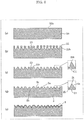
- FIG. 7 is a schematic cross-sectional view illustrating the steps of forming wavelength conversion member 4 in the process of manufacturing wavelength conversion element 1 according to the present embodiment.
- fluorescent substance-containing material 24 is disposed such that openings 25a are sufficiently filled with fluorescent substance-containing material 24.
- fluorescent substance-containing material 24 is injected into openings 25a to an extent such that fluorescent substance-containing material 24 overflows from openings 25a.
- support member 2 including fluorescent substance-containing material 24 on supporting surface 2m is then heated in a high temperature furnace to cure liquid binder material 24b in fluorescent substance-containing material 24.
- wavelength conversion member 4 is formed.
- openings 25a have a diameter smaller than the width of support member 2.
- Such a configuration can achieve wavelength conversion member 4 having width W3 smaller than width W1 of support member 2 as illustrated in FIG. 1 .
- wavelength conversion member 4 may be wet etched to form projecting portions formed of a fluorescent material on the surface of wavelength conversion member 4 and depressed portions formed of transparent binder 4b.
- Wavelength conversion element 1 including depressions and projections having inclinations 2a in support member 2 can be readily manufactured by the manufacturing process described above. Because a layer of a particulate material having a high refractive index is not included between wavelength conversion member 4 and support member 2 in the present embodiment, heat generated in wavelength conversion member 4 can be efficiently dissipated to support member 2.
- FIG. 8 is a diagram schematically illustrated in a measurement system used in an experiment to verify the advantageous effects of wavelength conversion element 1 according to the present embodiment.
- FIG. 9 shows graphs of the results of the experiment to verify the advantageous effects of wavelength conversion element 1 according to the present embodiment.
- the measurement was performed with the measurement system illustrated in FIG. 8 where the surface state (state of supporting surface 2m) of the support member was varied as the following three states:
- the measurement was performed using support members having these surface states (a), (b), and (c), and the results are shown in graphs (a), (b), and (c) of FIG. 9 , respectively.
- the abscissa represents the emitting direction angle
- the ordinate represents the intensity of reflected light.
- the depressions and projections having inclinations 2a in support member 2 provide a sufficient scattering effect.
- the depressions and projections having inclinations 2a the depressions and projections formed by grinding have a higher scattering effect. It is believed that this higher scattering effect is attributed to the differences between the shape and dimension of depressions and projections having inclinations 2a in support member 2 and those of the depressions and projections formed by grinding.
- depressed portions 2c of the depressions and projections having inclinations 2a in support member 2 have a depth of 1 ⁇ m or more and 4 ⁇ m or less in terms of a peak-to-valley value a 50 ⁇ m square region.
- the ratio of the depth to the width of depressed portions 2c is 0.1 or more and 1 or less.
- depressions and projections which can sufficiently scatter incident light 82 can be readily formed around wavelength conversion member 4 on supporting surface 2m of support member 2 of wavelength conversion element 1.
- a reduction in conversion efficiency of the wavelength conversion member caused by an increased temperature of wavelength conversion member 4 can be prevented, and efficient scattering of incident light not radiated to wavelength conversion member 4 can be achieved, efficiently emitting emitted light from wavelength conversion member 4.
- wavelength conversion element 1 According to the present embodiment,
- FIG. 10 is a schematic cross-sectional view illustrating other effects of wavelength conversion element 1 according to the present embodiment.
- Cross-sectional view (b) of FIG. 10 illustrates a relative positional deviation between incident light 82 and wavelength conversion member 4.
- incident light 82 is radiated to the surface (supporting surface 2m) of support member 2 in wavelength conversion element 1
- incident light 82 keeping directivity is not reflected on support member 2, as described above, because support member 2 has the depressions and projections which performs diffusion reflection on incident light 82.
- a light emitting device including wavelength conversion element 1 does not emit reflected light 97 keeping directivity illustrated in FIG. 8 , ensuring safety also in lighting apparatuses and devices which illuminate people.
- wavelength conversion member 4 may be formed by mixing or laminating a blue fluorescent substance which emits blue fluorescence and a yellow fluorescent substance which emits yellow fluorescence.
- the reflective film is not formed in outer peripheral region 2e of supporting surface 2m, and is formed only in arrangement region 2p immediately under wavelength conversion member 4.
- silicon is exposed.
- Silicon has a reflectance of 40% to incident light 82 (excitation light 81) having a wavelength of 450 nm.
- incident light 82 excitation light 81
- part of incident light 82 i.e., peripheral light components 82b directly enter surface (i.e., supporting surface 2m) of support member 2.
- peripheral light components 82b are scattered by depressions and projections having inclinations 2a in light scattering portion 2s, and part of peripheral light components 82b is absorbed by support member 2 formed of silicon.
- the absorption coefficient of excitation light in light scattering portion 2s is larger than the absorption coefficient of excitation light in arrangement region 2p, and the absorption coefficient of excitation light in light scattering portion 2s may be at least equal to the absorption coefficient of excitation light in arrangement region 2p.
- a wavelength conversion element according to Modification 2 of the present embodiment will now be described with reference to the drawing.
- wavelength conversion element 1b As illustrated in FIG. 12 , in wavelength conversion element 1b according to the present modification, depressions and projections having inclinations 2a are formed only in light scattering portion 2s in outer peripheral region 2e of supporting surface 2m but not in arrangement region 2p. In other words, in the present modification, light scattering portion 2s has a surface roughness at least equal to that of arrangement region 2p. Also in this case, incident light which enters wavelength conversion member 4 is scattered by fluorescent material 4a, and the emission of incident light which is not scattered is prevented.
- a wavelength conversion element according to Modification 3 of the present embodiment and a light emitting device including the wavelength conversion element will now be described with reference to the drawings.
- FIG. 14 is a schematic cross-sectional view illustrating a positional relation between wavelength conversion element 1c according to the present modification and incident light 82.
- FIG. 15 is a schematic perspective view illustrating light projector 201 including wavelength conversion element 1c according to the present modification and projected light 299 therefrom.
- Wavelength conversion element 1c according to the present modification and light projector 201 including wavelength conversion element 1c are used in headlamps for vehicles.
- wavelength conversion member 4c disposed on support member 2 is patterned into a hook shape as illustrated in FIG. 13 .
- pattern 204d corresponding to cutoff points of headlamps for vehicles is formed on wavelength conversion member 4c.
- the irradiation region of incident light 82 in wavelength conversion element 1c includes part of wavelength conversion member 4c such that pattern 204d of wavelength conversion member 4c is located near the center of the irradiation region.
- FIG. 13 illustrates the irradiation region of incident light 82 in wavelength conversion element 1c
- light emitting device 60c including wavelength conversion element 1c according to the present modification and projected light 299 emitted from light projector 201 including projecting member 33, such as a projection lens, will be described with reference to FIG. 15 .
- projected light 299 emitted from light projector 201 is white light having a clear cutoff pattern.
- wavelength conversion element 1c can achieve light emitting device 60c and light projector 201 having high luminance and enabling easy patterning of projected light.
- the wavelength conversion element according to the present embodiment includes a light scattering portion having a configuration different from that of wavelength conversion element 1 according to Embodiment 1. Differences between the wavelength conversion element according to the present embodiment and wavelength conversion element 1 according to Embodiment 1 will be mainly described with reference to FIG. 16 .
- FIG. 16 is a schematic cross-sectional view illustrating a configuration of wavelength conversion element 301 according to the present embodiment.
- wavelength conversion element 301 mainly includes support member 2, wavelength conversion member 304, and scattering member 102.
- wavelength conversion member 304 formed of a fluorescent ceramic plate is disposed on supporting surface 2m of support member 2.
- Wavelength conversion member 304 is formed of a fluorescent plate formed by mixing Al 2 O 3 and Ce-doped (Ga, Y, Gd) 3 Al 5 O 10 and sintering the mixture, for example.
- the central portion of supporting surface 2m of support member 2 includes undercoating 111 formed of a laminate film of a metal such as Ti, Pt, or Au.
- Scattering member 102 is disposed in outer peripheral region 2e of supporting surface 2m so as to surround wavelength conversion member 304.
- Scattering member 102 is formed by dispersing particles 102b of TiO 2 , ZrO 2 , Al 2 O 3 , BN, or AlN having a high refractive index in transparent binder 102c formed of a material, such as silicone or a glass material, having a refractive index lower than that of particles 102b having a high refractive index, for example. Fine depressions and projections 102a are formed on the surface of scattering member 102.
- the light scattering portion is scattering member 102 disposed on supporting surface 2m and containing particles 102b having a high refractive index and transparent binder 102c.
- scattering member 102 is one example of the first scattering member described above.
- the total length of scattering member 102 and arrangement region 2p in a direction parallel to supporting surface 2m is preferably 2.2 ⁇ 2 ⁇ 0 or more where the diameter of incident light 82 is 2 ⁇ 0 .
- central light components 82a of incident light 82 are radiated to wavelength conversion member 304.
- Part of central light components 82a propagates through wavelength conversion member 304, undergoes multiple reflection by reflective film 112 disposed immediately under wavelength conversion member 304 and interface 102d between wavelength conversion member 304 and scattering member 102, and is converted into multiple reflection light 85a.
- white light 91 formed of scattered light 92a and fluorescence 93 can be efficiently generated, and be emitted from wavelength conversion member 304.
- peripheral light components 82b of incident light 82 are radiated to scattering member 102.
- Peripheral light components 82b are scattered or totally reflected by fine depressions and projections 102a on the surface of scattering member 102 and particles 102b having a high refractive index of scattering member 102, and are emitted from wavelength conversion element 301 as scattered light 92b.
- part of incident light 82 which enters from the outside of wavelength conversion element 301 and is radiated to portions other than wavelength conversion member 304 can be also scattered by the surface of scattering member 102 disposed around wavelength conversion member 304.
- wavelength conversion element 301 Even in the case where incident light 82 or excitation light having high directivity enters wavelength conversion element 301, the reflection of incident light 82 on support member 2 while keeping directivity can be prevented. As a result, the emission of unnecessary stray light having high directivity from wavelength conversion element 301 can be prevented. Furthermore, even when some components of incident light which enter wavelength conversion member 304 reach the lateral surfaces of wavelength conversion member 304, these components are again reflected in wavelength conversion member 304 by interface 102d with scattering member 102 disposed on the lateral surfaces of wavelength conversion member 304. For this reason, incident light 82 can be efficiently converted into fluorescence within wavelength conversion member 304. As a result, emitted light having high luminance can be emitted from wavelength conversion member 304.
- the surface of scattering member 102 that is, the interface between scattering member 102 and its surrounding air has depressions and projections in the present modification
- the surface of scattering member 102 may have no depressions and projections.
- depressions and projections are formed at the interface between particles 102b having a high refractive index and transparent binder 102c along the shapes of particles 102b having a high refractive index.
- scattering member 102 has depressions and projections at the interface between particles 102b having a high refractive index and transparent binder 102c, and incident light which enter the inside of scattering member 102 is scattered by the depressions and projections.
- wavelength conversion element according to Modification 1 of the present embodiment will now be described. Unlike wavelength conversion element 301 according to Embodiment 2, the wavelength conversion element according to the present modification also includes scattering member 102 in arrangement region 2p of supporting surface 2m. Differences between the wavelength conversion element according to the present modification and wavelength conversion element 301 according to Embodiment 2 will be mainly described with reference to the drawing.
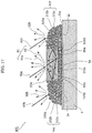
- FIG. 17 is a schematic cross-sectional view illustrating a configuration of wavelength conversion element 401 according to the present modification.
- scattering member 102 is also disposed in arrangement region 2p.
- scattering member 102 covers all of surfaces of wavelength conversion member 304 disposed in arrangement region 2p excluding the surface which incident light 82 enters (upper surface of FIG. 17 ), i.e., the lateral surfaces and the surface facing support member 2.
- scattering member 102 also functions as a reflective member which is disposed between wavelength conversion member 304 and support member 2 and is different from support member 2.
- scattering member 102 is one example of the second scattering member described above.
- part of incident light 82 which enters wavelength conversion member 304 can be subjected to multiple reflection by interface 102d between wavelength conversion member 304 and scattering member 102 disposed in outer peripheral region 2e and interface 102e between wavelength conversion member 304 and scattering member 102 disposed between wavelength conversion member 304 and support member 2.
- white light 91 can be efficiently emitted from wavelength conversion member 304.
- Comparative Example 1 and Embodiment 2 show that at a power of incident light of 2 W or more, scattering member 102 disposed around wavelength conversion member 304 can improve the peak luminance. Furthermore, the graph shows that irrespective of the power of incident light, the peak luminance can be significantly improved by scattering member 102 disposed on both of the lateral surfaces and the bottom surface of wavelength conversion member 304 as in wavelength conversion element 401 according to Modification 1 of Embodiment 2 illustrated in FIG. 17 .
- FIG. 18B is a luminance distribution chart showing the results of measurement of the luminance of the emitted light of the wavelength conversion element according to the emission position in wavelength conversion element 401 according to Modification 1 of the present embodiment where the power of incident light is 3 W.
- FIG. 18C is a luminance distribution chart showing the results of measurement of the luminance of the emitted light of the wavelength conversion element according to the emission position in the wavelength conversion element of Comparative Example 2.
- width W3 of the wavelength conversion member is sufficiently larger than that of the wavelength conversion element according to Modification 1 of the present embodiment. In other words, the wavelength conversion member has a width sufficiently larger than the diameter of the incident light.
- a broad high luminance region is formed near the center of the emission region of the wavelength conversion element, and the luminance sharply decreases from the high luminance region toward the surrounding low luminance region.
- a luminance distribution better than that of Comparative Example 2 can be achieved through adjustment of the width of the wavelength conversion member and the width of the incident light.
- light projectors having a high illuminance region corresponding to the shape of the wavelength conversion member and having a low illuminance in the surrounding region can be achieved.
- light projectors having excellent illuminance distribution properties can be achieved.
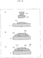
- FIG. 19 is a schematic cross-sectional view illustrating of the steps in the process of manufacturing wavelength conversion element 401 according to the present modification.
- the workpiece is heated at about 150°C for two hours to volatilize the organic solvent in paste 124 for a scattering member and cure paste 124 for a scattering member.
- scattering member 102 can be formed on the bottom surface and lateral surfaces of wavelength conversion member 304.
- paste 124 for a scattering member contracts, depressions and projections can be readily formed along particles 102b having a high refractive index on the surface of scattering member 102.
- FIG. 20 shows graphs of the results of measurement of the angle dependency of intensity of reflected light in scattering member 102 using the measurement system illustrated in FIG. 8 where scattering member 102 is disposed on a silicon substrate or support member 2.
- Graph (a) of FIG. 20 shows results of measurement in the case where only support member 2 is disposed (that is, scattering member 102 is not disposed).
- Graph (b) of FIG. 20 shows results of measurement in the case where scattering member 102 is disposed on support member 2, scattering member 102 containing TiO 2 particles having a particle diameter distribution of 0.1 ⁇ m to 0.7 ⁇ m as particles 102b having a high refractive index.
- scattering member 102 shows the results of measurement in the case where scattering member 102 is disposed on support member 2, scattering member 102 containing TiO 2 particles having a particle diameter distribution of 0.2 ⁇ m to 5 ⁇ m as particles 102b having a high refractive index.
- particle diameter distribution of 0.1 ⁇ m to 0.7 ⁇ m indicates that the average particle size (median diameter) D50 is 0.3 ⁇ m, the average particle size D10 is 0.1 ⁇ m, and the average particle size D90 is 0.7 ⁇ m.
- particle diameter distribution of 0.2 ⁇ m to 5 ⁇ m indicates that the average particle size (median diameter) D50 is 1.9 ⁇ m, the average particle size D10 is 0.2 ⁇ m, and the average particle size D90 is 5 ⁇ m.
- FIG. 21 is a graph showing the relation between the particle diameter of particles 102b having a high refractive index and the degree of scattering.
- the index of the degree of scattering was defined as the ratio (ratio of intensity) of the intensity of light at a radiation angle of 70° to the intensity of light at a radiation angle of 0°.
- ratio of intensity the ratio of intensity of the intensity of light at a radiation angle of 70° to the intensity of light at a radiation angle of 0°.
- a strong peak is generated in the case where incident light entering from a direction of -70° is reflected while keeping directivity.
- the ratio of intensity linearly reduces as particles 102b having a high refractive index have a larger average particle size.
- a preferred average particle size D50 of particles 102b having a high refractive index forming scattering member 102 is 1 ⁇ m to 10 ⁇ m where the ratio of intensity is 2 or less.
- wavelength conversion element according to Modification 2 of the present embodiment will now be described.
- the wavelength conversion element according to the present modification includes another scattering member, which is different from scattering member 102 surrounding wavelength conversion member 304, between wavelength conversion member 304 and support member 2.
- Differences between the wavelength conversion element according to the present modification and wavelength conversion element 401 according to Modification 1 of Embodiment 2 will be mainly described below with reference to the drawings.
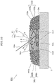
- wavelength conversion element 501 includes scattering member 202 disposed between wavelength conversion member 304 and support member 2, scattering member 202 being different from scattering member 102 surrounding wavelength conversion member 304.
- Scattering member 202 is one example of the second scattering member described above.
- Scattering member 202 to be used may be a scattering member containing dispersed particles having a high refractive index, which are different in material and average particle size from those of scattering member 102 which surrounds wavelength conversion member 304. Such a configuration can improve the freedom in configuration of scattering member which covers the bottom surface and lateral surfaces of wavelength conversion member 304.
- Supporting surface 2m of support member 2 may include a reflective film formed of a multi-layer dielectric film or a metal reflective film.
- a metal film to be used can be a film formed of Ag, for example.
- Such a configuration having a double reflection structure of scattering member 202 and reflective film 3 can efficiently reflect multiple reflection light 85a traveling from wavelength conversion member 304 to support member 2 even if scattering member 202 disposed between wavelength conversion member 304 and support member 2 has a small thickness.
- the scattering member can also have a small thickness even when a transparent binder having a low thermal conductivity is used as a material for the scattering member disposed between wavelength conversion member 304 and support member 2. For this reason, heat generated in wavelength conversion member 304 can be efficiently dissipated to support member 2.
- the scattering member disposed between wavelength conversion member 304 and support member 2 preferably has a thickness of 1 ⁇ m or more and 50 ⁇ m or less.
- the configuration including the reflective film described above may be used in the configuration of Embodiment 2 illustrated in FIG. 17 .
- antireflective film 160 formed of a multi-layer dielectric film may be disposed between wavelength conversion member 304 and the surface of scattering member 102.
- wavelength conversion member 304 and scattering member 102 having fine depressions and projections 102a on the surface are formed on support member 2, and then a dielectric multi-layer dielectric film can be formed by a film forming method such as sputtering. Because the configuration of the present modification can prevent the reflection of incident light 82 on the surface of wavelength conversion member 304, incident light 82 can efficiently enter wavelength conversion member 304.
- the configuration including the antireflective film may also be used in the configuration of Embodiment 2 illustrated in FIG. 17 .
- wavelength conversion element according to Modification 3 of the present embodiment will now be described.
- the wavelength conversion element according to the present modification includes a configuration which can provide compatibility between the reflection properties and heat dissipating properties between wavelength conversion member 304 and support member 2. Differences between the wavelength conversion element according to the present modification and wavelength conversion element 401 according to Modification 1 of Embodiment 2 will be mainly described below with reference to the drawings.
- undercoating 111 formed of a metal film of Ti, Pt, or Au is formed on supporting surface 2m of support member 2, and reflective film 112 formed of Pt, Ag, Ti, Pt, or Au is formed on part of the surface of wavelength conversion member 304 facing support member 2.
- Bonding layer 113 such as Au bumps is disposed on undercoating 111 to bond reflective film 112 to undercoating 111.
- Support member 2 including undercoating 111 and bonding layer 113 will now be described with reference to the drawing.
- FIG. 24 is a schematic plan view illustrating a configuration of support member 2, undercoating 111, and bonding layer 113 according to the present modification.
- FIG. 24 is a plan view of support member 2 in a top surface view of supporting surface 2m.
- undercoating 111 is disposed in the center of supporting surface 2m of support member 2. Furthermore, bonding layer 113 is disposed on undercoating 111. In the example illustrated in FIG. 24 , a plurality of bonding layers 113 is disposed on undercoating 111. The position where bonding layers 113 are disposed corresponds to the position of reflective film 112 disposed in wavelength conversion member 304.
- Wavelength conversion member 304 is then disposed such that each of bonding layers 113 contacts reflective film 112 as illustrated in FIG. 24 . Thereby, reflective film 112 is bonded to undercoating 111.
- Scattering member 102 is disposed in a portion between wavelength conversion member 304 and support member 2 where bonding layers 113 are not disposed.
- scattering member 102 is one example of the second scattering member described above.
- a usable process of manufacturing scattering member 102 is a process of disposing paste 124 for a scattering member between wavelength conversion member 304 and support member 2 using a capillary phenomenon, and heating the workpiece. Such a configuration enables design of the configuration for reflection on the bottom surface of wavelength conversion member 304 with higher freedom, and heat generated in wavelength conversion member 304 can be readily dissipated to support member 2 through bonding layers 113.
- FIG. 25 is a diagram showing the materials examined as material for the support member of the wavelength conversion element according to the present disclosure and their properties.
- the properties of the materials shown in FIG. 25 are the coefficient of thermal expansion, the thermal conductivity, and the reflectance.
- the material to be used in the support member preferably has a coefficient of thermal expansion as close to the coefficient of thermal expansion of glass as possible and a high thermal conductivity as possible.
- silicon is used for the support member in the wavelength conversion elements according to the embodiments and the modifications from the viewpoints described above and the viewpoint of cost, other materials may also be used.
- SiC silicon carbide
- use of silicon carbide (SiC) for the support member can prevent an increase in temperature of the wavelength conversion member, and therefore the conversion efficiency of an excited fluorescent substance can be kept.
- use of silicon carbide (SiC) enables efficient diffuse reflection of excitation light or fluorescence by the support member, and thus an improvement in luminance of the light emitting device.
- support member 2 may be formed of a material having low reflectance to the light corresponding to the wavelength of excitation light, that is, having high absorptivity.
- the wavelength conversion element according to the present embodiment include a substrate formed of diamond as a support member.
- the configuration of the support member of the wavelength conversion element according to the present embodiment and the manufacturing process will now be described with reference to the drawings.
- seed substrate 720 for forming support member 702 formed of diamond is prepared.
- diamond is grown on the main surface of seed substrate 720 to form support member 702.
- diamond can be formed by a high pressure synthetic process or a gaseous phase synthetic process, for example.
- the gaseous phase synthetic process to be used can be microwave plasma CVD.
- microwave plasma CVD diamond crystals can be grown under an atmosphere of reduced pressure using plasma formed by microwave discharging in a stream of hydrogen and methane gas.
- diamond crystal growth conditions are controlled to form a second crystal face on the surface, the second crystal face being different from a first crystal face forming a main surface.
- inclinations 702a are formed on support member 702.
- reflective film 3 is formed on the surface of support member 702.
- wavelength conversion member 4 is formed on support member 702 through a step similar to the step illustrated in FIG. 7 . Thereby, wavelength conversion element 701 can be formed.
- Wavelength conversion element 701 according to the present embodiment can also achieve the effects similar to those of wavelength conversion element 1 according to Embodiment 1. Furthermore, because support member 702 of wavelength conversion element 701 has high thermal conductivity, an increase in temperature of wavelength conversion member 4 can be prevented even when excitation light having high intensity is radiated. For this reason, a reduction in conversion efficiency of fluorescent material 4a within wavelength conversion member 4 can be prevented. Accordingly, a light emitting device including wavelength conversion element 701 according to the present embodiment can have an improved luminance.
- a light emitting device according to Embodiment 4 will now be described. Unlike light emitting device 60 described in Embodiment 1, the light emitting device according to the present embodiment includes an optical fiber as a propagation path of excitation light. The light emitting device according to the present embodiment will now be described with reference to the drawings.
- FIG. 27 is a schematic cross-sectional view illustrating a configuration of light emitting device 801 according to the present embodiment.
- light emitting device 801 includes excitation light source 40, lens 31, optical fiber 36 and light emitter 860.
- Light emitter 860 includes wavelength conversion element 1, fixing member 50, and lens 32.
- excitation light 81 emitted from excitation light source 40 is converged through lens 31.
- the converged excitation light 81 is then connected to optical fiber 36, and propagates through optical fiber 36.
- Propagating light 883 emitted from optical fiber 36 is converted into incident light 82 as converged light through lens 32 of light emitter 860.
- Incident light 82 is radiated to wavelength conversion member 4 in wavelength conversion element 1.
- Incident light 82 is then converted into scattered light 92a and fluorescence 93 by wavelength conversion member 4 and support member 2.
- Scattered light 92a and fluorescence 93 are emitted from transparent cover member 35 as white emitted light 95 to be emitted from wavelength conversion element 1.
- Scattered light 92a is light subjected to diffuse reflection by fluorescent material 4a and support member 2.
- Fluorescence 93 is light having a wavelength converted by fluorescent material 4a and scattered by fluorescent material 4a and support member 2.
- the wavelength conversion elements and light emitting devices according to the present disclosure can have a high luminance and an illuminance distribution which can be readily controlled, and are useful in a variety of lighting apparatuses and devices, such as headlamps for vehicles and light sources for spotlights.
Landscapes
- Engineering & Computer Science (AREA)
- General Engineering & Computer Science (AREA)
- Physics & Mathematics (AREA)
- Optics & Photonics (AREA)
- Semiconductor Lasers (AREA)
- Led Device Packages (AREA)
- Optical Filters (AREA)
- Optical Elements Other Than Lenses (AREA)
Abstract
Description
- The present disclosure relates to wavelength conversion elements which can be used in a variety of lighting apparatuses and devices, such as headlamps for vehicles and light sources for spotlights, and light emitting devices including the wavelength conversion elements.
- Wavelength conversion elements which can be used in a variety of lighting apparatuses and devices, such as headlamps for vehicles and light sources for spotlights, and light emitting devices including the wavelength conversion elements are known in the related art (for example, see PTL 1). A light emitting device disclosed in
PTL 1 will now be described with reference to the drawings.FIG. 28A is a side view illustratinglight emitting device 900 disclosed inPTL 1.FIG. 28B is an enlarged view ofwavelength conversion element 914 andmount substrate 10 disclosed inPTL 1. - As illustrated in
FIG. 28A ,light emitting device 900 includesmount substrate 910 includingwiring layer 916a,light emitting element 912 disposed on wiring layer 916 ofmount substrate 910, andwavelength conversion element 914 disposed onmount substrate 910. As illustrated inFIG. 28B ,wavelength conversion element 914 includessubstrate 920,layer 922 of a particulate material having a high refractive index,fluorescent layer 924, and inorganictransparent material layer 926 disposed in sequence onsubstrate 920. - In
light emitting device 900,fluorescent layer 924 is irradiated with laser light emitted fromlight emitting element 912.Fluorescent layer 924 absorbs part of the laser light emitted fromlight emitting element 912 as excitation light, and emits fluorescence. Part of the laser light emitted fromlight emitting element 912 and not absorbed byfluorescent layer 924 and the fluorescence emitted fromfluorescent layer 924 are scattered by at least one offluorescent layer 924 andlayer 922 of a particulate material having a high refractive index, and are emitted fromlight emitting device 900. - PTL 1: Japanese Unexamined Patent Application Publication No.
2010-10560 - In
light emitting device 900 disclosed inPTL 1, the region to be irradiated with emitted light has a shape corresponding to the shape offluorescent layer 924 in a top surface view ofsubstrate 920. To control the shape of the region to be irradiated with emitted light such that the shape of the region corresponds to the shape offluorescent layer 924,fluorescent layer 924 should be irradiated with laser light such that the end offluorescent layer 924 is covered with the laser light. In this case, part of the laser light emitted fromlight emitting element 912 is radiated to portions outsidefluorescent layer 924, and is emitted fromlight emitting device 900 as non-scattered stray light. The stray light may affect the illuminance distribution properties oflight emitting device 900. - An object of the present disclosure is to provide a wavelength conversion element which can prevent the emission of incident light (that is, excitation light) which is not scattered, and a light emitting device including the wavelength conversion element.
- To solve the problem, one aspect of the light emitting device according to the present disclosure is a light emitting device including a wavelength conversion element, and an excitation light source which emits excitation light to the wavelength conversion element. The wavelength conversion element includes a support member having a supporting surface, and a wavelength conversion member disposed on the supporting surface of the support member so as to be contained within the support member in a top surface view of the support member. An outer peripheral region of the support member exposed from the wavelength conversion member corresponds to an outer peripheral portion of an arrangement region where the wavelength conversion member is disposed. The outer peripheral region of the support member includes a light absorbing portion which can absorb first light having a wavelength identical to the wavelength of the excitation light or a light scattering portion which can scatter the first light.
- In such a configuration, at least part of incident light (that is, excitation light) which does not enter the wavelength conversion member is absorbed or scattered by the outer peripheral region, preventing the emission of the incident light which is not scattered after entering the wavelength conversion element from the excitation light source. Accordingly, a light emitting device having excellent illuminance distribution properties can be achieved.
- Furthermore, in one aspect of the light emitting device according to the present disclosure, the first light may be the excitation light.
- In such a configuration, the excitation light entering the outer peripheral region on the support member can be absorbed, preventing the excitation light entering the outer peripheral region from being emitted from light emitting device. For this reason, a light emitting device having excellent illuminance distribution properties can be achieved.
- Furthermore, in one aspect of the light emitting device according to the present disclosure, in the arrangement region, a reflective member may be disposed between the wavelength conversion member and the support member.
- In such a configuration, the excitation light entering the wavelength conversion member and the fluorescence having a wavelength converted by the wavelength conversion member can be reflected by the reflective member, and be emitted as emitted light. Accordingly, the light emitting device can emit light having improved luminance.
- Furthermore, in one aspect of the light emitting device according to the present disclosure, the support member may contain silicon, silicon carbide, sapphire, or diamond as a material used in the support member, and the excitation light may directly enter a surface of the support member.
- Such a configuration can enhance the thermal conductivity of the support member, improving the heat dissipating properties of the support member.
- Furthermore, in one aspect of the light emitting device according to the present disclosure, the light scattering portion may have a surface including depressions and projections.
- In such a configuration, the incident light can be scattered by the depressions and projections, preventing the emission of the excitation light which is not scattered after entering the wavelength conversion element from excitation light source.
- Furthermore, in one aspect of the light emitting device according to the present disclosure, the depressions and projections may have inclinations formed on the support member.
- Such a configuration can scatter the incident light on the depressions and projections having the inclinations, preventing the emission of the excitation light which is not scattered after entering the wavelength conversion element from the excitation light source.
- Furthermore, in one aspect of the light emitting device according to the present disclosure, the inclinations may also be formed in the arrangement region.
- In such a configuration, the excitation light entering the wavelength conversion member and the fluorescence having a wavelength converted by the wavelength conversion member can be scattered by the inclinations. For this reason, the generation of the excitation light emitted without being scattered can be prevented.
- Furthermore, in one aspect of the light emitting device according to the present disclosure, the depressions and projections may be disposed on a surface of a scattering member, which is disposed on the support member, and contains particles having a high refractive index and a transparent binder.
- Such a configuration enables the formation of the light scattering portion without processing the surface of the support member. The properties of the light scattering portion can be controlled with higher freedom.
- Furthermore, in one aspect of the light emitting device according to the present disclosure, the light scattering portion may be a scattering member, which is disposed on the support member, and contains particles having a high refractive index and a transparent binder.
- Such a configuration enables the formation of the light scattering portion without processing the surface of the support member. The properties of the light scattering portion can be controlled with higher freedom.
- To achieve the object of the present disclosure, the wavelength conversion element according to the present disclosure includes a support member having a supporting surface, and a wavelength conversion member disposed on the supporting surface and containing a fluorescent material which absorbs excitation light and generates fluorescence. The supporting surface includes an arrangement region where the wavelength conversion member is disposed, and an outer peripheral region disposed outside the arrangement region and exposed from the wavelength conversion member. The outer peripheral region includes a light scattering portion having depressions and projections at an interface of the light scattering portion.
- In such a configuration, at least part of the excitation light not entering the wavelength conversion member is scattered by the depressions and projections of the light scattering portion. For this reason, the emission of the excitation light which is not scattered can be prevented in the case where the excitation light enters the wavelength conversion element from the excitation light source. Accordingly, a light emitting device having excellent illuminance distribution properties can be achieved.
- Furthermore, in one aspect of the wavelength conversion element according to the present disclosure, the arrangement region may include a reflective member disposed between the wavelength conversion member and the support member.
- In such a configuration, the excitation light and the fluorescence having a wavelength converted by the wavelength conversion member can be reflected by the reflective member in the case where the excitation light enters the wavelength conversion member. For this reason, light having enhanced luminance can be emitted from the wavelength conversion element.
- Furthermore, in one aspect of the wavelength conversion element according to the present disclosure, the support member may be a crystalline substrate.
- In such a configuration, depressions and projections having a desired structure can be formed through anisotropic etching of the surface of the support member.
- Furthermore, in one aspect of the wavelength conversion element according to the present disclosure, the depressions and projections have inclinations disposed on the supporting surface. The depressions and projections have depressed portions having a depth of 1 µm or more and 4 µm or less. The ratio of the depth to the width of the depressed portions is 0.1 or more and 1 or less.
- Such a configuration can achieve a sufficient scattering effect of the light scattering portion.
- Furthermore, in one aspect of the wavelength conversion element according to the present disclosure, the light scattering portion has a surface roughness at least equal to a surface roughness of the arrangement region.
- Furthermore, in one aspect of the wavelength conversion element according to the present disclosure, the depressions and projections may have vertex portions having a curvature.
- Such a configuration can ensure the scattering of incident light on the vertex portions of the depressions and projections because the vertex portions are not flat.
- Furthermore, in one aspect of the wavelength conversion element according to the present disclosure, the light scattering portion may be a first scattering member disposed on the supporting surface and containing particles having a high refractive index and transparent binder.
- Such a configuration enables the formation of the light scattering portion without processing the surface of the support member. The properties of the light scattering portion can be controlled with higher freedom.
- Furthermore, in one aspect of the wavelength conversion element according to the present disclosure, the reflective member may be a second scattering member.
- Such a configuration enables multiple reflection of part of incident light entering the wavelength conversion member at an interface between the wavelength conversion member and the first scattering member disposed in the outer peripheral region and at an interface between the wavelength conversion member and the second scattering member disposed in the support member, and thus white light can be efficiently emitted from the wavelength conversion member.
- Furthermore, in one aspect of the wavelength conversion element according to the present disclosure, the second scattering member may be formed of a material different from a material for the first scattering member.
- Such a configuration can achieve a higher freedom in the configuration of the scattering member which covers the bottom surface and lateral surfaces of the wavelength conversion member.
- Furthermore, in one aspect of the wavelength conversion element according to the present disclosure, the support member may contain silicon, silicon carbide, sapphire, or diamond as a material to be used.
- Such a configuration can enhance the thermal conductivity of the support member, and can improve the heat dissipating properties of the support member.
- One aspect of the light emitting device according to the present disclosure includes the wavelength conversion element according to any one of the aspects described above, and an excitation light source which emits the excitation light to the wavelength conversion element.
- Such a configuration can prevent the emission of the excitation light which is not scattered after entering the wavelength conversion element from the excitation light source. For this reason, a light emitting device having excellent illuminance distribution properties can be achieved.
- Furthermore, in one aspect of the light emitting device according to the present disclosure, the excitation light may be radiated to the wavelength conversion member and the light scattering portion.
- Such a configuration can prevent the emission of the excitation light which is not scattered, because the excitation light radiated to the light scattering portion is scattered.
- Furthermore, in one aspect of the light emitting device according to the present disclosure, in a cross-section of the supporting surface including an optical axis of the excitation light, a sum of a width of the light scattering portion and a width of the arrangement region in the cross-section may be 2.2 × 2ω0 or more where ω0 represents a distance from a position where the excitation light has a maximum intensity to a position where the excitation light has an intensity of light equal to 1/e2 of the maximum intensity.
- Such a configuration can sufficiently reduce the intensity of the excitation light radiated to portions outside the light scattering portion and wavelength conversion member.
- Furthermore, in one aspect of the light emitting device according to the present disclosure, an absorption coefficient of the excitation light in the light scattering portion may be at least equal to an absorption coefficient of the excitation light in the arrangement region.
- Such a configuration can absorb the excitation light in the light scattering portion, preventing the emission of the excitation light entering the light scattering portion from the light emitting device. For this reason, a light emitting device having excellent illuminance distribution properties can be achieved.
- The present disclosure can provide a wavelength conversion element which can prevent the emission of incident light which is not scattered, and a light emitting device including the wavelength conversion element.
-
-
FIG. 1 is a schematic cross-sectional view illustrating a configuration of the wavelength conversion element according toEmbodiment 1. -
FIG. 2 is a schematic cross-sectional view illustrating the light scattering properties of the wavelength conversion element according toEmbodiment 1. -
FIG. 3 is a diagram illustrating a configuration for fixing the wavelength conversion element according toEmbodiment 1 to a fixing member. -
FIG. 4 is a schematic cross-sectional view illustrating a configuration of a light emitting device and a light projector according toEmbodiment 1. -
FIG. 5 is a graph illustrating the relation between the quantity of light radiated to portions outside the light scattering portion and the sum of the width of the light scattering portion and the width of the arrangement region when the wavelength conversion element according toEmbodiment 1 is irradiated with incident light having a power of 10 W. -
FIG. 6 is a schematic cross-sectional view illustrating a step of forming a support member in a process of manufacturing the wavelength conversion element according toEmbodiment 1. -
FIG. 7 is a schematic cross-sectional view illustrating a step of forming a wavelength conversion member in the process of manufacturing the wavelength conversion element according toEmbodiment 1. -
FIG. 8 is a diagram schematically illustrating a measurement system used in an experiment to verify the advantageous effects of the wavelength conversion element according toEmbodiment 1. -
FIG. 9 shows graphs of the results of the experiment to verify the advantageous effects of the wavelength conversion element according toEmbodiment 1. -
FIG. 10 is a schematic cross-sectional view illustrating other effects of the wavelength conversion element according toEmbodiment 1. -
FIG. 11 is a schematic cross-sectional view illustrating a configuration of the wavelength conversion element according toModification 1 ofEmbodiment 1. -
FIG. 12 is a schematic cross-sectional view illustrating a configuration of a wavelength conversion element according toModification 2 ofEmbodiment 1. -
FIG. 13 is a schematic plan view illustrating a configuration of a wavelength conversion element according toModification 3 ofEmbodiment 1. -
FIG. 14 is a schematic cross-sectional view illustrating a positional relation between the wavelength conversion element according toModification 3 ofEmbodiment 1 and incident light. -
FIG. 15 is a schematic perspective view illustrating a light projector including the wavelength conversion element according toModification 3 ofEmbodiment 1 and the projected light therefrom. -
FIG. 16 is a schematic cross-sectional view illustrating a configuration of a wavelength conversion element according toEmbodiment 2. -
FIG. 17 is a schematic cross-sectional view illustrating a configuration of a wavelength conversion element according toModification 1 ofEmbodiment 2. -
FIG. 18A is a graph illustrating the relation between the measured value of the power of incident light and the measured value of the peak luminance of emitted light in the wavelength conversion element according toEmbodiment 2 and the wavelength conversion element according toModification 1 ofEmbodiment 2. -
FIG. 18B is a luminance distribution chart showing the results of measurement of the luminance corresponding to each emission position of the emitted light from the wavelength conversion element in the case where the wavelength conversion element according toModification 1 ofEmbodiment 2 is used and incident light has a power of 3 W. -
FIG. 18C is a luminance distribution chart showing the results of measurement of the luminance corresponding to each emission position of the emitted light from the wavelength conversion element in the case where a wavelength conversion element of Comparative Example 2 is used. -
FIG. 19 is a schematic cross-sectional view illustrating steps in a process of manufacturing the wavelength conversion element according toModification 1 ofEmbodiment 2. -
FIG. 20 shows graphs of the results of the angle dependency of the intensity of reflected light in the light scattering portion measured with the measurement system illustrated inFIG. 8 while the light scattering portion is disposed on the support member formed of a silicon substrate. -
FIG. 21 is a graph showing the relation between the particle diameter of particles having a high refractive index and the degree of scattering. -
FIG. 22 is a schematic cross-sectional view illustrating a configuration of a wavelength conversion element according toModification 2 ofEmbodiment 2. -
FIG. 23 is a schematic cross-sectional view illustrating a configuration of a wavelength conversion element according toModification 3 ofEmbodiment 2. -
FIG. 24 is a schematic plan view illustrating a configuration of a support member, an undercoating, and a bonding layer according toModification 3 ofEmbodiment 2. -
FIG. 25 is a table showing materials for a support member of the wavelength conversion element according to the present disclosure examined herein and their properties. -
FIG. 26 is a schematic cross-sectional view illustrating steps in a process of manufacturing a wavelength conversion element according toEmbodiment 3. -
FIG. 27 is a schematic cross-sectional view illustrating a configuration of a light emitting device according toEmbodiment 3. -
FIG. 28A is a side view illustrating a conventional light emitting device. -
FIG. 28B is an enlarged view illustrating a conventional wavelength conversion element and a mount substrate. - Embodiments according to the present disclosure will now be described with reference to the drawings. These embodiments described below are illustrative as preferred specific examples of the present disclosure. Accordingly, numeral values, components, arrangements, positions, and connection forms of the components, steps, order of the steps, and the like shown in the embodiments below are only examples, and will not limit the present disclosure. Among the components of the embodiments below, the components not described in an independent claim representing the most superordinate concept of the present disclosure are described as arbitrary components.
- A wavelength conversion element according to
Embodiment 1 will now be described with reference to the drawings. -
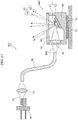
FIG. 1 is a schematic cross-sectional view illustrating a configuration ofwavelength conversion element 1 according to the present embodiment. - As illustrated in
FIG. 1 ,wavelength conversion element 1 according toEmbodiment 1 includessupport member 2 having supportingsurface 2m, andwavelength conversion member 4 disposed on supportingsurface 2m and containingfluorescent material 4a which absorbs excitation light and generates fluorescence. Supportingsurface 2m includesarrangement region 2p includingwavelength conversion member 4, and outerperipheral region 2e disposedoutside arrangement region 2p and exposed fromwavelength conversion member 4. As illustrated,wavelength conversion element 1 includeswavelength conversion member 4 disposed on supportingsurface 2m so as to be contained withinsupport member 2 in a view ofsupport member 2 from supportingsurface 2m side. - Outer
peripheral region 2e of supportingsurface 2m includeslight scattering portion 2s including depressions and projections disposed at the interface. In the present embodiment,light scattering portion 2s includes depressions and projections disposed on the surface ofsupport member 2. More specifically,light scattering portion 2s includes depressions and projections at an interface between supportingsurface 2m and the surrounding air. Furthermore, in the present embodiment, the depressions and projections haveinclinations 2a formed insupport member 2. In the present embodiment,inclinations 2a are also formed inarrangement region 2p. - Such a configuration can scatter incident light 82 on
light scattering portion 2s of supportingsurface 2m even when part of incident light 82 entered from the outside ofwavelength conversion element 1 is radiated to supportingsurface 2m ofsupport member 2 rather than towavelength conversion member 4. For this reason, even when incident light 82 having high directivity enterswavelength conversion element 1, reflection of incident light 82 onsupport member 2 while keeping high directivity can be prevented. As a result, the emission of unnecessary light having high directivity fromwavelength conversion element 1 can be prevented. -
Wavelength conversion element 1 according to the present embodiment including non-essential, optional components will now be more specifically described with reference to the drawings. -
FIG. 2 is a schematic cross-sectional view illustrating the light scattering properties ofwavelength conversion element 1 according to the present embodiment. - As illustrated in
FIG. 1 , inwavelength conversion element 1, depressions and projections havingfine inclinations 2a are disposed in a portion within supportingsurface 2m ofsupport member 2 excludingperipheral portion 2d having width W4. In other words, the internal region of supportingsurface 2m has a structure having depressions and projections. Furthermore, supportingsurface 2m includesreflective film 3. In the present embodiment,wavelength conversion member 4 is disposed in the central portion within a region ofsupport member 2 includinginclinations 2a. In any cross-section ofwavelength conversion element 1intersecting supporting surface 2m, width W2 of theregion including inclinations 2a is smaller than width W1 ofsupport member 2, and width W3 ofwavelength conversion member 4 is smaller than width W2. Part of theregion including inclinations 2a and excludingwavelength conversion member 4 having width W3 corresponds to light scatteringportion 2s. In the present embodiment,light scattering portion 2s having width W5 is disposed so as to surround the outer periphery ofwavelength conversion member 4. - At this time, in the depressions and
projections having inclinations 2a,depressed portions 2c have a depth of 1 µm or more and 4 µm or less in terms of a peak-to-valley value in a 50 µm square region. In other words, the distance between a vertex portion and a bottom in the depressions and projections (distance in the direction vertical to supportingsurface 2m of support member 2) is 1 µm or more and 4 µm or less in a 50 µm square region in supportingsurface 2m. The ratio of the depth to the width is 0.1 or more and 1 or less where the width ofdepressed portion 2c is defined as a distance between adjacent vertices. In the present embodiment, the depressions andprojections having inclinations 2a have shapes varied at random. Such depressions and projections scatter incident light at random, improving the scattering effect of the depressions and projections. -
Wavelength conversion member 4 is, for example, a member formed offluorescent material 4a, or a plurality of fluorescent particles, bonded withtransparent binder 4b. More specifically,fluorescent material 4a to be used is fluorescent particles of a rare earth element-doped fluorescent substance. For example, a yttrium aluminum garnet (YAG), which is a fluorescent substance (Ga, Y, Gd)3-Al5O10 doped with cerium (Ce), is used.Transparent binder 4b to be used is, silicone, silicon oxide, such as a glass material, or a transparent material, such as aluminum oxide or zinc oxide, for example. -
Support member 2 to be used is a substrate formed of a material having high thermal conductivity, specifically, a crystalline substrate, a metal substrate, or a ceramic substrate. In the case wheresupport member 2 is a crystalline substrate, specifically,support member 2 may contain silicon (Si), silicon carbide (SiC), aluminum nitride (AlN), sapphire (Al2O3), or diamond as a material to be used. In the present embodiment,support member 2 to be used is a crystalline silicon substrate formed of silicon.Inclinations 2a are formed onsupport member 2 by performing a process, such as grinding, wet etching, or dry etching, on the surface of a crystalline substrate, a metal substrate, or a ceramic substrate. More preferably, a crystalline substrate is used assupport member 2, andfine inclinations 2a are formed utilizing the crystal orientation ofsupport member 2. Use of such a crystalline substrate leads to precise control of the shape and size ofinclinations 2a. -
Reflective film 3 is a reflective member including a metal film of aluminum (Al), silver (Ag), silver alloy, or platinum (Pt), and a protective film of SiO2 disposed on the metal film, for example. - As illustrated in
FIG. 1 ,wavelength conversion element 1 having such a configuration is irradiated with incident light 82 from immediately above or from a direction approximately oblique towavelength conversion member 4. At this time,wavelength conversion element 1 is irradiated with incident light 82 or laser light having a center wavelength of 420 nm to 490 nm from a distant position, for example. In the laser light which propagates from a distant position, usually, the intensity of light on the optical axis is large, and the intensity of light reduces as the distance from the optical axis increases. In other words, the laser light which propagates from a distant position shows a Gaussian distribution of the intensity as illustrated inlight intensity distribution 83 inFIG. 1 . At this time, among light components of incident light 82, the light components near the optical axis having large intensity of light and radiated towavelength conversion member 4 are referred to ascentral light components 82a, and the light components away from the optical axis having lower intensity of light than that of the light components on the optical axis and not radiated towavelength conversion member 4 are referred to as peripherallight components 82b. - Here, assume that a two-dimensional intensity distribution in a cross-section vertical to the optical axis direction of
incident light 82 is concentrically circular, and the light intensity distribution is an ideal Gaussian distribution. In a cross-section of supportingsurface 2m containing the optical axis of incident light 82, the distance from a position whereincident light 82 has a maximum intensity to a position whereincident light 82 has 1/e2 (about 13.5%) of the maximum intensity is defined as ω0. The diameter of incident light 82 on supportingsurface 2m is defined as 2ω0. In other words, the width of the region where the intensity of light is 1/e2 (about 13.5%) or more of the central intensity (peak intensity) is defined as 2ω0. Furthermore, assume that the shape in a top surface view of wavelength conversion member 4 (in a top surface view of supportingsurface 2m) is circular, and diameter 2ω0 ofincident light 82 is identical to diameter W3 ofwavelength conversion member 4. In this case, about 86.5% of the energy ofincident light 82 is radiated towavelength conversion member 4 while the remaining 13.5% is radiated to the surrounding regions ofwavelength conversion member 4. - In the case where incident light 82 having a power of 10 W enters
wavelength conversion element 1 under such conditions,central light components 82a having a power of about 8.7 W enterwavelength conversion member 4. As illustrated inFIG. 2 , at least part of centrallight components 82a are absorbed byfluorescent material 4a inwavelength conversion member 4, and are converted intofluorescence 93 having a different wavelength.Fluorescence 93 is emitted from the same surface as that ofwavelength conversion member 4, whichincident light 82 enters. Among part offluorescence 93 and light components of incident light 82, those not absorbed byfluorescent material 4a inwavelength conversion member 4 propagate towardsupport member 2. In the present embodiment, a reflective member formed ofreflective film 3 is disposed betweenwavelength conversion member 4 andsupport member 2 inarrangement region 2p. For this reason, the light components which propagate towardsupport member 2 are reflected byreflective film 3. The light components reflected byreflective film 3 are emitted fromwavelength conversion member 4 to the outside ofwavelength conversion element 1 as scattered light 92a orfluorescence 93. As described above,reflective film 3 disposed betweenwavelength conversion member 4 andsupport member 2 can improve the luminance of the light emitted fromwavelength conversion element 1. In the present embodiment, the depressions andprojections having inclinations 2a are also disposed inarrangement region 2p. These depressions and projections can scatter part of light components of incident light 82 which enterwavelength conversion member 4, and reachsupport member 2 without being absorbed byfluorescent material 4a, preventing the emission of incident light which is not scattered after enteringwavelength conversion element 1 fromexcitation light source 40. - As described above,
wavelength conversion member 4 emitswhite light 91 as mixed light offluorescence 93 and scattered light 92a. - In contrast, among the light components of incident light 82 having a light output of 10 W, peripheral
light components 82b having a power of about 1.3 W may be stray light not radiated towavelength conversion member 4. The stray light affects projected images fromwavelength conversion element 1. In the case where light having diameter 2ω0 smaller than diameter W3 ofwavelength conversion member 4 is used as incident light to prevent such stray light, the center ofwavelength conversion member 4 is irradiated with light having significantly large intensity of light. Such light increases the temperature ofwavelength conversion member 4 and reduces the conversion efficiency. Furthermore, in this case, the peripheral portion ofwavelength conversion member 4 is irradiated with only light having small intensity. For this reason, emitted light having a desired distribution shape corresponding to the shape in a top surface view ofwavelength conversion member 4 cannot be achieved. - In the structure of the present embodiment, such peripheral
light components 82b are irregularly reflected (scattered) by depressions andprojections having inclinations 2a disposed onsupport member 2 in the peripheral portion ofwavelength conversion member 4 as illustrated inFIG. 2 . At this time, the directivity ofincident light 82 is lost in the reflected light. For this reason, the conversion of the reflected light into stray light to be emitted in specific directions can be prevented. Furthermore, because peripherallight components 82b are reflected on outerperipheral region 2e ofsupport member 2, the absorption of peripherallight components 82b by the peripheral portion ofwavelength conversion member 4 insupport member 2 can be prevented. Such a configuration can prevent an increase in temperature ofwavelength conversion element 1 caused by heat generated insupport member 2 and a reduction in conversion efficiency ofwavelength conversion member 4. - The process of assembling a light emitting device using
wavelength conversion element 1 according to the present embodiment will now be described with reference to the drawings. - To assemble a light emitting device using
wavelength conversion element 1 according to the present embodiment, a process of fixingwavelength conversion element 1 will first be described. -
FIG. 3 is a diagram illustrating a configuration for fixingwavelength conversion element 1 according to the present embodiment to fixingmember 50. - As illustrated in
FIG. 3 ,wavelength conversion element 1 is fixed to fixingmember 50 usingcontact member 11, holdingmember 12, and screws 13. - Fixing
member 50 is a member for fixingwavelength conversion element 1. Fixingmember 50 includesscrew holes 50a.Wavelength conversion element 1 is disposed on fixingmember 50 withcontact member 11 interposed therebetween. - Holding
members 12 are members for holdingwavelength conversion element 1 down to fixingmember 50. Holdingmembers 12hold support member 2 nearperipheral portion 2d having width W4 on supportingsurface 2m ofsupport member 2 wherewavelength conversion member 4 is not disposed (seeFIG. 1 ). Holdingmembers 12 are fixed to fixingmember 50 by threadedly engagingscrews 13 to screwholes 50a through throughholes 12a of holdingmembers 12. As described above,wavelength conversion element 1 is fixed to fixingmember 50 through fixation of holdingmembers 12, which holdwavelength conversion element 1, to fixingmember 50.Wavelength conversion element 1 fixed using such a configuration is irradiated with incident light 82 as excitation light from above.Incident light 82 is generated by convertingexcitation light 81 emitted fromexcitation light source 40 into substantially parallel light throughlens 31. - Fixing
member 50 is a member formed of a material having high thermal conductivity, such as aluminum, aluminum alloy, surface-plated copper, or copper alloy.Contact member 11 is a sheet-like member formed of a material having high thermal conductivity, such as a graphite sheet, a heat dissipating silicone resin, or a soldering material. - An example in which a light emitting device and a light projector are provided using
wavelength conversion element 1 will now be described with reference to the drawings. -
FIG. 4 is a schematic cross-sectional view illustrating a configuration of light emittingdevice 60 andlight projector 101 according to the present embodiment. - As illustrated in
FIG. 4 , light emittingdevice 60 mainly includeswavelength conversion element 1, fixingmember 50,excitation light source 40, andlens 31.Light projector 101 includes light emittingdevice 60 and projectingmember 33.Light projector 101 may further includeoptical filter 99 having a predetermined transmission spectrum on the emission side of projectingmember 33, for example. - In light emitting
device 60,excitation light source 40 which emitsexcitation light 81 andlens 31 whichexcitation light 81 enters are fixed to fixingmember 50. Although a configuration for fixingwavelength conversion element 1 is not illustrated inFIG. 4 for simplification, light emittingdevice 60 also has a configuration as illustrated inFIG. 3 . In other words,wavelength conversion element 1 is fixed to fixingmember 50 with holdingmembers 12 and screws 13. -
Excitation light source 40 is a semiconductor laser which emits laser light having a wavelength of 420 nm to 490 nm, for example.Excitation light 81 is emitted fromexcitation light source 40 throughlens 31 fixed to fixingmember 50, and is converted intoincident light 82, which is substantially parallel light having high directivity.Incident light 82 then enterswavelength conversion member 4 ofwavelength conversion element 1. - In such a configuration, in
wavelength conversion member 4,incident light 82 is converted into white emitted light 95 including scattered light 92a andfluorescence 93. The white light passes throughtransparent cover member 35 attached to fixingmember 50, and is emitted to the outside of light emittingdevice 60. Inlight projector 101 including light emittingdevice 60, and projectingmember 33, such as a projection lens, disposed on the light path of emitted light 95 (above light emittingdevice 60 inFIG. 4 ), emitted light 95 or white light having high directivity can be emitted by projectingmember 33. Inlight projector 101, fixingmember 50 is fixed toexternal fixing base 75 withheat dissipating mechanism 70 formed of a graphite sheet, for example. Such a configuration can dissipate heat generated inexcitation light source 40 andwavelength conversion element 1 toexternal fixing base 75. - As described above, light emitting
device 60 andlight projector 101 can be provided with a simple configuration usingwavelength conversion element 1 andexcitation light source 40 in the present embodiment.Support member 2 ofwavelength conversion element 1 can be readily fixed to fixingmember 50. Even when the irradiation region with incident light 82 enteringwavelength conversion member 4 is substantially identical to the region wherewavelength conversion member 4 is formed, peripherallight components 82b of incident light 82 reflected on portions other thanwavelength conversion member 4 are scattered by the depressions andprojections having inclinations 2a inlight scattering portion 2s on supportingsurface 2m. For this reason, the emission of peripherallight components 82b from the light emitting device as stray light having high intensity of light in specific directions can be prevented. - A method of designing the dimension of
light scattering portion 2s ofwavelength conversion element 1 will now be described with reference to the drawings. -
FIG. 5 is a graph showing the relation between the quantity of light radiated to the outside oflight scattering portion 2s and sum W2 of the width oflight scattering portion 2s and the width ofarrangement region 2p when incident light 82 having a power of 10 W is radiated towavelength conversion element 1 according to the present embodiment.FIG. 5 shows the relation determined by calculation. The term "quantity of light radiated to the outside oflight scattering portion 2s" indicates the quantity of light components of incident light 82 which are not radiated to both oflight scattering portion 2s andwavelength conversion member 4. - Here, assume that a two-dimensional intensity distribution of incident light 82 on supporting
surface 2m is concentrically circular, and the light intensity distribution is an ideal Gaussian distribution. The abscissa inFIG. 5 represents the ratio of sum W2 of the width oflight scattering portion 2s and the width ofarrangement region 2p to diameter 2ω0 ofincident light 82. The graph shown inFIG. 5 indicates that of incident light 82, the relation represented by W2 ≥ 2.2 × 2 ω0 should be satisfied to control the components to be radiated to the region outsidelight scattering portion 2s having inclinations 2a (that is, the components of incident light 82 which may be converted into stray light) to have a power of 1 mW or less, which is a low-risk level. Herein, the term "light having a power at a low-risk level" indicates light having a power at such a level that the influences of light over the eyes of a person who gazes at the light while blinking can be neglected.Light scattering portion 2s having a dimension thus determined can reduce the influences by stray light and achieve good illuminance distribution properties in the case wherewavelength conversion element 1 is used in the light emitting device. This design method can be used inwavelength conversion member 4 having any shape and in cases whereincident light 82 has a light intensity distribution other than the Gaussian distribution. Where the width of the light intensity distribution ofincident light 82 is defined as width 2ω0 of the region where the intensity of light is 1/e2 or more of peak intensity I0, it is preferred that sum W2 be set in any cross-section ofwavelength conversion element 1 such that the relation represented by W2 ≥ 2.2 × 2 ω0 is satisfied. - Although the irradiation region of the incident light is concentrically circular in the description above, the irradiation region can have any other shape. For example, the irradiation region of the incident light can have an oval shape according to the distribution shape of the incident light or the angle of incidence of the incident light. In this case, it is preferred that the relation of sum W2 of the width of
light scattering portion 2s and the width ofarrangement region 2p and diameter 2ω0 of incident light 82 be established in any cross-section of the irradiation region. - A process of manufacturing
wavelength conversion element 1 will now be described with reference to the drawings. -
FIG. 6 is a schematic cross-sectional view illustrating the steps of formingsupport member 2 in the process of manufacturingwavelength conversion element 1 according to the present embodiment. -
FIG. 7 is a schematic cross-sectional view illustrating the steps of formingwavelength conversion member 4 in the process of manufacturingwavelength conversion element 1 according to the present embodiment. - A step of forming
support member 2 including depressions andprojections having inclinations 2a usingcrystalline substrate 20 will be first described. Here, an example in which a silicon substrate is used ascrystalline substrate 20 will be described. - As illustrated in cross-sectional view (a) of
FIG. 6 , first,crystalline substrate 20 havingfirst crystal face 22a as a main surface is prepared. At this time,first crystal face 22a corresponds to the plane direction <100> of silicon. - In the next step, as illustrated in cross-sectional view (b) of
FIG. 6 , a silicon oxide film oretching mask 21 on the main surface is patterned, and a plurality of second crystal faces 22b is exposed from the main surface ofcrystalline substrate 20 by anisotropy etching. At this time, depressedportions 23 having second crystal faces 22b as lateral surfaces are formed on the main surface ofcrystalline substrate 20. A preferred anisotropy etching process is wet etching using an aqueous solution, such as tetramethylammonium hydroxide (TMAH) or potassium hydroxide (KOH). Second crystal faces 22b of the silicon substrate defined by the plane direction <111> can be exposed by such a wet etching process. At this time, it is preferred that a face having the same crystal face as that of the main surface be not formed on the bottom surfaces ofdepressed portions 23. - Subsequently, as illustrated in cross-sectional view (c) of
FIG. 6 ,etching mask 21 is removed with hydrofluoric acid. Here, as illustrated in partially enlarged view C1 of cross-sectional view (c) ofFIG. 6 ,depressed portion 23 is formed of a combination of planes.Vertex portions 22t formed betweendepressed portions 23 are flat surfaces formed offirst crystal face 22a. Becauseincident light 82, without being scattered, is reflected by such flat surfaces in the case wherevertex portions 22t are irradiated withincident light 82, stray light may be generated. To solve such a problem, as illustrated in cross-sectional view (d) ofFIG. 6 , the edges ofdepressed portions 23 ofcrystalline substrate 20 are removed by etching to formdepressed portions 2c formed of curved faces. Thereby, as illustrated in partially enlarged view D1 of cross-sectional view (d) ofFIG. 6 , depressions andprojections having inclinations 2a formed of curved faces are formed. The depressions and projections includevertex portions 2t having a curvature, anddepressed portions 2c formed of curved faces. Here, use of an isotropic etching process as etching is preferred. Examples of usable isotropic etching processes include a process of performing wet etching using a mixed solution of hydrofluoric acid and nitric acid, and a process of performing dry etching.Depressed portions 2c having a curvature may be formed by the isotropic etching process in this step.Vertex portions 2t may have a curvature of about 1 µm or more and 10 µm or less, for example.Bottoms 2b ofdepressed portions 2c may also have a curvature as invertex portions 2t. - As described above,
support member 2 according to the present embodiment can be formed. - Subsequently, as illustrated in cross-sectional view (e) of
FIG. 6 , for example, silver alloy or aluminum is deposited on the depressions andprojections having inclinations 2a ofsupport member 2 to formreflective film 3. Here,reflective film 3 may include a metal film of silver alloy or aluminum, and an oxidation protective film of SiO2 disposed on the metal film. - A step of forming
wavelength conversion member 4 onsupport member 2 will now be described with reference toFIG. 7 . - As illustrated in cross-sectional view (a) of
FIG. 7 ,mask 25 with openings having predeterminedopenings 25a is first disposed on supportingsurface 2m ofsupport member 2. At this time,wavelength conversion member 4 can be formed into a desired shape by formingopenings 25a according to the desired shape ofwavelength conversion member 4. The thickness ofmask 25 with openings can be set according to the desired thickness ofwavelength conversion member 4. Subsequently, fluorescent substance-containingmaterial 24 containing a mixture offluorescent material 4a andliquid binder material 24b is injected intoopenings 25a ofmask 25 with openings. - Subsequently, as illustrated in cross-sectional view (b) of
FIG. 7 , fluorescent substance-containingmaterial 24 is disposed such thatopenings 25a are sufficiently filled with fluorescent substance-containingmaterial 24. In other words, fluorescent substance-containingmaterial 24 is injected intoopenings 25a to an extent such that fluorescent substance-containingmaterial 24 overflows fromopenings 25a. - As illustrated in cross-sectional view (c) of
FIG. 7 , fluorescent substance-containingmaterial 24overflowing openings 25a is then removed. - As illustrated in cross-sectional view (d) of
FIG. 7 ,support member 2 including fluorescent substance-containingmaterial 24 on supportingsurface 2m is then heated in a high temperature furnace to cureliquid binder material 24b in fluorescent substance-containingmaterial 24. Thereby,wavelength conversion member 4 is formed. In the present embodiment,openings 25a have a diameter smaller than the width ofsupport member 2. Such a configuration can achievewavelength conversion member 4 having width W3 smaller than width W1 ofsupport member 2 as illustrated inFIG. 1 . - In the present embodiment,
liquid binder material 24b to be used can be silsesquioxane dissolved in an organic solvent, for example. - After the curing of
liquid binder material 24b in fluorescent substance-containingmaterial 24,wavelength conversion member 4 may be wet etched to form projecting portions formed of a fluorescent material on the surface ofwavelength conversion member 4 and depressed portions formed oftransparent binder 4b. -
Wavelength conversion element 1 including depressions andprojections having inclinations 2a insupport member 2 can be readily manufactured by the manufacturing process described above. Because a layer of a particulate material having a high refractive index is not included betweenwavelength conversion member 4 andsupport member 2 in the present embodiment, heat generated inwavelength conversion member 4 can be efficiently dissipated to supportmember 2. - The advantageous effects of
wavelength conversion element 1 according to the present embodiment will now be described based on the experimental data. -
FIG. 8 is a diagram schematically illustrated in a measurement system used in an experiment to verify the advantageous effects ofwavelength conversion element 1 according to the present embodiment. -
FIG. 9 shows graphs of the results of the experiment to verify the advantageous effects ofwavelength conversion element 1 according to the present embodiment. - As illustrated in
FIG. 8 , laser light or incident light 96 entered supportingsurface 2m ofsupport member 2 havinginclinations 2a, and the emitting direction angle dependency of reflected light was measured withdetector 94. In the case where the incident surface whichincident light 96 enters is mainly formed of a plane, for example, among the components of incident light 96, components reflected on the incident surface at a reflection angle identical with the angle of incidence (that is, reflected light 97 illustrated inFIG. 8 ) are dominant in the measurement system as illustrated inFIG. 8 . In contrast, in the case where the incident surface has fine depressions and projections,scattered light 98 or scattered reflected light illustrated inFIG. 8 is dominant. - The measurement was performed with the measurement system illustrated in
FIG. 8 where the surface state (state of supportingsurface 2m) of the support member was varied as the following three states: - (a) A surface state of a silicon substrate not processed (surface state where the crystal face is kept),
- (b) A surface state of a silicon substrate having depressions and projections formed by grinding on the surface, and
- (c) A surface state of
support member 2 according to the present embodiment (that is, a surface state having depressions andprojections having inclinations 2a) - The measurement was performed using support members having these surface states (a), (b), and (c), and the results are shown in graphs (a), (b), and (c) of
FIG. 9 , respectively. In each of the graphs ofFIG. 9 , the abscissa represents the emitting direction angle, and the ordinate represents the intensity of reflected light. - As shown in graph (a) of
FIG. 9 , only reflected light 97 having high directivity was observed in the surface state of the silicon substrate not processed. - As shown in graph (b) of
FIG. 9 , it turned out that in the surface state of the silicon substrate having depressions and projections formed by grinding the surface, reflected light 97 keeping directivity (that is, not scattered) is dominant althoughscattered light 98 is observed. In other words, the result shows an insufficient scattering effect by the depressions and projections formed on the surface of the silicon substrate. - As shown in graph (c) of
FIG. 9 , only scattered light 98 was observed, but not reflected light 97, in the surface state ofsupport member 2 according to the present embodiment. - Thus, the depressions and
projections having inclinations 2a insupport member 2 according to the present embodiment provide a sufficient scattering effect. Among the depressions andprojections having inclinations 2a, the depressions and projections formed by grinding have a higher scattering effect. It is believed that this higher scattering effect is attributed to the differences between the shape and dimension of depressions andprojections having inclinations 2a insupport member 2 and those of the depressions and projections formed by grinding. In other words, while the depressed portions of the depressions and projections formed by grinding have a depth in the order of nanometer,depressed portions 2c of the depressions andprojections having inclinations 2a insupport member 2 have a depth of 1 µm or more and 4 µm or less in terms of a peak-to-valley value a 50 µm square region. The ratio of the depth to the width ofdepressed portions 2c is 0.1 or more and 1 or less. - By use of the manufacturing method according to the present embodiment, depressions and projections which can sufficiently scatter incident light 82 can be readily formed around
wavelength conversion member 4 on supportingsurface 2m ofsupport member 2 ofwavelength conversion element 1. As a result, a reduction in conversion efficiency of the wavelength conversion member caused by an increased temperature ofwavelength conversion member 4 can be prevented, and efficient scattering of incident light not radiated towavelength conversion member 4 can be achieved, efficiently emitting emitted light fromwavelength conversion member 4. - Other effects of
wavelength conversion element 1 according to the present embodiment will now be described with reference to the drawings. -
FIG. 10 is a schematic cross-sectional view illustrating other effects ofwavelength conversion element 1 according to the present embodiment. - As illustrated in cross-sectional view (a) of
FIG. 10 , inwavelength conversion element 1 according to the present embodiment, depressions and projections are formed not only onlight scattering portion 2s ofsupport member 2 but also inarrangement region 2p.Wavelength conversion member 4 is disposed onarrangement region 2p where the depressions and projections are formed. Cross-sectional view (a) ofFIG. 10 illustrates a state where incident light 82 or blue laser light enterswavelength conversion element 1, for example. The irradiation region ofincident light 82 is defined such that most ofincident light 82 is radiated towavelength conversion member 4. Unfortunately, a positional deviation between the excitation light source (not illustrated) which generatesincident light 82 andwavelength conversion element 1 may occur during assembly or over time. Cross-sectional view (b) ofFIG. 10 illustrates a relative positional deviation between incident light 82 andwavelength conversion member 4. In this case, althoughincident light 82 is radiated to the surface (supportingsurface 2m) ofsupport member 2 inwavelength conversion element 1, incident light 82 keeping directivity is not reflected onsupport member 2, as described above, becausesupport member 2 has the depressions and projections which performs diffusion reflection onincident light 82. As a result, such a light emitting device includingwavelength conversion element 1 does not emit reflected light 97 keeping directivity illustrated inFIG. 8 , ensuring safety also in lighting apparatuses and devices which illuminate people. - As illustrated in cross-sectional view (c) of
FIG. 10 ,wavelength conversion member 4 may be detached fromsupport member 2 by vibration or impact applied towavelength conversion element 1 during use. In this case, becauseincident light 82 is sufficiently scattered by the surface ofsupport member 2, the safety can also be ensured as in the case of cross-sectional view (b) ofFIG. 10 . - Although blue light having a center wavelength of 420 nm to 490 nm is used as incident light and a YAG fluorescent substance is used as the fluorescent material in the configuration described above, any combination of types of incident light and fluorescent material can be used. For example, in the case where blue light is used as incident light, an Eu-doped α-SiAlON fluorescent substance or an Eu-doped (Ba, Sr)Si2O2N2 fluorescent substance which emits yellow light can be used as
fluorescent material 4a. In the case where near-ultraviolet light having a wavelength of 380 nm to 420 nm is used as incident light,wavelength conversion member 4 may be formed by mixing or laminating a blue fluorescent substance which emits blue fluorescence and a yellow fluorescent substance which emits yellow fluorescence. -
Wavelength conversion element 1 according to the present embodiment can have any configuration other than the configuration described above. For example, the formation ofreflective film 3 across the entire supportingsurface 2m is optional. As a wavelength conversion element according toModification 1 of the present embodiment, a wavelength conversion element includingreflective film 3 only inarrangement region 2p of supportingsurface 2m will now be described with reference to the drawings. -
FIG. 11 is a schematic cross-sectional view illustrating a configuration of wavelength conversion element 1a according to the present modification. - As illustrated in
FIG. 11 , in wavelength conversion element 1a according to the present modification, the reflective film is not formed in outerperipheral region 2e of supportingsurface 2m, and is formed only inarrangement region 2p immediately underwavelength conversion member 4. In this case, silicon is exposed. Silicon has a reflectance of 40% to incident light 82 (excitation light 81) having a wavelength of 450 nm. For this reason, part of incident light 82, i.e., peripherallight components 82b directly enter surface (i.e., supportingsurface 2m) ofsupport member 2. In this case, peripherallight components 82b are scattered by depressions andprojections having inclinations 2a inlight scattering portion 2s, and part of peripherallight components 82b is absorbed bysupport member 2 formed of silicon. In the present modification, the absorption coefficient of excitation light inlight scattering portion 2s is larger than the absorption coefficient of excitation light inarrangement region 2p. For this reason,light scattering portion 2s functions as a light absorbing portion which can absorb excitation light or peripherallight components 82b. Accordingly, the present modification can more significantly reduce the generation of stray light. The present modification can efficiently dissipate heat generated by absorption of peripherallight components 82b, becausesupport member 2 includes silicon having high thermal conductivity as a member used. - In the present modification, the absorption coefficient of excitation light in
light scattering portion 2s is larger than the absorption coefficient of excitation light inarrangement region 2p, and the absorption coefficient of excitation light inlight scattering portion 2s may be at least equal to the absorption coefficient of excitation light inarrangement region 2p. - A wavelength conversion element according to
Modification 2 of the present embodiment will now be described with reference to the drawing. -
FIG. 12 is a schematic cross-sectional view illustrating a configuration of wavelength conversion element 1b according to the present modification. - As illustrated in
FIG. 12 , in wavelength conversion element 1b according to the present modification, depressions andprojections having inclinations 2a are formed only inlight scattering portion 2s in outerperipheral region 2e of supportingsurface 2m but not inarrangement region 2p. In other words, in the present modification,light scattering portion 2s has a surface roughness at least equal to that ofarrangement region 2p. Also in this case, incident light which enterswavelength conversion member 4 is scattered byfluorescent material 4a, and the emission of incident light which is not scattered is prevented. - In the present modification,
reflective film 3 is formed only inarrangement region 2p as in wavelength conversion element 1a according toModification 1 above. Accordingly, the present modification can achieve the same effects as inModification 1. - A wavelength conversion element according to
Modification 3 of the present embodiment and a light emitting device including the wavelength conversion element will now be described with reference to the drawings. -
FIG. 13 is a schematic plan view illustrating a configuration ofwavelength conversion element 1c according to the present modification.FIG. 13 illustrates a plan view of supportingsurface 2m ofwavelength conversion element 1c in a top surface view of supportingsurface 2m. A circle represented by the dashed line illustrated inFIG. 13 indicates the irradiation region ofincident light 82. -
FIG. 14 is a schematic cross-sectional view illustrating a positional relation betweenwavelength conversion element 1c according to the present modification andincident light 82. -
FIG. 15 is a schematic perspective view illustratinglight projector 201 includingwavelength conversion element 1c according to the present modification and projected light 299 therefrom. -
Wavelength conversion element 1c according to the present modification andlight projector 201 includingwavelength conversion element 1c are used in headlamps for vehicles. In the present modification,wavelength conversion member 4c disposed onsupport member 2 is patterned into a hook shape as illustrated inFIG. 13 . At this time,pattern 204d corresponding to cutoff points of headlamps for vehicles is formed onwavelength conversion member 4c. As indicated by the circle represented by the dashed line inFIG. 13 , the irradiation region of incident light 82 inwavelength conversion element 1c includes part ofwavelength conversion member 4c such thatpattern 204d ofwavelength conversion member 4c is located near the center of the irradiation region. At this time, as illustrated inFIG. 14 , incident light 82 radiated towavelength conversion member 4c is emitted fromwavelength conversion member 4c as white light, i.e., emittedlight 95. In contrast, incident light 82 radiated to the surface (light scattering portion 2s of supportingsurface 2m) ofsupport member 2 is emitted as scattered light 85 having the same spectrum as that ofincident light 82. In other words,scattered light 85 having low luminosity factor and low luminance is emitted from the surface ofsupport member 2. - Here, light emitting
device 60c includingwavelength conversion element 1c according to the present modification and projected light 299 emitted fromlight projector 201 including projectingmember 33, such as a projection lens, will be described with reference toFIG. 15 . As illustrated inFIG. 15 , projected light 299 emitted fromlight projector 201 is white light having a clear cutoff pattern. - Use of
wavelength conversion element 1c according to the present modification can achieve light emittingdevice 60c andlight projector 201 having high luminance and enabling easy patterning of projected light. - A wavelength conversion element according to
Embodiment 2 will now be described. The wavelength conversion element according to the present embodiment includes a light scattering portion having a configuration different from that ofwavelength conversion element 1 according toEmbodiment 1. Differences between the wavelength conversion element according to the present embodiment andwavelength conversion element 1 according toEmbodiment 1 will be mainly described with reference toFIG. 16 . -
FIG. 16 is a schematic cross-sectional view illustrating a configuration ofwavelength conversion element 301 according to the present embodiment. - As illustrated in
FIG. 16 ,wavelength conversion element 301 mainly includessupport member 2,wavelength conversion member 304, and scatteringmember 102. Inwavelength conversion element 301,wavelength conversion member 304 formed of a fluorescent ceramic plate is disposed on supportingsurface 2m ofsupport member 2.Wavelength conversion member 304 is formed of a fluorescent plate formed by mixing Al2O3 and Ce-doped (Ga, Y, Gd)3Al5O10 and sintering the mixture, for example. The central portion of supportingsurface 2m ofsupport member 2 includes undercoating 111 formed of a laminate film of a metal such as Ti, Pt, or Au.Reflective film 112, which is a reflective member formed of a laminate film of a metal, such as Pt, Ag, Ti, Pt, or Au, is disposed on the surface ofwavelength conversion member 304 facingsupport member 2.Wavelength conversion member 304 is fixed to supportmember 2 by bonding undercoating 111 toreflective film 112 withbonding layer 113 formed of a soldering material, such as an AuSn alloy, for example. -
Scattering member 102 is disposed in outerperipheral region 2e of supportingsurface 2m so as to surroundwavelength conversion member 304.Scattering member 102 is formed by dispersingparticles 102b of TiO2, ZrO2, Al2O3, BN, or AlN having a high refractive index intransparent binder 102c formed of a material, such as silicone or a glass material, having a refractive index lower than that ofparticles 102b having a high refractive index, for example. Fine depressions andprojections 102a are formed on the surface of scatteringmember 102. In the present embodiment, the light scattering portion is scatteringmember 102 disposed on supportingsurface 2m and containingparticles 102b having a high refractive index andtransparent binder 102c. In other words, scatteringmember 102 is one example of the first scattering member described above. At this time, as inEmbodiment 1, the total length of scatteringmember 102 andarrangement region 2p in a direction parallel to supportingsurface 2m is preferably 2.2 × 2ω0 or more where the diameter ofincident light 82 is 2ω0. - In the present embodiment,
central light components 82a of incident light 82 are radiated towavelength conversion member 304. Part of centrallight components 82a propagates throughwavelength conversion member 304, undergoes multiple reflection byreflective film 112 disposed immediately underwavelength conversion member 304 andinterface 102d betweenwavelength conversion member 304 and scatteringmember 102, and is converted into multiple reflection light 85a. Thereby,white light 91 formed of scattered light 92a andfluorescence 93 can be efficiently generated, and be emitted fromwavelength conversion member 304. - Furthermore, peripheral
light components 82b of incident light 82 are radiated to scatteringmember 102. Peripherallight components 82b are scattered or totally reflected by fine depressions andprojections 102a on the surface of scatteringmember 102 andparticles 102b having a high refractive index of scatteringmember 102, and are emitted fromwavelength conversion element 301 as scattered light 92b. In such a configuration, part of incident light 82 which enters from the outside ofwavelength conversion element 301 and is radiated to portions other thanwavelength conversion member 304 can be also scattered by the surface of scatteringmember 102 disposed aroundwavelength conversion member 304. For this reason, even in the case where incident light 82 or excitation light having high directivity enterswavelength conversion element 301, the reflection of incident light 82 onsupport member 2 while keeping directivity can be prevented. As a result, the emission of unnecessary stray light having high directivity fromwavelength conversion element 301 can be prevented. Furthermore, even when some components of incident light which enterwavelength conversion member 304 reach the lateral surfaces ofwavelength conversion member 304, these components are again reflected inwavelength conversion member 304 byinterface 102d with scatteringmember 102 disposed on the lateral surfaces ofwavelength conversion member 304. For this reason, incident light 82 can be efficiently converted into fluorescence withinwavelength conversion member 304. As a result, emitted light having high luminance can be emitted fromwavelength conversion member 304. - Although the surface of scattering
member 102, that is, the interface between scatteringmember 102 and its surrounding air has depressions and projections in the present modification, the surface of scatteringmember 102 may have no depressions and projections. For example, inside scatteringmember 102, depressions and projections are formed at the interface betweenparticles 102b having a high refractive index andtransparent binder 102c along the shapes ofparticles 102b having a high refractive index. Accordingly, scatteringmember 102 has depressions and projections at the interface betweenparticles 102b having a high refractive index andtransparent binder 102c, and incident light which enter the inside of scatteringmember 102 is scattered by the depressions and projections. - A wavelength conversion element according to
Modification 1 of the present embodiment will now be described. Unlikewavelength conversion element 301 according toEmbodiment 2, the wavelength conversion element according to the present modification also includes scatteringmember 102 inarrangement region 2p of supportingsurface 2m. Differences between the wavelength conversion element according to the present modification andwavelength conversion element 301 according toEmbodiment 2 will be mainly described with reference to the drawing. -
FIG. 17 is a schematic cross-sectional view illustrating a configuration ofwavelength conversion element 401 according to the present modification. - As illustrated in
FIG. 17 , inwavelength conversion element 401 according to the present modification, scatteringmember 102 is also disposed inarrangement region 2p. In other words, scatteringmember 102 covers all of surfaces ofwavelength conversion member 304 disposed inarrangement region 2p excluding the surface whichincident light 82 enters (upper surface ofFIG. 17 ), i.e., the lateral surfaces and the surface facingsupport member 2. In other words, scatteringmember 102 also functions as a reflective member which is disposed betweenwavelength conversion member 304 andsupport member 2 and is different fromsupport member 2. In short, scatteringmember 102 is one example of the second scattering member described above. For this reason, part of incident light 82 which enterswavelength conversion member 304 can be subjected to multiple reflection byinterface 102d betweenwavelength conversion member 304 and scatteringmember 102 disposed in outerperipheral region 2e andinterface 102e betweenwavelength conversion member 304 and scatteringmember 102 disposed betweenwavelength conversion member 304 andsupport member 2. Thus,white light 91 can be efficiently emitted fromwavelength conversion member 304. - The advantageous effect of the wavelength conversion elements according to the present embodiment and
Modification 1 of the present embodiment will now be described with reference to the drawings. -
FIG. 18A is a graph showing the relation between the measured power of incident light and the measured peak luminance of emitted light inwavelength conversion element 301 according to the present embodiment andwavelength conversion element 401 according toModification 1 of the present embodiment.FIG. 18A also shows the relation between the measured power of incident light and the measured peak luminance of emitted light in the wavelength conversion element according to Comparative Example 1. In the wavelength conversion element according to Comparative Example 1, the lateral surfaces ofwavelength conversion member 304 are not covered with a scattering member. In other words, the wavelength conversion element according to Comparative Example 1 has a structure ofwavelength conversion element 301 according toEmbodiment 2 illustrated inFIG. 16 from which scatteringmember 102 is removed. The comparison between Comparative Example 1 andEmbodiment 2 shows that at a power of incident light of 2 W or more, scatteringmember 102 disposed aroundwavelength conversion member 304 can improve the peak luminance. Furthermore, the graph shows that irrespective of the power of incident light, the peak luminance can be significantly improved by scatteringmember 102 disposed on both of the lateral surfaces and the bottom surface ofwavelength conversion member 304 as inwavelength conversion element 401 according toModification 1 ofEmbodiment 2 illustrated inFIG. 17 . -
FIG. 18B is a luminance distribution chart showing the results of measurement of the luminance of the emitted light of the wavelength conversion element according to the emission position inwavelength conversion element 401 according toModification 1 of the present embodiment where the power of incident light is 3 W.FIG. 18C is a luminance distribution chart showing the results of measurement of the luminance of the emitted light of the wavelength conversion element according to the emission position in the wavelength conversion element of Comparative Example 2. Although the wavelength conversion element according to Comparative Example 2 has a configuration similar to that of the wavelength conversion element illustrated inFIG. 28B , width W3 of the wavelength conversion member is sufficiently larger than that of the wavelength conversion element according toModification 1 of the present embodiment. In other words, the wavelength conversion member has a width sufficiently larger than the diameter of the incident light. At this time, compared to the luminance distribution illustrated inFIG. 18C , in the luminance distribution illustrated inFIG. 18B , a broad high luminance region is formed near the center of the emission region of the wavelength conversion element, and the luminance sharply decreases from the high luminance region toward the surrounding low luminance region. As described above, inModification 1 of the present embodiment, a luminance distribution better than that of Comparative Example 2 can be achieved through adjustment of the width of the wavelength conversion member and the width of the incident light. - This is because in the case where
wavelength conversion element 401 according toModification 1 of the present embodiment is used, part of centrallight components 82a of incident light enteringwavelength conversion member 304 is subjected to multiple reflection atinterface 102d betweenwavelength conversion member 304 and scatteringmember 102 and atinterface 102e betweenwavelength conversion member 304 and scatteringmember 102 disposed betweenwavelength conversion member 304 andsupport member 2 to uniformize light intensity distribution of centrallight components 82a withinwavelength conversion member 304. In other words, a high luminance region having a shape corresponding to the shape in a top surface view ofwavelength conversion member 304 is formed. - Accordingly, for example, in the case where light is projected from light projectors as illustrated in
FIG. 15 using light emitting devices and projecting members including the wavelength conversion elements according to the present embodiment andModification 1 thereof, light projectors having a high illuminance region corresponding to the shape of the wavelength conversion member and having a low illuminance in the surrounding region can be achieved. In other words, light projectors having excellent illuminance distribution properties can be achieved. - One example of a process of manufacturing
wavelength conversion element 401 according toModification 1 of the present embodiment will now be described with reference to the drawings. -
FIG. 19 is a schematic cross-sectional view illustrating of the steps in the process of manufacturingwavelength conversion element 401 according to the present modification. - As illustrated in cross-sectional view (a) of
FIG. 19 , first,paste 124 for a scattering member prepared with a mixture of TiO2 particles having a particle diameter distribution of 1 µm to 4 µm and a transparent binder is applied onto a silicon substrate orsupport member 2, for example. Here, the term "particle diameter distribution of 1 µm to 4 µm" indicates that the average particle size (median diameter) D50 is 2 µm, the average particle size D10 is 1 µm, and the average particle size D90 is 4 µm. At this time, the transparent binder to be used is a paste of transparent binder prepared by dissolving silsesquioxane in an organic solvent.Wavelength conversion member 304 is held withvacuum collet 150. - In the next step, as illustrated in cross-sectional view (b) of
FIG. 19 ,wavelength conversion member 304 is placed onpaste 124 for a scattering member. At this time, the intermolecular force acting betweenwavelength conversion member 304 and the transparent binder causespaste 124 for a scattering member to climb up on lateral surfaces ofwavelength conversion member 304. For this reason, the bottom surface and lateral surfaces ofwavelength conversion member 304 can be readily covered withpaste 124 for a scattering member. - In the next step, as illustrated in cross-sectional view (c) of
FIG. 19 , the workpiece is heated at about 150°C for two hours to volatilize the organic solvent inpaste 124 for a scattering member and curepaste 124 for a scattering member. Thereby, scatteringmember 102 can be formed on the bottom surface and lateral surfaces ofwavelength conversion member 304. At this time, becausepaste 124 for a scattering member contracts, depressions and projections can be readily formed alongparticles 102b having a high refractive index on the surface of scatteringmember 102. - A preferred embodiment of scattering
member 102 according to the present embodiment will now be described with reference to the drawings. -
FIG. 20 shows graphs of the results of measurement of the angle dependency of intensity of reflected light in scatteringmember 102 using the measurement system illustrated inFIG. 8 where scatteringmember 102 is disposed on a silicon substrate orsupport member 2. Graph (a) ofFIG. 20 shows results of measurement in the case whereonly support member 2 is disposed (that is, scatteringmember 102 is not disposed). Graph (b) ofFIG. 20 shows results of measurement in the case where scatteringmember 102 is disposed onsupport member 2, scatteringmember 102 containing TiO2 particles having a particle diameter distribution of 0.1 µm to 0.7 µm asparticles 102b having a high refractive index. Graph (c) ofFIG. 20 shows the results of measurement in the case where scatteringmember 102 is disposed onsupport member 2, scatteringmember 102 containing TiO2 particles having a particle diameter distribution of 0.2 µm to 5 µm asparticles 102b having a high refractive index. Here, the term "particle diameter distribution of 0.1 µm to 0.7 µm" indicates that the average particle size (median diameter) D50 is 0.3 µm, the average particle size D10 is 0.1 µm, and the average particle size D90 is 0.7 µm. Here, the term "particle diameter distribution of 0.2 µm to 5 µm" indicates that the average particle size (median diameter) D50 is 1.9 µm, the average particle size D10 is 0.2 µm, and the average particle size D90 is 5 µm. - As illustrated in graph (b) of
FIG. 20 , in the case whereparticles 102b having a high refractive index having a relatively small average particle size are used, fine depressions and projections are barely formed on the surface of scatteringmember 102. For this reason, while part of light components of incident light 96 are scattered into scatteredlight 98, a large quantity of light of reflected light 97 keeping directivity is also reflected. In contrast, as illustrated in graph (c) ofFIG. 20 , in the case whereparticles 102b having a high refractive index having a relatively large average particle size are used, depressions and projections having a sufficient size to have the scattering effect are formed on the surface of scatteringmember 102. For this reason, only scattered light 98 is observed, and the radiation angle is also closer to that of Lambertian reflection, which is complete diffuse reflection. The dimension of depressions and projections on the surface of scatteringmember 102 was specifically a peak-to-valley value of less than 1 µm in a 50 µm square region in the case whereparticles 102b having a high refractive index have a particle diameter of 0.1 µm to 0.7 µm. In contrast, the dimension of depressions and projections on the surface of scatteringmember 102 was a peak-to-valley value of 1 µm or more in the case whereparticles 102b having a high refractive index has a particle diameter of 0.2 µm to 5 µm. Furthermore, the degree of scattering of incident light was compared using TiO2 particles and ZrO2 particles having different average particle sizes D50 asparticles 102b having a high refractive index. -
FIG. 21 is a graph showing the relation between the particle diameter ofparticles 102b having a high refractive index and the degree of scattering. - The index of the degree of scattering was defined as the ratio (ratio of intensity) of the intensity of light at a radiation angle of 70° to the intensity of light at a radiation angle of 0°. At a radiation angle of 70°, a strong peak is generated in the case where incident light entering from a direction of -70° is reflected while keeping directivity. As illustrated in
FIG. 21 , the ratio of intensity linearly reduces asparticles 102b having a high refractive index have a larger average particle size. - From the results above, a preferred average particle size D50 of
particles 102b having a high refractive index formingscattering member 102 is 1 µm to 10 µm where the ratio of intensity is 2 or less. - A wavelength conversion element according to
Modification 2 of the present embodiment will now be described. Unlikewavelength conversion element 401 according toModification 1 ofEmbodiment 2, the wavelength conversion element according to the present modification includes another scattering member, which is different from scatteringmember 102 surroundingwavelength conversion member 304, betweenwavelength conversion member 304 andsupport member 2. Differences between the wavelength conversion element according to the present modification andwavelength conversion element 401 according toModification 1 ofEmbodiment 2 will be mainly described below with reference to the drawings. -
FIG. 22 is a schematic cross-sectional view illustrating a configuration ofwavelength conversion element 501 according to the present modification. - As illustrated in
FIG. 22 ,wavelength conversion element 501 according to the present modification includes scatteringmember 202 disposed betweenwavelength conversion member 304 andsupport member 2, scatteringmember 202 being different from scatteringmember 102 surroundingwavelength conversion member 304.Scattering member 202 is one example of the second scattering member described above.Scattering member 202 to be used may be a scattering member containing dispersed particles having a high refractive index, which are different in material and average particle size from those of scatteringmember 102 which surroundswavelength conversion member 304. Such a configuration can improve the freedom in configuration of scattering member which covers the bottom surface and lateral surfaces ofwavelength conversion member 304. - Supporting
surface 2m ofsupport member 2 may include a reflective film formed of a multi-layer dielectric film or a metal reflective film. A metal film to be used can be a film formed of Ag, for example. Such a configuration having a double reflection structure of scatteringmember 202 andreflective film 3 can efficiently reflect multiple reflection light 85a traveling fromwavelength conversion member 304 to supportmember 2 even if scatteringmember 202 disposed betweenwavelength conversion member 304 andsupport member 2 has a small thickness. Furthermore, the scattering member can also have a small thickness even when a transparent binder having a low thermal conductivity is used as a material for the scattering member disposed betweenwavelength conversion member 304 andsupport member 2. For this reason, heat generated inwavelength conversion member 304 can be efficiently dissipated to supportmember 2. In such a configuration, the scattering member disposed betweenwavelength conversion member 304 andsupport member 2 preferably has a thickness of 1 µm or more and 50 µm or less. The configuration including the reflective film described above may be used in the configuration ofEmbodiment 2 illustrated inFIG. 17 . - Furthermore,
antireflective film 160 formed of a multi-layer dielectric film may be disposed betweenwavelength conversion member 304 and the surface of scatteringmember 102. In this case,wavelength conversion member 304 and scatteringmember 102 having fine depressions andprojections 102a on the surface are formed onsupport member 2, and then a dielectric multi-layer dielectric film can be formed by a film forming method such as sputtering. Because the configuration of the present modification can prevent the reflection of incident light 82 on the surface ofwavelength conversion member 304, incident light 82 can efficiently enterwavelength conversion member 304. The configuration including the antireflective film may also be used in the configuration ofEmbodiment 2 illustrated inFIG. 17 . - A wavelength conversion element according to
Modification 3 of the present embodiment will now be described. Unlikewavelength conversion element 401 according toModification 1 ofEmbodiment 2, the wavelength conversion element according to the present modification includes a configuration which can provide compatibility between the reflection properties and heat dissipating properties betweenwavelength conversion member 304 andsupport member 2. Differences between the wavelength conversion element according to the present modification andwavelength conversion element 401 according toModification 1 ofEmbodiment 2 will be mainly described below with reference to the drawings. -
FIG. 23 is a schematic cross-sectional view illustrating a configuration ofwavelength conversion element 601 according to the present modification. - In
wavelength conversion element 601 according to the present modification, undercoating 111 formed of a metal film of Ti, Pt, or Au is formed on supportingsurface 2m ofsupport member 2, andreflective film 112 formed of Pt, Ag, Ti, Pt, or Au is formed on part of the surface ofwavelength conversion member 304 facingsupport member 2.Bonding layer 113 such as Au bumps is disposed on undercoating 111 to bondreflective film 112 toundercoating 111.Support member 2 includingundercoating 111 andbonding layer 113 will now be described with reference to the drawing. -
FIG. 24 is a schematic plan view illustrating a configuration ofsupport member 2, undercoating 111, andbonding layer 113 according to the present modification.FIG. 24 is a plan view ofsupport member 2 in a top surface view of supportingsurface 2m. - As illustrated in
FIG. 24 , undercoating 111 is disposed in the center of supportingsurface 2m ofsupport member 2. Furthermore,bonding layer 113 is disposed onundercoating 111. In the example illustrated inFIG. 24 , a plurality of bonding layers 113 is disposed onundercoating 111. The position where bonding layers 113 are disposed corresponds to the position ofreflective film 112 disposed inwavelength conversion member 304. -
Wavelength conversion member 304 is then disposed such that each ofbonding layers 113 contactsreflective film 112 as illustrated inFIG. 24 . Thereby,reflective film 112 is bonded toundercoating 111.Scattering member 102 is disposed in a portion betweenwavelength conversion member 304 andsupport member 2 where bonding layers 113 are not disposed. In other words, scatteringmember 102 is one example of the second scattering member described above. A usable process ofmanufacturing scattering member 102 is a process of disposingpaste 124 for a scattering member betweenwavelength conversion member 304 andsupport member 2 using a capillary phenomenon, and heating the workpiece. Such a configuration enables design of the configuration for reflection on the bottom surface ofwavelength conversion member 304 with higher freedom, and heat generated inwavelength conversion member 304 can be readily dissipated to supportmember 2 through bonding layers 113. - Materials which can be used in the support members of the wavelength conversion elements according to the embodiments and modifications will now be described with reference to the drawing.
-
FIG. 25 is a diagram showing the materials examined as material for the support member of the wavelength conversion element according to the present disclosure and their properties. The properties of the materials shown inFIG. 25 are the coefficient of thermal expansion, the thermal conductivity, and the reflectance. - For example, in the case where YAG is used as a fluorescent material and glass is used as a transparent binder, the material to be used in the support member preferably has a coefficient of thermal expansion as close to the coefficient of thermal expansion of glass as possible and a high thermal conductivity as possible. Although silicon is used for the support member in the wavelength conversion elements according to the embodiments and the modifications from the viewpoints described above and the viewpoint of cost, other materials may also be used. For example, use of silicon carbide (SiC) for the support member can prevent an increase in temperature of the wavelength conversion member, and therefore the conversion efficiency of an excited fluorescent substance can be kept. Furthermore, use of silicon carbide (SiC) enables efficient diffuse reflection of excitation light or fluorescence by the support member, and thus an improvement in luminance of the light emitting device.
- In the case where incident light is absorbed in
support member 2 as in wavelength conversion elements 1a and 1b according toModification 1 andModification 2 ofEmbodiment 1 illustrated inFIGs. 11 and 12 ,support member 2 may be formed of a material having low reflectance to the light corresponding to the wavelength of excitation light, that is, having high absorptivity. - A wavelength conversion element according to
Embodiment 3 will now be described. Unlike the wavelength conversion elements according to the embodiments and the modifications described above, the wavelength conversion element according to the present embodiment include a substrate formed of diamond as a support member. The configuration of the support member of the wavelength conversion element according to the present embodiment and the manufacturing process will now be described with reference to the drawings. -
FIG. 26 is a schematic cross-sectional view illustrating the steps in the process of manufacturingwavelength conversion element 701 according to the present embodiment. - As illustrated in cross-sectional view (a) of
FIG. 26 ,seed substrate 720 for formingsupport member 702 formed of diamond is prepared. - Subsequently, as illustrated in cross-sectional view (b) of
FIG. 26 , diamond is grown on the main surface ofseed substrate 720 to formsupport member 702. At this time, diamond can be formed by a high pressure synthetic process or a gaseous phase synthetic process, for example. The gaseous phase synthetic process to be used can be microwave plasma CVD. In microwave plasma CVD, diamond crystals can be grown under an atmosphere of reduced pressure using plasma formed by microwave discharging in a stream of hydrogen and methane gas. At this time, diamond crystal growth conditions are controlled to form a second crystal face on the surface, the second crystal face being different from a first crystal face forming a main surface. As a result,inclinations 702a are formed onsupport member 702. - As illustrated in cross-sectional view (c) of
FIG. 26 ,reflective film 3 is formed on the surface ofsupport member 702. - Subsequently, as illustrated in cross-sectional view (d) of
FIG. 26 ,wavelength conversion member 4 is formed onsupport member 702 through a step similar to the step illustrated inFIG. 7 . Thereby,wavelength conversion element 701 can be formed. -
Wavelength conversion element 701 according to the present embodiment can also achieve the effects similar to those ofwavelength conversion element 1 according toEmbodiment 1. Furthermore, becausesupport member 702 ofwavelength conversion element 701 has high thermal conductivity, an increase in temperature ofwavelength conversion member 4 can be prevented even when excitation light having high intensity is radiated. For this reason, a reduction in conversion efficiency offluorescent material 4a withinwavelength conversion member 4 can be prevented. Accordingly, a light emitting device includingwavelength conversion element 701 according to the present embodiment can have an improved luminance. - A light emitting device according to
Embodiment 4 will now be described. Unlike light emittingdevice 60 described inEmbodiment 1, the light emitting device according to the present embodiment includes an optical fiber as a propagation path of excitation light. The light emitting device according to the present embodiment will now be described with reference to the drawings. -
FIG. 27 is a schematic cross-sectional view illustrating a configuration of light emittingdevice 801 according to the present embodiment. - As illustrated in
FIG. 27 , light emittingdevice 801 according to the present embodiment includesexcitation light source 40,lens 31,optical fiber 36 andlight emitter 860. -
Light emitter 860 includeswavelength conversion element 1, fixingmember 50, andlens 32. - In light emitting
device 801 according to the present embodiment,excitation light 81 emitted fromexcitation light source 40 is converged throughlens 31. The convergedexcitation light 81 is then connected tooptical fiber 36, and propagates throughoptical fiber 36. Propagating light 883 emitted fromoptical fiber 36 is converted into incident light 82 as converged light throughlens 32 oflight emitter 860.Incident light 82 is radiated towavelength conversion member 4 inwavelength conversion element 1.Incident light 82 is then converted into scattered light 92a andfluorescence 93 bywavelength conversion member 4 andsupport member 2. Scattered light 92a andfluorescence 93 are emitted fromtransparent cover member 35 as white emitted light 95 to be emitted fromwavelength conversion element 1. Scattered light 92a is light subjected to diffuse reflection byfluorescent material 4a andsupport member 2.Fluorescence 93 is light having a wavelength converted byfluorescent material 4a and scattered byfluorescent material 4a andsupport member 2. - At this time, because emitted light 95 having high luminance can be generated in
wavelength conversion element 1 of light emittingdevice 801, white light having high directivity can be emitted. Furthermore,wavelength conversion member 4 can be thermally separated fromexcitation light source 40, which is a heating body different fromwavelength conversion member 4. For this reason, light having higher luminance can be emitted fromwavelength conversion member 4. - Although the light source apparatuses and the light projectors according to the present disclosure have been described based on the embodiments and modifications thereof, these embodiments and modifications should not be construed as limitative to the present disclosure. For example, embodiments obtained by making a variety of modifications of the embodiments and modifications thereof conceivable to those skilled in the art, and embodiments implemented through arbitrary combination of the components and functions of the embodiments and modifications thereof without departing the gist of the present disclosure are also included in the present disclosure.
- The wavelength conversion elements and light emitting devices according to the present disclosure can have a high luminance and an illuminance distribution which can be readily controlled, and are useful in a variety of lighting apparatuses and devices, such as headlamps for vehicles and light sources for spotlights.
-
- 1, 1a, 1b, 1c, 301, 401, 501, 601, 701
- wavelength conversion element
- 2, 702
- support member
- 2a, 702a
- inclinations
- 2b
- bottom
- 2c, 23
- depressed portion
- 2d
- peripheral portion
- 2m
- supporting surface
- 2s
- light scattering portion
- 2t
- vertex portions
- 3
- reflective film
- 4, 4c, 304
- wavelength conversion member
- 4a
- fluorescent material
- 4b
- transparent binder
- 11
- contact member
- 12
- holding member
- 12a
- through holes
- 13
- screws
- 24
- fluorescent substance-containing material
- 24b
- liquid binder material
- 25
- opening mask
- 25a
- opening
- 31, 32
- lens
- 33
- projecting member
- 35
- transparent cover member
- 36
- optical fiber
- 50
- fixing member
- 50a
- screw holes
- 60, 60c, 801
- light emitting device
- 81
- excitation light
- 82, 96
- incident light (excitation light)
- 82a
- central light components
- 82b
- peripheral light components
- 85, 98
- scattered light
- 85a
- multiple reflection light
- 91
- white light
- 92a, 92b
- scattered light
- 93
- fluorescence
- 94
- detector
- 95
- emitted light
- 99
- optical filter
- 101, 201
- light projector
- 102, 202
- scattering member
- 102a
- depressions and projections
- 102b
- particles having high refractive index
- 102c
- transparent binder
- 102d, 102e
- interface
- 111
- undercoating
- 112
- reflective film
- 113
- bonding layer
- 124
- paste for scattering member
- 150
- vacuum collet
- 160
- antireflective film
- 204d
- pattern
Claims (13)
- A wavelength conversion element, comprising:a support member having a supporting surface; anda wavelength conversion member disposed on the supporting surface and containing a fluorescent material which absorbs excitation light and generates fluorescence,wherein the supporting surface includes an arrangement region where the wavelength conversion member is disposed, and an outer peripheral region disposed outside the arrangement region and exposed from the wavelength conversion member,the outer peripheral region includes a light scattering portion having depressions and projections at an interface of the light scattering portion, andthe arrangement region includes a reflective member disposed between the wavelength conversion member and the support member, the reflective member being different from the support member.
- The wavelength conversion element according to claim 1,
wherein the support member is a crystalline substrate. - The wavelength conversion element according to claim 1 or 2,
wherein the depressions and projections have inclinations formed on the supporting surface, and
each of depressed portions of the depressions and projections has a depth of at least 1 µm and at most 4 µm, and a ratio of the depth to a width of the depressed portion is at least 0.1 and at most 1. - The wavelength conversion element according to claim 3,
wherein the light scattering portion has a surface roughness at least equal to a surface roughness of the arrangement region. - The wavelength conversion element according to claim 3 or 4,
wherein the depressions and projections include vertex portions having a curvature. - The wavelength conversion element according to claim 1 or 2,
wherein the light scattering portion is a first scattering member disposed on the supporting surface and containing particles having a high refractive index and a transparent binder. - The wavelength conversion element according to claim 6,
wherein the reflective member is a second scattering member. - The wavelength conversion element according to claim 7,
wherein the second scattering member includes a material different from a material for the first scattering member. - The wavelength conversion element according to any one of claims 1 to 8,
wherein the support member contains one selected from the group consisting of silicon, silicon carbide, and diamond, as a material to be used. - A light emitting device, comprising:the wavelength conversion element according to any one of claims 1 to 9; andan excitation light source which radiates the excitation light to the wavelength conversion element.
- The light emitting device according to claim 10,
wherein the excitation light is radiated to the wavelength conversion member and the light scattering portion. - The light emitting device according to claim 11,
wherein in a cross-section of the supporting surface containing an optical axis of the excitation light, a sum of a width of the light scattering portion and a width of the arrangement region is 2.2 × 2ω0 or more where ω0 represents a distance from a position where the excitation light has a maximum intensity to a position where the excitation light has an intensity equal to 1/e2 of the maximum intensity. - The light emitting device according to claim 11 or 12,
wherein an absorption coefficient of the excitation light in the light scattering portion is at least equal to an absorption coefficient of the excitation light in the arrangement region.
Applications Claiming Priority (2)
| Application Number | Priority Date | Filing Date | Title |
|---|---|---|---|
| JP2015206792 | 2015-10-20 | ||
| PCT/JP2016/004585 WO2017068765A1 (en) | 2015-10-20 | 2016-10-14 | Wavelength conversion element and light-emitting device |
Publications (3)
| Publication Number | Publication Date |
|---|---|
| EP3367141A1 true EP3367141A1 (en) | 2018-08-29 |
| EP3367141A4 EP3367141A4 (en) | 2018-10-31 |
| EP3367141B1 EP3367141B1 (en) | 2020-12-16 |
Family
ID=58557139
Family Applications (1)
| Application Number | Title | Priority Date | Filing Date |
|---|---|---|---|
| EP16857088.5A Active EP3367141B1 (en) | 2015-10-20 | 2016-10-14 | Wavelength conversion element and light-emitting device |
Country Status (5)
| Country | Link |
|---|---|
| US (2) | US10777711B2 (en) |
| EP (1) | EP3367141B1 (en) |
| JP (1) | JP6816007B2 (en) |
| CN (1) | CN108139523B (en) |
| WO (1) | WO2017068765A1 (en) |
Cited By (2)
| Publication number | Priority date | Publication date | Assignee | Title |
|---|---|---|---|---|
| EP3643960B1 (en) * | 2018-10-22 | 2022-06-08 | Coretronic Corporation | Wavelength conversion module, method of forming the same and projection apparatus |
| EP4145193A4 (en) * | 2020-04-28 | 2024-05-15 | Kyocera Corporation | Wavelength conversion element and method for manufacturing wavelength conversion element |
Families Citing this family (17)
| Publication number | Priority date | Publication date | Assignee | Title |
|---|---|---|---|---|
| AT517693B1 (en) * | 2015-11-11 | 2017-04-15 | Zkw Group Gmbh | Converter for lighting devices |
| JP7178074B2 (en) * | 2018-03-20 | 2022-11-25 | 国立研究開発法人物質・材料研究機構 | WAVELENGTH CONVERSION MEMBER, WAVELENGTH CONVERSION ELEMENT AND METHOD FOR MANUFACTURING WAVELENGTH CONVERSION MEMBER |
| JP7054877B2 (en) * | 2018-04-12 | 2022-04-15 | パナソニックIpマネジメント株式会社 | Lighting equipment |
| JP6768205B2 (en) | 2018-05-24 | 2020-10-14 | カシオ計算機株式会社 | Light source device and projection device |
| CN110658669A (en) * | 2018-06-29 | 2020-01-07 | 深圳市绎立锐光科技开发有限公司 | light source device |
| CN110737086B (en) * | 2018-07-19 | 2022-11-22 | 中强光电股份有限公司 | Wavelength conversion module, method of forming wavelength conversion module, and projection device |
| CN113024251A (en) * | 2019-12-09 | 2021-06-25 | 上海航空电器有限公司 | Fluorescent ceramic with plano-concave structure film for high-color-rendering laser lighting and preparation method thereof |
| JP7518335B2 (en) * | 2020-02-28 | 2024-07-18 | 日亜化学工業株式会社 | Wavelength conversion member and light emitting device |
| WO2022123878A1 (en) * | 2020-12-10 | 2022-06-16 | シャープ株式会社 | Wavelength conversion member, light source device, headlight fixture, and projection device |
| KR102794809B1 (en) * | 2022-04-27 | 2025-04-15 | 다이니폰 인사츠 가부시키가이샤 | Optical film, image display panel and image display device |
| KR20250049564A (en) * | 2022-04-27 | 2025-04-11 | 다이니폰 인사츠 가부시키가이샤 | Optical film, image display panel, and image display device |
| US12535625B2 (en) | 2022-04-27 | 2026-01-27 | Dai Nippon Printing Co., Ltd. | Optical film, image display panel, and image display device |
| CN117311071A (en) * | 2022-06-22 | 2023-12-29 | 中强光电股份有限公司 | Wavelength conversion device and projection device |
| US12248121B2 (en) | 2022-09-30 | 2025-03-11 | Dai Nippon Printing Co., Ltd. | Optical film, and polarizing plate, surface plate, image display panel and image display device using the optical film, and method for producing the optical film, and method for selecting optical film, and evaluation method of finger print wiping property |
| JP7343023B1 (en) | 2022-09-30 | 2023-09-12 | 大日本印刷株式会社 | An optical film, a polarizing plate, a surface plate, an image display panel, and an image display device using the optical film, a method for manufacturing the optical film, and a method for selecting an optical film |
| JP7343024B1 (en) | 2022-09-30 | 2023-09-12 | 大日本印刷株式会社 | An optical film, a polarizing plate, a surface plate, an image display panel, and an image display device using the optical film, a method for manufacturing the optical film, a method for selecting an optical film, and a method for evaluating fingerprint wiping performance. |
| CN118033795B (en) * | 2022-09-30 | 2024-09-03 | 大日本印刷株式会社 | Optical film, polarizing plate, surface plate, image display panel and image display device using the same, method for producing the same and method for selecting the same |
Family Cites Families (22)
| Publication number | Priority date | Publication date | Assignee | Title |
|---|---|---|---|---|
| JP3974959B2 (en) * | 1996-09-30 | 2007-09-12 | スリーエム カンパニー | Method for manufacturing retroreflective information display sheet |
| JP2006162813A (en) * | 2004-12-03 | 2006-06-22 | Fuji Photo Film Co Ltd | Filter for optical recording medium, optical recording medium, and method for manufacturing the same, and optical recording method and optical reproducing method |
| JP5305758B2 (en) | 2008-06-30 | 2013-10-02 | 株式会社東芝 | Semiconductor light emitting device |
| CN102052578A (en) * | 2009-10-28 | 2011-05-11 | 和椿科技股份有限公司 | Light emitting device |
| US20110216550A1 (en) * | 2010-03-02 | 2011-09-08 | Teruo Koike | Vehicle light |
| JP2012089316A (en) * | 2010-10-19 | 2012-05-10 | Stanley Electric Co Ltd | Light source device, and lighting system |
| JP5672949B2 (en) * | 2010-10-25 | 2015-02-18 | セイコーエプソン株式会社 | Light source device and projector |
| JP5709463B2 (en) * | 2010-10-29 | 2015-04-30 | スタンレー電気株式会社 | Light source device and lighting device |
| JP5788194B2 (en) * | 2011-03-03 | 2015-09-30 | シャープ株式会社 | Light emitting device, lighting device, and vehicle headlamp |
| JP5603813B2 (en) * | 2011-03-15 | 2014-10-08 | 株式会社東芝 | Semiconductor light emitting device and light emitting device |
| JP5172987B2 (en) * | 2011-04-05 | 2013-03-27 | シャープ株式会社 | Light emitting device, lighting device and headlamp |
| JP5759776B2 (en) * | 2011-04-20 | 2015-08-05 | スタンレー電気株式会社 | Light source device and lighting device |
| JP5830340B2 (en) * | 2011-10-11 | 2015-12-09 | オリンパス株式会社 | Light source device |
| CN104968995B (en) | 2013-02-08 | 2017-03-08 | 优志旺电机株式会社 | Fluorescence light source device |
| JP6107190B2 (en) | 2013-02-08 | 2017-04-05 | ウシオ電機株式会社 | Fluorescent light source device |
| JP5819335B2 (en) * | 2013-02-18 | 2015-11-24 | 株式会社東芝 | Semiconductor light emitting device and manufacturing method thereof |
| JP2015050124A (en) * | 2013-09-03 | 2015-03-16 | スタンレー電気株式会社 | Light emitting device |
| JP6111960B2 (en) * | 2013-09-30 | 2017-04-12 | ウシオ電機株式会社 | Fluorescent light source device |
| JP6246622B2 (en) * | 2014-03-05 | 2017-12-13 | シャープ株式会社 | Light source device and lighting device |
| DE102014205294A1 (en) * | 2014-03-21 | 2015-09-24 | Automotive Lighting Reutlingen Gmbh | lighting device |
| US20160104824A1 (en) * | 2014-10-08 | 2016-04-14 | Kabushiki Kaisha Toshiba | Semiconductor light emitting device and method for manufacturing the same |
| CN107305921A (en) * | 2016-04-20 | 2017-10-31 | 松下知识产权经营株式会社 | Wavelength convert part, light source and headlight for automobile |
-
2016
- 2016-10-14 EP EP16857088.5A patent/EP3367141B1/en active Active
- 2016-10-14 WO PCT/JP2016/004585 patent/WO2017068765A1/en not_active Ceased
- 2016-10-14 JP JP2017546399A patent/JP6816007B2/en active Active
- 2016-10-14 CN CN201680059856.3A patent/CN108139523B/en active Active
-
2018
- 2018-04-12 US US15/951,897 patent/US10777711B2/en active Active
-
2020
- 2020-08-13 US US16/992,461 patent/US10865955B1/en active Active
Cited By (2)
| Publication number | Priority date | Publication date | Assignee | Title |
|---|---|---|---|---|
| EP3643960B1 (en) * | 2018-10-22 | 2022-06-08 | Coretronic Corporation | Wavelength conversion module, method of forming the same and projection apparatus |
| EP4145193A4 (en) * | 2020-04-28 | 2024-05-15 | Kyocera Corporation | Wavelength conversion element and method for manufacturing wavelength conversion element |
Also Published As
| Publication number | Publication date |
|---|---|
| EP3367141A4 (en) | 2018-10-31 |
| CN108139523B (en) | 2021-01-05 |
| EP3367141B1 (en) | 2020-12-16 |
| US10865955B1 (en) | 2020-12-15 |
| US20200370724A1 (en) | 2020-11-26 |
| CN108139523A (en) | 2018-06-08 |
| JP6816007B2 (en) | 2021-01-20 |
| JPWO2017068765A1 (en) | 2018-08-09 |
| WO2017068765A1 (en) | 2017-04-27 |
| US20180233633A1 (en) | 2018-08-16 |
| US10777711B2 (en) | 2020-09-15 |
Similar Documents
| Publication | Publication Date | Title |
|---|---|---|
| US10865955B1 (en) | Wavelength conversion element and light emitting device | |
| US12018805B2 (en) | Light source device and lighting device | |
| EP3358381A1 (en) | Wavelength conversion element and light emitting device | |
| US9909722B2 (en) | Fluorescence-emitting light source unit | |
| US10658811B2 (en) | Optical component, light emitting device using the optical component, and method of manufacturing the optical component | |
| CN104205373B (en) | Ceramic wavelength conversion plate and light source comprising ceramic wavelength conversion plate | |
| CN103797597B (en) | Light emitting module, lamp, luminaire and display device | |
| CN102576794B (en) | Wavelength conversion particle, wavelength conversion member using same, and light emitting device | |
| US20180363860A1 (en) | Light source device | |
| CN104136830B (en) | conversion element and light-emitting device | |
| JP2012109400A (en) | Light-emitting element, light-emitting device and method of manufacturing light-emitting element | |
| JP2016058624A (en) | Light emitting device | |
| JP2015170419A (en) | Light source device and luminaire | |
| JP2013207049A (en) | Light emitting device using wavelength conversion body | |
| JP7028863B2 (en) | Wavelength conversion element, light emitting device and lighting device | |
| JP2016058619A (en) | Light emitting device | |
| TWI741339B (en) | Light emitting device and method of manufacturing the same | |
| JP6413673B2 (en) | Fluorescent light source device | |
| JP5678462B2 (en) | Light emitting device | |
| JP2014120514A (en) | Semiconductor light-emitting device |
Legal Events
| Date | Code | Title | Description |
|---|---|---|---|
| STAA | Information on the status of an ep patent application or granted ep patent |
Free format text: STATUS: THE INTERNATIONAL PUBLICATION HAS BEEN MADE |
|
| PUAI | Public reference made under article 153(3) epc to a published international application that has entered the european phase |
Free format text: ORIGINAL CODE: 0009012 |
|
| STAA | Information on the status of an ep patent application or granted ep patent |
Free format text: STATUS: REQUEST FOR EXAMINATION WAS MADE |
|
| 17P | Request for examination filed |
Effective date: 20180417 |
|
| AK | Designated contracting states |
Kind code of ref document: A1 Designated state(s): AL AT BE BG CH CY CZ DE DK EE ES FI FR GB GR HR HU IE IS IT LI LT LU LV MC MK MT NL NO PL PT RO RS SE SI SK SM TR |
|
| AX | Request for extension of the european patent |
Extension state: BA ME |
|
| A4 | Supplementary search report drawn up and despatched |
Effective date: 20181001 |
|
| RIC1 | Information provided on ipc code assigned before grant |
Ipc: F21S 41/16 20180101ALI20180922BHEP Ipc: F21S 2/00 20160101ALI20180922BHEP Ipc: F21V 7/22 20180101ALI20180922BHEP Ipc: G02B 5/02 20060101ALI20180922BHEP Ipc: F21S 41/176 20180101ALI20180922BHEP Ipc: G02B 5/20 20060101AFI20180922BHEP Ipc: F21V 29/502 20150101ALI20180922BHEP |
|
| DAV | Request for validation of the european patent (deleted) | ||
| DAX | Request for extension of the european patent (deleted) | ||
| RIC1 | Information provided on ipc code assigned before grant |
Ipc: F21V 29/502 20150101ALI20200428BHEP Ipc: F21V 7/22 20180101ALI20200428BHEP Ipc: G02B 5/02 20060101ALI20200428BHEP Ipc: G02B 5/20 20060101AFI20200428BHEP Ipc: F21S 41/16 20180101ALI20200428BHEP Ipc: F21S 2/00 20160101ALI20200428BHEP Ipc: F21S 41/176 20180101ALI20200428BHEP |
|
| GRAP | Despatch of communication of intention to grant a patent |
Free format text: ORIGINAL CODE: EPIDOSNIGR1 |
|
| STAA | Information on the status of an ep patent application or granted ep patent |
Free format text: STATUS: GRANT OF PATENT IS INTENDED |
|
| RAP1 | Party data changed (applicant data changed or rights of an application transferred) |
Owner name: PANASONIC SEMICONDUCTOR SOLUTIONS CO., LTD. |
|
| INTG | Intention to grant announced |
Effective date: 20200722 |
|
| GRAS | Grant fee paid |
Free format text: ORIGINAL CODE: EPIDOSNIGR3 |
|
| GRAA | (expected) grant |
Free format text: ORIGINAL CODE: 0009210 |
|
| STAA | Information on the status of an ep patent application or granted ep patent |
Free format text: STATUS: THE PATENT HAS BEEN GRANTED |
|
| AK | Designated contracting states |
Kind code of ref document: B1 Designated state(s): AL AT BE BG CH CY CZ DE DK EE ES FI FR GB GR HR HU IE IS IT LI LT LU LV MC MK MT NL NO PL PT RO RS SE SI SK SM TR |
|
| REG | Reference to a national code |
Ref country code: GB Ref legal event code: FG4D |
|
| REG | Reference to a national code |
Ref country code: DE Ref legal event code: R096 Ref document number: 602016050033 Country of ref document: DE |
|
| REG | Reference to a national code |
Ref country code: IE Ref legal event code: FG4D |
|
| REG | Reference to a national code |
Ref country code: AT Ref legal event code: REF Ref document number: 1346112 Country of ref document: AT Kind code of ref document: T Effective date: 20210115 |
|
| PG25 | Lapsed in a contracting state [announced via postgrant information from national office to epo] |
Ref country code: RS Free format text: LAPSE BECAUSE OF FAILURE TO SUBMIT A TRANSLATION OF THE DESCRIPTION OR TO PAY THE FEE WITHIN THE PRESCRIBED TIME-LIMIT Effective date: 20201216 Ref country code: NO Free format text: LAPSE BECAUSE OF FAILURE TO SUBMIT A TRANSLATION OF THE DESCRIPTION OR TO PAY THE FEE WITHIN THE PRESCRIBED TIME-LIMIT Effective date: 20210316 Ref country code: FI Free format text: LAPSE BECAUSE OF FAILURE TO SUBMIT A TRANSLATION OF THE DESCRIPTION OR TO PAY THE FEE WITHIN THE PRESCRIBED TIME-LIMIT Effective date: 20201216 Ref country code: GR Free format text: LAPSE BECAUSE OF FAILURE TO SUBMIT A TRANSLATION OF THE DESCRIPTION OR TO PAY THE FEE WITHIN THE PRESCRIBED TIME-LIMIT Effective date: 20210317 |
|
| REG | Reference to a national code |
Ref country code: AT Ref legal event code: MK05 Ref document number: 1346112 Country of ref document: AT Kind code of ref document: T Effective date: 20201216 |
|
| REG | Reference to a national code |
Ref country code: NL Ref legal event code: MP Effective date: 20201216 |
|
| PG25 | Lapsed in a contracting state [announced via postgrant information from national office to epo] |
Ref country code: LV Free format text: LAPSE BECAUSE OF FAILURE TO SUBMIT A TRANSLATION OF THE DESCRIPTION OR TO PAY THE FEE WITHIN THE PRESCRIBED TIME-LIMIT Effective date: 20201216 Ref country code: BG Free format text: LAPSE BECAUSE OF FAILURE TO SUBMIT A TRANSLATION OF THE DESCRIPTION OR TO PAY THE FEE WITHIN THE PRESCRIBED TIME-LIMIT Effective date: 20210316 Ref country code: SE Free format text: LAPSE BECAUSE OF FAILURE TO SUBMIT A TRANSLATION OF THE DESCRIPTION OR TO PAY THE FEE WITHIN THE PRESCRIBED TIME-LIMIT Effective date: 20201216 |
|
| REG | Reference to a national code |
Ref country code: DE Ref legal event code: R082 Ref document number: 602016050033 Country of ref document: DE Representative=s name: BOEHMERT & BOEHMERT ANWALTSPARTNERSCHAFT MBB -, DE Ref country code: DE Ref legal event code: R081 Ref document number: 602016050033 Country of ref document: DE Owner name: NUVOTON TECHNOLOGY CORPORATION JAPAN, NAGAOKAK, JP Free format text: FORMER OWNER: PANASONIC SEMICONDUCTOR SOLUTIONS CO., LTD., NAGAOKAKYO-SHI, KYOTO, JP |
|
| REG | Reference to a national code |
Ref country code: DE Ref legal event code: R082 Ref document number: 602016050033 Country of ref document: DE Representative=s name: BOEHMERT & BOEHMERT ANWALTSPARTNERSCHAFT MBB -, DE Ref country code: DE Ref legal event code: R081 Ref document number: 602016050033 Country of ref document: DE Owner name: NUVOTON TECHNOLOGY CORPORATION JAPAN, NAGAOKAK, JP Free format text: FORMER OWNER: NUVOTON TECHNOLOGY CORPORATION JAPAN, NAGAOKAKYO-SHI, KYOTO-KEN, JP |
|
| PG25 | Lapsed in a contracting state [announced via postgrant information from national office to epo] |
Ref country code: NL Free format text: LAPSE BECAUSE OF FAILURE TO SUBMIT A TRANSLATION OF THE DESCRIPTION OR TO PAY THE FEE WITHIN THE PRESCRIBED TIME-LIMIT Effective date: 20201216 Ref country code: HR Free format text: LAPSE BECAUSE OF FAILURE TO SUBMIT A TRANSLATION OF THE DESCRIPTION OR TO PAY THE FEE WITHIN THE PRESCRIBED TIME-LIMIT Effective date: 20201216 |
|
| REG | Reference to a national code |
Ref country code: LT Ref legal event code: MG9D |
|
| RAP4 | Party data changed (patent owner data changed or rights of a patent transferred) |
Owner name: NUVOTON TECHNOLOGY CORPORATION JAPAN |
|
| RAP4 | Party data changed (patent owner data changed or rights of a patent transferred) |
Owner name: NUVOTON TECHNOLOGY CORPORATION JAPAN |
|
| PG25 | Lapsed in a contracting state [announced via postgrant information from national office to epo] |
Ref country code: PT Free format text: LAPSE BECAUSE OF FAILURE TO SUBMIT A TRANSLATION OF THE DESCRIPTION OR TO PAY THE FEE WITHIN THE PRESCRIBED TIME-LIMIT Effective date: 20210416 Ref country code: RO Free format text: LAPSE BECAUSE OF FAILURE TO SUBMIT A TRANSLATION OF THE DESCRIPTION OR TO PAY THE FEE WITHIN THE PRESCRIBED TIME-LIMIT Effective date: 20201216 Ref country code: SK Free format text: LAPSE BECAUSE OF FAILURE TO SUBMIT A TRANSLATION OF THE DESCRIPTION OR TO PAY THE FEE WITHIN THE PRESCRIBED TIME-LIMIT Effective date: 20201216 Ref country code: EE Free format text: LAPSE BECAUSE OF FAILURE TO SUBMIT A TRANSLATION OF THE DESCRIPTION OR TO PAY THE FEE WITHIN THE PRESCRIBED TIME-LIMIT Effective date: 20201216 Ref country code: CZ Free format text: LAPSE BECAUSE OF FAILURE TO SUBMIT A TRANSLATION OF THE DESCRIPTION OR TO PAY THE FEE WITHIN THE PRESCRIBED TIME-LIMIT Effective date: 20201216 Ref country code: LT Free format text: LAPSE BECAUSE OF FAILURE TO SUBMIT A TRANSLATION OF THE DESCRIPTION OR TO PAY THE FEE WITHIN THE PRESCRIBED TIME-LIMIT Effective date: 20201216 Ref country code: SM Free format text: LAPSE BECAUSE OF FAILURE TO SUBMIT A TRANSLATION OF THE DESCRIPTION OR TO PAY THE FEE WITHIN THE PRESCRIBED TIME-LIMIT Effective date: 20201216 |
|
| PG25 | Lapsed in a contracting state [announced via postgrant information from national office to epo] |
Ref country code: PL Free format text: LAPSE BECAUSE OF FAILURE TO SUBMIT A TRANSLATION OF THE DESCRIPTION OR TO PAY THE FEE WITHIN THE PRESCRIBED TIME-LIMIT Effective date: 20201216 Ref country code: AT Free format text: LAPSE BECAUSE OF FAILURE TO SUBMIT A TRANSLATION OF THE DESCRIPTION OR TO PAY THE FEE WITHIN THE PRESCRIBED TIME-LIMIT Effective date: 20201216 |
|
| REG | Reference to a national code |
Ref country code: DE Ref legal event code: R097 Ref document number: 602016050033 Country of ref document: DE |
|
| PG25 | Lapsed in a contracting state [announced via postgrant information from national office to epo] |
Ref country code: IS Free format text: LAPSE BECAUSE OF FAILURE TO SUBMIT A TRANSLATION OF THE DESCRIPTION OR TO PAY THE FEE WITHIN THE PRESCRIBED TIME-LIMIT Effective date: 20210416 |
|
| PLBE | No opposition filed within time limit |
Free format text: ORIGINAL CODE: 0009261 |
|
| STAA | Information on the status of an ep patent application or granted ep patent |
Free format text: STATUS: NO OPPOSITION FILED WITHIN TIME LIMIT |
|
| PG25 | Lapsed in a contracting state [announced via postgrant information from national office to epo] |
Ref country code: IT Free format text: LAPSE BECAUSE OF FAILURE TO SUBMIT A TRANSLATION OF THE DESCRIPTION OR TO PAY THE FEE WITHIN THE PRESCRIBED TIME-LIMIT Effective date: 20201216 Ref country code: AL Free format text: LAPSE BECAUSE OF FAILURE TO SUBMIT A TRANSLATION OF THE DESCRIPTION OR TO PAY THE FEE WITHIN THE PRESCRIBED TIME-LIMIT Effective date: 20201216 |
|
| 26N | No opposition filed |
Effective date: 20210917 |
|
| PG25 | Lapsed in a contracting state [announced via postgrant information from national office to epo] |
Ref country code: DK Free format text: LAPSE BECAUSE OF FAILURE TO SUBMIT A TRANSLATION OF THE DESCRIPTION OR TO PAY THE FEE WITHIN THE PRESCRIBED TIME-LIMIT Effective date: 20201216 |
|
| PG25 | Lapsed in a contracting state [announced via postgrant information from national office to epo] |
Ref country code: ES Free format text: LAPSE BECAUSE OF FAILURE TO SUBMIT A TRANSLATION OF THE DESCRIPTION OR TO PAY THE FEE WITHIN THE PRESCRIBED TIME-LIMIT Effective date: 20201216 |
|
| PG25 | Lapsed in a contracting state [announced via postgrant information from national office to epo] |
Ref country code: SI Free format text: LAPSE BECAUSE OF FAILURE TO SUBMIT A TRANSLATION OF THE DESCRIPTION OR TO PAY THE FEE WITHIN THE PRESCRIBED TIME-LIMIT Effective date: 20201216 |
|
| REG | Reference to a national code |
Ref country code: CH Ref legal event code: PL |
|
| PG25 | Lapsed in a contracting state [announced via postgrant information from national office to epo] |
Ref country code: IS Free format text: LAPSE BECAUSE OF FAILURE TO SUBMIT A TRANSLATION OF THE DESCRIPTION OR TO PAY THE FEE WITHIN THE PRESCRIBED TIME-LIMIT Effective date: 20210416 |
|
| REG | Reference to a national code |
Ref country code: BE Ref legal event code: MM Effective date: 20211031 |
|
| GBPC | Gb: european patent ceased through non-payment of renewal fee |
Effective date: 20211014 |
|
| PG25 | Lapsed in a contracting state [announced via postgrant information from national office to epo] |
Ref country code: MC Free format text: LAPSE BECAUSE OF FAILURE TO SUBMIT A TRANSLATION OF THE DESCRIPTION OR TO PAY THE FEE WITHIN THE PRESCRIBED TIME-LIMIT Effective date: 20201216 |
|
| PG25 | Lapsed in a contracting state [announced via postgrant information from national office to epo] |
Ref country code: LU Free format text: LAPSE BECAUSE OF NON-PAYMENT OF DUE FEES Effective date: 20211014 Ref country code: GB Free format text: LAPSE BECAUSE OF NON-PAYMENT OF DUE FEES Effective date: 20211014 Ref country code: BE Free format text: LAPSE BECAUSE OF NON-PAYMENT OF DUE FEES Effective date: 20211031 |
|
| PG25 | Lapsed in a contracting state [announced via postgrant information from national office to epo] |
Ref country code: LI Free format text: LAPSE BECAUSE OF NON-PAYMENT OF DUE FEES Effective date: 20211031 Ref country code: CH Free format text: LAPSE BECAUSE OF NON-PAYMENT OF DUE FEES Effective date: 20211031 |
|
| PG25 | Lapsed in a contracting state [announced via postgrant information from national office to epo] |
Ref country code: FR Free format text: LAPSE BECAUSE OF NON-PAYMENT OF DUE FEES Effective date: 20211031 |
|
| PG25 | Lapsed in a contracting state [announced via postgrant information from national office to epo] |
Ref country code: IE Free format text: LAPSE BECAUSE OF NON-PAYMENT OF DUE FEES Effective date: 20211014 |
|
| PG25 | Lapsed in a contracting state [announced via postgrant information from national office to epo] |
Ref country code: HU Free format text: LAPSE BECAUSE OF FAILURE TO SUBMIT A TRANSLATION OF THE DESCRIPTION OR TO PAY THE FEE WITHIN THE PRESCRIBED TIME-LIMIT; INVALID AB INITIO Effective date: 20161014 |
|
| PG25 | Lapsed in a contracting state [announced via postgrant information from national office to epo] |
Ref country code: CY Free format text: LAPSE BECAUSE OF FAILURE TO SUBMIT A TRANSLATION OF THE DESCRIPTION OR TO PAY THE FEE WITHIN THE PRESCRIBED TIME-LIMIT Effective date: 20201216 |
|
| PG25 | Lapsed in a contracting state [announced via postgrant information from national office to epo] |
Ref country code: MK Free format text: LAPSE BECAUSE OF FAILURE TO SUBMIT A TRANSLATION OF THE DESCRIPTION OR TO PAY THE FEE WITHIN THE PRESCRIBED TIME-LIMIT Effective date: 20201216 |
|
| PG25 | Lapsed in a contracting state [announced via postgrant information from national office to epo] |
Ref country code: TR Free format text: LAPSE BECAUSE OF FAILURE TO SUBMIT A TRANSLATION OF THE DESCRIPTION OR TO PAY THE FEE WITHIN THE PRESCRIBED TIME-LIMIT Effective date: 20201216 |
|
| PG25 | Lapsed in a contracting state [announced via postgrant information from national office to epo] |
Ref country code: MT Free format text: LAPSE BECAUSE OF FAILURE TO SUBMIT A TRANSLATION OF THE DESCRIPTION OR TO PAY THE FEE WITHIN THE PRESCRIBED TIME-LIMIT Effective date: 20201216 |
|
| PGFP | Annual fee paid to national office [announced via postgrant information from national office to epo] |
Ref country code: DE Payment date: 20250902 Year of fee payment: 10 |