EP3365705B1 - Ausleseschaltung für photonenvervielfacher und photonenvervielfacher - Google Patents
Ausleseschaltung für photonenvervielfacher und photonenvervielfacher Download PDFInfo
- Publication number
- EP3365705B1 EP3365705B1 EP15784340.0A EP15784340A EP3365705B1 EP 3365705 B1 EP3365705 B1 EP 3365705B1 EP 15784340 A EP15784340 A EP 15784340A EP 3365705 B1 EP3365705 B1 EP 3365705B1
- Authority
- EP
- European Patent Office
- Prior art keywords
- circuitry
- sub
- output signal
- anode
- dynode
- Prior art date
- Legal status (The legal status is an assumption and is not a legal conclusion. Google has not performed a legal analysis and makes no representation as to the accuracy of the status listed.)
- Active
Links
Images

Classifications
-
- G—PHYSICS
- G01—MEASURING; TESTING
- G01T—MEASUREMENT OF NUCLEAR OR X-RADIATION
- G01T1/00—Measuring X-radiation, gamma radiation, corpuscular radiation, or cosmic radiation
- G01T1/16—Measuring radiation intensity
- G01T1/20—Measuring radiation intensity with scintillation detectors
- G01T1/208—Circuits specially adapted for scintillation detectors, e.g. for the photo-multiplier section
Definitions
- the present invention relates to photomultipliers and their readout circuitry and regime, and yet more scintillation detectors.
- Scintillation detectors are used to measure and assess multiple types of ionizing radiation which includes alpha-, beta- and gamma rays, protons as well as neutrons and protons and other ionizing particles. Scintillation detectors are used in many different applications e.g., in environmental measurements, x-Ray systems, PET and SPECT scanners, computed tomography instruments, food monitors, oil logging and several spectrometers for quantitative and qualitative analysis as well as homeland security applications, especially radionuclide identifiers. Generally, the detectors may comprise a scintillation crystal, which converts the incident radiation to light pulses. The light pulses may then be detected and converted to electrical current using a photomultiplier (PMT).
- PMT photomultiplier
- a PMT includes an anode and a plurality of dynodes, which may constitute a chain of dynodes.
- the anode and the dynodes may be connected to voltage sources which may include voltage dividers, to achieve signal amplification.
- PMT signals are picked up at either electrode, at a dynode or at the anode.
- a photomultiplier is designed to deliver the output signal at the anode.
- the anode is the electrode where the maximum charge arrives after the multiplication stages at the dynode chain.
- the photomultiplier output signals are digitized.
- analog shaping circuits and followed by the digitization of the result.
- sampling analog-digital converters are fast enough to digitize the anode or dynode currents continuously and avoid the analog shaping.
- the analog circuitry is replaced by digital signal processing.
- BALUNs have certain disadvantages, apart from being just another component to be added. The amplification gain and for that matter the output current is typically high enough to drive an ADC input, so a BALUN does not have to be an active amplifier. Passive BALUNs, however have an unacceptable low frequency cutoff for photomultiplier readout applications. Active BALUNs comprise of active operational amplifiers, which add to the power budget and introduce additional noise and distortion.
- an aspect of the present invention is the readout circuit for the photomultiplier.
- Sensitive analog to digital converters may use differential signal inputs which require the input signal to be presented as two synchronous signals with opposite polarity.
- an active or passive balanced-unbalanced converter In order to convert a single ended signal which may come from the photomultiplier to a differential signal one may use an active or passive balanced-unbalanced converter.
- Another aspect of the disclosure is the use of passive components to create a differential signal.
- the invention provides a readout circuitry for a PMT according to the features of claim 1.
- the first AC portion and the second AC portion may form a pair of differential signals.
- Differential signals are particularly well suited for being processed by digital circuitry, such as ADC converters, following the readout circuitry.
- the first output signal further comprises a first DC portion, U CENTER + U MAX / 2, and the other output signal further comprises a second DC portion, U CENTER - U MAX / 2.
- the output signals can be applied to circuitry requiring differential input signals having uniform polarity.
- the first sub-circuitry may be AC-connectable to the anode, and the second sub-circuitry may be AC-connectable to the at least one dynodes, D N , D N-1 , D N-2 , ...
- any high voltage supply voltage portion (DC portion) from the PMT electrodes (anodes or cathodes) is eliminated, e.g., originating from the applied acceleration voltages across the dynodes. Further, this allows to control the DC portions (bias) of the signals completely within the readout circuitry.
- the first sub-circuitry comprises a first voltage source circuit, V DD , for setting the first DC portion of the first output signal, U A + out
- the second sub-circuitry comprises a second voltage source circuit, V DD , for setting the second DC portion of the second output signal, U A - out .
- the first sub-circuitry comprises first and second resistor elements, for setting the DC portion of the first output signal, U A + out
- the second sub-circuitry comprises third and fourth resistor elements, for setting DC portion of the second output voltage, U A - out .
- the first and second resistor elements are connected in series between the first voltage source and a ground potential, and defining a common first connection point of the first and second resistor elements, the first resistor element being attached to ground, the second resistor element being attached to the first voltage source, the first connection point providing the first output signal, and further being AC connectable to the anode, the third and fourth resistor elements are connected in series between the second voltage source and the ground potential, and defining a common second connection point of the third and fourth resistor elements, the third resistor element being attached to ground, the fourth resistor element being attached to the second voltage source, the second connection point providing the second output signal, and further being AC connectable to the at least one dynode.
- the first resistor element, being R AL , the second resistor element, being R AH , the third resistor element, being R DL , and the fourth resistor element, being R DH , may satisfy the following conditions for maximum one output voltage, V h , and minimum other voltage, V l , at maximum charge flow from the anode over time:
- V h V CM +
- U MAX / 2 V DD ⁇ R AL / R AH + R AL
- R DG R DL ⁇ R DH / R DH + R DL ,
- the charge flow over time of at least one dynode may be determined based on the charge flow of the one dynode nearest to the anode.
- the charge flow over time of at least one dynode charge may be determined based on at least one of the dynodes next to the one dynode nearest to the anode. Then, the total charge flow is larger, leading to a better signal coming from the dynodes to be exploited.
- the first sub-circuit and the second sub-circuit are composed of only passive elements.
- the circuitry has particularly good noise characteristics, frequency characteristics, and can be implemented in a very cost-effective manner.
- the first sub-circuitry may be AC-connectable to the anode via a capacitive element, C A
- the second sub-circuitry is AC-connectable to the at least one dynodes, D N , D N-1 , D N-2 , ..., via at least one capacitive element, C DN , C DN-1 , C DN-2 , ...
- the readout circuitry may comprise capacitor element, C A , for AC-connecting the anode to the first sub-circuitry, and at least one further capacitor element, C DN , C DN-1 , C DN-2 , ..., each capacitor element AC-connecting a dynode of the at least one dynode, D N , D N-1 , D N-2 , ..., with the second sub-circuitry.
- the readout circuitry may further comprise a first output terminal, A + , where the first output signal, U A + out , is provided, and a second output terminal, A - , where the second output signal, U A - out , is provided.
- the first output terminal, A + may be AC-connectable to the anode
- the second output terminal, A - may be AC-connectable to the at least one dynode.
- the readout circuitry may comprise a sampling device for converting the output signals to digital signals.
- the invention further comprises a PMT having a cathode, an anode, and a plurality of dynodes, D N , D N-1 , D N-2 , ..., for the measurement of nuclear radiation, preferably gamma radiation, comprising a readout circuitry as describe before.
- the PMT may further comprise a capacitor element, C A , which AC-connects the anode, AN, to the first sub-circuitry, and at least one further capacitor element, C DN , C DN-1 , C DN-2 , ..., each capacitor element AC-connecting a dynode of the at least one dynode, D N , D N-1 , D N-2 , ..., with the second sub-circuitry.
- C A which AC-connects the anode, AN, to the first sub-circuitry
- C DN capacitor element
- the invention comprises a scintillation detector device, SC, comprising at least one PMT according to the invention as described above.
- the first AC portion and the second AC portion may form a pair of differential signals.
- the first sub-circuitry may be AC-connectable to the anode, AN, and the second sub-circuitry is AC-connectable to the at least one dynode, D N , D N-1 , D N-2 , ...
- the method may further comprise AC-connecting the first sub-circuitry to the anode, AN, via a capacitive element, C A , and AC-connecting the second sub-circuitry to the at least one dynodes, D N , D N-1 , D N-2 , ..., via at least one capacitive element, C DN , C DN-1 , C DN-2 , ...
- the method may further comprise AC-connecting the anode, AN, to the first sub-circuitry via a capacitor element, C A , and AC-connecting a dynode of the at least one dynode, D N , D N-1 , D N-2 , ..., with the second sub-circuitry via at least one further capacitor element, C DN , C DN-1 , C DN-2 , ...
- the method may further comprise converting the output signals to digital signals.
- the invention provides a circuit design which uses the anode together with the dynodes to form differential signals which are suitable to be used directly by modern sampling ADCs.
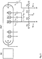
- the PMT has a cathode K, an anode AN, and a plurality of dynodes DN arranged in a tube 10.
- the plurality of dynodes form a chain towards the anode, each dynode corresponding ta a stage of amplification of the PMT.
- the voltage divider circuitry which applies an acceleration voltage to each dynode of the dynode chain, the acceleration voltage for the respective dynode increasing towards the anode.
- the scintillator SC (if any) in front of the cathode of the PMT.
- the read-out circuitry of the already known embodiment of Fig. 1 comprises a fully differential operation amplifier (pamp).
- a fully differential opamp is designed to provide a pair of synchronous AC output voltage signals U A + out , U A - out whereby the one output voltage signal has an inverse form of the other one.
- Such signals are also denoted as differential signals.
- the output signals may be shifted by DC voltages (bias or offset voltages) such has they have always only one polarity, e.g., positive.
- the respective offset voltage has to be greater or equal to one halve of the maximum negative swing (amplitude) U MAX of the respective signal.
- the offset voltage is the common mode voltage level V CM .
- the common mode voltage level V CM is set by clamping the center input of the differential opamp to that voltage.
- both output signals U A + out , U A - out have always the same polarity (e.g., positive)
- the one signal may still be called the inverted signal of the other one, and the signals are still called differential signals.
- the electrical charge flow i A from the PMT's anode is applied via a capacitive element C A to a load resistance R LOAD , and flows then to ground.
- the voltage across R LOAD is captured by the opamp.
- the fully differential opamp provides at its outputs two synchronous signals over time, the first being representative of the charge flow at the anode, the second output signal having an inverted form thereof.
- U MAX being the maximum amplitude of the voltage across R LOAD ., i.e., the voltage to be captured by the opamp, and U CENTER being the common mode signal level V CM .
- Fig. 2 illustrates an embodiment of the invention.
- the PMT is connected to a circuitry that produces the differential output signal pair.
- the PMT may be the same one as described with Fig. 1 above. But here, both differential signals are taken from the PMT directly.
- the dynode signal almost exactly mirrors the anode signal with a small delay of one to e.g., three nanoseconds.
- the dynode signal has the opposite polarity and at a different magnitude than the anode.
- the respective signal is made of the difference of the incoming electrons minus the outgoing multiplied electrons.
- the readout circuitry is implemented with passive elements only.
- Anode AN of the PMT is connected to a differential input node A + of the circuitry, and the upper dynode(s) is/are connected to differential input node A - of the circuitry.
- Anode and dynode(s) are AC-coupled by capacitors C A , C DN , C DN-1 , C DN-2 ...with the readout circuitry. Behind the decoupling they are connected to two different voltage divider resistor networks, i.e., first and second sub-circuitry, respectively.
- a - is attached to the sub-circuitry consisting of resistor elements R AH and R AL
- a + is attached to the sub-circuitry consisting of resistor elements R DH and R DL .
- the charge flow from the anode is i A
- the polarity of the current i A and i D are inverted to each other and may have different amplitudes (i.e., swing).
- the resistors networks have two functions.
- the first function is a current to voltage conversion matching the desired ADC input range.
- the second function is maintaining a desired common mode DC voltage level.
- V DD shall be an arbitrary voltage source which is larger than the maximum voltage U MAX that could be supplied to either node A + and A - .
- V CM denotes the targeted common mode voltage level.
- U MAX denotes the maximum targeted voltage swing of the output voltage.
- I MAX denotes the targeted current flowing from the anode at which the full differential voltage swing is reached.
- the anode load R AG : (R DH ⁇ R AL ) / (R AH + R AL ) is the total resistance of the network at the anode.
- the dynode load R DG : (R DH ⁇ R DL ) / (R DH + R DL ) is similarly given at the dynode.
- the maximum differential voltage swing shall be achieved.
- the 4 equations can be resolved for the resistor networks delivering values for R AL , R AH , R DL , and R DH .
- the afore mentioned ratio of 3 ⁇ 4 can be greatly improved to almost unity.
- the two last dynodes would give a ratio of 15/16, the three last dynodes 63/64, the four last dynodes 255/256, and so on.
- the four resistor elements may have the following values:
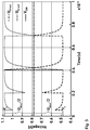
- Fig. 3 illustrates typical output signals U A + out , U A - out and common mode voltage V CM at the respective output terminals A + and A - .
- the AC portions of U A + out , and U A - out are a differential signal pair. That means, the AC portion of the one signal is an inverted form of the other signal, i.e., the signals they are symmetrical with respect to the common mode voltage V CM , which is the center voltage U CENTER .
Landscapes
- Physics & Mathematics (AREA)
- Health & Medical Sciences (AREA)
- Life Sciences & Earth Sciences (AREA)
- General Physics & Mathematics (AREA)
- High Energy & Nuclear Physics (AREA)
- Molecular Biology (AREA)
- Spectroscopy & Molecular Physics (AREA)
- Measurement Of Radiation (AREA)
Claims (15)
- Ausleseschaltung für eine Photovervielfacherröhre (PMT), die zum Liefern eines Paares von ersten und zweiten synchronen Ausgangssignalen (UA + out, UA - out) angepasst ist, wobei das erste Ausgangssignal (UA + out) des Paares einen ersten Wechselstromanteil aufweist, der typisch für einen Ladungsfluss einer Anode (AN) der PMT mit der Zeit ist, wobei das zweite Ausgangssignal (UA - out) des Paares einen zweiten Wechselstromanteil aufweist, der einer invertierten Form des ersten Wechselstromanteils des ersten Ausgangssignals (UA + out) entspricht, wobei die Ausleseschaltung Folgendes umfasst:eine erste Teilschaltung (RAH, RAL), die angepasst ist, das erste Ausgangssignal (UA + out) aus dem Ladungsfluss mit der Zeit (iA) der Anode (AN) abzuleiten, undeine zweite Teilschaltung (RDH + RDL), die angepasst ist, das zweite Ausgangssignal (UA - out) aus einem Ladungsfluss mit der Zeit (io) von mindestens einer Dynode (DN, DN-1, DN-2,...) der PMT abzuleiten,wobei das erste Ausgangssignal ferner einen ersten Gleichstromanteil (UCENTER + UMAX / 2) umfasst und das zweite Ausgangssignal ferner einen zweiten Gleichstromanteil (UCENTER - UMAX / 2) umfasst,
wobei die erste Teilschaltung eine erste Spannungsquellenschaltung (VDD) zum Einstellen des ersten Gleichstromanteils des ersten Ausgangssignals (UA + out) umfasst, und wobei die zweite Teilschaltung eine zweite Spannungsquellenschaltung (VDD) zum Einstellen des zweiten Gleichstromanteils des zweiten Ausgangssignals (UA - out) umfasst,
wobei die erste Teilschaltung ein erstes und ein zweites Widerstandselement zum Einstellen des Gleichstromanteils des ersten Ausgangssignals (UA + out) umfasst, und wobei die zweite Teilschaltung ein drittes und ein viertes Widerstandselement zum Einstellen des Gleichstromanteils der zweiten Ausgangsspannung (UA - out) umfasst.
wobei das erste und das zweite Widerstandselement zwischen der ersten Spannungsquelle und einem Massepotential in Reihe geschaltet sind und einen gemeinsamen ersten Anschlusspunkt des ersten und des zweiten Widerstandselements definieren, wobei das erste Widerstandselement an Masse angeschlossen ist und das zweite Widerstandselement an der ersten Spannungsquelle angeschlossen ist,
wobei der erste Anschlusspunkt das erste Ausgangssignal bereitstellt und ferner mit der Anode wechselstromverbindbar ist,
wobei das dritte und das vierte Widerstandselement zwischen der zweiten Spannungsquelle und dem Massepotential in Reihe geschaltet sind,
und einen gemeinsamen zweiten Anschlusspunkt des dritten und des vierten Widerstandselements definieren,
wobei das dritte Widerstandselement an Masse angeschlossen ist, und das vierte Widerstandselement an der zweiten Spannungsquelle angeschlossen ist,
wobei der zweite Anschlusspunkt das zweite Ausgangssignal bereitstellt und ferner mit der mindestens einen Dynode wechselstromverbindbar ist,
wobei die erste Teilschaltung und die zweite Teilschaltung nur aus passiven Elementen bestehen. - Ausleseschaltung nach Anspruch 1, wobei der erste Wechselstromanteil und der zweite Wechselstromanteil ein Paar von Differenzsignalen ausbilden.
- Ausleseschaltung nach Anspruch 1 oder 2, wobei die erste Teilschaltung mit der Anode (AN) wechselstromverbindbar ist, und die zweite Teilschaltung mit der mindestens einen Dynode (DN, DN-1, DN-2,...) wechselstromverbindbar ist.
- Ausleseschaltung nach dem vorhergehenden Anspruch, wobei das erste Widerstandselement, das RAL ist, das zweite Widerstandselement, das RAH ist, das dritte Widerstandselement, das RDL ist, und das vierte Widerstandselement, das RDH ist, die folgenden Bedingungen für maximal eine Ausgangsspannung, Vh, und minimal eine andere Spannung, V1, bei maximalem Ladungsfluss von der Anode mit der Zeit erfüllen:


 VDD der Spannungspegel der ersten und der zweiten Spannungsquelle ist,VCM der Mittelwert der Ausgangsspannungen ist,UMAX ein zuvor bestimmter maximaler Spannungshub ist,
 Gdyn der Stromverstärkungsfaktor der mindestens einen Dynode ist.IMAX dem maximalen Ladungsfluss von der Anode mit der Zeit entspricht.
 - Ausleseschaltung nach einem der vorhergehenden Ansprüche, wobei der Ladungsfluss mit der Zeit von mindestens einer Dynodenladung basierend auf der der Anode am nächsten liegenden einen Dynode bestimmt wird.
- Ausleseschaltung nach einem der vorhergehenden Ansprüche, wobei der Ladungsfluss mit der Zeit von mindestens einer Dynodenladung basierend auf mindestens einer der Dynoden neben der der Anode am nächsten liegenden einen Dynode bestimmt wird.
- Ausleseschaltung nach einem der vorhergehenden Ansprüche, wobei die erste Teilschaltung über ein Kondensatorelement (CA) mit der Anode (AN) wechselstromverbindbar ist und die zweite Teilschaltung über mindestens ein Kondensatorelement (CDN, CDN-1, CDN-2,....) mit der mindestens einen Dynode (DN, DN-1, DN-2,...) wechselstromverbindbar ist.
- PMT, die eine Kathode (CA), eine Anode (AN) und mehrere Dynoden (DN, DN-1, DN-2,...) für die Messung von Kernstrahlung, vorzugsweise Gammastrahlung, aufweist, die mindestens eine Ausleseschaltung nach einem der vorhergehenden Ansprüche umfasst.
- Szintillationsdetektorvorrichtung (SC), die mindestens eine PMT nach den vorhergehenden Ansprüchen und einen Abtast-ADC umfasst.
- Verfahren zum Auslesen eines Paares von ersten und zweiten synchronen Ausgangssignalen (UA + out, UA - out) aus einer Photovervielfacherröhre (PMT) mittels der Ausleseschaltung nach einem der Ansprüche 1 bis 7,
wobei das erste Ausgangssignal (UA + out) des Paars einen ersten Wechselstromanteil aufweist, der typisch für einen Ladungsfluss einer Anode (AN) der PMT mit der Zeit ist, wobei das zweite Ausgangssignal (UA - out) des Paars einen zweiten Wechselstromanteil aufweist, der einer invertierten Form des ersten Wechselstromanteils des ersten Ausgangssignals (UA + out) entspricht, wobei der erste Wechselstromanteil und der zweite Wechselstromanteil ein Paar von Differenzsignalen ausbilden, wobei das Verfahren zu Folgendem angepasst ist:Ableiten des ersten Ausgangssignal (UA + out) aus dem Ladungsfluss mit der Zeit (iA) der Anode (AN), undAbleiten des zweiten Ausgangssignals (UA - out) aus einem Ladungsfluss mit der Zeit (iD) von mindestens einer Dynode (DN, DN-1, DN-2,...) der PMT,wobei das erste Ausgangssignal ferner einen ersten Gleichstromanteil (UCENTER + UMAX / 2) umfasst und das zweite Ausgangssignal ferner einen zweiten Gleichstromanteil (UCENTER - UMAX / 2) umfasst,
Einstellen des ersten Gleichstromanteils des ersten Ausgangssignals (UA + out) durch Anlegen einer ersten Spannung (VDD) an die erste Teilschaltung, und Einstellen des zweiten Gleichstromanteils des zweiten Ausgangssignals (UA - out) durch Anlegen einer zweiten Spannung (VDD) an die zweite Teilschaltung. - Verfahren nach dem vorhergehenden Anspruch, wobei der erste Wechselstromanteil und der zweite Wechselstromanteil ein Paar von Differenzsignalen ausbilden.
- Verfahren nach Anspruch 10 oder 11, wobei die erste Teilschaltung mit der Anode (AN) wechselstromverbindbar ist, und die zweite Teilschaltung mit der mindestens einen Dynode (DN, DN-1, DN-2,...) wechselstromverbindbar ist.
- Verfahren nach einem der Ansprüche 10 bis 12, das ferner das Wechselstromverbinden der ersten Teilschaltung mit der Anode (AN) über ein Kondensatorelement (CA), und das Wechselstromverbinden der zweiten Teilschaltung mit der mindestens einen Dynode (DN, DN-1, DN-2,...) über mindestens ein Kondensatorelement (CDN, CDN-1, CDN-2,....) umfasst.
- Verfahren nach einem der Ansprüche 10 bis 13, das ferner Folgendes umfasst:Wechselstromverbinden der Anode (AN) mit der ersten Teilschaltung über ein Kondensatorelement (CA), undWechselstromverbinden einer Dynode der mindestens einen Dynode (DN, DN-1, DN-2,...) mit der zweiten Teilschaltung über mindestens ein weiteres Kondensatorelement (CDN, CDN-1, CDN-2,....).
- Verfahren nach einem der Ansprüche 10 bis 14, das ferner Folgendes umfasst:
Umwandeln der Ausgangssignale in digitale Signale.
Applications Claiming Priority (1)
| Application Number | Priority Date | Filing Date | Title |
|---|---|---|---|
| PCT/EP2015/074282 WO2017067582A1 (en) | 2015-10-20 | 2015-10-20 | Readout circuitry for photomultiplier and photomultiplier |
Publications (2)
| Publication Number | Publication Date |
|---|---|
| EP3365705A1 EP3365705A1 (de) | 2018-08-29 |
| EP3365705B1 true EP3365705B1 (de) | 2020-09-16 |
Family
ID=54345484
Family Applications (1)
| Application Number | Title | Priority Date | Filing Date |
|---|---|---|---|
| EP15784340.0A Active EP3365705B1 (de) | 2015-10-20 | 2015-10-20 | Ausleseschaltung für photonenvervielfacher und photonenvervielfacher |
Country Status (3)
| Country | Link |
|---|---|
| US (1) | US10520612B2 (de) |
| EP (1) | EP3365705B1 (de) |
| WO (1) | WO2017067582A1 (de) |
Families Citing this family (3)
| Publication number | Priority date | Publication date | Assignee | Title |
|---|---|---|---|---|
| WO2021175427A1 (en) | 2020-03-05 | 2021-09-10 | Target Systemelektronik Gmbh & Co. Kg | Method for determining the neutron flux by using a portable radionuclide identification device (rid) comprising scintillation material with iodine |
| EP4562413A1 (de) | 2022-07-26 | 2025-06-04 | Rapiscan Holdings, Inc. | Verfahren und systeme zur durchführung von sofortigen automatischen kalibrierungseinstellungen von röntgeninspektionssystemen |
| CN119087497B (zh) * | 2024-09-25 | 2025-09-23 | 湖北方圆科学仪器股份有限公司 | 一种液体闪烁谱仪能谱探测信号处理方法及装置 |
Family Cites Families (4)
| Publication number | Priority date | Publication date | Assignee | Title |
|---|---|---|---|---|
| US4820914A (en) * | 1988-01-20 | 1989-04-11 | Vigyan Research Associates, Inc. | Gain control of photomultiplier tubes used in detecting differential absorption lidar returns |
| US7414715B2 (en) * | 2005-07-14 | 2008-08-19 | Kla-Tencor Technologies Corp. | Systems, circuits and methods for extending the detection range of an inspection system by avoiding detector saturation |
| US10074528B2 (en) * | 2010-12-17 | 2018-09-11 | Thermo Fisher Scientific (Bremen) Gmbh | Data acquisition system and method for mass spectrometry |
| JP6301138B2 (ja) * | 2013-02-12 | 2018-03-28 | キヤノンメディカルシステムズ株式会社 | X線コンピュータ断層撮影装置およびフォトンカウンティングプログラム |
-
2015
- 2015-10-20 WO PCT/EP2015/074282 patent/WO2017067582A1/en not_active Ceased
- 2015-10-20 EP EP15784340.0A patent/EP3365705B1/de active Active
-
2018
- 2018-04-20 US US15/958,085 patent/US10520612B2/en active Active
Non-Patent Citations (1)
| Title |
|---|
| None * |
Also Published As
| Publication number | Publication date |
|---|---|
| WO2017067582A1 (en) | 2017-04-27 |
| EP3365705A1 (de) | 2018-08-29 |
| US20180239035A1 (en) | 2018-08-23 |
| US10520612B2 (en) | 2019-12-31 |
Similar Documents
| Publication | Publication Date | Title |
|---|---|---|
| US10809395B2 (en) | Photon measurement front-end circuit with integral module and a negative feedback module | |
| US5754056A (en) | Charge detector with long integration time | |
| Popov et al. | Analog readout system with charge division type output | |
| CN105765405B (zh) | 用于探测光子的探测设备和其方法 | |
| Popov et al. | Readout electronics for multianode photomultiplier tubes with pad matrix anode layout | |
| US10520612B2 (en) | Readout circuitry for photomultiplier and photomultiplier | |
| US11635531B2 (en) | Apparatus for measuring photon information and photon measurement device | |
| JPWO2012077218A1 (ja) | 放射線検出器 | |
| JPH06283983A (ja) | パルス光受信回路 | |
| US8525094B2 (en) | Photoelectric conversion circuit | |
| US11139293B2 (en) | Photon detector | |
| US6317070B1 (en) | Floating-point analog-to-digital converter | |
| WO2021027447A1 (zh) | 辐射探测装置和成像系统 | |
| Dey et al. | A row-column summing readout architecture for SiPM based PET imaging systems | |
| US9361485B2 (en) | Transmission device and sensor system | |
| EP3399345B1 (de) | Lesenetzwerktopologie | |
| US12149246B2 (en) | Circuit arrangement and method for charge integration | |
| Heifets et al. | Fully active voltage divider for PMT photo-detector | |
| CN110118600B (zh) | 信号处理电路和包括该信号处理电路的光电探测系统 | |
| JP4727511B2 (ja) | 高速アナログ/ディジタルコンバータ | |
| US11887829B2 (en) | Ion detector current converter | |
| CN114762252A (zh) | 峰值检测器电路和用于评估第一输入电压的峰值的方法 | |
| CN223078480U (zh) | 具有增益补偿的能量测量电路 | |
| US12196898B2 (en) | Signal processing system and method for radiation detector based on metal oxide semiconductor (MOS) transistor | |
| CN118655612A (zh) | 具有增益补偿的能量测量电路及增益补偿方法 |
Legal Events
| Date | Code | Title | Description |
|---|---|---|---|
| STAA | Information on the status of an ep patent application or granted ep patent |
Free format text: STATUS: THE INTERNATIONAL PUBLICATION HAS BEEN MADE |
|
| PUAI | Public reference made under article 153(3) epc to a published international application that has entered the european phase |
Free format text: ORIGINAL CODE: 0009012 |
|
| STAA | Information on the status of an ep patent application or granted ep patent |
Free format text: STATUS: REQUEST FOR EXAMINATION WAS MADE |
|
| 17P | Request for examination filed |
Effective date: 20180522 |
|
| AK | Designated contracting states |
Kind code of ref document: A1 Designated state(s): AL AT BE BG CH CY CZ DE DK EE ES FI FR GB GR HR HU IE IS IT LI LT LU LV MC MK MT NL NO PL PT RO RS SE SI SK SM TR |
|
| AX | Request for extension of the european patent |
Extension state: BA ME |
|
| DAV | Request for validation of the european patent (deleted) | ||
| DAX | Request for extension of the european patent (deleted) | ||
| GRAP | Despatch of communication of intention to grant a patent |
Free format text: ORIGINAL CODE: EPIDOSNIGR1 |
|
| STAA | Information on the status of an ep patent application or granted ep patent |
Free format text: STATUS: GRANT OF PATENT IS INTENDED |
|
| INTG | Intention to grant announced |
Effective date: 20200409 |
|
| GRAS | Grant fee paid |
Free format text: ORIGINAL CODE: EPIDOSNIGR3 |
|
| GRAA | (expected) grant |
Free format text: ORIGINAL CODE: 0009210 |
|
| STAA | Information on the status of an ep patent application or granted ep patent |
Free format text: STATUS: THE PATENT HAS BEEN GRANTED |
|
| AK | Designated contracting states |
Kind code of ref document: B1 Designated state(s): AL AT BE BG CH CY CZ DE DK EE ES FI FR GB GR HR HU IE IS IT LI LT LU LV MC MK MT NL NO PL PT RO RS SE SI SK SM TR |
|
| REG | Reference to a national code |
Ref country code: GB Ref legal event code: FG4D |
|
| REG | Reference to a national code |
Ref country code: CH Ref legal event code: EP |
|
| REG | Reference to a national code |
Ref country code: DE Ref legal event code: R096 Ref document number: 602015059207 Country of ref document: DE |
|
| REG | Reference to a national code |
Ref country code: IE Ref legal event code: FG4D |
|
| REG | Reference to a national code |
Ref country code: AT Ref legal event code: REF Ref document number: 1314655 Country of ref document: AT Kind code of ref document: T Effective date: 20201015 |
|
| PG25 | Lapsed in a contracting state [announced via postgrant information from national office to epo] |
Ref country code: FI Free format text: LAPSE BECAUSE OF FAILURE TO SUBMIT A TRANSLATION OF THE DESCRIPTION OR TO PAY THE FEE WITHIN THE PRESCRIBED TIME-LIMIT Effective date: 20200916 Ref country code: HR Free format text: LAPSE BECAUSE OF FAILURE TO SUBMIT A TRANSLATION OF THE DESCRIPTION OR TO PAY THE FEE WITHIN THE PRESCRIBED TIME-LIMIT Effective date: 20200916 Ref country code: SE Free format text: LAPSE BECAUSE OF FAILURE TO SUBMIT A TRANSLATION OF THE DESCRIPTION OR TO PAY THE FEE WITHIN THE PRESCRIBED TIME-LIMIT Effective date: 20200916 Ref country code: NO Free format text: LAPSE BECAUSE OF FAILURE TO SUBMIT A TRANSLATION OF THE DESCRIPTION OR TO PAY THE FEE WITHIN THE PRESCRIBED TIME-LIMIT Effective date: 20201216 Ref country code: GR Free format text: LAPSE BECAUSE OF FAILURE TO SUBMIT A TRANSLATION OF THE DESCRIPTION OR TO PAY THE FEE WITHIN THE PRESCRIBED TIME-LIMIT Effective date: 20201217 Ref country code: BG Free format text: LAPSE BECAUSE OF FAILURE TO SUBMIT A TRANSLATION OF THE DESCRIPTION OR TO PAY THE FEE WITHIN THE PRESCRIBED TIME-LIMIT Effective date: 20201216 |
|
| REG | Reference to a national code |
Ref country code: AT Ref legal event code: MK05 Ref document number: 1314655 Country of ref document: AT Kind code of ref document: T Effective date: 20200916 |
|
| REG | Reference to a national code |
Ref country code: NL Ref legal event code: MP Effective date: 20200916 |
|
| PG25 | Lapsed in a contracting state [announced via postgrant information from national office to epo] |
Ref country code: LV Free format text: LAPSE BECAUSE OF FAILURE TO SUBMIT A TRANSLATION OF THE DESCRIPTION OR TO PAY THE FEE WITHIN THE PRESCRIBED TIME-LIMIT Effective date: 20200916 Ref country code: RS Free format text: LAPSE BECAUSE OF FAILURE TO SUBMIT A TRANSLATION OF THE DESCRIPTION OR TO PAY THE FEE WITHIN THE PRESCRIBED TIME-LIMIT Effective date: 20200916 |
|
| REG | Reference to a national code |
Ref country code: LT Ref legal event code: MG4D |
|
| PG25 | Lapsed in a contracting state [announced via postgrant information from national office to epo] |
Ref country code: LT Free format text: LAPSE BECAUSE OF FAILURE TO SUBMIT A TRANSLATION OF THE DESCRIPTION OR TO PAY THE FEE WITHIN THE PRESCRIBED TIME-LIMIT Effective date: 20200916 Ref country code: EE Free format text: LAPSE BECAUSE OF FAILURE TO SUBMIT A TRANSLATION OF THE DESCRIPTION OR TO PAY THE FEE WITHIN THE PRESCRIBED TIME-LIMIT Effective date: 20200916 Ref country code: RO Free format text: LAPSE BECAUSE OF FAILURE TO SUBMIT A TRANSLATION OF THE DESCRIPTION OR TO PAY THE FEE WITHIN THE PRESCRIBED TIME-LIMIT Effective date: 20200916 Ref country code: PT Free format text: LAPSE BECAUSE OF FAILURE TO SUBMIT A TRANSLATION OF THE DESCRIPTION OR TO PAY THE FEE WITHIN THE PRESCRIBED TIME-LIMIT Effective date: 20210118 Ref country code: SM Free format text: LAPSE BECAUSE OF FAILURE TO SUBMIT A TRANSLATION OF THE DESCRIPTION OR TO PAY THE FEE WITHIN THE PRESCRIBED TIME-LIMIT Effective date: 20200916 Ref country code: CZ Free format text: LAPSE BECAUSE OF FAILURE TO SUBMIT A TRANSLATION OF THE DESCRIPTION OR TO PAY THE FEE WITHIN THE PRESCRIBED TIME-LIMIT Effective date: 20200916 |
|
| PG25 | Lapsed in a contracting state [announced via postgrant information from national office to epo] |
Ref country code: ES Free format text: LAPSE BECAUSE OF FAILURE TO SUBMIT A TRANSLATION OF THE DESCRIPTION OR TO PAY THE FEE WITHIN THE PRESCRIBED TIME-LIMIT Effective date: 20200916 Ref country code: AT Free format text: LAPSE BECAUSE OF FAILURE TO SUBMIT A TRANSLATION OF THE DESCRIPTION OR TO PAY THE FEE WITHIN THE PRESCRIBED TIME-LIMIT Effective date: 20200916 Ref country code: AL Free format text: LAPSE BECAUSE OF FAILURE TO SUBMIT A TRANSLATION OF THE DESCRIPTION OR TO PAY THE FEE WITHIN THE PRESCRIBED TIME-LIMIT Effective date: 20200916 Ref country code: PL Free format text: LAPSE BECAUSE OF FAILURE TO SUBMIT A TRANSLATION OF THE DESCRIPTION OR TO PAY THE FEE WITHIN THE PRESCRIBED TIME-LIMIT Effective date: 20200916 Ref country code: IS Free format text: LAPSE BECAUSE OF FAILURE TO SUBMIT A TRANSLATION OF THE DESCRIPTION OR TO PAY THE FEE WITHIN THE PRESCRIBED TIME-LIMIT Effective date: 20210116 |
|
| REG | Reference to a national code |
Ref country code: CH Ref legal event code: PL |
|
| REG | Reference to a national code |
Ref country code: DE Ref legal event code: R097 Ref document number: 602015059207 Country of ref document: DE |
|
| PG25 | Lapsed in a contracting state [announced via postgrant information from national office to epo] |
Ref country code: MC Free format text: LAPSE BECAUSE OF FAILURE TO SUBMIT A TRANSLATION OF THE DESCRIPTION OR TO PAY THE FEE WITHIN THE PRESCRIBED TIME-LIMIT Effective date: 20200916 Ref country code: LU Free format text: LAPSE BECAUSE OF NON-PAYMENT OF DUE FEES Effective date: 20201020 Ref country code: SK Free format text: LAPSE BECAUSE OF FAILURE TO SUBMIT A TRANSLATION OF THE DESCRIPTION OR TO PAY THE FEE WITHIN THE PRESCRIBED TIME-LIMIT Effective date: 20200916 |
|
| REG | Reference to a national code |
Ref country code: BE Ref legal event code: MM Effective date: 20201031 |
|
| PLBE | No opposition filed within time limit |
Free format text: ORIGINAL CODE: 0009261 |
|
| STAA | Information on the status of an ep patent application or granted ep patent |
Free format text: STATUS: NO OPPOSITION FILED WITHIN TIME LIMIT |
|
| 26N | No opposition filed |
Effective date: 20210617 |
|
| PG25 | Lapsed in a contracting state [announced via postgrant information from national office to epo] |
Ref country code: BE Free format text: LAPSE BECAUSE OF NON-PAYMENT OF DUE FEES Effective date: 20201031 Ref country code: CH Free format text: LAPSE BECAUSE OF NON-PAYMENT OF DUE FEES Effective date: 20201031 Ref country code: DK Free format text: LAPSE BECAUSE OF FAILURE TO SUBMIT A TRANSLATION OF THE DESCRIPTION OR TO PAY THE FEE WITHIN THE PRESCRIBED TIME-LIMIT Effective date: 20200916 Ref country code: SI Free format text: LAPSE BECAUSE OF FAILURE TO SUBMIT A TRANSLATION OF THE DESCRIPTION OR TO PAY THE FEE WITHIN THE PRESCRIBED TIME-LIMIT Effective date: 20200916 Ref country code: LI Free format text: LAPSE BECAUSE OF NON-PAYMENT OF DUE FEES Effective date: 20201031 |
|
| PG25 | Lapsed in a contracting state [announced via postgrant information from national office to epo] |
Ref country code: IT Free format text: LAPSE BECAUSE OF FAILURE TO SUBMIT A TRANSLATION OF THE DESCRIPTION OR TO PAY THE FEE WITHIN THE PRESCRIBED TIME-LIMIT Effective date: 20200916 Ref country code: IE Free format text: LAPSE BECAUSE OF NON-PAYMENT OF DUE FEES Effective date: 20201020 |
|
| PG25 | Lapsed in a contracting state [announced via postgrant information from national office to epo] |
Ref country code: TR Free format text: LAPSE BECAUSE OF FAILURE TO SUBMIT A TRANSLATION OF THE DESCRIPTION OR TO PAY THE FEE WITHIN THE PRESCRIBED TIME-LIMIT Effective date: 20200916 Ref country code: MT Free format text: LAPSE BECAUSE OF FAILURE TO SUBMIT A TRANSLATION OF THE DESCRIPTION OR TO PAY THE FEE WITHIN THE PRESCRIBED TIME-LIMIT Effective date: 20200916 Ref country code: CY Free format text: LAPSE BECAUSE OF FAILURE TO SUBMIT A TRANSLATION OF THE DESCRIPTION OR TO PAY THE FEE WITHIN THE PRESCRIBED TIME-LIMIT Effective date: 20200916 |
|
| PG25 | Lapsed in a contracting state [announced via postgrant information from national office to epo] |
Ref country code: MK Free format text: LAPSE BECAUSE OF FAILURE TO SUBMIT A TRANSLATION OF THE DESCRIPTION OR TO PAY THE FEE WITHIN THE PRESCRIBED TIME-LIMIT Effective date: 20200916 |
|
| PG25 | Lapsed in a contracting state [announced via postgrant information from national office to epo] |
Ref country code: NL Free format text: LAPSE BECAUSE OF NON-PAYMENT OF DUE FEES Effective date: 20200923 |
|
| REG | Reference to a national code |
Ref country code: DE Ref legal event code: R082 Ref document number: 602015059207 Country of ref document: DE Representative=s name: MURGITROYD GERMANY PATENTANWALTSGESELLSCHAFT M, DE |
|
| PGFP | Annual fee paid to national office [announced via postgrant information from national office to epo] |
Ref country code: DE Payment date: 20241029 Year of fee payment: 10 |
|
| PGFP | Annual fee paid to national office [announced via postgrant information from national office to epo] |
Ref country code: GB Payment date: 20241030 Year of fee payment: 10 |
|
| PGFP | Annual fee paid to national office [announced via postgrant information from national office to epo] |
Ref country code: FR Payment date: 20241029 Year of fee payment: 10 |
|
| REG | Reference to a national code |
Ref country code: DE Ref legal event code: R081 Ref document number: 602015059207 Country of ref document: DE Owner name: RAPISCAN HOLDINGS, INC., WILMINGTON, US Free format text: FORMER OWNER: TARGET SYSTEMELEKTRONIK GMBH & CO. KG, 42287 WUPPERTAL, DE |
|
| REG | Reference to a national code |
Ref country code: GB Ref legal event code: 732E Free format text: REGISTERED BETWEEN 20251120 AND 20251126 |