EP3361614A1 - High side driver without dedicated supply in high voltage applications - Google Patents
High side driver without dedicated supply in high voltage applications Download PDFInfo
- Publication number
- EP3361614A1 EP3361614A1 EP18154189.7A EP18154189A EP3361614A1 EP 3361614 A1 EP3361614 A1 EP 3361614A1 EP 18154189 A EP18154189 A EP 18154189A EP 3361614 A1 EP3361614 A1 EP 3361614A1
- Authority
- EP
- European Patent Office
- Prior art keywords
- highside
- lowside
- switch
- terminal
- pin
- Prior art date
- Legal status (The legal status is an assumption and is not a legal conclusion. Google has not performed a legal analysis and makes no representation as to the accuracy of the status listed.)
- Withdrawn
Links
Images

Classifications
-
- H—ELECTRICITY
- H02—GENERATION; CONVERSION OR DISTRIBUTION OF ELECTRIC POWER
- H02M—APPARATUS FOR CONVERSION BETWEEN AC AND AC, BETWEEN AC AND DC, OR BETWEEN DC AND DC, AND FOR USE WITH MAINS OR SIMILAR POWER SUPPLY SYSTEMS; CONVERSION OF DC OR AC INPUT POWER INTO SURGE OUTPUT POWER; CONTROL OR REGULATION THEREOF
- H02M3/00—Conversion of DC power input into DC power output
- H02M3/02—Conversion of DC power input into DC power output without intermediate conversion into AC
- H02M3/04—Conversion of DC power input into DC power output without intermediate conversion into AC by static converters
- H02M3/10—Conversion of DC power input into DC power output without intermediate conversion into AC by static converters using discharge tubes with control electrode or semiconductor devices with control electrode
- H02M3/145—Conversion of DC power input into DC power output without intermediate conversion into AC by static converters using discharge tubes with control electrode or semiconductor devices with control electrode using devices of a triode or transistor type requiring continuous application of a control signal
- H02M3/155—Conversion of DC power input into DC power output without intermediate conversion into AC by static converters using discharge tubes with control electrode or semiconductor devices with control electrode using devices of a triode or transistor type requiring continuous application of a control signal using semiconductor devices only
- H02M3/156—Conversion of DC power input into DC power output without intermediate conversion into AC by static converters using discharge tubes with control electrode or semiconductor devices with control electrode using devices of a triode or transistor type requiring continuous application of a control signal using semiconductor devices only with automatic control of output voltage or current, e.g. switching regulators
- H02M3/158—Conversion of DC power input into DC power output without intermediate conversion into AC by static converters using discharge tubes with control electrode or semiconductor devices with control electrode using devices of a triode or transistor type requiring continuous application of a control signal using semiconductor devices only with automatic control of output voltage or current, e.g. switching regulators including plural semiconductor devices as final control devices for a single load
-
- H—ELECTRICITY
- H02—GENERATION; CONVERSION OR DISTRIBUTION OF ELECTRIC POWER
- H02M—APPARATUS FOR CONVERSION BETWEEN AC AND AC, BETWEEN AC AND DC, OR BETWEEN DC AND DC, AND FOR USE WITH MAINS OR SIMILAR POWER SUPPLY SYSTEMS; CONVERSION OF DC OR AC INPUT POWER INTO SURGE OUTPUT POWER; CONTROL OR REGULATION THEREOF
- H02M3/00—Conversion of DC power input into DC power output
- H02M3/02—Conversion of DC power input into DC power output without intermediate conversion into AC
- H02M3/04—Conversion of DC power input into DC power output without intermediate conversion into AC by static converters
- H02M3/10—Conversion of DC power input into DC power output without intermediate conversion into AC by static converters using discharge tubes with control electrode or semiconductor devices with control electrode
- H02M3/145—Conversion of DC power input into DC power output without intermediate conversion into AC by static converters using discharge tubes with control electrode or semiconductor devices with control electrode using devices of a triode or transistor type requiring continuous application of a control signal
- H02M3/155—Conversion of DC power input into DC power output without intermediate conversion into AC by static converters using discharge tubes with control electrode or semiconductor devices with control electrode using devices of a triode or transistor type requiring continuous application of a control signal using semiconductor devices only
- H02M3/156—Conversion of DC power input into DC power output without intermediate conversion into AC by static converters using discharge tubes with control electrode or semiconductor devices with control electrode using devices of a triode or transistor type requiring continuous application of a control signal using semiconductor devices only with automatic control of output voltage or current, e.g. switching regulators
- H02M3/158—Conversion of DC power input into DC power output without intermediate conversion into AC by static converters using discharge tubes with control electrode or semiconductor devices with control electrode using devices of a triode or transistor type requiring continuous application of a control signal using semiconductor devices only with automatic control of output voltage or current, e.g. switching regulators including plural semiconductor devices as final control devices for a single load
- H02M3/1588—Conversion of DC power input into DC power output without intermediate conversion into AC by static converters using discharge tubes with control electrode or semiconductor devices with control electrode using devices of a triode or transistor type requiring continuous application of a control signal using semiconductor devices only with automatic control of output voltage or current, e.g. switching regulators including plural semiconductor devices as final control devices for a single load comprising at least one synchronous rectifier element
-
- H—ELECTRICITY
- H02—GENERATION; CONVERSION OR DISTRIBUTION OF ELECTRIC POWER
- H02M—APPARATUS FOR CONVERSION BETWEEN AC AND AC, BETWEEN AC AND DC, OR BETWEEN DC AND DC, AND FOR USE WITH MAINS OR SIMILAR POWER SUPPLY SYSTEMS; CONVERSION OF DC OR AC INPUT POWER INTO SURGE OUTPUT POWER; CONTROL OR REGULATION THEREOF
- H02M3/00—Conversion of DC power input into DC power output
- H02M3/02—Conversion of DC power input into DC power output without intermediate conversion into AC
- H02M3/04—Conversion of DC power input into DC power output without intermediate conversion into AC by static converters
- H02M3/10—Conversion of DC power input into DC power output without intermediate conversion into AC by static converters using discharge tubes with control electrode or semiconductor devices with control electrode
- H02M3/145—Conversion of DC power input into DC power output without intermediate conversion into AC by static converters using discharge tubes with control electrode or semiconductor devices with control electrode using devices of a triode or transistor type requiring continuous application of a control signal
- H02M3/155—Conversion of DC power input into DC power output without intermediate conversion into AC by static converters using discharge tubes with control electrode or semiconductor devices with control electrode using devices of a triode or transistor type requiring continuous application of a control signal using semiconductor devices only
- H02M3/156—Conversion of DC power input into DC power output without intermediate conversion into AC by static converters using discharge tubes with control electrode or semiconductor devices with control electrode using devices of a triode or transistor type requiring continuous application of a control signal using semiconductor devices only with automatic control of output voltage or current, e.g. switching regulators
-
- H—ELECTRICITY
- H03—ELECTRONIC CIRCUITRY
- H03K—PULSE TECHNIQUE
- H03K17/00—Electronic switching or gating, i.e. not by contact-making and –breaking
- H03K17/06—Modifications for ensuring a fully conducting state
- H03K17/063—Modifications for ensuring a fully conducting state in field-effect transistor switches
-
- H—ELECTRICITY
- H02—GENERATION; CONVERSION OR DISTRIBUTION OF ELECTRIC POWER
- H02M—APPARATUS FOR CONVERSION BETWEEN AC AND AC, BETWEEN AC AND DC, OR BETWEEN DC AND DC, AND FOR USE WITH MAINS OR SIMILAR POWER SUPPLY SYSTEMS; CONVERSION OF DC OR AC INPUT POWER INTO SURGE OUTPUT POWER; CONTROL OR REGULATION THEREOF
- H02M1/00—Details of apparatus for conversion
- H02M1/0003—Details of control, feedback or regulation circuits
- H02M1/0006—Arrangements for supplying an adequate voltage to the control circuit of converters
-
- H—ELECTRICITY
- H03—ELECTRONIC CIRCUITRY
- H03K—PULSE TECHNIQUE
- H03K19/00—Logic circuits, i.e. having at least two inputs acting on one output; Inverting circuits
- H03K19/01—Modifications for accelerating switching
- H03K19/017—Modifications for accelerating switching in field-effect transistor circuits
- H03K19/01707—Modifications for accelerating switching in field-effect transistor circuits in asynchronous circuits
- H03K19/01714—Modifications for accelerating switching in field-effect transistor circuits in asynchronous circuits by bootstrapping, i.e. by positive feed-back
-
- H—ELECTRICITY
- H03—ELECTRONIC CIRCUITRY
- H03K—PULSE TECHNIQUE
- H03K2217/00—Indexing scheme related to electronic switching or gating, i.e. not by contact-making or -breaking covered by H03K17/00
- H03K2217/0045—Full bridges, determining the direction of the current through the load
-
- H—ELECTRICITY
- H03—ELECTRONIC CIRCUITRY
- H03K—PULSE TECHNIQUE
- H03K2217/00—Indexing scheme related to electronic switching or gating, i.e. not by contact-making or -breaking covered by H03K17/00
- H03K2217/0063—High side switches, i.e. the higher potential [DC] or life wire [AC] being directly connected to the switch and not via the load
-
- H—ELECTRICITY
- H03—ELECTRONIC CIRCUITRY
- H03K—PULSE TECHNIQUE
- H03K2217/00—Indexing scheme related to electronic switching or gating, i.e. not by contact-making or -breaking covered by H03K17/00
- H03K2217/0072—Low side switches, i.e. the lower potential [DC] or neutral wire [AC] being directly connected to the switch and not via the load
-
- H—ELECTRICITY
- H03—ELECTRONIC CIRCUITRY
- H03K—PULSE TECHNIQUE
- H03K2217/00—Indexing scheme related to electronic switching or gating, i.e. not by contact-making or -breaking covered by H03K17/00
- H03K2217/0081—Power supply means, e.g. to the switch driver
-
- Y—GENERAL TAGGING OF NEW TECHNOLOGICAL DEVELOPMENTS; GENERAL TAGGING OF CROSS-SECTIONAL TECHNOLOGIES SPANNING OVER SEVERAL SECTIONS OF THE IPC; TECHNICAL SUBJECTS COVERED BY FORMER USPC CROSS-REFERENCE ART COLLECTIONS [XRACs] AND DIGESTS
- Y02—TECHNOLOGIES OR APPLICATIONS FOR MITIGATION OR ADAPTATION AGAINST CLIMATE CHANGE
- Y02B—CLIMATE CHANGE MITIGATION TECHNOLOGIES RELATED TO BUILDINGS, e.g. HOUSING, HOUSE APPLIANCES OR RELATED END-USER APPLICATIONS
- Y02B70/00—Technologies for an efficient end-user side electric power management and consumption
- Y02B70/10—Technologies improving the efficiency by using switched-mode power supplies [SMPS], i.e. efficient power electronics conversion e.g. power factor correction or reduction of losses in power supplies or efficient standby modes
Definitions
- This disclosure relates to DC-DC power converters.
- a DC-to-DC power converter typically steps down voltage while stepping up current, from its input supply to its output load. It is a class of switched-mode power supply (SMPS) typically containing at least two semiconductors (a diode and a transistor, although modern buck converters frequently replace the diode with a second transistor used for synchronous rectification) and at least one energy storage element, a capacitor, inductor, or the two in combination. To reduce voltage ripple, filters made of capacitors (sometimes in combination with inductors) are normally added to such a converter's output and input. Switching converters provide much greater power efficiency as DC-to-DC converters than linear regulators, which are simpler circuits that lower voltages by dissipating power as heat, but do not step up output current.
- SMPS switched-mode power supply
- topologies there are several topologies in a power supply application.
- a well-known topology is the buck converter.
- Other topologies such as resonant, flyback or forward converter are also used.
- Some topologies use a low side as well as a high side switch.
- the disadvantage of a high side switch is that it requires a dedicated supply.
- a bootstrap supply circuitry consisting of a diode and a capacitor, may be used. This circuitry needs to be supplied from a supply which output voltage is sufficient to drive the external MOSFET (typical minimum voltage 8V), but must always remain below the maximum drive voltage of the external MOSFET (typically 20V). As this voltage is not always available in a typical power supply, it needs to be either provided by the control IC or derived from a dedicated circuitry.
- a dedicated circuitry is the additional components, which goes at the cost of area (form factor) and costs. For this reason, several control integrated circuits (IC's) provide a dedicated supply via a dedicated pin. However, the form factor of a power supply must be minimized to such that even the pin count of a control IC must be minimized. Which then also reduces the cost even further.
- a DC-to-DC converter in one embodiment, includes a highside switch having a first terminal, a second terminal and a gate. The first terminal is coupled to an input voltage terminal.
- the SMPS driver further includes a lowside switch having a first terminal, a second terminal and a gate. The first terminal of the lowside switch is coupled to the second terminal of the highside switch and the second terminal of the lowside switch is coupled to ground.
- a diode is coupled to the gate of the lowside switch on one side and to a capacitor on the other side.
- An integrated circuit (IC) is included to generate control signals for switching the highside switch and the lowside switch.
- the IC includes a highside supply pin, a highside gate control pin, a half bridge pin, a lowside gate control pin and a ground pin.
- the gate of the lowside switch is coupled to the lowside gate control pin
- the highside supply pin is coupled to the diode
- the capacitor is coupled to the half bridge pin.
- the IC includes a first driver that is coupled to the highside gate control pin, the half bridge pin and the highside supply.
- the first driver is controlled by a binary control signal that cause the first driver to couple the half bridge pin or the highside supply pin to the highside gate control pin.
- the IC also includes a second driver that is coupled to the lowside gate control pin, a switch voltage line and the ground pin.
- the second driver is controlled by a binary control signal that cause the second driver to couple the ground pin or the switch voltage line to the lowside gate control pin.
- the switch voltage line is configured to carry a switching voltage that is lower than the voltage at the input voltage terminal.
- the input voltage terminal is configured to accept up to 400V.
- the highside switch and the lowside switch are switchable through a voltage in the range of 8V to 20V.
- the DC-to-DC converter described above may be used in high voltage circuits such as switch mode power supplies (SMPS).
- SMPS switch mode power supplies
- high voltage means a voltage that is higher than a switching voltage range of the highside or lowside switch described above.
- a DC-to-DC converter in yet another embodiment, includes two highside switches, each having a first terminal, a second terminal and a gate, wherein the first terminal is coupled to an input voltage terminal.
- the DC-to-DC converter also includes two lowside switches, each having a first terminal, a second terminal and a gate, wherein the first terminal of the lowside switch is coupled to the second terminal of the highside switch and the second terminal of the lowside switch is coupled to ground.
- Two diodes are included, each coupled to the gate of one of the lowside switches on one side and to a capacitor on the other side.
- the DC-to-DC converter also includes an integrated circuit (IC) to generate control signals for switching each of the highside switches and each of the lowside switches.
- IC integrated circuit
- the IC includes two highside supply pins, two highside gate control pins, two half bridge pins, two lowside gate control pins and a ground pin, wherein the gate of the each of the lowside switches is coupled to one of the lowside gate control pins, one of the highside supply pins is coupled to one of the diodes and the capacitor is coupled to one of the half bridge pins.
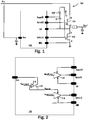
- FIG. 1 depicts a schematic circuit diagram 100 of a DC-to-DC converter including a high side driver without a need for a dedicated additional PIN in a driver integrated circuit (IC) 102 for providing dedicated supply for driving a high side switch 104.
- the highside MOSFET 104 is driven by a bootstrap supply including a diode 108 and a capacitor C1.
- the lowside MOSFET 106 is driven by the GateLS signal and the highside MOSFET 104 is driven by the GateHS signal.
- the GateLS driver is supplied between ground (GND) and the Vswitch voltage.
- Vswitch may be 8V to 20V, but may also depends on the characteristics of MOSFETs 104, 106.
- the lowside MOSFET 106 When Vin is within Vswitch lower and upper ranges, the lowside MOSFET 106 may be driven by Vin itself. Also, the highside MOSFET 104 can be driven through SuppHS by connecting the diode 108 directly to Vin. However, when Vin is higher than the upper range of Vswitch, one end of the diode 108 is coupled to the GateLS PIN which is coupled to the gate of the lowside MOSFET 108. It may be noted that Vin may range from 20V to 400V. It may be noted that to limit the current I d through the diode 108, a resistor (not shown) may be place in series.
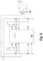
- a full bridge topology will include two circuits 100 where the output of one circuit coupled to one end of an inductor 122 and the output of the other circuit coupled to the other end of the inductor 122.
- a driver IC 120 includes two driver sides, each identical to a driver side of the IC 102 to driver each other of the two half bridge circuits
- the voltage at the HB (Half Bridge) PIN is approximately zero volt because HB is connected to GND through the lowside MOSFET 106.
- Vswitch the voltage at the GateLS PIN
- the highside MOSFET 104 is turned “on” through the voltage at the GateHS PIN (that is same as the voltage at the SuppHS PIN to turn the highside MOSFET 104 "on”).
- the SuppHS PIN supplied by the charge stored in the capacitor C1.
- the capacitor C1 is discharged when the capacitor C1 provides voltage to drive the highside MOSFET 104.
- the voltage at HB (V BH ) becomes low (or zero).
- the capacitor C1 is charged again when the GateLS goes high.
- a separate driver supply is not needed for driving the highside MOSFET 104.
- a Vout terminal is coupled to the source of the highside MOSFET 104 through an inductor L and a capacitor. Vout is typically linear DC voltage with minimum ripples.
- FIG. 2 depicts a schematic circuit inside the driver IC 102. It should be noted many components inside the IC 102 are not being shown so as not to obscure the present disclosure.
- the IC 102 includes a driver 112 that couples either SuppHS or V HB to GateHS PIN depending on whether the driver signal GateHS_dlg is high or low.
- the IC 102 also includes another driver 114 that couples the GateLS pin to either the Vswitch line or the GND PIN depending on whether the signal GateLS_dlg is high or low.
- a comparator 116 drives a switch 110 to generate Vswitch from the input Vcc or Vin.
- Vswitchref is a reference voltage equal to the voltage Vswitch.
- Vswitchref is selected within the switching voltage range of the high and lowside MOSFETs 104, 106. Switching voltage is measured between the gate and the source of MOSFETs and this is a voltage difference between the gate and the source that is capable of turning MOSFET "on". It should be noted that Vswitch is in the range of the lower and upper switching voltages of the lowside MOSFET 106 and the highside MOSFET 104.
- Control signals GateHS_dlg and GateLS_dlg are generated by a control circuit (not shown) in the IC 102. When GateHS_dlg is high, GateLS_dlg is low and vice versa.
- Figure 3 depicts outputs graphs of the circuit 100.
- Graph A shows the current I d through the diode 108.
- the current I d spikes occur when the voltage at HB PIN goes down to zero when the lowerside MOSFET 106 is on.
- the width of the current spike in graph A corresponds to the charging time of the capacitor C1.
- the capacitor C1 When the capacitor C1 is fully charged, the current I d goes to zero (or substantially zero) and the capacitor C1 has voltage Vswitch across it.
- the HB voltage is equal to Vin, as depicted in the graph B, and the GateHS voltage is V HB + Vswitch (the capacitor C1 voltage on top of V HB ), as depicted in the graph C. Therefore, the voltage between the gate and the source of the higherside MOSFET 104 is Vswitch.
- the voltage at the GateLS PIN switches between Vswitch and zero, as depicted in the graph D.
- the circuit 100 is therefore suitable for a wide range of Vin without making design changes or changing the lowerside MOSFET 106 and the higherside MOSFET 104 because Vswitch is independent of Vin.
- the SMPS driver includes a highside switch having a first terminal, a second terminal and a gate. The first terminal is coupled to an input voltage terminal.
- the SMPS driver further includes a lowside switch having a first terminal, a second terminal and a gate. The first terminal of the lowside switch is coupled to the second terminal of the highside switch and the second terminal of the lowside switch is coupled to ground.
- a diode is coupled to the gate of the lowside switch on one side and to a capacitor on the other side.
- An integrated circuit (IC) is included to generate control signals for switching the highside switch and the lowside switch.
- the IC includes a highside supply pin, a highside gate control pin, a half bridge pin, a lowside gate control pin and a ground pin.
- the gate of the lowside switch is coupled to the lowside gate control pin
- the highside supply pin is coupled to the diode
- the capacitor is coupled to the half bridge pin.
Landscapes
- Engineering & Computer Science (AREA)
- Power Engineering (AREA)
- Dc-Dc Converters (AREA)
Abstract
A DC-to-DC converter is disclosed. The SMPS driver includes a highside switch having a first terminal, a second terminal and a gate. The first terminal is coupled to an input voltage terminal. The SMPS driver further includes a lowside switch having a first terminal, a second terminal and a gate. The first terminal of the lowside switch is coupled to the second terminal of the highside switch and the second terminal of the lowside switch is coupled to ground. A diode is coupled to the gate of the lowside switch on one side and to a capacitor on the other side. An integrated circuit (IC) is included to generate control signals for switching the highside switch and the lowside switch. The IC includes a highside supply pin, a highside gate control pin, a half bridge pin, a lowside gate control pin and a ground pin. The gate of the lowside switch is coupled to the lowside gate control pin, the highside supply pin is coupled to the diode and the capacitor is coupled to the half bridge pin.
Description
- This disclosure relates to DC-DC power converters.
- A DC-to-DC power converter typically steps down voltage while stepping up current, from its input supply to its output load. It is a class of switched-mode power supply (SMPS) typically containing at least two semiconductors (a diode and a transistor, although modern buck converters frequently replace the diode with a second transistor used for synchronous rectification) and at least one energy storage element, a capacitor, inductor, or the two in combination. To reduce voltage ripple, filters made of capacitors (sometimes in combination with inductors) are normally added to such a converter's output and input. Switching converters provide much greater power efficiency as DC-to-DC converters than linear regulators, which are simpler circuits that lower voltages by dissipating power as heat, but do not step up output current.
- There are several topologies in a power supply application. A well-known topology is the buck converter. Other topologies such as resonant, flyback or forward converter are also used. Some topologies use a low side as well as a high side switch. The disadvantage of a high side switch is that it requires a dedicated supply. For the dedicated supply, a bootstrap supply circuitry, consisting of a diode and a capacitor, may be used. This circuitry needs to be supplied from a supply which output voltage is sufficient to drive the external MOSFET (typical minimum voltage 8V), but must always remain below the maximum drive voltage of the external MOSFET (typically 20V). As this voltage is not always available in a typical power supply, it needs to be either provided by the control IC or derived from a dedicated circuitry.
- The disadvantage of a dedicated circuitry is the additional components, which goes at the cost of area (form factor) and costs. For this reason, several control integrated circuits (IC's) provide a dedicated supply via a dedicated pin. However, the form factor of a power supply must be minimized to such that even the pin count of a control IC must be minimized. Which then also reduces the cost even further.
- This Summary is provided to introduce a selection of concepts in a simplified form that are further described below in the Detailed Description. This Summary is not intended to identify key features or essential features of the claimed subject matter, nor is it intended to be used to limit the scope of the claimed subject matter.
- In one embodiment, a DC-to-DC converter is disclosed. The SMPS driver includes a highside switch having a first terminal, a second terminal and a gate. The first terminal is coupled to an input voltage terminal. The SMPS driver further includes a lowside switch having a first terminal, a second terminal and a gate. The first terminal of the lowside switch is coupled to the second terminal of the highside switch and the second terminal of the lowside switch is coupled to ground. A diode is coupled to the gate of the lowside switch on one side and to a capacitor on the other side. An integrated circuit (IC) is included to generate control signals for switching the highside switch and the lowside switch. The IC includes a highside supply pin, a highside gate control pin, a half bridge pin, a lowside gate control pin and a ground pin. The gate of the lowside switch is coupled to the lowside gate control pin, the highside supply pin is coupled to the diode and the capacitor is coupled to the half bridge pin.
- In some embodiments, the IC includes a first driver that is coupled to the highside gate control pin, the half bridge pin and the highside supply. The first driver is controlled by a binary control signal that cause the first driver to couple the half bridge pin or the highside supply pin to the highside gate control pin. The IC also includes a second driver that is coupled to the lowside gate control pin, a switch voltage line and the ground pin. The second driver is controlled by a binary control signal that cause the second driver to couple the ground pin or the switch voltage line to the lowside gate control pin. The switch voltage line is configured to carry a switching voltage that is lower than the voltage at the input voltage terminal.
- In some embodiments, the input voltage terminal is configured to accept up to 400V. The highside switch and the lowside switch are switchable through a voltage in the range of 8V to 20V. The DC-to-DC converter described above may be used in high voltage circuits such as switch mode power supplies (SMPS). As used herein the term "high voltage" means a voltage that is higher than a switching voltage range of the highside or lowside switch described above.
- In yet another embodiment, a DC-to-DC converter is disclosed. The DC-to-DC converter includes two highside switches, each having a first terminal, a second terminal and a gate, wherein the first terminal is coupled to an input voltage terminal. The DC-to-DC converter also includes two lowside switches, each having a first terminal, a second terminal and a gate, wherein the first terminal of the lowside switch is coupled to the second terminal of the highside switch and the second terminal of the lowside switch is coupled to ground. Two diodes are included, each coupled to the gate of one of the lowside switches on one side and to a capacitor on the other side. The DC-to-DC converter also includes an integrated circuit (IC) to generate control signals for switching each of the highside switches and each of the lowside switches. The IC includes two highside supply pins, two highside gate control pins, two half bridge pins, two lowside gate control pins and a ground pin, wherein the gate of the each of the lowside switches is coupled to one of the lowside gate control pins, one of the highside supply pins is coupled to one of the diodes and the capacitor is coupled to one of the half bridge pins.
- So that the manner in which the above recited features of the present invention can be understood in detail, a more particular description of the invention, briefly summarized above, may be had by reference to embodiments, some of which are illustrated in the appended drawings. It is to be noted, however, that the appended drawings illustrate only typical embodiments of this invention and are therefore not to be considered limiting of its scope, for the invention may admit to other equally effective embodiments. Advantages of the subject matter claimed will become apparent to those skilled in the art upon reading this description in conjunction with the accompanying drawings, in which like reference numerals have been used to designate like elements, and in which:
-
FIG. 1 depicts a schematic circuit diagram of a DC-to-DC converter including a high side driver without a need for a dedicated additional PIN in a driver integrated circuit (IC) for providing dedicated supply for driving a high side transistor in accordance with one or more embodiments of the present disclosure; -
FIG. 2 depicts a schematic circuit inside the driver IC in accordance with one or more embodiments of the present disclosure; and -
FIG. 3 depicts output graphs the high side driver circuit ofFIG. 1 . -
FIG. 4 depicts a DC-to-DC converter in a full bridge topology using substantially two copies of the circuit depicted inFIG. 1 . - Note that figures are not drawn to scale. Intermediate steps between figure transitions have been omitted so as not to obfuscate the disclosure. Those intermediate steps are known to a person skilled in the art.
- Many well-known manufacturing steps, components, and connectors have been omitted or not described in details in the description so as not to obfuscate the present disclosure.
-
Figure 1 depicts a schematic circuit diagram 100 of a DC-to-DC converter including a high side driver without a need for a dedicated additional PIN in a driver integrated circuit (IC) 102 for providing dedicated supply for driving ahigh side switch 104. Thehighside MOSFET 104 is driven by a bootstrap supply including adiode 108 and a capacitor C1. Thelowside MOSFET 106 is driven by the GateLS signal and thehighside MOSFET 104 is driven by the GateHS signal. The GateLS driver is supplied between ground (GND) and the Vswitch voltage. Typically, Vswitch may be 8V to 20V, but may also depends on the characteristics ofMOSFETs lowside MOSFET 106 may be driven by Vin itself. Also, thehighside MOSFET 104 can be driven through SuppHS by connecting thediode 108 directly to Vin. However, when Vin is higher than the upper range of Vswitch, one end of thediode 108 is coupled to the GateLS PIN which is coupled to the gate of thelowside MOSFET 108. It may be noted that Vin may range from 20V to 400V. It may be noted that to limit the current Id through thediode 108, a resistor (not shown) may be place in series. - It should be noted that even though the embodiments herein are described in context of a half bridge topology, a person skilled in the art would appreciate that these embodiments may also be equally applicable to a full bridge topology of DC-to-DC converters. As shown in
Figure 4 , a full bridge topology will include twocircuits 100 where the output of one circuit coupled to one end of aninductor 122 and the output of the other circuit coupled to the other end of theinductor 122. Adriver IC 120 includes two driver sides, each identical to a driver side of theIC 102 to driver each other of the two half bridge circuits - When the
lowside MOSFET 106 is "on", the voltage at the HB (Half Bridge) PIN is approximately zero volt because HB is connected to GND through thelowside MOSFET 106. When the voltage at HB is zero the capacitor C1 is charged to Vswitch (the voltage at the GateLS PIN) via thediode 108. When the lowside MOSFET 106 (the voltage at the GateLS PIN is zero) is "off' and thehighside MOSFET 104 is turned "on" through the voltage at the GateHS PIN (that is same as the voltage at the SuppHS PIN to turn thehighside MOSFET 104 "on"). The SuppHS PIN supplied by the charge stored in the capacitor C1. The capacitor C1 is discharged when the capacitor C1 provides voltage to drive thehighside MOSFET 104. When the GateHS is low again, the voltage at HB (VBH) becomes low (or zero). The capacitor C1 is charged again when the GateLS goes high. As apparent, a separate driver supply is not needed for driving thehighside MOSFET 104. A Vout terminal is coupled to the source of thehighside MOSFET 104 through an inductor L and a capacitor. Vout is typically linear DC voltage with minimum ripples. -
Figure 2 depicts a schematic circuit inside thedriver IC 102. It should be noted many components inside theIC 102 are not being shown so as not to obscure the present disclosure. TheIC 102 includes adriver 112 that couples either SuppHS or VHB to GateHS PIN depending on whether the driver signal GateHS_dlg is high or low. TheIC 102 also includes anotherdriver 114 that couples the GateLS pin to either the Vswitch line or the GND PIN depending on whether the signal GateLS_dlg is high or low. Acomparator 116 drives aswitch 110 to generate Vswitch from the input Vcc or Vin. Vswitchref is a reference voltage equal to the voltage Vswitch. Vswitchref is selected within the switching voltage range of the high andlowside MOSFETs lowside MOSFET 106 and thehighside MOSFET 104. Control signals GateHS_dlg and GateLS_dlg are generated by a control circuit (not shown) in theIC 102. When GateHS_dlg is high, GateLS_dlg is low and vice versa. -
Figure 3 depicts outputs graphs of thecircuit 100. Graph A shows the current Id through thediode 108. The current Id spikes occur when the voltage at HB PIN goes down to zero when thelowerside MOSFET 106 is on. The width of the current spike in graph A corresponds to the charging time of the capacitor C1. When the capacitor C1 is fully charged, the current Id goes to zero (or substantially zero) and the capacitor C1 has voltage Vswitch across it. When thehigherside MOSFET 104 is "on" and thelowerside MOSFER 106 is "off", the HB voltage is equal to Vin, as depicted in the graph B, and the GateHS voltage is VHB + Vswitch (the capacitor C1 voltage on top of VHB), as depicted in the graph C. Therefore, the voltage between the gate and the source of thehigherside MOSFET 104 is Vswitch. The voltage at the GateLS PIN switches between Vswitch and zero, as depicted in the graph D. - The
circuit 100 is therefore suitable for a wide range of Vin without making design changes or changing thelowerside MOSFET 106 and thehigherside MOSFET 104 because Vswitch is independent of Vin. - A DC-to-DC converter is disclosed. The SMPS driver includes a highside switch having a first terminal, a second terminal and a gate. The first terminal is coupled to an input voltage terminal. The SMPS driver further includes a lowside switch having a first terminal, a second terminal and a gate. The first terminal of the lowside switch is coupled to the second terminal of the highside switch and the second terminal of the lowside switch is coupled to ground. A diode is coupled to the gate of the lowside switch on one side and to a capacitor on the other side. An integrated circuit (IC) is included to generate control signals for switching the highside switch and the lowside switch. The IC includes a highside supply pin, a highside gate control pin, a half bridge pin, a lowside gate control pin and a ground pin. The gate of the lowside switch is coupled to the lowside gate control pin, the highside supply pin is coupled to the diode and the capacitor is coupled to the half bridge pin.
- Some or all of these embodiments may be combined, some may be omitted altogether, and additional process steps can be added while still achieving the products described herein. Thus, the subject matter described herein can be embodied in many different variations, and all such variations are contemplated to be within the scope of what is claimed.
- While one or more implementations have been described by way of example and in terms of the specific embodiments, it is to be understood that one or more implementations are not limited to the disclosed embodiments. To the contrary, it is intended to cover various modifications and similar arrangements as would be apparent to those skilled in the art. Therefore, the scope of the appended claims should be accorded the broadest interpretation so as to encompass all such modifications and similar arrangements.
- The use of the terms "a" and "an" and "the" and similar referents in the context of describing the subject matter (particularly in the context of the following claims) are to be construed to cover both the singular and the plural, unless otherwise indicated herein or clearly contradicted by context. Recitation of ranges of values herein are merely intended to serve as a shorthand method of referring individually to each separate value falling within the range, unless otherwise indicated herein, and each separate value is incorporated into the specification as if it were individually recited herein. Furthermore, the foregoing description is for the purpose of illustration only, and not for the purpose of limitation, as the scope of protection sought is defined by the claims as set forth hereinafter together with any equivalents thereof entitled to. The use of any and all examples, or exemplary language (e.g., "such as") provided herein, is intended merely to better illustrate the subject matter and does not pose a limitation on the scope of the subject matter unless otherwise claimed. The use of the term "based on" and other like phrases indicating a condition for bringing about a result, both in the claims and in the written description, is not intended to foreclose any other conditions that bring about that result. No language in the specification should be construed as indicating any non-claimed element as essential to the practice of the invention as claimed.
- Preferred embodiments are described herein, including the best mode known to the inventor for carrying out the claimed subject matter. Of course, variations of those preferred embodiments will become apparent to those of ordinary skill in the art upon reading the foregoing description. The inventor expects skilled artisans to employ such variations as appropriate, and the inventor intends for the claimed subject matter to be practiced otherwise than as specifically described herein. Accordingly, this claimed subject matter includes all modifications and equivalents of the subject matter recited in the claims appended hereto as permitted by applicable law. Moreover, any combination of the above-described elements in all possible variations thereof is encompassed unless otherwise indicated herein or otherwise clearly contradicted by context.
Claims (15)
- A DC-to-DC converter, comprising:a highside switch having a first terminal, a second terminal and a gate, wherein the first terminal is coupled to an input voltage terminal;a lowside switch having a first terminal, a second terminal and a gate, wherein the first terminal of the lowside switch is coupled to the second terminal of the highside switch and the second terminal of the lowside switch is coupled to ground;a diode coupled to the gate of the lowside switch on one side and to a capacitor on the other side; andan integrated circuit (IC) to generate control signals for switching the highside switch and the lowside switch, wherein the IC includes a highside supply pin, a highside gate control pin, a half bridge pin, a lowside gate control pin and a ground pin, wherein the gate of the lowside switch is coupled to the lowside gate control pin, the highside supply pin is coupled to the diode and the capacitor is coupled to the half bridge pin.
- The DC-to-DC converter of claim 1, wherein the IC includes a first driver that is coupled to the highside gate control pin, the half bridge pin and the highside supply pin.
- The DC-to-DC converter of claim 2, wherein the first driver is controlled by a binary control signal that cause the first driver to couple the half bridge pin or the highside supply pin to the highside gate control pin.
- The DC-to-DC converter of any preceding claim, wherein the IC includes a second driver that is coupled to the lowside gate control pin, a switch voltage line and the ground pin.
- The DC-to-DC converter of claim 4, wherein the second driver is controlled by a binary control signal that cause the second driver to couple the ground pin or the switch voltage line to the lowside gate control pin.
- The DC-to-DC converter of claim 4 or 5, wherein the switch voltage line is configured to carry a switching voltage that is lower than the voltage at the input voltage terminal.
- The DC-to-DC converter of any preceding claim, wherein the input voltage terminal is configured to accept up to 400V.
- The DC-to-DC converter of any preceding claim, wherein the highside switch and the lowside switch are switchable through a voltage in the range of 8V to 20V.
- A switch mode power supply (SMPS) comprising the DC-to-DC converter of any preceding claim.
- A DC-to-DC converter according to claim 1, further comprising:a second highside switch having a first terminal, a second terminal and a gate, whereinthe first terminal is coupled to an input voltage terminal;a second lowside switch having a first terminal, a second terminal and a gate, wherein the first terminal of the second lowside switch is coupled to the second terminal of the second highside switch and the second terminal of the second lowside switch is coupled to ground;a second diode coupled to the gate of the second lowside switch on one side and to a second capacitor on the other side; and wherein theintegrated circuit (IC) is further configured to generate control signals for switching each of the highside switches and each of the lowside switches, wherein the IC includes two highside supply pins, two highside gate control pins, two half bridge pins, two lowside gate control pins and a ground pin, wherein the gate of the each of the lowside switches is coupled to one of the lowside gate control pins, one of the highside supply pins is coupled to one of the diodes and one of the capacitors is coupled to one of the half bridge pins.
- The DC-to-DC converter of claim 10, wherein the IC includes a first driver that is coupled to one of the highside gate control pins, one of the half bridge pins and one of the highside supply pins.
- The DC-to-DC converter of claim 10 or 11, wherein the first driver is controlled by a binary control signal that causes the first driver to couple one of the half bridge pins or one of the highside supply pins to one of the highside gate control pins.
- The DC-to-DC converter of any of claims 10 to 12, wherein the IC includes a second driver that is coupled to one the lowside gate control pins, a switch voltage line and the ground pin.
- The DC-to-DC converter of claim 13, wherein the second driver is controlled by a binary control signal that cause the second driver to couple the ground pin or the switch voltage line to one of the lowside gate control pins.
- The DC-to-DC converter of any of claims 10 to 14, wherein the highside switches and the lowside switches are switchable through a voltage in the range of 8V to 20V.
Applications Claiming Priority (1)
| Application Number | Priority Date | Filing Date | Title |
|---|---|---|---|
| US15/432,797 US10103629B2 (en) | 2017-02-14 | 2017-02-14 | High side driver without dedicated supply in high voltage applications |
Publications (1)
| Publication Number | Publication Date |
|---|---|
| EP3361614A1 true EP3361614A1 (en) | 2018-08-15 |
Family
ID=61094340
Family Applications (1)
| Application Number | Title | Priority Date | Filing Date |
|---|---|---|---|
| EP18154189.7A Withdrawn EP3361614A1 (en) | 2017-02-14 | 2018-01-30 | High side driver without dedicated supply in high voltage applications |
Country Status (2)
| Country | Link |
|---|---|
| US (1) | US10103629B2 (en) |
| EP (1) | EP3361614A1 (en) |
Families Citing this family (1)
| Publication number | Priority date | Publication date | Assignee | Title |
|---|---|---|---|---|
| CN207603443U (en) * | 2017-09-21 | 2018-07-10 | 北京比特大陆科技有限公司 | It calculates power plate power stage circuit, packaging power device and calculates power plate |
Citations (3)
| Publication number | Priority date | Publication date | Assignee | Title |
|---|---|---|---|---|
| US20050102128A1 (en) * | 2003-11-12 | 2005-05-12 | International Rectifier Corporation | Bootstrap diode emulator with dynamic back-gate biasing |
| KR20100108073A (en) * | 2009-03-27 | 2010-10-06 | 단국대학교 산학협력단 | Level shifter using bootstrap capacitor, inverter having the same, and level shifting method thereof |
| US20140021932A1 (en) * | 2012-07-19 | 2014-01-23 | Jens Ejury | Charge Recovery in Power Converter Driver Stages |
Family Cites Families (13)
| Publication number | Priority date | Publication date | Assignee | Title |
|---|---|---|---|---|
| US6963498B2 (en) * | 2004-02-02 | 2005-11-08 | International Rectifier Corporation | Bootstrap capacitor refresh circuit |
| US7106105B2 (en) * | 2004-07-21 | 2006-09-12 | Fairchild Semiconductor Corporation | High voltage integrated circuit driver with a high voltage PMOS bootstrap diode emulator |
| EP1776000A3 (en) * | 2005-10-12 | 2008-05-28 | Int Rectifier Corp | 8-Pin PFC and ballast control IC |
| JP2009512165A (en) * | 2005-10-12 | 2009-03-19 | インターナショナル レクティファイアー コーポレイション | Dimming ballast control integrated circuit |
| KR100687936B1 (en) * | 2005-11-29 | 2007-02-27 | 삼성전자주식회사 | Electronic device and power circuit |
| EP2087587B1 (en) * | 2006-10-20 | 2018-12-19 | Nxp B.V. | Power amplifier |
| US7466185B2 (en) * | 2006-10-23 | 2008-12-16 | Infineon Technologies Ag | IGBT-Driver circuit for desaturated turn-off with high desaturation level |
| TW201218631A (en) | 2010-10-19 | 2012-05-01 | Analog Integrations Corp | Bootstrap circuit without a regulator and a diode |
| US8558584B2 (en) * | 2010-11-30 | 2013-10-15 | Infineon Technologies Ag | System and method for bootstrapping a switch driver |
| TWI485410B (en) * | 2012-12-03 | 2015-05-21 | Anpec Electronics Corp | Bootstrap capacitor detecting circuit and bootstrap dc-dc converter thereof |
| TWI463776B (en) * | 2012-12-06 | 2014-12-01 | Anpec Electronics Corp | Bootstrap dc-dc converter |
| CN104716815B (en) * | 2013-12-16 | 2018-09-04 | 台达电子企业管理(上海)有限公司 | Power Circuit and Power System |
| US9667245B2 (en) * | 2014-10-10 | 2017-05-30 | Efficient Power Conversion Corporation | High voltage zero QRR bootstrap supply |
-
2017
- 2017-02-14 US US15/432,797 patent/US10103629B2/en active Active
-
2018
- 2018-01-30 EP EP18154189.7A patent/EP3361614A1/en not_active Withdrawn
Patent Citations (3)
| Publication number | Priority date | Publication date | Assignee | Title |
|---|---|---|---|---|
| US20050102128A1 (en) * | 2003-11-12 | 2005-05-12 | International Rectifier Corporation | Bootstrap diode emulator with dynamic back-gate biasing |
| KR20100108073A (en) * | 2009-03-27 | 2010-10-06 | 단국대학교 산학협력단 | Level shifter using bootstrap capacitor, inverter having the same, and level shifting method thereof |
| US20140021932A1 (en) * | 2012-07-19 | 2014-01-23 | Jens Ejury | Charge Recovery in Power Converter Driver Stages |
Also Published As
| Publication number | Publication date |
|---|---|
| US20180234015A1 (en) | 2018-08-16 |
| US10103629B2 (en) | 2018-10-16 |
Similar Documents
| Publication | Publication Date | Title |
|---|---|---|
| CN106664020B (en) | Shared Bootstrap Capacitors and Methods for Multiphase Buck Converter Circuits | |
| US9780661B2 (en) | High efficiency DC-DC converter with active shunt to accommodate high input voltage transients | |
| US8994411B2 (en) | System and method for bootstrapping a switch driver | |
| CN100454737C (en) | Switching regulator, power supply circuit including the same, and auxiliary battery charging circuit | |
| CN104767360B (en) | System and method for driving switch | |
| EP2136462A1 (en) | DC-DC Converter | |
| US7245087B2 (en) | Power conversion device | |
| CN102480216B (en) | System and method for driving acascode switch | |
| JP2014180087A (en) | Step-up switching regulator and semiconductor device | |
| CN116131586B (en) | A power converter and a switch control circuit | |
| US20250070645A1 (en) | Gate drive circuit, power good circuit, overcurrent detection circuit, oscillation prevention circuit, switching control circuit and switching power supply device | |
| US7304463B2 (en) | DC-DC converter | |
| WO2019187544A1 (en) | Power factor improvement circuit and semiconductor device | |
| WO2020024111A1 (en) | Voltage supply for synchronous rectifier controller during low voltage output conditions | |
| EP1879284B1 (en) | DC-DC converter and power supply apparatus | |
| US20130285628A1 (en) | Integrated Power Supply with Wide Input Supply Voltage Range | |
| US7054168B1 (en) | Undershoot eliminator circuit and method for synchronous rectified DC-DC converters | |
| JP2021010286A (en) | Drive circuit | |
| US10770984B2 (en) | Switching control device with reverse bias circuit | |
| EP3361614A1 (en) | High side driver without dedicated supply in high voltage applications | |
| US12003180B2 (en) | Power supply for driving synchronous rectification elements of SEPIC converter | |
| JP2006191706A (en) | Dc converter | |
| CN117411292A (en) | Integrated circuits, power circuits | |
| JP4997984B2 (en) | Synchronous rectification type DC-DC converter. | |
| JP4609285B2 (en) | Semiconductor integrated circuit for power supply and power supply device |
Legal Events
| Date | Code | Title | Description |
|---|---|---|---|
| PUAI | Public reference made under article 153(3) epc to a published international application that has entered the european phase |
Free format text: ORIGINAL CODE: 0009012 |
|
| STAA | Information on the status of an ep patent application or granted ep patent |
Free format text: STATUS: THE APPLICATION HAS BEEN PUBLISHED |
|
| AK | Designated contracting states |
Kind code of ref document: A1 Designated state(s): AL AT BE BG CH CY CZ DE DK EE ES FI FR GB GR HR HU IE IS IT LI LT LU LV MC MK MT NL NO PL PT RO RS SE SI SK SM TR |
|
| AX | Request for extension of the european patent |
Extension state: BA ME |
|
| STAA | Information on the status of an ep patent application or granted ep patent |
Free format text: STATUS: THE APPLICATION IS DEEMED TO BE WITHDRAWN |
|
| 18D | Application deemed to be withdrawn |
Effective date: 20190216 |