EP3361295A2 - Optical polarizing filter - Google Patents
Optical polarizing filter Download PDFInfo
- Publication number
- EP3361295A2 EP3361295A2 EP18153121.1A EP18153121A EP3361295A2 EP 3361295 A2 EP3361295 A2 EP 3361295A2 EP 18153121 A EP18153121 A EP 18153121A EP 3361295 A2 EP3361295 A2 EP 3361295A2
- Authority
- EP
- European Patent Office
- Prior art keywords
- layers
- approximately
- refractive index
- polarization
- optical
- Prior art date
- Legal status (The legal status is an assumption and is not a legal conclusion. Google has not performed a legal analysis and makes no representation as to the accuracy of the status listed.)
- Granted
Links
Images


Classifications
-
- G—PHYSICS
- G02—OPTICS
- G02B—OPTICAL ELEMENTS, SYSTEMS OR APPARATUS
- G02B5/00—Optical elements other than lenses
- G02B5/30—Polarising elements
-
- G—PHYSICS
- G02—OPTICS
- G02B—OPTICAL ELEMENTS, SYSTEMS OR APPARATUS
- G02B5/00—Optical elements other than lenses
- G02B5/30—Polarising elements
- G02B5/3083—Birefringent or phase retarding elements
-
- G—PHYSICS
- G02—OPTICS
- G02B—OPTICAL ELEMENTS, SYSTEMS OR APPARATUS
- G02B1/00—Optical elements characterised by the material of which they are made; Optical coatings for optical elements
- G02B1/10—Optical coatings produced by application to, or surface treatment of, optical elements
-
- G—PHYSICS
- G02—OPTICS
- G02B—OPTICAL ELEMENTS, SYSTEMS OR APPARATUS
- G02B27/00—Optical systems or apparatus not provided for by any of the groups G02B1/00 - G02B26/00, G02B30/00
- G02B27/28—Optical systems or apparatus not provided for by any of the groups G02B1/00 - G02B26/00, G02B30/00 for polarising
- G02B27/283—Optical systems or apparatus not provided for by any of the groups G02B1/00 - G02B26/00, G02B30/00 for polarising used for beam splitting or combining
-
- G—PHYSICS
- G02—OPTICS
- G02B—OPTICAL ELEMENTS, SYSTEMS OR APPARATUS
- G02B5/00—Optical elements other than lenses
- G02B5/20—Filters
-
- G—PHYSICS
- G02—OPTICS
- G02B—OPTICAL ELEMENTS, SYSTEMS OR APPARATUS
- G02B5/00—Optical elements other than lenses
- G02B5/30—Polarising elements
- G02B5/3025—Polarisers, i.e. arrangements capable of producing a definite output polarisation state from an unpolarised input state
- G02B5/3033—Polarisers, i.e. arrangements capable of producing a definite output polarisation state from an unpolarised input state in the form of a thin sheet or foil, e.g. Polaroid
- G02B5/3041—Polarisers, i.e. arrangements capable of producing a definite output polarisation state from an unpolarised input state in the form of a thin sheet or foil, e.g. Polaroid comprising multiple thin layers, e.g. multilayer stacks
-
- G—PHYSICS
- G02—OPTICS
- G02B—OPTICAL ELEMENTS, SYSTEMS OR APPARATUS
- G02B5/00—Optical elements other than lenses
- G02B5/30—Polarising elements
- G02B5/3025—Polarisers, i.e. arrangements capable of producing a definite output polarisation state from an unpolarised input state
- G02B5/3066—Polarisers, i.e. arrangements capable of producing a definite output polarisation state from an unpolarised input state involving the reflection of light at a particular angle of incidence, e.g. Brewster's angle
-
- H—ELECTRICITY
- H04—ELECTRIC COMMUNICATION TECHNIQUE
- H04B—TRANSMISSION
- H04B10/00—Transmission systems employing electromagnetic waves other than radio-waves, e.g. infrared, visible or ultraviolet light, or employing corpuscular radiation, e.g. quantum communication
- H04B10/40—Transceivers
-
- G—PHYSICS
- G02—OPTICS
- G02B—OPTICAL ELEMENTS, SYSTEMS OR APPARATUS
- G02B5/00—Optical elements other than lenses
- G02B5/20—Filters
- G02B5/28—Interference filters
-
- G—PHYSICS
- G02—OPTICS
- G02B—OPTICAL ELEMENTS, SYSTEMS OR APPARATUS
- G02B5/00—Optical elements other than lenses
- G02B5/20—Filters
- G02B5/28—Interference filters
- G02B5/281—Interference filters designed for the infrared light
Definitions
- an optical transmitter may emit light that is ultimately received by an optical receiver.
- the optical transmitter may transmit near infrared (NIR) light toward a user, and the NIR light may be reflected off the user toward the optical receiver.
- the optical receiver may capture information regarding the NIR light, and the information may be used to identify a gesture being performed by the user.
- a device may use the information to generate a three dimensional representation of the user, and to identify the gesture being performed by the user based on the three dimensional representation.
- the optical receiver may be optically coupled to an optical filter, such as a bandpass filter, to filter ambient light and to pass through NIR light toward the optical receiver.
- an optical filter such as a bandpass filter
- the optical filter may include a polarizing beamsplitter.
- a polarizing beamsplitter physically separates an incident beam of energy into two linearly polarized sub-beams ("P" and "S").
- One "sub-beam” contains “P” polarized energy (e.g., the electric field is parallel or within the plane of incidence of the incident beam).
- the second "sub-beam” contains "S” polarized energy (e.g., the electric field is perpendicular to the plane of incidence of the incident beam).
- a polarizing optical coating may include a set of layers.
- the set of layers may include a first subset of layers.
- the first subset of layers may include hydrogenated silicon (Si:H) with a first refractive index.
- the set of layers may include a second subset of layers.
- the second subset of layers may include a material with a second refractive index.
- the second refractive index may be less than the first refractive index.
- an optical filter may include a substrate.
- the optical filter may include a set of alternating high refractive index layers and low refractive index layers disposed onto the substrate to polarization beam split incident light.
- the set of alternating high refractive index layers and low refractive index may layers may be disposed such that a first polarization of the incident light with a spectral range of less than approximately 800 nanometers (nm) is reflected by the optical filter and a second polarization of the incident light with a spectral range of greater than approximately 800 nm is passed through by the optical filter.
- the high refractive index layers may be hydrogenated silicon (Si:H).
- the low refractive index layers may be silicon dioxide (SiO 2 ).
- an optical system may include an optical transmitter to emit near-infrared (NIR) light.
- the optical system may include a polarizing optical filter to filter an input optical signal and provide the filtered input optical signal.
- the input optical signal may include the NIR light from the optical transmitter and ambient light from another optical source.
- the polarizing optical filter may include a set of dielectric thin film layers.
- the set of dielectric thin film layers may include a first subset of layers of hydrogenated silicon with a first refractive index.
- the set of dielectric thin film layers may include second subset of layers of a material with a second refractive index less than the first refractive index.
- the filtered input optical signal may include a reduced intensity of ambient light relative to the input optical signal.
- An optical receiver may receive the filtered input optical signal and provide an output electrical signal.
- a polarizing optical coating comprising a set of layers including:
- the material includes at least one of:
- the set of layers is to block a threshold portion of light associated with a spectral range of less than approximately 700 nanometers (nm).
- the set of layers is to pass a threshold portion of light associated with a spectral range of less than approximately 1700 nanometers (nm).
- the first refractive index is greater than approximately 3 at a wavelength of approximately 900 nanometers (nm).
- the first refractive index is approximately 3.6 at a wavelength of approximately 830 nanometers (nm).
- the first subset of layers is associated with an extinction coefficient of less than approximately 0.0006 at a particular spectral range.
- the second refractive index is less than 3 at a spectral range of approximately 800 nanometers (nm) to approximately 1100 nm.
- the second refractive index is less than 2 at a spectral range of approximately 800 nanometers (nm) to approximately 1100 nm.
- the polarizing optical coating is a polarization beam splitter.
- the polarizing optical coating covers a spectral range from 700 nanometers (nm) to 1700 with a separation bandwidth of at least 10 nm.
- the polarizing optical coating is associated with greater than 50% reflection in a first plane of polarization and greater than 50% transmission in a second plane of polarization, with the first plane of polarization being orthogonal to the second plane of polarization.
- a nominal angle of incidence of light relative to a surface of the polarizing optical coating is between 15 degrees and 75 degrees.
- a range of angles of light relative to a nominal angle of incidence is between 0 degrees and 45 degrees.
- an optical filter comprising:
- the second polarization of the incident light is in the p-plane and where the first polarization of the incident light is in the s-plane; and where the optical filter is associated with greater than or equal to 99% transmission for the second polarization of the incident light at a spectral range of approximately 890 nm to approximately 940 nm; and where the optical filter is associated with greater than or equal to 99% reflectance for the incident light in the s-plane.
- the second polarization of the incident light is in the p-plane and where the first polarization of the incident light is in the s-plane; and where the optical filter is associated with greater than or equal to 95% transmission for the second polarization of the incident light at a spectral range of at least one of:
- an optical system comprising:
- the polarizing optical filter is to polarization beam split the input optical signal to provide the filtered input optical signal.
- An optical receiver may receive light initiating from an optical source, such as an optical transmitter.
- the optical receiver may receive near infrared (NIR) light from the optical transmitter and reflected off a target, such as a user or an object.
- NIR near infrared
- the optical receiver may receive the NIR light as well as ambient light, such as visible spectrum light.
- the ambient light may reduce an accuracy of a determination relating to the NIR light.
- the ambient light may reduce an accuracy of generation of a three-dimensional image of the target based on the NIR light.
- the optical receiver may be optically coupled to an optical filter, such as a bandpass filter, to filter ambient light and to pass through NIR light toward the optical receiver.
- the optical filter may include a set of dielectric thin film layers.
- the set of dielectric thin film layers are selected and deposited to block a portion of out-of-band light below and/or above a particular threshold, such as below 700 nanometers (nm).
- the set of dielectric thin film layers may be selected to filter out the ambient light.
- the optical filter may perform a polarization beamsplitting functionality for the light.
- the optical filter may reflect a first portion of the light with a first polarization and may pass through a second portion of the light with a second polarization when the second polarization is desired to be received by the optical receiver.
- an excess quantity of dielectric thin film layers may result in a relatively thick coating.
- the relatively thick coating may be expensive to manufacture as a result of sequential deposition of each dielectric thin film layer, and may experience an excessive stress condition resulting in poor durability.
- the relatively thick coating may be associated with an insufficient flatness for a polarization beamsplitting functionality.
- the silicon layers when silicon layers are used for a portion of the dielectric thin film layers, the silicon layers may be associated with a relatively high absorption coefficient for light below approximately 1100 nm, which may make the silicon layers unsuitable for utilization as a high index material in a polarizing beamsplitter with a relatively high transmission requirement for a pass band below approximately 1100 nm.
- Implementations, described, herein, may utilize a hydrogenated silicon (Si:H) material as a set of high index layers for polarizing optical coating, such as an optical polarizing filter.
- the optical filter i.e., the polarizing optical coating
- the optical filter may reflect ambient light and pass through NIR light, and may perform a polarization beamsplitting functionality.
- hydrogenated silicon as a material for the set of high index layers of the optical filter, a thickness of the optical filter and a cost of the optical filter are reduced, and a durability of the optical filter and a set of optical characteristics of the optical filter are improved relative to utilizing another type of material for the optical filter.
- Fig. 1 is a diagram of an overview of an example implementation 100 described herein.
- example implementation 100 includes a sensor system 110.
- Sensor system 110 may be a portion of an optical system, and may provide an electrical output corresponding to a sensor determination.
- Sensor system 110 includes an optical filter structure 120, which includes an optical filter 130, and an optical sensor 140.
- optical filter structure 120 may include a polarizing beamsplitter optical filter 130 that performs a passband filtering functionality.
- implementations, described herein may be utilized for a traditional polarizing beamsplitter (e.g., the P-polarized energy is transmitted and S-polarized energy is reflected) and/or a reverse polarization beamsplitting (e.g., the P-polarized energy is reflected and S-polarized energy is transmitted).
- a traditional polarizing beamsplitter e.g., the P-polarized energy is transmitted and S-polarized energy is reflected
- a reverse polarization beamsplitting e.g., the P-polarized energy is reflected and S-polarized energy is transmitted.
- implementations, described herein may be described in terms of an optical filter in a sensor system, implementations described herein may be used in another type of system, may be used external to a system, or the like.
- an input optical signal is directed toward optical filter structure 120 that is a polarizing optical coating.
- the input optical signal may include but is not limited to NIR light initially emitted by an optical transmitter and ambient light from the environment in which sensor system 110 is being utilized.
- an optical transmitter may direct NIR light toward a user for a gesture recognition system, and the NIR light may be reflected off the user toward optical sensor 140 to permit optical sensor 140 to perform a measurement of the NIR light.
- ambient light may be directed toward optical sensor 140 from one or more ambient light sources (e.g., a light bulb or the sun).
- the optical transmitter may direct NIR light toward another type of object, such as a for detecting objects in proximity to a vehicle, detecting objects in proximity to a blind person, detecting a proximity to an object (e.g., using a LIDAR technique), or the like, and optical sensor 140 may receive the NIR light and ambient light as a result.
- another type of object such as a for detecting objects in proximity to a vehicle, detecting objects in proximity to a blind person, detecting a proximity to an object (e.g., using a LIDAR technique), or the like
- optical sensor 140 may receive the NIR light and ambient light as a result.
- a first portion of the optical signal is reflected by optical filter 130 and optical filter structure 120 with a first polarization.
- alternating hydrogenated silicon layers e.g., a high index material
- another type of material layers e.g., a low index material, such as silicon dioxide (SiO 2 )
- any layer may additionally include nitrogen, germanium, argon, and/or other elements.
- a second portion of the optical signal is passed through by optical filter 130 and optical filter structure 120 with a second polarization.
- optical filter 130 may pass through a second polarization of light in a second direction toward optical sensor 140. In this case, optical filter 130 blocks visible light without excessively blocking NIR light, as described in more detail herein.
- optical sensor 140 may provide an output electrical signal for sensor system 110, such as for use in recognizing a gesture of the user or detecting the presence of an object.
- another arrangement of optical filter 130 and optical sensor 140 may be utilized. For example, rather than passing the second portion of the optical signal collinearly with the input optical signal, optical filter 130 may direct the second portion of the optical signal in another direction toward a differently located optical sensor 140.
- the first polarization portion of input optical signal 160 may be reflected S-polarized light and the second polarization portion of input optical signal 170 may be transmitted P-polarized light.
- the first polarization portion of input optical signal 160 may be reflected P-polarized light and the second polarization portion of input optical signal 170 may be transmitted S-polarized light.
- the energy may travel in the opposite direction to that shown in in FIG. 1 , and instead of polarizing one beam, the optical filter 130 may combine two beams.
- Fig. 1 is provided merely as an example. Other examples are possible and may differ from what was described with regard to Fig. 1 .
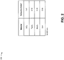
- Fig. 2 is an example table 200 of refractive indices for a set of materials that may be used for implementations, described herein. As shown in Fig. 2 , table 200 identifies a set of materials and a corresponding set of refractive indices for the set of materials. In this case, the set of refractive indices are determined for the set of materials with regard to light at approximately 900 nm wavelength. Other materials are possible and may differ from the materials depicted in table 200.
- hydrogenated silicon is associated with a relatively high refractive index of 3.65 relative to the refractive indices of niobium pentoxide (Nb 2 O 5 ) and/or tantalum pentoxide (Ta 2 O 5 ) of, respectively, 2.28 and 2.12.
- a ratio of the high refractive index material to the low refractive index material of a set of layers corresponds to a quantity of layers used to cause polarization beamsplitting for an optical filter.
- hydrogenated silicon being associated with a relatively high refractive index
- use of hydrogenated silicon as a high refractive index material with silicon dioxide as a low refractive index material with a refractive index of 1.47 results in a relatively high ratio of refractive indices relative to using another material, such as tantalum pentoxide or niobium pentoxide, as a high refractive index material.
- an optical filter using alternating layers of hydrogenated silicon and silicon dioxide can perform polarization beamsplitting with a reduced quantity of layers relative to using tantalum pentoxide or niobium pentoxide as a high index material, thereby reducing a cost and/or a size of the optical filter and improving a durability of the optical filter and/or a set of optical characteristics of the optical filter.
- Fig. 2 is provided merely as an example. Other examples are possible and may differ from what was described with regard to Fig. 2 .
- Fig. 3 is a diagram of example optical characteristics relating to using an example implementation described herein.
- a set of optical filters may be utilized for NIR polarization beam splitting.
- Chart 310 shows example optical characteristics of NIR polarization beamsplitting at an angle of incidence (AOI) of 45 degrees with a first optical filter using niobium pentoxide as a high index material and silicon dioxide as a low index material.
- the first optical filter is associated with a thickness of 15.5 micrometers ( ⁇ m) and 96 layers.
- Chart 320 shows example results of NIR polarization beamsplitting at an AOI of 45 degrees with a second optical filter using hydrogenated silicon as a high index material and silicon dioxide as a low index material.
- the second optical filter is associated with a thickness of 5.3 ⁇ m and 40 layers.
- an optical filter using hydrogenated silicon as a high index material performs NIR polarization beamsplitting with a reduced thickness and a reduced quantity of layers relative to using other materials as a high index material (e.g., niobium pentoxide), thereby reducing a cost and a size of the optical filter and improving durability of the optical filter.
- a high index material e.g., niobium pentoxide
- reference numbers 330 show a reflection percentage in the s-plane for the first optical filter and the second optical filter.
- the s-plane may refer to a first polarization of a p-plane polarization and an s-plane polarization orthogonal coordinate system.
- the second optical filter provides greater than or equal to 99% reflectance for s-plane visible light, thereby obviating a need for additional blocking filters as is required for the first optical filter to be utilized.
- reference numbers 340 show a transmission percentage in the p-plane for the first optical filter and the second optical filter.
- the second optical filter provides greater than or equal to 99% transmission for p-plane light at a range of approximately 890 nm to approximately 940 nm (e.g., NIR light), greater than or equal to 95% transmission for p-plane light at a range of approximately 890 nm to approximately 960 nm, approximately 890 nm to approximately 940 nm, approximately 940 nm to approximately 960 nm, or the like.
- an optical filter using hydrogenated silicon exhibits improved optical performance for NIR polarization beamsplitting with regard to out-of-band blocking and in-band transmissivity relative to another filter using another material with a lower refractive index as a high index material, such as niobium pentoxide.
- Fig. 3 shows an example relating to a particular value for transmission and reflectance over a particular spectral range and AOI
- examples described herein may exhibit similarly improved performance for other values of transmission and reflectance, over other spectral ranges and for other AOIs.
- Fig. 3 is provided merely as an example. Other examples are possible and may differ from what was described with regard to Fig. 3 .
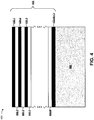
- Fig. 4 is a diagram of an example optical filter 400.
- Fig. 4 shows an example stackup of an optical filter using hydrogenated silicon as a high index material.
- optical filter 400 includes an optical filter coating portion 410 and a substrate 420.
- Optical filter coating portion 410 includes a set of optical filter layers.
- optical filter coating portion 410 includes a first set of layers 430-1 through 430 -N ( N ⁇ 1) and a second set of layers 440-1 through 440-( N +1).
- Layers 430 may include a set of layers of a high refractive index material (H layers), such as hydrogenated silicon layers.
- Layers 440 may include a set of layers of a low refractive index material (L layers), such as silicon dioxide layers, aluminum oxide (Al 2 O 3 ) layers, magnesium fluoride (MgF 2 ) layers, or the like.
- layers 430 and 440 may be stacked in a particular order, such as an (H-L) m ( m ⁇ 1) order, an (H-L) m -H order, an (L-H) m order, an L-(H-L) m order, or the like.
- layers 430 and 440 are positioned in an (H-L) n -H order with an H layer disposed at a surface of optical filter 400 and an H layer disposed at a surface of substrate 420.
- optical filter coating portion 410 may be associated with a particular quantity of layers, m.
- a hydrogenated silicon based optical filter may include 40 layers of alternating H layers and L layers.
- optical filter 400 may be associated with another quantity of layers, such as a range of 10 layers to 100 layers.
- each layer of optical filter coating portion 410 may be associated with a particular thickness.
- layers 430 and 440 may each be associated with a thickness of between 3 nm and 300 nm, resulting in optical filter coating portion 410 being associated with a thickness of between 1 ⁇ m and 100 ⁇ m.
- layers 430 and 440 may be associated with multiple thicknesses, such as a first thickness for layers 430 and a second thickness for layers 440, a first thickness for a first subset of layers 430 and a second thickness for a second subset of layers 430, a first thickness for a first subset of layers 440 and a second thickness for a second subset of layers 440, or the like.
- a layer thickness and/or a quantity of layers may be selected based on an intended set of optical characteristics, such as an intended passband, an intended reflectance, or the like.
- the layer thickness and/or the quantity of layers may be selected to permit a polarizing beamsplitter to be utilized for a spectral range of approximately 700 nm to approximately 1700 nm with a separation bandwidth of at least 10 nm.
- a particular hydrogenated silicon based material may be selected for the H layers 430.
- layers 430 and/or 440 may be associated with a particular extinction coefficient, such as an extinction coefficient of less than approximately 0.001, less than approximately 0.0007, less than approximately 0.0006, less than approximately 0.0005, an extinction coefficient of less than approximately 0.0003, an extinction coefficient of less than approximately 0.0001, or the like over a particular spectral range (e.g., the spectral range of approximately 800 nm to approximately 1100 nm, the spectral range of approximately 900 nm to approximately 1000 nm, the wavelength of approximately 954 nm, or the like).
- layers 430 may be selected and/or manufactured to include a refractive index of greater than approximately 3, approximately 3.5, approximately 3.6, approximately 3.7, approximately 3.75 or the like over a particular spectral range (e.g., the spectral range of approximately 800 nm to approximately 1100 nm, the spectral range of approximately 900 nm to approximately 1000 nm, the wavelength of approximately 954 nm, or the like.
- layers 430 may be selected to include a refractive index of approximately 3.6 at a wavelength of approximately 830 nm.
- layers 430 and/or 440 may be manufactured to cause a first portion of light to be blocked (e.g., less than approximately 800 nm, less than approximately 700 nm, etc.) and a second portion of light to be passed (e.g., a spectral range less than approximately 1700 nm, at approximately 1550 nm, less than approximately 1100 nm, etc.).
- a first portion of light e.g., less than approximately 800 nm, less than approximately 700 nm, etc.
- a second portion of light to be passed e.g., a spectral range less than approximately 1700 nm, at approximately 1550 nm, less than approximately 1100 nm, etc.
- a particular material may be selected for L layers 440.
- layers 440 may include a set of silicon dioxide (SiO 2 ) layers, a set of aluminum oxide (Al 2 O 3 ) layers, a set of titanium dioxide (TiO 2 ) layers, a set of niobium pentoxide (Nb 2 O 5 ) layers, a set of tantalum pentoxide (Ta 2 O 5 ) layers, a set of magnesium fluoride (MgF 2 ) layers, or the like.
- SiO 2 silicon dioxide
- Al 2 O 3 aluminum oxide
- TiO 2 titanium dioxide
- Nb 2 O 5 niobium pentoxide
- Ta 2 O 5 tantalum pentoxide
- MgF 2 magnesium fluoride
- layers 440 may be selected to include a refractive index lower than that of the layers 430 over, for example, a particular spectral range (e.g., the spectral range of approximately 800 nm to approximately 1100 nm, the spectral range of approximately 900 nm to approximately 1000 nm, the wavelength of approximately 954 nm, or the like).
- a particular spectral range e.g., the spectral range of approximately 800 nm to approximately 1100 nm, the spectral range of approximately 900 nm to approximately 1000 nm, the wavelength of approximately 954 nm, or the like.
- layers 440 may be selected to be associated with a refractive index of less than 3 over a particular spectral range (e.g., the spectral range of approximately 800 nm to approximately 1100 nm, the spectral range of approximately 900 nm to approximately 1000 nm, a spectral range of approximately 800 nm, the wavelength of approximately 954 nm, or the like).
- a particular spectral range e.g., the spectral range of approximately 800 nm to approximately 1100 nm, the spectral range of approximately 900 nm to approximately 1000 nm, a spectral range of approximately 800 nm, the wavelength of approximately 954 nm, or the like.
- layers 440 may be selected to be associated with a refractive index of less than 2.5 over a particular spectral range (e.g., the spectral range of approximately 800 nm to approximately 1100 nm, the spectral range of approximately 900 nm to approximately 1000 nm, a spectral range of approximately 800 nm, the wavelength of approximately 954 nm, or the like).
- a particular spectral range e.g., the spectral range of approximately 800 nm to approximately 1100 nm, the spectral range of approximately 900 nm to approximately 1000 nm, a spectral range of approximately 800 nm, the wavelength of approximately 954 nm, or the like.
- layers 440 may be selected to be associated with a refractive index of less than 2 over a particular spectral range (e.g., the spectral range of approximately 800 nm to approximately 1100 nm, the spectral range of approximately 900 nm to approximately 1000 nm, a spectral range of approximately 800 nm, the wavelength of approximately 954 nm, or the like).
- a particular spectral range e.g., the spectral range of approximately 800 nm to approximately 1100 nm, the spectral range of approximately 900 nm to approximately 1000 nm, a spectral range of approximately 800 nm, the wavelength of approximately 954 nm, or the like.
- layers 440 may be selected to be associated with a refractive index of less than 1.5 over a particular spectral range (e.g., the spectral range of approximately 800 nm to approximately 1100 nm, the spectral range of approximately 900 nm to approximately 1000 nm, the wavelength of approximately 954 nm, or the like).
- the particular material may be selected for L layers 440 based on a desired width of an out-of-band blocking spectral range, a desired center-wavelength shift associated with a change of AOI, or the like.
- optical filter coating portion 410 may be fabricated using a sputtering procedure.
- optical filter coating portion 410 may be fabricated using a pulsed-magnetron based sputtering procedure to sputter alternating layers 430 and 440 on a glass substrate.
- optical filter coating portion 410 may be associated with a relatively low center-wavelength shift with change in AOI.
- optical filter coating portion 410 may cause a center-wavelength shift of less than approximately 20 nm, approximately 15 nm, approximately 12 nm, or the like in magnitude with a change in incidence angle from 0° to 30°.
- optical filter coating portion 410 is attached to a substrate, such as substrate 420.
- optical filter coating portion 410 may be attached to a glass substrate.
- optical filter coating portion 410 may be associated with an incident medium, such as an air medium or glass medium, with a reflection of greater than 50% in a first polarization plane, with a transmission of greater than 50% in a second polarization plane, with a nominal AOI of incident light relative to a surface of optical filter 400 from 15° to 75°, and with a range of angles of incident light relative to the nominal AOI of 0° to 45°.
- optical filter 400 may be disposed between a set of prisms.
- an annealing procedure may be utilized to fabricate optical filter coating portion 410. For example, after sputter deposition of layers 430 and 440 on a substrate, optical filter 400 may be annealed to improve one or more optical characteristics of optical filter 400, such as reducing an absorption coefficient of optical filter 400 relative to another optical filter for which an annealing procedure is not performed.
- Fig. 4 is provided merely as an example. Other examples are possible and may differ from what was described with regard to Fig. 4 .
- a set of hydrogenated silicon layers may be used as a high index material for an optical filter coating of an optical filter to provide out-of-band blocking of visible light, transmission of NIR light, and polarization beamsplitting with a reduced thickness, cost, and time of manufacture relative to another type of material used for a set of high index layers.
- out-of-band blocking and in-band transmission are improved relative to another type of material.
- satisfying a threshold may refer to a value being greater than the threshold, more than the threshold, higher than the threshold, greater than or equal to the threshold, less than the threshold, fewer than the threshold, lower than the threshold, less than or equal to the threshold, equal to the threshold, etc.
Landscapes
- Physics & Mathematics (AREA)
- General Physics & Mathematics (AREA)
- Optics & Photonics (AREA)
- Electromagnetism (AREA)
- Engineering & Computer Science (AREA)
- Computer Networks & Wireless Communication (AREA)
- Signal Processing (AREA)
- Polarising Elements (AREA)
- Optical Filters (AREA)
- Optical Head (AREA)
- Switches Operated By Changes In Physical Conditions (AREA)
- Microscoopes, Condenser (AREA)
Abstract
Description
- In some instances, it may be desirable to block certain wavelengths of energy and/or only transmit certain wavelengths energy to a detector. For example, some detectors may be sensitive to energy in certain wavelengths. In one example, an optical transmitter may emit light that is ultimately received by an optical receiver. For example, in a gesture recognition system, the optical transmitter may transmit near infrared (NIR) light toward a user, and the NIR light may be reflected off the user toward the optical receiver. In this case, the optical receiver may capture information regarding the NIR light, and the information may be used to identify a gesture being performed by the user. For example, a device may use the information to generate a three dimensional representation of the user, and to identify the gesture being performed by the user based on the three dimensional representation. However, during transmission of the NIR light toward the user and/or during reflection from the user toward the optical receiver, ambient light may interfere with the NIR light. Thus, the optical receiver may be optically coupled to an optical filter, such as a bandpass filter, to filter ambient light and to pass through NIR light toward the optical receiver.
- In some instances, the optical filter may include a polarizing beamsplitter. In general, a polarizing beamsplitter physically separates an incident beam of energy into two linearly polarized sub-beams ("P" and "S"). One "sub-beam" contains "P" polarized energy (e.g., the electric field is parallel or within the plane of incidence of the incident beam). The second "sub-beam" contains "S" polarized energy (e.g., the electric field is perpendicular to the plane of incidence of the incident beam).
- According to some possible implementations, a polarizing optical coating may include a set of layers. The set of layers may include a first subset of layers. The first subset of layers may include hydrogenated silicon (Si:H) with a first refractive index. The set of layers may include a second subset of layers. The second subset of layers may include a material with a second refractive index. The second refractive index may be less than the first refractive index.
- According to some possible implementations, an optical filter may include a substrate. The optical filter may include a set of alternating high refractive index layers and low refractive index layers disposed onto the substrate to polarization beam split incident light. The set of alternating high refractive index layers and low refractive index may layers may be disposed such that a first polarization of the incident light with a spectral range of less than approximately 800 nanometers (nm) is reflected by the optical filter and a second polarization of the incident light with a spectral range of greater than approximately 800 nm is passed through by the optical filter. The high refractive index layers may be hydrogenated silicon (Si:H). The low refractive index layers may be silicon dioxide (SiO2).
- According to some possible implementations, an optical system may include an optical transmitter to emit near-infrared (NIR) light. The optical system may include a polarizing optical filter to filter an input optical signal and provide the filtered input optical signal. The input optical signal may include the NIR light from the optical transmitter and ambient light from another optical source. The polarizing optical filter may include a set of dielectric thin film layers. The set of dielectric thin film layers may include a first subset of layers of hydrogenated silicon with a first refractive index. The set of dielectric thin film layers may include second subset of layers of a material with a second refractive index less than the first refractive index. The filtered input optical signal may include a reduced intensity of ambient light relative to the input optical signal. An optical receiver may receive the filtered input optical signal and provide an output electrical signal.
- Thus, according to one aspect of the present invention, there is provided a polarizing optical coating, comprising a set of layers including:
- a first subset of layers, the first subset of layers comprising hydrogenated silicon (Si:H) with a first refractive index; and
- a second subset of layers, the second subset of layers comprising a material with a second refractive index, and the second refractive index being less than the first refractive index.
- Optionally, the material includes at least one of:
- a silicon dioxide (SiO2) material,
- an aluminum oxide (Al2O3) material,
- a titanium dioxide (TiO2) material,
- a niobium pentoxide (Nb2O5) material,
- a tantalum pentoxide (Ta2O5) material, or
- a magnesium fluoride (MgF2) material.
- Optionally, the first subset of layers are high refractive index layers (H) and the second subset of layers are low refractive index layers (L); and
- where the set of layers are arranged in at least one of:
- an (H-L) m order,
- an (H-L) m -H order,
- an (L-H)m order, or
- an L-(H-L) m order,
- where m is a quantity of alternating H and L layers.
- Optionally, the set of layers is to block a threshold portion of light associated with a spectral range of less than approximately 700 nanometers (nm).
- Optionally, the set of layers is to pass a threshold portion of light associated with a spectral range of less than approximately 1700 nanometers (nm).
- Optionally, the first refractive index is greater than approximately 3 at a wavelength of approximately 900 nanometers (nm).
- Optionally, the first refractive index is approximately 3.6 at a wavelength of approximately 830 nanometers (nm).
- Optionally, the first subset of layers is associated with an extinction coefficient of less than approximately 0.0006 at a particular spectral range.
- Optionally, the second refractive index is less than 3 at a spectral range of approximately 800 nanometers (nm) to approximately 1100 nm.
- Optionally, the second refractive index is less than 2 at a spectral range of approximately 800 nanometers (nm) to approximately 1100 nm.
- Optionally, the polarizing optical coating is a polarization beam splitter.
- Optionally, the polarizing optical coating covers a spectral range from 700 nanometers (nm) to 1700 with a separation bandwidth of at least 10 nm.
- Optionally, the polarizing optical coating is associated with greater than 50% reflection in a first plane of polarization and greater than 50% transmission in a second plane of polarization, with the first plane of polarization being orthogonal to the second plane of polarization.
- Optionally, a nominal angle of incidence of light relative to a surface of the polarizing optical coating is between 15 degrees and 75 degrees.
- Optionally, a range of angles of light relative to a nominal angle of incidence is between 0 degrees and 45 degrees.
- According to a second aspect of the present invention, there is provided an optical filter, comprising:
- a substrate; and
- a set of alternating high refractive index layers and low refractive index layers disposed onto the substrate to polarization beam split incident light,
- such that a first polarization of the incident light with a spectral range of less than approximately 800 nanometers (nm) is reflected by the optical filter and a second polarization of the incident light with a spectral range of greater than approximately 800 nm is passed through by the optical filter,
- the high refractive index layers being hydrogenated silicon (Si:H),
- the low refractive index layers being silicon dioxide (SiO2).
- Optionally, the second polarization of the incident light is in the p-plane and where the first polarization of the incident light is in the s-plane; and
where the optical filter is associated with greater than or equal to 99% transmission for the second polarization of the incident light at a spectral range of approximately 890 nm to approximately 940 nm; and
where the optical filter is associated with greater than or equal to 99% reflectance for the incident light in the s-plane. - Optionally, the second polarization of the incident light is in the p-plane and where the first polarization of the incident light is in the s-plane; and
where the optical filter is associated with greater than or equal to 95% transmission for the second polarization of the incident light at a spectral range of at least one of: - approximately 890 nm to approximately 940 nm, or
- approximately 930 nm to approximately 960; and
- where the optical filter is associated with greater than or equal to 95% reflectance for the incident light in the s-plane.
- According to a third aspect of the present invention, there is provided an optical system, comprising:
- an optical transmitter to emit near-infrared (NIR) light;
- a polarizing optical filter to filter an input optical signal and provide the filtered input optical signal, the input optical signal including the NIR light from the optical transmitter and ambient light from another optical source, ad the polarizing optical filter including a set of dielectric thin film layers, the set of dielectric thin film layers including a first subset of layers of hydrogenated silicon with a first refractive index, and a second subset of layers of a material with a second refractive index less than the first refractive index,
- the filtered input optical signal including a reduced intensity of ambient light relative to the input optical signal; and
- an optical receiver to receive the filtered input optical signal and provide an output electrical signal.
- Optionally, the polarizing optical filter is to polarization beam split the input optical signal to provide the filtered input optical signal.
-
-
Fig. 1 is a diagram of an overview of an example implementation described herein; -
Fig. 2 is a table of refractive indices for a set of materials relating to an example implementation described herein; -
Fig. 3 is a diagram of example optical characteristics relating to using an example implementation described herein; and -
Fig. 4 is a diagram of an example implementation described herein. - The following detailed description of example implementations refers to the accompanying drawings. The same reference numbers in different drawings may identify the same or similar elements. As used herein, the terms "substantially," "approximately," and "about" indicate a range of values within +/- 5% of a stated value.
- An optical receiver may receive light initiating from an optical source, such as an optical transmitter. For example, the optical receiver may receive near infrared (NIR) light from the optical transmitter and reflected off a target, such as a user or an object. In this case, the optical receiver may receive the NIR light as well as ambient light, such as visible spectrum light. The ambient light may reduce an accuracy of a determination relating to the NIR light. For example, in a gesture recognition system, the ambient light may reduce an accuracy of generation of a three-dimensional image of the target based on the NIR light. Thus, the optical receiver may be optically coupled to an optical filter, such as a bandpass filter, to filter ambient light and to pass through NIR light toward the optical receiver.
- The optical filter may include a set of dielectric thin film layers. The set of dielectric thin film layers are selected and deposited to block a portion of out-of-band light below and/or above a particular threshold, such as below 700 nanometers (nm). For example, the set of dielectric thin film layers may be selected to filter out the ambient light. The optical filter may perform a polarization beamsplitting functionality for the light. For example, the optical filter may reflect a first portion of the light with a first polarization and may pass through a second portion of the light with a second polarization when the second polarization is desired to be received by the optical receiver.
- However, an excess quantity of dielectric thin film layers may result in a relatively thick coating. The relatively thick coating may be expensive to manufacture as a result of sequential deposition of each dielectric thin film layer, and may experience an excessive stress condition resulting in poor durability. Moreover, the relatively thick coating may be associated with an insufficient flatness for a polarization beamsplitting functionality. Furthermore, when silicon layers are used for a portion of the dielectric thin film layers, the silicon layers may be associated with a relatively high absorption coefficient for light below approximately 1100 nm, which may make the silicon layers unsuitable for utilization as a high index material in a polarizing beamsplitter with a relatively high transmission requirement for a pass band below approximately 1100 nm.
- Implementations, described, herein, may utilize a hydrogenated silicon (Si:H) material as a set of high index layers for polarizing optical coating, such as an optical polarizing filter. In this way, the optical filter (i.e., the polarizing optical coating) may reflect ambient light and pass through NIR light, and may perform a polarization beamsplitting functionality. Based on using hydrogenated silicon as a material for the set of high index layers of the optical filter, a thickness of the optical filter and a cost of the optical filter are reduced, and a durability of the optical filter and a set of optical characteristics of the optical filter are improved relative to utilizing another type of material for the optical filter.
- In one general aspect of the present invention, there is provide a
Fig. 1 is a diagram of an overview of anexample implementation 100 described herein. As shown inFig. 1 ,example implementation 100 includes asensor system 110.Sensor system 110 may be a portion of an optical system, and may provide an electrical output corresponding to a sensor determination.Sensor system 110 includes anoptical filter structure 120, which includes anoptical filter 130, and anoptical sensor 140. For example,optical filter structure 120 may include a polarizing beamsplitteroptical filter 130 that performs a passband filtering functionality. - It should be understood that the implementations, described herein may be utilized for a traditional polarizing beamsplitter (e.g., the P-polarized energy is transmitted and S-polarized energy is reflected) and/or a reverse polarization beamsplitting (e.g., the P-polarized energy is reflected and S-polarized energy is transmitted).
- Although implementations, described herein, may be described in terms of an optical filter in a sensor system, implementations described herein may be used in another type of system, may be used external to a system, or the like.
- As further shown in
Fig. 1 , and byreference number 150, an input optical signal is directed towardoptical filter structure 120 that is a polarizing optical coating. The input optical signal may include but is not limited to NIR light initially emitted by an optical transmitter and ambient light from the environment in whichsensor system 110 is being utilized. For example, an optical transmitter may direct NIR light toward a user for a gesture recognition system, and the NIR light may be reflected off the user towardoptical sensor 140 to permitoptical sensor 140 to perform a measurement of the NIR light. In this case, ambient light may be directed towardoptical sensor 140 from one or more ambient light sources (e.g., a light bulb or the sun). In another example, the optical transmitter may direct NIR light toward another type of object, such as a for detecting objects in proximity to a vehicle, detecting objects in proximity to a blind person, detecting a proximity to an object (e.g., using a LIDAR technique), or the like, andoptical sensor 140 may receive the NIR light and ambient light as a result. - As further shown in
Fig. 1 , and byreference number 160, a first portion of the optical signal is reflected byoptical filter 130 andoptical filter structure 120 with a first polarization. For example, alternating hydrogenated silicon layers (e.g., a high index material) and another type of material layers (e.g., a low index material, such as silicon dioxide (SiO2)) ofoptical filter 130, may cause the first polarization of light to be reflected in a first direction. (It should be noted that any layer may additionally include nitrogen, germanium, argon, and/or other elements.) As shown byreference number 170, a second portion of the optical signal is passed through byoptical filter 130 andoptical filter structure 120 with a second polarization. For example,optical filter 130 may pass through a second polarization of light in a second direction towardoptical sensor 140. In this case,optical filter 130 blocks visible light without excessively blocking NIR light, as described in more detail herein. - As further shown in
Fig. 1 , and byreference number 180, based on the second portion of the optical signal being passed tooptical sensor 140,optical sensor 140 may provide an output electrical signal forsensor system 110, such as for use in recognizing a gesture of the user or detecting the presence of an object. In some implementations, another arrangement ofoptical filter 130 andoptical sensor 140 may be utilized. For example, rather than passing the second portion of the optical signal collinearly with the input optical signal,optical filter 130 may direct the second portion of the optical signal in another direction toward a differently locatedoptical sensor 140. - In a traditional polarizing beamsplitter, the first polarization portion of input
optical signal 160 may be reflected S-polarized light and the second polarization portion of inputoptical signal 170 may be transmitted P-polarized light. In contrast, in a reverse polarizing beamsplitter, the first polarization portion of inputoptical signal 160 may be reflected P-polarized light and the second polarization portion of inputoptical signal 170 may be transmitted S-polarized light. It should also be understood that in some implementations, the energy may travel in the opposite direction to that shown in inFIG. 1 , and instead of polarizing one beam, theoptical filter 130 may combine two beams. - As indicated above,
Fig. 1 is provided merely as an example. Other examples are possible and may differ from what was described with regard toFig. 1 . -
Fig. 2 is an example table 200 of refractive indices for a set of materials that may be used for implementations, described herein. As shown inFig. 2 , table 200 identifies a set of materials and a corresponding set of refractive indices for the set of materials. In this case, the set of refractive indices are determined for the set of materials with regard to light at approximately 900 nm wavelength. Other materials are possible and may differ from the materials depicted in table 200. - As shown in
Fig. 2 , hydrogenated silicon (Si:H) is associated with a relatively high refractive index of 3.65 relative to the refractive indices of niobium pentoxide (Nb2O5) and/or tantalum pentoxide (Ta2O5) of, respectively, 2.28 and 2.12. A ratio of the high refractive index material to the low refractive index material of a set of layers corresponds to a quantity of layers used to cause polarization beamsplitting for an optical filter. For example, based on hydrogenated silicon being associated with a relatively high refractive index, use of hydrogenated silicon as a high refractive index material with silicon dioxide as a low refractive index material with a refractive index of 1.47, results in a relatively high ratio of refractive indices relative to using another material, such as tantalum pentoxide or niobium pentoxide, as a high refractive index material. In this case, an optical filter using alternating layers of hydrogenated silicon and silicon dioxide can perform polarization beamsplitting with a reduced quantity of layers relative to using tantalum pentoxide or niobium pentoxide as a high index material, thereby reducing a cost and/or a size of the optical filter and improving a durability of the optical filter and/or a set of optical characteristics of the optical filter. - As indicated above,
Fig. 2 is provided merely as an example. Other examples are possible and may differ from what was described with regard toFig. 2 . -
Fig. 3 is a diagram of example optical characteristics relating to using an example implementation described herein. - As shown in
Fig. 3 , and bycharts - As further shown in
Fig. 3 , reference numbers 330 show a reflection percentage in the s-plane for the first optical filter and the second optical filter. The s-plane may refer to a first polarization of a p-plane polarization and an s-plane polarization orthogonal coordinate system. In this case, the second optical filter provides greater than or equal to 99% reflectance for s-plane visible light, thereby obviating a need for additional blocking filters as is required for the first optical filter to be utilized. As further shown inFig. 3 , reference numbers 340 show a transmission percentage in the p-plane for the first optical filter and the second optical filter. In this case, the second optical filter provides greater than or equal to 99% transmission for p-plane light at a range of approximately 890 nm to approximately 940 nm (e.g., NIR light), greater than or equal to 95% transmission for p-plane light at a range of approximately 890 nm to approximately 960 nm, approximately 890 nm to approximately 940 nm, approximately 940 nm to approximately 960 nm, or the like. In this way, an optical filter using hydrogenated silicon exhibits improved optical performance for NIR polarization beamsplitting with regard to out-of-band blocking and in-band transmissivity relative to another filter using another material with a lower refractive index as a high index material, such as niobium pentoxide. - Although
Fig. 3 shows an example relating to a particular value for transmission and reflectance over a particular spectral range and AOI, examples described herein may exhibit similarly improved performance for other values of transmission and reflectance, over other spectral ranges and for other AOIs. - As indicated above,
Fig. 3 is provided merely as an example. Other examples are possible and may differ from what was described with regard toFig. 3 . -
Fig. 4 is a diagram of an exampleoptical filter 400.Fig. 4 shows an example stackup of an optical filter using hydrogenated silicon as a high index material. As further shown inFig. 4 ,optical filter 400 includes an opticalfilter coating portion 410 and asubstrate 420. - Optical
filter coating portion 410 includes a set of optical filter layers. For example, opticalfilter coating portion 410 includes a first set of layers 430-1 through 430-N(N≥ 1) and a second set of layers 440-1 through 440-(N+1).Layers 430 may include a set of layers of a high refractive index material (H layers), such as hydrogenated silicon layers.Layers 440 may include a set of layers of a low refractive index material (L layers), such as silicon dioxide layers, aluminum oxide (Al2O3) layers, magnesium fluoride (MgF2) layers, or the like. In some implementations, layers 430 and 440 may be stacked in a particular order, such as an (H-L) m (m ≥ 1) order, an (H-L) m -H order, an (L-H)m order, an L-(H-L) m order, or the like. For example, as shown, layers 430 and 440 are positioned in an (H-L) n -H order with an H layer disposed at a surface ofoptical filter 400 and an H layer disposed at a surface ofsubstrate 420. - In some implementations, optical
filter coating portion 410 may be associated with a particular quantity of layers, m. For example, as described with regard toFig. 3 , a hydrogenated silicon based optical filter may include 40 layers of alternating H layers and L layers. In another example,optical filter 400 may be associated with another quantity of layers, such as a range of 10 layers to 100 layers. In some implementations, each layer of opticalfilter coating portion 410 may be associated with a particular thickness. For example, layers 430 and 440 may each be associated with a thickness of between 3 nm and 300 nm, resulting in opticalfilter coating portion 410 being associated with a thickness of between 1 µm and 100 µm. In some implementations, layers 430 and 440 may be associated with multiple thicknesses, such as a first thickness forlayers 430 and a second thickness forlayers 440, a first thickness for a first subset oflayers 430 and a second thickness for a second subset oflayers 430, a first thickness for a first subset oflayers 440 and a second thickness for a second subset oflayers 440, or the like. In this case, a layer thickness and/or a quantity of layers may be selected based on an intended set of optical characteristics, such as an intended passband, an intended reflectance, or the like. For example, the layer thickness and/or the quantity of layers may be selected to permit a polarizing beamsplitter to be utilized for a spectral range of approximately 700 nm to approximately 1700 nm with a separation bandwidth of at least 10 nm. - In some implementations, a particular hydrogenated silicon based material may be selected for the H layers 430. In some implementations, layers 430 and/or 440 may be associated with a particular extinction coefficient, such as an extinction coefficient of less than approximately 0.001, less than approximately 0.0007, less than approximately 0.0006, less than approximately 0.0005, an extinction coefficient of less than approximately 0.0003, an extinction coefficient of less than approximately 0.0001, or the like over a particular spectral range (e.g., the spectral range of approximately 800 nm to approximately 1100 nm, the spectral range of approximately 900 nm to approximately 1000 nm, the wavelength of approximately 954 nm, or the like). In some implementations, layers 430 may be selected and/or manufactured to include a refractive index of greater than approximately 3, approximately 3.5, approximately 3.6, approximately 3.7, approximately 3.75 or the like over a particular spectral range (e.g., the spectral range of approximately 800 nm to approximately 1100 nm, the spectral range of approximately 900 nm to approximately 1000 nm, the wavelength of approximately 954 nm, or the like. In another example, layers 430 may be selected to include a refractive index of approximately 3.6 at a wavelength of approximately 830 nm. In some implementations, layers 430 and/or 440 may be manufactured to cause a first portion of light to be blocked (e.g., less than approximately 800 nm, less than approximately 700 nm, etc.) and a second portion of light to be passed (e.g., a spectral range less than approximately 1700 nm, at approximately 1550 nm, less than approximately 1100 nm, etc.).
- In some implementations, a particular material may be selected for L layers 440. For example, layers 440 may include a set of silicon dioxide (SiO2) layers, a set of aluminum oxide (Al2O3) layers, a set of titanium dioxide (TiO2) layers, a set of niobium pentoxide (Nb2O5) layers, a set of tantalum pentoxide (Ta2O5) layers, a set of magnesium fluoride (MgF2) layers, or the like. In this case, layers 440 may be selected to include a refractive index lower than that of the
layers 430 over, for example, a particular spectral range (e.g., the spectral range of approximately 800 nm to approximately 1100 nm, the spectral range of approximately 900 nm to approximately 1000 nm, the wavelength of approximately 954 nm, or the like). For example, layers 440 may be selected to be associated with a refractive index of less than 3 over a particular spectral range (e.g., the spectral range of approximately 800 nm to approximately 1100 nm, the spectral range of approximately 900 nm to approximately 1000 nm, a spectral range of approximately 800 nm, the wavelength of approximately 954 nm, or the like). - In another example, layers 440 may be selected to be associated with a refractive index of less than 2.5 over a particular spectral range (e.g., the spectral range of approximately 800 nm to approximately 1100 nm, the spectral range of approximately 900 nm to approximately 1000 nm, a spectral range of approximately 800 nm, the wavelength of approximately 954 nm, or the like). In another example, layers 440 may be selected to be associated with a refractive index of less than 2 over a particular spectral range (e.g., the spectral range of approximately 800 nm to approximately 1100 nm, the spectral range of approximately 900 nm to approximately 1000 nm, a spectral range of approximately 800 nm, the wavelength of approximately 954 nm, or the like). In another example, layers 440 may be selected to be associated with a refractive index of less than 1.5 over a particular spectral range (e.g., the spectral range of approximately 800 nm to approximately 1100 nm, the spectral range of approximately 900 nm to approximately 1000 nm, the wavelength of approximately 954 nm, or the like). In some implementations, the particular material may be selected for L layers 440 based on a desired width of an out-of-band blocking spectral range, a desired center-wavelength shift associated with a change of AOI, or the like.
- In some implementations, optical
filter coating portion 410 may be fabricated using a sputtering procedure. For example, opticalfilter coating portion 410 may be fabricated using a pulsed-magnetron based sputtering procedure to sputter alternatinglayers filter coating portion 410 may be associated with a relatively low center-wavelength shift with change in AOI. For example, opticalfilter coating portion 410 may cause a center-wavelength shift of less than approximately 20 nm, approximately 15 nm, approximately 12 nm, or the like in magnitude with a change in incidence angle from 0° to 30°. In some implementations, opticalfilter coating portion 410 is attached to a substrate, such assubstrate 420. For example, opticalfilter coating portion 410 may be attached to a glass substrate. In some implementations, opticalfilter coating portion 410 may be associated with an incident medium, such as an air medium or glass medium, with a reflection of greater than 50% in a first polarization plane, with a transmission of greater than 50% in a second polarization plane, with a nominal AOI of incident light relative to a surface ofoptical filter 400 from 15° to 75°, and with a range of angles of incident light relative to the nominal AOI of 0° to 45°. In some implementations,optical filter 400 may be disposed between a set of prisms. - In some implementations, an annealing procedure may be utilized to fabricate optical
filter coating portion 410. For example, after sputter deposition oflayers optical filter 400 may be annealed to improve one or more optical characteristics ofoptical filter 400, such as reducing an absorption coefficient ofoptical filter 400 relative to another optical filter for which an annealing procedure is not performed. - As indicated above,
Fig. 4 is provided merely as an example. Other examples are possible and may differ from what was described with regard toFig. 4 . - In this way, a set of hydrogenated silicon layers may be used as a high index material for an optical filter coating of an optical filter to provide out-of-band blocking of visible light, transmission of NIR light, and polarization beamsplitting with a reduced thickness, cost, and time of manufacture relative to another type of material used for a set of high index layers. Moreover, based on using hydrogenated silicon, out-of-band blocking and in-band transmission are improved relative to another type of material.
- The foregoing disclosure provides illustration and description, but is not intended to be exhaustive or to limit the implementations to the precise form disclosed. Modifications and variations are possible in light of the above disclosure or may be acquired from practice of the implementations.
- Some implementations are described herein in connection with thresholds. As used herein, satisfying a threshold may refer to a value being greater than the threshold, more than the threshold, higher than the threshold, greater than or equal to the threshold, less than the threshold, fewer than the threshold, lower than the threshold, less than or equal to the threshold, equal to the threshold, etc.
- Even though particular combinations of features are recited in the claims and/or disclosed in the specification, these combinations are not intended to limit the disclosure of possible implementations. In fact, many of these features may be combined in ways not specifically recited in the claims and/or disclosed in the specification. Although each dependent claim listed below may directly depend on only one claim, the disclosure of possible implementations includes each dependent claim in combination with every other claim in the claim set.
- No element, act, or instruction used herein should be construed as critical or essential unless explicitly described as such. Also, as used herein, the articles "a" and "an" are intended to include one or more items, and may be used interchangeably with "one or more." Furthermore, as used herein, the term "set" is intended to include one or more items (e.g., related items, unrelated items, a combination of related items, and unrelated items, etc.), and may be used interchangeably with "one or more." Where only one item is intended, the term "one" or similar language is used. Also, as used herein, the terms "has," "have," "having," or the like are intended to be open-ended terms. Further, the phrase "based on" is intended to mean "based, at least in part, on" unless explicitly stated otherwise.
Claims (15)
- A polarizing optical coating, comprising a set of layers including:a first subset of layers, the first subset of layers comprising hydrogenated silicon (Si:H) with a first refractive index; anda second subset of layers, the second subset of layers comprising a material with a second refractive index, and the second refractive index being less than the first refractive index.
- The polarizing optical coating of claim 1, where the material includes at least one of:a silicon dioxide (SiO2) material,an aluminum oxide (Al2O3) material,a titanium dioxide (TiO2) material,a niobium pentoxide (Nb2O5) material,a tantalum pentoxide (Ta2O5) material, ora magnesium fluoride (MgF2) material.
- The polarizing optical coating of claim 1 or claim 2, where the first subset of layers are high refractive index layers (H) and the second subset of layers are low refractive index layers (L); and
where the set of layers are arranged in at least one of:an (H-L) m order,an (H-L) m -H order,an (L-H)m order, oran L-(H-L) m order,
where m is a quantity of alternating H and L layers. - The polarizing optical coating of any one of the preceding claims, where the set of layers is either:(i) to block a threshold portion of light associated with a spectral range of less than approximately 700 nanometers (nm); or(ii) to pass a threshold portion of light associated with a spectral range of less than approximately 1700 nanometers (nm); or(iii) both (i) and (ii).
- The polarizing optical coating of any one of the preceding claims, where the first refractive index is greater than approximately 3 at a wavelength of approximately 900 nanometers (nm), and optionally the first refractive index is approximately 3.6 at a wavelength of approximately 830 nanometers (nm).
- The polarizing optical coating of any one of the preceding claims, where the first subset of layers is associated with an extinction coefficient of less than approximately 0.0006 at a particular spectral range.
- The polarizing optical coating of any one of the preceding claims, where the second refractive index is less than 3, optionally less than 2, at a spectral range of approximately 800 nanometers (nm) to approximately 1100 nm.
- The polarizing optical coating of any one of the preceding claims, where the polarizing optical coating is a polarization beam splitter.
- The polarizing optical coating of any one of the preceding claims, where the polarizing optical coating covers a spectral range from 700 nanometers (nm) to 1700 with a separation bandwidth of at least 10 nm.
- The polarizing optical coating of any one of the preceding claims, where the polarizing optical coating is associated with greater than 50% reflection in a first plane of polarization and greater than 50% transmission in a second plane of polarization,
the first plane of polarization being orthogonal to the second plane of polarization. - The polarizing optical coating of any one of the preceding claims, where a nominal angle of incidence of light relative to a surface of the polarizing optical coating is between 15 degrees and 75 degrees.
- The polarizing optical coating of any one of the preceding claims, where a range of angles of light relative to a nominal angle of incidence is between 0 degrees and 45 degrees.
- An optical filter, comprising:a substrate; anda set of alternating high refractive index layers and low refractive index layers disposed onto the substrate to polarization beam split incident light,such that a first polarization of the incident light with a spectral range of less than approximately 800 nanometers (nm) is reflected by the optical filter and a second polarization of the incident light with a spectral range of greater than approximately 800 nm is passed through by the optical filter,the high refractive index layers being hydrogenated silicon (Si:H),the low refractive index layers being silicon dioxide (SiO2).
- The optical filter of claim 13 where the second polarization of the incident light is in the p-plane and where the first polarization of the incident light is in the s-plane; and
where the optical filter is associated with either(i) greater than or equal to 99% transmission for the second polarization of the incident light at a spectral range of approximately 890 nm to approximately 940 nm; or(ii) greater than or equal to 95% transmission for the second polarization of the incident light at a spectral range of at least one of:and where the optical filter is associated with greater than or equal to 95% reflectance for the incident light in the s-plane.approximately 890 nm to approximately 940 nm, orapproximately 930 nm to approximately 960; - An optical system, comprising:an optical transmitter to emit near-infrared (NIR) light;a polarizing optical filter to filter an input optical signal and provide the filtered input optical signal, the input optical signal including the NIR light from the optical transmitter and ambient light from another optical source, the polarizing optical filter including a set of dielectric thin film layers, the set of dielectric thin film layers including:a first subset of layers of hydrogenated silicon with a first refractive index, and a second subset of layers of a material with a second refractive index less than the first refractive index,the filtered input optical signal including a reduced intensity of ambient light relative to the input optical signal; and an optical receiver to receive the filtered input optical signal and provide an output electrical signal.
Applications Claiming Priority (1)
| Application Number | Priority Date | Filing Date | Title |
|---|---|---|---|
| US15/431,344 US10914961B2 (en) | 2017-02-13 | 2017-02-13 | Optical polarizing filter |
Publications (3)
| Publication Number | Publication Date |
|---|---|
| EP3361295A2 true EP3361295A2 (en) | 2018-08-15 |
| EP3361295A3 EP3361295A3 (en) | 2018-11-14 |
| EP3361295B1 EP3361295B1 (en) | 2023-03-15 |
Family
ID=61024626
Family Applications (1)
| Application Number | Title | Priority Date | Filing Date |
|---|---|---|---|
| EP18153121.1A Active EP3361295B1 (en) | 2017-02-13 | 2018-01-24 | Optical polarizing filter |
Country Status (8)
| Country | Link |
|---|---|
| US (1) | US10914961B2 (en) |
| EP (1) | EP3361295B1 (en) |
| JP (1) | JP6932656B2 (en) |
| KR (1) | KR102444466B1 (en) |
| CN (1) | CN108427154B (en) |
| AU (2) | AU2018200642A1 (en) |
| CA (1) | CA2993063C (en) |
| TW (1) | TWI735736B (en) |
Families Citing this family (17)
| Publication number | Priority date | Publication date | Assignee | Title |
|---|---|---|---|---|
| CN110579829A (en) * | 2018-07-26 | 2019-12-17 | 蓝思科技(长沙)有限公司 | Near-infrared filter, preparation method thereof and filtering equipment |
| CN109270616B (en) * | 2018-10-25 | 2021-02-26 | 杭州灯之塔科技有限公司 | Multi-valley transmission element and preparation method thereof |
| JP7251099B2 (en) * | 2018-10-31 | 2023-04-04 | 日本電気硝子株式会社 | Bandpass filter and manufacturing method thereof |
| US10962694B2 (en) | 2018-11-02 | 2021-03-30 | Viavi Solutions Inc. | Stepped structure optical filter |
| CN111290064A (en) * | 2018-11-22 | 2020-06-16 | 福州高意光学有限公司 | Polarization-independent optical filter |
| US11650361B2 (en) * | 2018-12-27 | 2023-05-16 | Viavi Solutions Inc. | Optical filter |
| CN112114394B (en) * | 2019-06-21 | 2023-03-31 | 福州高意光学有限公司 | Optical filter and sensor system with temperature compensation effect |
| JP7275946B2 (en) | 2019-07-10 | 2023-05-18 | セイコーエプソン株式会社 | Optical filters and electronics |
| KR102151947B1 (en) * | 2019-07-26 | 2020-09-04 | 송영진 | Optical filter and sensor system having the same, and halogenated amorphous silicon film manufacturing method for optical filter |
| CN110456440A (en) * | 2019-08-28 | 2019-11-15 | 山东劳动职业技术学院(山东劳动技师学院) | A kind of infrared polarizer of three layer line grid structure of metal-dielectric-metal |
| CN113126405B (en) * | 2019-12-31 | 2022-12-27 | 华为技术有限公司 | Projection device and projection interaction method |
| CN114089460A (en) * | 2020-08-24 | 2022-02-25 | 福州高意光学有限公司 | Low-angle offset optical filter |
| JP7484608B2 (en) * | 2020-09-17 | 2024-05-16 | セイコーエプソン株式会社 | Optical filters and electronic devices |
| CN112130339B (en) * | 2020-09-29 | 2022-08-12 | 苏州众为光电有限公司 | Laser polarization beam combination system |
| CN112130340B (en) * | 2020-09-29 | 2022-08-16 | 苏州众为光电有限公司 | Polarization beam splitter of ultra wide band |
| CN116802165A (en) | 2021-03-25 | 2023-09-22 | 肖特股份有限公司 | Near-infrared transparent, visible light absorbing coatings and coated glass substrates |
| KR20230150640A (en) | 2022-04-22 | 2023-10-31 | 현대자동차주식회사 | Infrared reflector for lidar |
Family Cites Families (22)
| Publication number | Priority date | Publication date | Assignee | Title |
|---|---|---|---|---|
| EP0573905A1 (en) | 1992-06-08 | 1993-12-15 | Minnesota Mining And Manufacturing Company | Retroreflecting polarizer for presentation systems |
| JPH06214115A (en) * | 1993-01-13 | 1994-08-05 | Sony Corp | Image pickup device |
| US5882774A (en) | 1993-12-21 | 1999-03-16 | Minnesota Mining And Manufacturing Company | Optical film |
| US5912762A (en) * | 1996-08-12 | 1999-06-15 | Li; Li | Thin film polarizing device |
| JPH1123842A (en) * | 1997-07-03 | 1999-01-29 | Minolta Co Ltd | Polarizing beam splitter, illumination optical system having the polarizing beam splitter, and projector |
| JP4028282B2 (en) | 2002-04-11 | 2007-12-26 | 日本電信電話株式会社 | Optical multilayer filter |
| JP4574439B2 (en) * | 2004-08-09 | 2010-11-04 | キヤノン株式会社 | Polarization separating element and projection apparatus having the same |
| WO2010025536A1 (en) | 2008-09-08 | 2010-03-11 | National Research Council Of Canada | Thin film optical filters with an integral air layer |
| EP2507599B1 (en) | 2009-11-30 | 2025-06-11 | IMEC vzw | Integrated circuit for spectral imaging system |
| JP5620576B2 (en) | 2010-07-15 | 2014-11-05 | フラウンホッファー−ゲゼルシャフト ツァ フェルダールング デァ アンゲヴァンテン フォアシュンク エー.ファオ | Optical bandpass filter system, especially for multichannel frequency selective measurement |
| IN2014CN02966A (en) | 2011-11-04 | 2015-07-03 | Imec | |
| EP2773929B1 (en) | 2011-11-04 | 2023-12-13 | IMEC vzw | Spectral camera with mosaic of filters for each image pixel |
| IN2014CN03038A (en) | 2011-11-04 | 2015-07-03 | Imec | |
| TWI684031B (en) * | 2012-07-16 | 2020-02-01 | 美商唯亞威方案公司 | Optical filter and sensor system |
| US9212996B2 (en) | 2013-08-05 | 2015-12-15 | Tellspec, Inc. | Analyzing and correlating spectra, identifying samples and their ingredients, and displaying related personalized information |
| US9645075B2 (en) | 2013-11-26 | 2017-05-09 | nanoLambda Korea | Multispectral imager with hybrid double layer filter array |
| EP3839585B1 (en) | 2015-02-18 | 2022-11-09 | Materion Corporation | Near infrared optical interference filters with improved transmission |
| CN105388625B (en) * | 2015-12-23 | 2018-11-13 | 浙江大学 | A kind of wearing display beam splitter and preparation method thereof |
| US10168459B2 (en) * | 2016-11-30 | 2019-01-01 | Viavi Solutions Inc. | Silicon-germanium based optical filter |
| US11215741B2 (en) * | 2018-01-17 | 2022-01-04 | Viavi Solutions Inc. | Angle of incidence restriction for optical filters |
| US11009636B2 (en) * | 2018-03-13 | 2021-05-18 | Viavi Solutions Inc. | Sensor window to provide different opacity and transmissivity at different spectral ranges |
| US10948640B2 (en) * | 2018-03-13 | 2021-03-16 | Viavi Solutions Inc. | Sensor window with a set of layers configured to a particular color and associated with a threshold opacity in a visible spectral range wherein the color is a color-matched to a surface adjacent to the sensor window |
-
2017
- 2017-02-13 US US15/431,344 patent/US10914961B2/en active Active
-
2018
- 2018-01-24 JP JP2018009735A patent/JP6932656B2/en active Active
- 2018-01-24 EP EP18153121.1A patent/EP3361295B1/en active Active
- 2018-01-25 TW TW107102717A patent/TWI735736B/en active
- 2018-01-25 AU AU2018200642A patent/AU2018200642A1/en not_active Abandoned
- 2018-01-26 CA CA2993063A patent/CA2993063C/en active Active
- 2018-02-08 KR KR1020180015916A patent/KR102444466B1/en active Active
- 2018-02-13 CN CN201810149226.6A patent/CN108427154B/en active Active
-
2023
- 2023-02-08 AU AU2023200691A patent/AU2023200691B2/en active Active
Non-Patent Citations (1)
| Title |
|---|
| None |
Also Published As
| Publication number | Publication date |
|---|---|
| US10914961B2 (en) | 2021-02-09 |
| CN108427154B (en) | 2021-12-28 |
| CN108427154A (en) | 2018-08-21 |
| EP3361295B1 (en) | 2023-03-15 |
| AU2023200691B2 (en) | 2025-01-09 |
| CA2993063A1 (en) | 2018-08-13 |
| HK1251665A1 (en) | 2019-02-01 |
| TWI735736B (en) | 2021-08-11 |
| CA2993063C (en) | 2026-02-10 |
| KR102444466B1 (en) | 2022-09-19 |
| AU2023200691A1 (en) | 2023-03-09 |
| US20180231791A1 (en) | 2018-08-16 |
| AU2018200642A1 (en) | 2018-08-30 |
| KR20180093805A (en) | 2018-08-22 |
| TW201841002A (en) | 2018-11-16 |
| JP6932656B2 (en) | 2021-09-08 |
| EP3361295A3 (en) | 2018-11-14 |
| JP2018132760A (en) | 2018-08-23 |
Similar Documents
| Publication | Publication Date | Title |
|---|---|---|
| AU2023200691B2 (en) | Optical polarizing filter | |
| JP7729867B2 (en) | Optical Filters | |
| US11733442B2 (en) | Optical filter | |
| JP2018132760A5 (en) | ||
| US20240094450A1 (en) | Stepped structure optical filter | |
| CA3026713A1 (en) | Optical filters | |
| CA3028791C (en) | Angle of incidence restriction for optical filters | |
| HK1251665B (en) | Optical polarizing filter | |
| HK1253785A1 (en) | Optical polarizing filter | |
| HK1253785B (en) | Optical polarizing filter | |
| US20250155621A1 (en) | Multilayer optical coating with metastructures | |
| WO2025106681A1 (en) | Multilayer optical coating with metastructures | |
| HK1259463A1 (en) | Optical filter | |
| HK1259463B (en) | Optical filter | |
| HK40003793A (en) | Angle of incidence restriction for optical filters |
Legal Events
| Date | Code | Title | Description |
|---|---|---|---|
| PUAI | Public reference made under article 153(3) epc to a published international application that has entered the european phase |
Free format text: ORIGINAL CODE: 0009012 |
|
| STAA | Information on the status of an ep patent application or granted ep patent |
Free format text: STATUS: THE APPLICATION HAS BEEN PUBLISHED |
|
| AK | Designated contracting states |
Kind code of ref document: A2 Designated state(s): AL AT BE BG CH CY CZ DE DK EE ES FI FR GB GR HR HU IE IS IT LI LT LU LV MC MK MT NL NO PL PT RO RS SE SI SK SM TR |
|
| AX | Request for extension of the european patent |
Extension state: BA ME |
|
| PUAL | Search report despatched |
Free format text: ORIGINAL CODE: 0009013 |
|
| AK | Designated contracting states |
Kind code of ref document: A3 Designated state(s): AL AT BE BG CH CY CZ DE DK EE ES FI FR GB GR HR HU IE IS IT LI LT LU LV MC MK MT NL NO PL PT RO RS SE SI SK SM TR |
|
| AX | Request for extension of the european patent |
Extension state: BA ME |
|
| RIC1 | Information provided on ipc code assigned before grant |
Ipc: G02B 5/30 20060101AFI20181005BHEP Ipc: G02B 27/28 20060101ALI20181005BHEP |
|
| REG | Reference to a national code |
Ref country code: HK Ref legal event code: DE Ref document number: 1251665 Country of ref document: HK |
|
| STAA | Information on the status of an ep patent application or granted ep patent |
Free format text: STATUS: REQUEST FOR EXAMINATION WAS MADE |
|
| 17P | Request for examination filed |
Effective date: 20190510 |
|
| RBV | Designated contracting states (corrected) |
Designated state(s): AL AT BE BG CH CY CZ DE DK EE ES FI FR GB GR HR HU IE IS IT LI LT LU LV MC MK MT NL NO PL PT RO RS SE SI SK SM TR |
|
| STAA | Information on the status of an ep patent application or granted ep patent |
Free format text: STATUS: EXAMINATION IS IN PROGRESS |
|
| 17Q | First examination report despatched |
Effective date: 20200729 |
|
| RAP3 | Party data changed (applicant data changed or rights of an application transferred) |
Owner name: VIAVI SOLUTIONS INC. |
|
| GRAP | Despatch of communication of intention to grant a patent |
Free format text: ORIGINAL CODE: EPIDOSNIGR1 |
|
| STAA | Information on the status of an ep patent application or granted ep patent |
Free format text: STATUS: GRANT OF PATENT IS INTENDED |
|
| INTG | Intention to grant announced |
Effective date: 20221025 |
|
| GRAS | Grant fee paid |
Free format text: ORIGINAL CODE: EPIDOSNIGR3 |
|
| GRAA | (expected) grant |
Free format text: ORIGINAL CODE: 0009210 |
|
| STAA | Information on the status of an ep patent application or granted ep patent |
Free format text: STATUS: THE PATENT HAS BEEN GRANTED |
|
| AK | Designated contracting states |
Kind code of ref document: B1 Designated state(s): AL AT BE BG CH CY CZ DE DK EE ES FI FR GB GR HR HU IE IS IT LI LT LU LV MC MK MT NL NO PL PT RO RS SE SI SK SM TR |
|
| REG | Reference to a national code |
Ref country code: CH Ref legal event code: EP Ref country code: GB Ref legal event code: FG4D |
|
| REG | Reference to a national code |
Ref country code: DE Ref legal event code: R096 Ref document number: 602018047165 Country of ref document: DE |
|
| REG | Reference to a national code |
Ref country code: IE Ref legal event code: FG4D |
|
| REG | Reference to a national code |
Ref country code: AT Ref legal event code: REF Ref document number: 1554327 Country of ref document: AT Kind code of ref document: T Effective date: 20230415 |
|
| REG | Reference to a national code |
Ref country code: LT Ref legal event code: MG9D |
|
| P01 | Opt-out of the competence of the unified patent court (upc) registered |
Effective date: 20230530 |
|
| REG | Reference to a national code |
Ref country code: NL Ref legal event code: MP Effective date: 20230315 |
|
| PG25 | Lapsed in a contracting state [announced via postgrant information from national office to epo] |
Ref country code: RS Free format text: LAPSE BECAUSE OF FAILURE TO SUBMIT A TRANSLATION OF THE DESCRIPTION OR TO PAY THE FEE WITHIN THE PRESCRIBED TIME-LIMIT Effective date: 20230315 Ref country code: NO Free format text: LAPSE BECAUSE OF FAILURE TO SUBMIT A TRANSLATION OF THE DESCRIPTION OR TO PAY THE FEE WITHIN THE PRESCRIBED TIME-LIMIT Effective date: 20230615 Ref country code: LV Free format text: LAPSE BECAUSE OF FAILURE TO SUBMIT A TRANSLATION OF THE DESCRIPTION OR TO PAY THE FEE WITHIN THE PRESCRIBED TIME-LIMIT Effective date: 20230315 Ref country code: LT Free format text: LAPSE BECAUSE OF FAILURE TO SUBMIT A TRANSLATION OF THE DESCRIPTION OR TO PAY THE FEE WITHIN THE PRESCRIBED TIME-LIMIT Effective date: 20230315 Ref country code: HR Free format text: LAPSE BECAUSE OF FAILURE TO SUBMIT A TRANSLATION OF THE DESCRIPTION OR TO PAY THE FEE WITHIN THE PRESCRIBED TIME-LIMIT Effective date: 20230315 |
|
| REG | Reference to a national code |
Ref country code: AT Ref legal event code: MK05 Ref document number: 1554327 Country of ref document: AT Kind code of ref document: T Effective date: 20230315 |
|
| PG25 | Lapsed in a contracting state [announced via postgrant information from national office to epo] |
Ref country code: SE Free format text: LAPSE BECAUSE OF FAILURE TO SUBMIT A TRANSLATION OF THE DESCRIPTION OR TO PAY THE FEE WITHIN THE PRESCRIBED TIME-LIMIT Effective date: 20230315 Ref country code: NL Free format text: LAPSE BECAUSE OF FAILURE TO SUBMIT A TRANSLATION OF THE DESCRIPTION OR TO PAY THE FEE WITHIN THE PRESCRIBED TIME-LIMIT Effective date: 20230315 Ref country code: GR Free format text: LAPSE BECAUSE OF FAILURE TO SUBMIT A TRANSLATION OF THE DESCRIPTION OR TO PAY THE FEE WITHIN THE PRESCRIBED TIME-LIMIT Effective date: 20230616 Ref country code: FI Free format text: LAPSE BECAUSE OF FAILURE TO SUBMIT A TRANSLATION OF THE DESCRIPTION OR TO PAY THE FEE WITHIN THE PRESCRIBED TIME-LIMIT Effective date: 20230315 |
|
| PG25 | Lapsed in a contracting state [announced via postgrant information from national office to epo] |
Ref country code: SM Free format text: LAPSE BECAUSE OF FAILURE TO SUBMIT A TRANSLATION OF THE DESCRIPTION OR TO PAY THE FEE WITHIN THE PRESCRIBED TIME-LIMIT Effective date: 20230315 Ref country code: RO Free format text: LAPSE BECAUSE OF FAILURE TO SUBMIT A TRANSLATION OF THE DESCRIPTION OR TO PAY THE FEE WITHIN THE PRESCRIBED TIME-LIMIT Effective date: 20230315 Ref country code: PT Free format text: LAPSE BECAUSE OF FAILURE TO SUBMIT A TRANSLATION OF THE DESCRIPTION OR TO PAY THE FEE WITHIN THE PRESCRIBED TIME-LIMIT Effective date: 20230717 Ref country code: ES Free format text: LAPSE BECAUSE OF FAILURE TO SUBMIT A TRANSLATION OF THE DESCRIPTION OR TO PAY THE FEE WITHIN THE PRESCRIBED TIME-LIMIT Effective date: 20230315 Ref country code: EE Free format text: LAPSE BECAUSE OF FAILURE TO SUBMIT A TRANSLATION OF THE DESCRIPTION OR TO PAY THE FEE WITHIN THE PRESCRIBED TIME-LIMIT Effective date: 20230315 Ref country code: CZ Free format text: LAPSE BECAUSE OF FAILURE TO SUBMIT A TRANSLATION OF THE DESCRIPTION OR TO PAY THE FEE WITHIN THE PRESCRIBED TIME-LIMIT Effective date: 20230315 Ref country code: AT Free format text: LAPSE BECAUSE OF FAILURE TO SUBMIT A TRANSLATION OF THE DESCRIPTION OR TO PAY THE FEE WITHIN THE PRESCRIBED TIME-LIMIT Effective date: 20230315 |
|
| PG25 | Lapsed in a contracting state [announced via postgrant information from national office to epo] |
Ref country code: SK Free format text: LAPSE BECAUSE OF FAILURE TO SUBMIT A TRANSLATION OF THE DESCRIPTION OR TO PAY THE FEE WITHIN THE PRESCRIBED TIME-LIMIT Effective date: 20230315 Ref country code: PL Free format text: LAPSE BECAUSE OF FAILURE TO SUBMIT A TRANSLATION OF THE DESCRIPTION OR TO PAY THE FEE WITHIN THE PRESCRIBED TIME-LIMIT Effective date: 20230315 Ref country code: IS Free format text: LAPSE BECAUSE OF FAILURE TO SUBMIT A TRANSLATION OF THE DESCRIPTION OR TO PAY THE FEE WITHIN THE PRESCRIBED TIME-LIMIT Effective date: 20230715 |
|
| REG | Reference to a national code |
Ref country code: DE Ref legal event code: R097 Ref document number: 602018047165 Country of ref document: DE |
|
| PLBE | No opposition filed within time limit |
Free format text: ORIGINAL CODE: 0009261 |
|
| STAA | Information on the status of an ep patent application or granted ep patent |
Free format text: STATUS: NO OPPOSITION FILED WITHIN TIME LIMIT |
|
| PG25 | Lapsed in a contracting state [announced via postgrant information from national office to epo] |
Ref country code: SI Free format text: LAPSE BECAUSE OF FAILURE TO SUBMIT A TRANSLATION OF THE DESCRIPTION OR TO PAY THE FEE WITHIN THE PRESCRIBED TIME-LIMIT Effective date: 20230315 Ref country code: DK Free format text: LAPSE BECAUSE OF FAILURE TO SUBMIT A TRANSLATION OF THE DESCRIPTION OR TO PAY THE FEE WITHIN THE PRESCRIBED TIME-LIMIT Effective date: 20230315 |
|
| 26N | No opposition filed |
Effective date: 20231218 |
|
| PG25 | Lapsed in a contracting state [announced via postgrant information from national office to epo] |
Ref country code: IT Free format text: LAPSE BECAUSE OF FAILURE TO SUBMIT A TRANSLATION OF THE DESCRIPTION OR TO PAY THE FEE WITHIN THE PRESCRIBED TIME-LIMIT Effective date: 20230315 |
|
| PG25 | Lapsed in a contracting state [announced via postgrant information from national office to epo] |
Ref country code: MC Free format text: LAPSE BECAUSE OF FAILURE TO SUBMIT A TRANSLATION OF THE DESCRIPTION OR TO PAY THE FEE WITHIN THE PRESCRIBED TIME-LIMIT Effective date: 20230315 |
|
| PG25 | Lapsed in a contracting state [announced via postgrant information from national office to epo] |
Ref country code: MC Free format text: LAPSE BECAUSE OF FAILURE TO SUBMIT A TRANSLATION OF THE DESCRIPTION OR TO PAY THE FEE WITHIN THE PRESCRIBED TIME-LIMIT Effective date: 20230315 |
|
| PG25 | Lapsed in a contracting state [announced via postgrant information from national office to epo] |
Ref country code: LU Free format text: LAPSE BECAUSE OF NON-PAYMENT OF DUE FEES Effective date: 20240124 |
|
| PG25 | Lapsed in a contracting state [announced via postgrant information from national office to epo] |
Ref country code: LU Free format text: LAPSE BECAUSE OF NON-PAYMENT OF DUE FEES Effective date: 20240124 |
|
| PG25 | Lapsed in a contracting state [announced via postgrant information from national office to epo] |
Ref country code: BE Free format text: LAPSE BECAUSE OF NON-PAYMENT OF DUE FEES Effective date: 20240131 |
|
| PG25 | Lapsed in a contracting state [announced via postgrant information from national office to epo] |
Ref country code: BE Free format text: LAPSE BECAUSE OF NON-PAYMENT OF DUE FEES Effective date: 20240131 |
|
| REG | Reference to a national code |
Ref country code: BE Ref legal event code: MM Effective date: 20240131 |
|
| PG25 | Lapsed in a contracting state [announced via postgrant information from national office to epo] |
Ref country code: BG Free format text: LAPSE BECAUSE OF FAILURE TO SUBMIT A TRANSLATION OF THE DESCRIPTION OR TO PAY THE FEE WITHIN THE PRESCRIBED TIME-LIMIT Effective date: 20230315 |
|
| PG25 | Lapsed in a contracting state [announced via postgrant information from national office to epo] |
Ref country code: BG Free format text: LAPSE BECAUSE OF FAILURE TO SUBMIT A TRANSLATION OF THE DESCRIPTION OR TO PAY THE FEE WITHIN THE PRESCRIBED TIME-LIMIT Effective date: 20230315 |
|
| PG25 | Lapsed in a contracting state [announced via postgrant information from national office to epo] |
Ref country code: CY Free format text: LAPSE BECAUSE OF FAILURE TO SUBMIT A TRANSLATION OF THE DESCRIPTION OR TO PAY THE FEE WITHIN THE PRESCRIBED TIME-LIMIT; INVALID AB INITIO Effective date: 20180124 |
|
| PG25 | Lapsed in a contracting state [announced via postgrant information from national office to epo] |
Ref country code: HU Free format text: LAPSE BECAUSE OF FAILURE TO SUBMIT A TRANSLATION OF THE DESCRIPTION OR TO PAY THE FEE WITHIN THE PRESCRIBED TIME-LIMIT; INVALID AB INITIO Effective date: 20180124 |
|
| PG25 | Lapsed in a contracting state [announced via postgrant information from national office to epo] |
Ref country code: TR Free format text: LAPSE BECAUSE OF FAILURE TO SUBMIT A TRANSLATION OF THE DESCRIPTION OR TO PAY THE FEE WITHIN THE PRESCRIBED TIME-LIMIT Effective date: 20230315 |
|
| REG | Reference to a national code |
Ref country code: CH Ref legal event code: U11 Free format text: ST27 STATUS EVENT CODE: U-0-0-U10-U11 (AS PROVIDED BY THE NATIONAL OFFICE) Effective date: 20260201 |
|
| PGFP | Annual fee paid to national office [announced via postgrant information from national office to epo] |
Ref country code: GB Payment date: 20260129 Year of fee payment: 9 |
|
| PGFP | Annual fee paid to national office [announced via postgrant information from national office to epo] |
Ref country code: DE Payment date: 20260129 Year of fee payment: 9 Ref country code: IE Payment date: 20260127 Year of fee payment: 9 |
|
| PGFP | Annual fee paid to national office [announced via postgrant information from national office to epo] |
Ref country code: FR Payment date: 20260127 Year of fee payment: 9 |
|
| PGFP | Annual fee paid to national office [announced via postgrant information from national office to epo] |
Ref country code: CH Payment date: 20260201 Year of fee payment: 9 |